LoRA Vs LoRaWAN- Difference Between the Functions of these two Network Technology

LoRa Vs LoRaWAN

This article mainly focuses on LoRa and LoRaWAN. ย It provides an introduction to LoRa wireless technology and the LoRaWAN. Also, we will be highlighting the applications and the architecture of LoRa and LoRaWAN. We will also compare these two network technology.

What is LoRa?

LORA

LoRa which refers to Long Range is a radiofrequency signal in the PHY layer of the telecommunication device. This radiofrequency signal is owned by Semtech, a California-based company Semtech. Also, the LoRa modem helps in converting data into this radiofrequency signal.

The LoRa signal varies based on the message it carries. Also, the whole channel bandwidth is usually integrated for broadcasting. Therefore, this enables the signal to be more robust to frequency offsets. There are other types of radiofrequency signals available like WiFi and Bluetooth. However, LoRa helps to enhance receiver sensitivity.

 Also, it has a more efficient communication range used for data transmission, which covers nearly 20km in good conditions. Therefore, this makes LoRa suitable for use in providing networking solutions across rural areas.

LoRa is a wireless technology that has the capability to transfer very small amount of data over wide distances. Also, LoRa is well known to be one of the building blocks of LPWA network technologies that help foster the integration of Massive IoT, since they are specially designed for battery operated  and very low power devices within an IoT ecosystem. For instance, in agriculture where soil sensors help in detecting the moisture and PH of soil.

What is LoRaWAN?

LoRaWAN

LoRaWAN is a technology helps in connecting the signal to the application according to the data transmission layer of telecommunication device. Also, LoRaWAN stands for Long Range Wide Area Network. LoRaWAN helps in regulating the architecture and protocol. Therefore, this determines the security of transferred data,  battery life of nodes, the capacity of network, and the service quality. When LoRaWAN is well combined with LoRa radiofrequency signals, you can provide bi-directional and long range telecom solutions for different situations.

All of these benefits combined with the capability to minimize the required number of Gateway devices make LoRaWAN more popular for IoT networks in Smart Cities. Compared to other methods of communications such as WLAN and mobile networks, LoRaWAN offers a lot of benefits.

The key of advantages of LoRaWAN are that it offers low power and low cost connectivity for devices that need no high data transmission rates. Also, it is ideal for use when cellular is too costly or the Wi-Fi coverage isnโ€™t readily available. LoRaWAN is simply optimized for low cost sensors. Also, the LoRaWAN protocol offers a complete two way communication that ensures security and reliability of the whole system.

Why it is Crucial to know the Difference Between LoRa and LoRaWAN

You will realize that LoRa and LoRaWAN radiofrequency technologies are usually available telecommunication solutions. However, it is very important to know the differences between these two technologies. This helps in understanding how each of these technologies function in your situation and as well know the technology that meets your requirement.

Difference Between LoRa and LoRaWAN

LoRa and LoraWAN fall under the category of non-cellular LPWAN wireless communication network, which operate in unlicensed spectrum. Also, LoRa is a radio modulation technology. LoRaWAN is simply a protocol or network that integrates LoRa.

LoRa is simply a wireless radiofrequency technology, which belongs to Semtech. Semtech is also behind the LoRa Alliance. The LoRa Alliance which was founded in 2015 has hundreds of members.

LoRa and LoRAWAN have become the most popular non-cellular LPWA solutions and ecosystems. Since cellular LPWA options like LTE-M were not available for the types of IoT projects and the applications for LPWAN and cellular standards were very costly and unsuitable for those specific IoT applications, the LoRa Alliance are more efficient than the latest cellular standards.

LoRaWAN connects the LoRa signal to the application(s). Therefore, one can simply say, LoRa is the radio signal that transmits the data. LoRaWAN is the protocol which regulates and specifies how to communicate data across the network.

LoRa is a signal and comprises only the physical layer protocol. LoRaWAN connects the signal to the applications. Therefore, it contains data transmission layer, which allows you to transfer the data to any connected device. LoRa is cheaper than LoRaWAN.

In summary:

LoRa is simply the physical layer, this is why it offers long-range communication. On the other hand, LoRaWAN is the communication protocol for the network.

 LoRa is a wireless modulation that enables a low power radio communication. LoRaWAN is a network protocol that integrates LoRa chips for communication. Without LoRaWAN, you can simply use LoRa modulation in networks. Also, without the LoRa radio signal, LoRaWAN can function as a network. However, this isnโ€™t practical.

 LoRa is Chirp Spread Spectrum (CSS) modulation.  It offers various data rates while integrating several spreading factors. The wide coverage range of LoRaWAN, makes this wireless network ideal for Wide Area Network (WAN).

Features of LoRaWAN

LoRaWAN has a wide range of features which include:

 Ultra low power

The optimized end devices LoRaWAN can function in low power mode and their life span is up to 10 years when they are on a coin cell battery.

Public and private deployments

You can easily deploy any LoRaWAN networks (both private and public) that integrate similar hardware and software The hardware includes antennas, end devices, and gateways. The hardware includes Basic Station software, UDP packet forwarders, and LoRaWAN stacks.

 License free spectrum

Some networks require you to pay costly frequency spectrum license fees for deployment. However, LoRaWAN is different. One of the great features of LoRaWAN is that there is no need for expensive frequency spectrum license fees.

Long range

LoRaWAN gateways can easily transfer and receive signals over a wide distance. In rural areas it can receive and send signals over 10 kilometers. For dense urban areas, it is about 3 kilometers.

High capacity

LoRaWAN Network Servers is capable of dealing with millions of messages from several gateways.

Deep indoor penetration

Through LoRaWAN networks, there is provision for deep indoor coverage. Also, it covers multi floor buildings easily.

Geolocation

With LoRaWAN, it is easy to determine where end devices are by using triangulation. You donโ€™t need a GPS to achieve this.  Also, you can locate a LoRa end device if it is at least three gateways away.

Other Features of LoRaWAN

Low cost

LoRaWAN offers low infrastructure and open source software.

Certification program- This certification program ensures the certification of end devices and assures end-users that the devices are reliable. Also, the certification assures you that the devices comply with the specifications of LoRaWAN.

End-to-end security

LoRaWAN helps in securing interaction that occurs between the application server and the end device. It uses the AES-128 encryption to achieve this.

 Firmware updates over the air

 It is easy to update firmware for a single end device or various end devices remotely.

 Roaming

You can effortlessly carry out handovers within networks with the LoRaWAN end devices.

Ecosystem

LoRaWAN comes with a large ecosystem of antenna makers, device makers, network service providers, and gateway makers.

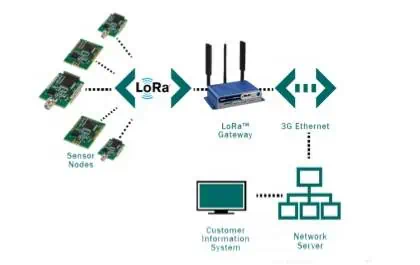
Typical Architecture of LoRaWAN

FULL PCB MANUFACTURING Quote

The typical architecture of LoRaWAN comprises major elements such as End nodes, Gateways, Network server, and Application server.

 End Node

Measurement and control are the primary functions of end node. Also, the end node comprises a sequence of measurement sensors and control elements .
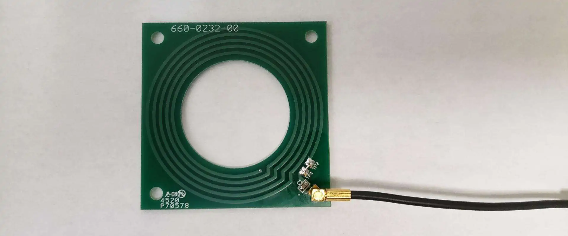
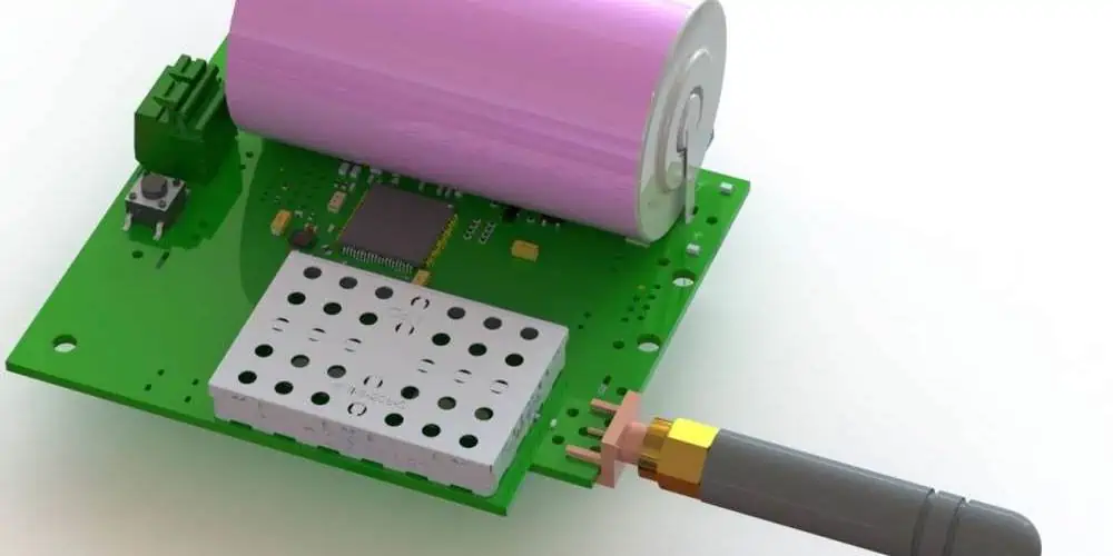
Gateway LoRa

This element receives data from end devices through a radio channel and then transfers the data to a transit network. Also, a star network topology is created by the gateway and its end devices. The gateway LoRa is simply a design that comprises several channels that receives and sends devices that enable the processing of signals that arrive on several signals or channels.

 Ethernet, WiFi, and other telecommunication channels are examples of such networks.

Network Server

This is a centre that initiates network management. The network server helps in setting a schedule. helps Also, it helps in controlling speeds, making analysis, carrying out processing and storage of received data.

Application Server

This is a device used in data collection from end nodes and remote monitoring of their work.

Use Cases of LoRaWAN

There are several use cases of LoRaWAN and some of them include:
Agriculture

LoRaWAN plays a significant role in agriculture. Due to its long range, it offers reliability in rural applications. It is ideal for devices that have low data transmission rates.

 Industrial

Through the digitization of equipment and legacy processes, industrial IoT is simply operations. Therefore, LoRaWAN helps in driving profits, maximizing efficiencies, and lowering  costs. Also, LoRa-enabled devices usually consume real-time data to offer key information into efficiency, machine health, predictive maintenance, and reduced downtime, among others.

 Assets and logistics

LoRaWan is a great option for assets and logistics. This is because it features network-based location and tracking capabilities. Also, this goes for a low cost.

Smart home

One of the most visible applications of LoRaWAN is its use in smart homes. This RF technology can pass through obstruction like walls. Also, it can support battery powered applications ideal for use in smart homes. Therefore, this makes this connectivity a more appealing option.

 Smart metering

LoRaWAN  can get to sensors monitoring utilities buried underground. Therefore, this  makes this an ideal form of connectivity for smart metering. In smart metering, a high level of connectivity is crucial.

Healthcare

 The low power and reliable performance make LoRaWAN an ideal option for connected health applications. Also, IoT solutions which feature LoRa-based hardware help in keeping track of the progress of high-risk patients every time. Therefore, this ensures there is good management of health and medical system.

Where is LoRaWAN Applicable in the IoT Connectivity Space?

Several telecom providers use LoRa . It is like a 3G networks that is specifically built for communications between several IoT devices. Also, LoRa has some data collection systems, in which data transfers need to occur now and then.

Sigfox is another provider of LPWAN systems. This is an ultra-narrowband-based technology. It has already gained popularity in the US.  Furthermore, cellular options like NB-IoT and LTE-MTC or LTE-M are highly ranked and rated in the LPWAN category.

With LoRa and LoRaWAN, the major players seek to provide an offering for companies that want to quickly deploy IoT applications in some areas. In these areas, there are long distances, but there is need for low capacity. For example, in a smart city.

Due to the low frequency and LoRaโ€™s specifications as earlier mentioned,  it is a great option for connected devices that have small batteries. Also, its low power made it ideal for battery-powered connected devices.

The LoRaWAN protocol offers a complete two way communication that ensures security and reliability of the whole system. Also, this protocol is widely used in national networks of telecommunication operators. Therefore, LoRa Alliance ensures the standardization of the LoRaWAN protocol.  Also, the LoRaWAN architecture helps in discovering mobile assets.

What Does The LoRa Alliance Offer?

The LoRa Alliance is an open membership organization whose founding companies comprise telecom operators and technology suppliers. Technology suppliers such as Cisco, MultiTech, IBM, MultiTech, and Microchip among others contributed to the foundation of LoRa Alliance.

Over time, LoRa Alliance is one of the biggest alliances in the technology sector and it has continued to grow. This organization focuses on standardizing low power wide area networks and the improvement of the LoRaWAN. Achieving great application of IoT via the global integration of LoRaWAN technology is the mission of LoRa Alliance. Also, LoRa Alliance aims at empowering sustainable Internet of Things to optimize efficiency, enhance quality of life and as well safeguard the resources of the planet.

LoRa Alliance consists of over 500 members. This goal of this non-profit association involves connecting half of the predicted IoT volumes. Presently, LoRa Alliance has 163 network operators.

LoRa and LoRaWAN- A part of LPWAN ecosystem

There are several Internet of Things (IoT) projects which integrate LoRaWAN  and LoRa. Other networks had been already tested and integrated before the verification of the three cellular LPWA standards. Some companies and even the big ones, have been deploying more IoT applications with LoRaWAN, LoRa,  and the likes.

We need to understand that only a few years ago did the LPWA market begin to gain more attention from big companies and analysts. There are several reasons behind this, but we will be mentioning a few.

The integration of LPWAN is beginning to grow at a fast pace if cellular LPWA is carefully added, even in industrial IoT connectivity

Over time, there has been a lot of controversies as regards LPWAN.  Now, there is now more controversy, on the cellular level. Although, some cellular standards are not commonly used at scale and the journey to 5G IoT is a long way ahead in spite of all the controversies.

 Operators are already deciding on what to do as a 2G network sunset begins to come up gradually, yet only since early 2017. This is definitely far from everywhere in a longer future. There is a higher chance that several countries will switch off 3G networks first.

 Also, the LPWA market is really growing fast even if itโ€™s only a limited aspect of the IoT connectivity market. A good number of operators decided to go for a combination of non-cellular and cellular. For example, LoRAWAN and LTE-M are a great combination for Orange. Also, Orange is not the only operator to go for such combination.

 According to LoRa Alliance, LoRa and cellular LPWA are complements and more operators provide both LoRaWAN and LTE-M.

Why LoRaWAN has Become the Suitable LPWA Standard

There are some differences between LoRaWAN and other LPWA technologies. LPWA technologies offer more set of applications. Also, LPWA technologies allow you to address several applications from a bi-directional connectivity and adaptive rate of data rate. However, the ecosystem is the main differentiator is the ecosystem. If you take a look at the successful integration of technology for the past one decade, you will realize all have followed this model.

The only method to specify volume and deployments is by having several business models, competition, and a vast ecosystem. Another way to receive wide deployment and acceptance is through open standard. However, the various network components such as cloud network,  gateways, chips, and end devices, from various suppliers provides a low risk for  possible end users or operators.

Furthermore, LoRaWAN safeguards data and privacy more than other LPWA. Therefore, it is usually considered the most secure and efficient solution in the market. Furthermore, it has 128AES encryption on various levels for all data. LoRAWAN have become the most popular non-cellular LPWA solutions and ecosystems. Since cellular LPWA options like LTE-M were not available for the types of IoT projects and the applications for LPWAN and cellular standards were very costly and unsuitable for those specific IoT applications, the LoRa Alliance are more efficient than the latest cellular standards.

LoRaWAN connects the LoRa signal to the application(s). Therefore, one can simply say, LoRa is the radio signal that transmits the data. LoRaWAN is the protocol which regulates and specifies how to communicate data across the network

Types of IoT applications LoRa(WAN) Enables

LoRaWAN is ideal for use in several IoT applications. These applications include smart parking, smart metering, traffic, and smart waste management. Also, it is ideal for use in applications that monitor connected devices from a longer distance.

Smart Cities

LoRaโ€™s low power, efficient security, GPS-free geolocation, and long range features make it enhance the efficiency of municipal operations. By simply connecting city services like waste removal, parking, and  lighting, cities can find it easy to maximize the use of utilities and personnel. In the long run, this helps to save time and money.

Smart Gas metering

Meters need to function for longer hours and as well transfer data frequently in a gas utility application. The integration of smart metering technology for gas leak detectors, smart valves, and gas pressure on a similar network is indeed a clear response for gas utilities to improve safety and enhance efficiency.  LoRa devices and the LoRaWAN protocol provide efficient solutions for gas utilities.

Smart Healthcare

Due to the reliable performance , long range, and low cost, LoRa is a suitable option for crucial smart healthcare applications. Also, there are IoT solutions which comprise LoRa sensors and gateways. These  help in monitoring high-risk patients 24/7.Therefore, this ensures there is health safety in the medical industry.

Smart Industrial Control

Some industrial operations benefit from the integration of IoT-connected sensors. This helps in achieving various always-on monitoring functions. LoRa-based devices feature long range, low power, reliable performance, and long battery life. Therefore, sensors in mobile industries or manufacturing plants can supply crucial data to a LoRaWAN where such data can be easily analyzed. Also, this helps in optimizing businesses operations.

What is LoRa Real Range?

Various articles have discussed LoRa distance. Most times, the authors of these articles describe the setting of new world records. Presently, the distance of LoRa is as high as 832 km! However, the question is how are these distances applicable in real-world applications? Does this imply there are hundreds of kilometers in the actual working ranges of LoRa technology? Well, we will discuss provide more answers in these section.

Theory of wireless communication

To have a better understanding on the real range of LoRa, one must understand the functions of range in wireless transmission. Therefore, we must understand the three primary properties of radio networks.  These properties include:

Range

Data transmission rate

 Energy consumption

Each technology requires a balance between these properties. For instance, Bluetooth and WiFi help in achieving high rates of transmission rates at the expense of short range and high energy consumption). However, LoRa technology is different as it involves a low rate of data transmission, which enables transmission over long distances with very low rate of energy consumption.

Conclusion

LoRa and LoRAWAN have become the most popular non-cellular LPWA solutions and ecosystems. Since cellular LPWA options like LTE-M were not available for the types of IoT projects and the applications for LPWAN and cellular standards were very costly and unsuitable for those specific IoT applications, the LoRa Alliance are more efficient than the latest cellular standards.

Most Common IoT Applications and How They Impact Our World

IoT Devices

Internet of Things, commonly known as IoT, has gained popularity over the past few years, and it seems there will be more innovation and development about it in the years to come. However, just like every trending phrases like this, a good number of people are curious about what the IoT entails. Therefore, they ask, โ€œWhat is this, and what are its uses in our world today?โ€

Thatโ€™s why this article is right here. This article seeks to give answers to the above questions. Here, we will be discussing the Internet of Things, different IoT applications, its impacts in different industries and how they are applying it, the trends and future of IoT.

What Is the Internet of Things?

We will start with the basics. There are several definitions of IoT out there. Most time, the definition is usually based on the perspective of author. Here, we will be giving you a straightforward and simple definition. IoT is simply a network of devices and appliances that are connected via the internet. These devices can collect and transmit data without human interaction.

Simply say, the Internet of Things describes the connection of devices to each other and to humans via the internet. IoT can offer relevant data about its operation and that of an activity. These days, several companies from various sectors are integrating this technology.

IoT devices get data and send through some central data server. The data is then processed, distilled, and utilize in making certain tasks easier to perform. When these devices are internet-connected, they  obtain and share data and then make decisions via  Neural Networks and Machine Learning (complex mechanisms).

Devices which are IoT-equipped are refrigerators, laptops, Applewatches, smartphones, coffee machines, Google Home, Fitbits, and many more. Any device that has internet connection and sensors  can be plugged into the IoT.  There are several devices connected across the globe right now. These devices are busy gathering billions of petabytes of data every day.

Most times, IoT is seen as Big Data, since IoT collects the same kind of massive quantities of data characteristic of Big Data. Therefore, all the data from the Internet of Things is Big Data. However, not all information of Big Data is from the IoT.

The government, private organizations and individuals all enjoy the benefits of IoT.

What are IoT Applications?

IoT serve several functions in different aspects of life. These technologies have been adopted in a wide range of industries. You will find then in both government and privately-owned sectors. IoT has helped people to track lost pets, keep track on the security systems of a house, or apply maintenance schedule.

Consumers can make use of the Internet of Things to make reservations for restaurant, keep track of their exercise progress, and a lot more. Also, they can also use IoT to get coupons for a store. Furthermore, businesses can integrate IoT to monitor supply chains, keep track of the spending habits of customers. Also, businesses can keep track and maintain inventory levels, and adopt predictive maintenance of their devices.

IoT has also proved to be very helpful in ITIL, since information technology (IT) departments are required to carry out more functions in a world thatโ€™s becoming increasingly digital. Furthermore, blockchain, which is a beneficiary of IoT is being integrated as a more secure and better method of data processing and transaction.

 All industries need to integrate the Internet of Things (IoT) for solutions looking at the global issues going on. For instance, โ€˜The Climate Pledgeโ€™ reveals its goal of no net carbon emissions by the year 2040. Increasing extreme weather events like floods and wildfires have contributed to this initiative. To make this a reality in the nearest future, companies are now investing in IoT-based energy.

On a larger scale, governments now see the need to minimize the consumption of fossil fuel. This has resulted in automotive companies like Ford to work  on expanding their electric fleets. An increase in the production of electric vehicles will as well trigger investments on smart city planning and smart grids.

Top 10 IoT Applications

Healthcare

The invention and development of wearable IoT devices helps the healthcare industry to keep track of the health of their patients at home. Therefore, this minimizes hospital stays and visits. These wearable devices offer up to the minute real-time information that is life saving. These days, smart beds in hospitals keep patients informed about the availability, and as such reduces wait time for free bed space. The integration of IoT sensors on health-critical equipment indicates more reliability and fewer breakdowns.

Furthermore, IoT makes elderly care more comfortable. The home monitoring sensors can help to know if a patient is suffering a heart attack. The COVID 19 pandemic has increased the integration of IoT technologies in the healthcare sector. IoT offers a better connection between patients, healthcare providers, and pharmaceuticals.

IoT helps in improving the production process at the pharmaceutical. This helps to reduce the prices of drug. Also, IoT helps pharmaceuticals with intelligent inventory management. During the COVID pandemic, IoT technology played a significant role in several capacities. Some of the integration of IoT were vaccine chain monitoring and telemedicine.

Smart Cities

A smart city integrates cellular technology and sensors which are placed in strategic locations like antennae and lamp posts. IoTs have made some cities more efficient. These cities have more energy efficiency and need fewer resources. With the placement of sensors in different strategic places throughout the city various tasks can be carried out.

These tasks include traffic management, pollution monitoring, waste management, streetlights optimization, disaster management, energy expenditure monitoring, smart buildings creation, and more. It costs a lot to maintain public infrastructure like roads, gas supply lines, and street lights.  Oslo, Zurich, Geneva, and Singapore, are examples of cities integrating Internet of Things.

Spain announced its plans to transform the Balearic islands into an Internet of Things laboratory. The country deployed masts to keep record of the levels of noise and air pollution. Also, officials have revealed the need to integrate IoT for managing crowd and improving tourism. Traffic monitoring is another IoT applications.

A smart parking system is being integrated across parking locations in Palo Alto, California. This directs drivers to a parking spot. Also, this system has helped in minimizing traffic congestion. Many cities are transforming into smart cities due to the implementation of IoT.

Smart homes

FULL PCB MANUFACTURING Quote

A smart home is one of the most visible and practical IoT applications.  In a smart home, sensors control security systems, lighting, and resource management. Also, a smart home is usually a smaller version of a smart city. For instance, the Mark Zuckerbergโ€™s Jarvis is an IoT-based smart home system. Also, the smart home system of Zuckerberg integrates natural language processing. The system maintains and regulates lighting rooms according to occupancy. Also, it plays personalized music based on the person occupying the room.

The security system of the Mark Zuckerbergโ€™s Jarvis utilizes facial recognition to inform the family of the their visitorsโ€™ identity. Smart homes have helped in improving home security. Internet of Things allows connection of home appliances like lighting, locks, theft alarm systems, air conditioner, and thermostats, allowing you to control them with a smartphone.

Manufacturing

The manufacturing and industrial automation industries are beneficiaries of IoT. With the development of RFID and GPS technology, a manufacturer can keep track of a product from the beginning of the production process to delivery. IoT can take care of the entire supply chain from the beginning to the end. Internet of Things can gather data on product conditions, environmental conditions, and travel time.

Sensors on factory equipment can help in detecting bottlenecks in the manufacturing line. Therefore, this helps in minimizing lost time and waste. Also, other sensors installed on these machines can keep track of the machineโ€™s performance, thereby predicting when the unit needs maintenance. In the long run, this helps to prevent costly breakdowns.

Industrial IoT is simply the Internet of Things at the industry level. IIoT is the fourth wave of the industrial revolution or Industry. Most industries usually subscribe to computerized maintenance management systems (CMMS). The combination of these systems with IoT-enabled sensors increases the life span of machines and as well ensures reliability and availability.

Agriculture

With IoT, the monitoring and management of micro-climate conditions is possible. This helps to increase production in indoor planting. Devices integrating the IoT technology can detect nutrients and moisture in the soil in outdoor planting. Also, it offers more efficient control smart irrigation and fertilizer systems. The sprinkler systems will reduce wastage if it only dispenses water when needed.

One of IoT application in agriculture is smart irrigation. It helps to use water efficiently for farming. Also, the IoT system will start the water flow when the soil gets to a specific level of dryness. ย Also, it stops the supply immediately it has gotten to a particular moisture level. This in turn minimizes wastage.

Livestock tracking is another IoT application in agriculture. This involves integrating RFID chips to record the location, vitals, and vaccination details of an animal. A smart greenhouse integrates microclimate to increase crop yields rather than depending on changing weather patterns. Also, sensors regulate all important parameters and feature automated systems for water and light.

With Internet of Things, farmers can get valuable information about important things on their farms. Information like acidity level, temperature, and soil moisture can be provided.

Transportation

IoT plays a significant role in the transportation sector.  A good number of people have got to know about the development of self-driving cars and their roles in the transportation system. However, they are just part of the vast potential of IoT in the transportation world. The GPS is a good example of IoT. It helps transportation companies to plot more efficient routes. Therefore, this helps in improving delivery times.

A significant progress has been made in navigation. Also, mounting sensors in fleet vehicles creates an interconnectivity between vehicles and their drivers.  The drivers and owner of the vehicle can determine the operation and status of the vehicle as well as its needs.

Fleet management is an application of IoT that helps with geolocation. ย With this, it is easy to monitor routes and identify the most efficient routes. Also, it helps in fuel savings and performance analysis. This minimizes pollutions in the environment and as well offers vital information to enhance the driving of vehicles.

Smart grids

iot arduino

Utility companies are now integrating internet of things to provide energy. Also, they are now installing appropriate sensors in transmission lines, energy meters, distribution points, and transmission lines. This is what is referred as a smart grid.

Users can now the consumption of energy usage and ensure positive changes in their carbon footprints. Also, it helps in reducing costs. Smart grid allows the creation of energy at solar and wind power plants. Furthermore, smart grid ensures effortless switching between different power sources. They help to maintain correct parameters like voltage while doing this.

Data collected by the Internet of Things can help manage municipal power grids much better as they analyze parameters like usage. Also, these sensors can identify outages faster, and as such, decreases blackout times and improves the response time of repair crews.

A smart grid integrates information Technology to minimize electricity waste, and as such, improves the reliability, efficiency, and economics of electricity.

Water supply systems

When IoT is externally integrated into water meters, this helps to effortlessly collect data, process and analyze data. Therefore, this helps to have a better understanding of consumer patterns. Also, end users  can keep track of their consumption details through an app or web page. The automatic alert is another IoT application in the water supply systems that detect consumption beyond the average range record. Therefore, it indicates the presence of a leak, which has helped to prevent water wastage.

Water recycling is very important. It has helped in water management. Also, the integration of Internet of Things makes water systems more efficient.  This is evident in the consumption of water in a certain area and the amount of wastewater produced.  Internet of Things also helps in waste management.

Wearables

In todayโ€™s world, wearables serve different functions. The production of wearable devices and its use increased in the last three years. From GPS tracking to medical to fitness, wearables play crucial roles in our daily lives. For instance, the fitness bands keep track of heartbeats per minute, calorie expenditure, blood oxygen level, meters of distance covered, and more. These IoT devices look similar to wristbands/watches. Sometimes, they could appear as clip-on devices, earbuds, or smart fabric.

Other examples of wearables are GPS tracking belts and virtual glasses. These energy-efficient devices have sensors and software installed on them. The software gathers and organizes information about users. Brands such as Apple, Fitbit, Samsung, and Google contributed to the introduction of the Internet of Things. Data analytics

Wearable technology is another practical application of Internet of Things. The performances of smartwatches vary. While some read text messages and pop out notifications to keep track of locations, some forecast the weather and provide details about the heartbeat rate. Also, these wearables help parents track their children. Wearables are crucial in elderly care. Constant tracking and location monitoring give well-detailed information about the welfare of the elderly.

Hospitality

IoT has helped in reshaping hospitality in recent years. The hospitality industry has improved with IoT applications. The automation of different interactions like electronic keys sent to each the mobile devices of guest has solved a lot of problem. The application of IoT in the hospitality industry offers easy check-out processes, quicker completion of housekeeping tasks, and sending immediate information on available rooms.

The Internet of Things for automation has helped in reducing costs. Also, you can reduce interactions based on social distancing norms. During the COVID pandemic, IoT helped staff in hotels to reduce the interaction between clients. For example, IoT helped to get rid of the need to personally check into a hotel through the introduction of mobile electronic keys.

Electronic keys inform the hotel management about the location of the guest within the hotel. Also, you can make housekeeping requests and room service via a mobile phone. Artificial intelligence help these devices in collecting data.

What are IoT Devices?

iot-home-devices

When we talk about Internet of Things, we mean connectivity. IoT devices are a type of hardware that can transfer data throughout networks and over the internet. Also, IoT devices are available in a wide range of designs, shapes, and sizes. Also, they perform several functions. Sensors, computational machines, actuators, and appliances are all IoT-based.

IoT devices are usually portable. They are small digital machines that can be taken almost anywhere. Irrespective of their compactness, they perform great functions. Also, these devices help to collect data and analyze data gathered with the help of Artificial intelligence.

Home security devices such as Ring Cameras and even smartwatches are examples of IoT devices. Smart home devices such as Google Nest and Amazon Alexa are IoT-based. I oT devices are specially designed to carry out a wide array of functions. They are ideal for use in a wide range of applications. Also, they enable people to live their daily lives with convenience.  With the help of wearable medical devices and implants, healthcare practitioners can prevent issues and disruptions. Also, IoT devices help to eliminate bottlenecks for business operations.

An IoT device operates like a mini-computer that transmits information to the cloud. After the information has been transmitted, the cloud processes the information. Also, the cloud makes decision concerning the information. For instance, the cloud software can show a notification based on the IoT data transfer.

The majority of IoT devices are primarily designed to automatically function with data. They donโ€™t need any human effort asides  from programming. But, these devices feature a user interface with various functionalities. For instance, some tasks may need you to give permission to carry out actions, while some may carry out the tasks automatically.

Components of Integrated IoT System

The components of IoT system enable IoT devices to carry out tasks based on their programming. Also, these components play a crucial role in the performance of IoT devices. They include sensors, connectivity, data processing, and user interface.

Sensors

The sensors in IoT gather data from the environment. This can be tracking particular operations or gauging temperature.  IoT devices collect this kind of data from their environments. For instance, GPS, accelerometers, and cameras, are means IoT devices gather data to analyze. A motion sensor detects the patterns of vibration in heavy-duty machines and a biological sensor can keep track of various biological functions like acidity.

Connectivity

The IoT device sends the data it gathered to the cloud to process it. Connectivity involves how the collected data reaches the cloud. Also, there are several means of linking IoT devices to the cloud like cellular, WiFi, 5G, Bluetooth, and satellite.

Data processing

It is now time to process the data in the cloud. Computers canโ€™t provide qualitative information yet and therefore, they depend on parameters to read, analyze, and make decisions on inputs. Data processing involves the conversion of raw data into a machine-readable form in such a way that the device understands the next line of action.

User interface

The majority of  IoT devices have user interface (UI). User interface allows people to interact with the IoT device. Also, the user interface produces and offers output to the user. Furthermore, there are several ways an IoT device can function.

Conclusion

The Internet of Things is no longer a new thing. It has slowly gained wide popularity and it is quietly impacting and shaping our future. This technology is simply the outcome of humankindโ€™s curiosity. Also, the intention to live a connected and convenient lifestyle has birthed IoT.  IoT technology simply minimizes labour and gets rid of the chances of making mistakes. There are several applications of IoT. In reality, internet of Things has made everything easier for individuals, companies, and the government as a whole.

Top 10 Electronic Contract Assembly Companies

through-hole assembly process

Electronic Contract Manufacturing, abbreviated as ECM, is a typical technology many companies use for production. The companies are gaining the benefits of growing their scope of services to a large extent. We will elaborate on the different aspects of the ECM in detail for your easy understanding. Let’s start discussing it without further ado!

What are Electronic Manufacturing Services?

Electronic contract manufacturing is a complete package of solutions. There are different sub-services like component supply, designing, and production of prototypes. The services also include the PCB assembly and testing of the printed circuits as well. There are different companies that offer variable partnerships in their businesses. The clients leave their orders with delivery time and their requirements.

The production companies would leverage all their professional skills for the production of the printed circuits and other counterparts. These products have vast applications in different global domains and commercial sectors. These products serve as the backbone for these domains. The associates of these companies are professional and adept. This leads to short production time for the clients as well. 

Services of Electronic Contract Manufacturer

pcba box build assembly

ยท        ECM is a huge umbrella of services that includes almost all the possible services related to printed circuits. The technology of electronic contract manufacturing is a crucial factor in the sustenance and progress of the electronics sector. 

ยท        Some clients need the services of the R&D department as well. This department would provide the design services and would produce the hardware that is needed for the electronics. The companies would collaborate with other firms and will ease the process of printed circuit board assembly for the users. 

ยท        Some clients know the process of design on their own. They will discuss it with the firms they are hiring. These firms would help these clients with the production and assembly of the printed circuit boards. 

ยท        The element of outsourcing is essential since ECMs would seek help from others for the procurement of important counterparts for the electronics. Outsourcing proves to be reliable since it will remove the odds of any complications. 

History of Electronics Manufacturing and Contract Assembly

This sector came into existence many years before. Those were the days when Selectron started to impress the world. The in-house PCB assembly was the sole trend at that time. Since the giant producers would rely on this method.

When electronic contract managing services started to develop, these turned the tables for many people. These were easier to execute. Offered greater feasibility as well. It hugely excluded the labor costs and pertinent issues. After this, the surface mount tech was also considerable. This was important for the fast-paced production of printed circuits. 

Benefits of Electronic Contract Assembly

1.     Excellent Quality standards

The ECM firms are more reliable in terms of the quality that comes with their products. These are experienced people and know the subtle art of addressing the client’s problems. They can deal with a variety of electronics, meeting the expectations of several clients. These firms are well-aware of the different dimensions of this sector. Take care of small details for the people. They never compromise the quality of their produced goods as well. 

2.     Lower Costs

The domain is beneficial in terms of lower production costs and investment amounts. Since technology is progressing at a rapid rate, it’s becoming more expensive at the same time. Also, the trends are always fluctuating, so the prices would be variable in different intervals as well. Consumer needs and demands are also differentiating factors.

The ECMs are important to consider for affordability. You can get your hands on quality products with a reasonable amount of investment. The firms cannot only save you a lot of investment. But also will do the revisions if you ask them. 

3.     Fast Turnaround Time and rapid assembly

The turnaround time matters a lot. ECMs are reliable in this aspect. This is due to the fast production and delivery mechanism offered by such companies. These focus on fast production. So that the goods can be transferred to the market. The companies start getting revenue as soon as they transfer their productions to the electronics market. These companies expedite the process. Without any second, these leverage all of their power to render you what you need. 

4.     Specialized Manufacturing Services

The domains like defense, aerospace, and automotive need high-end products that are flawless in their performance. These go through hefty quality control methods and get shortlisted for the market supply.

In this case, you need to consider an appropriate ECM company to avoid all the possible complications. Make sure to check their portfolio, client reviews, and style of working. The certified and experienced companies would be your lifesaver in urgent need of production. 

Applications of Electronic Contract Assembly

FULL PCB MANUFACTURING Quote

The importance of ECM services cannot be ignored. There are different domains that would barely survive without this service. The benefits of ECM include bulk production without human and technical errors.

Also, high-quality products are high-tech for consumers. So that they can use and rely on these products in daily usage, these are affordable as well so that everyone has equal access to these products in the market. 

Top Electronic Contract Manufacturers and Assembly Companies

1.    Foxconn 

Foxconn is a leading ECM company. The company operates from china. The services of the company have been benefiting users for the past several years. The company has international ties as well. The company has different special services for users. The domain of consumer electronics has made great contributions to the company. The services include the production of electronics like computers. It also deals with the business of electronics components. 

2.    BYD Electronics

BYD Electronics is another Chinese ECM firm that started its business some years ago. The company itself is among the top producers in this domain. The brilliant products of the company include laptops and smartphones. Smart systems of automotive and other electronics products. The company was formerly a producer of batteries, but these days the company is now exceptional in its multiple services and products. 

3.    Pegatron Corporation Technology Company 

Pegatron is a famous firm in this aspect. It’s a globally active company for the services that fall under ECM. The company is functional in China. It offers flawless product development and production of electronics that can be used in various domains. The company also offers you services of computer designing and production of multiple electronics. 

4.    Flextronics China

Flextronics is a Singaporean producer of electronics. It’s another considerable ECM firm that you must shortlist for consultation. The company has offices in different regions of the world. By this, you can have an idea of the magnitude that the company works on. It’s among the biggest ECM firms around the globe. The company produces exceptional designs and products for consumers. These products would be reliably used in different domains for quick and safe benefits. 

5.    Jabil

Jabil is an American ECM firm. The company came into existence many years back. The solutions offered by the company are still in use. The designs and prototypes are useful. The company has several contributions and collaborations with other companies for the sake of the development and progress of the electronics sector. The company serves you for products used in data transmission and automation. The company also operates in China. 

6.    Luxshare Precision Industry Co., Ltd 

Luxshare Precision is another Chinese ECM company. The services of the company include designing and production of the cable assembly. Also serves you for the connector system. The connector system would be beneficial for the domains like automotive and consumer applications. It is a production associate for several renowned smartphone brands as well. 

7.    USI Global 

USI operates from China. The company focuses on the design and production of electronics. The company also specializes in the process of miniaturization. It procures the production materials. Takes care of logistics. Offers communication and maintenance services as well. 

8.    Wistron

Wistron is the largest producer of laptops and operates in China. The company has giants of the electronics sector as its clients. The additional services are electronics products like wireless chargers, antennae, modules, and motors. All these are typical products that are of use by thousands of global consumers. 

9.    SANMINA China

Sanmina operates from America. The company has a huge portfolio of exceptional products and services. The products from the company are used by several people. The company generates a decent amount of revenue from the services it offers. The services include automotive products, products for design and development, and many others. The semiconductors production of the company is reliable for different domains like automobiles and defense systems.

10.                    Inventec

You must consider this one for the remarkable ECM services. It’s an incredible notebook computer producer. The company researches and develops its products with complete care. The computers of the company would be used in different sectors around us. The computers are of high quality and also serve you longer. The company emphasizes green energy, which is an exceptional feature of the firm.

Conclusion

ECM is a brilliant way to leverage a company’s skills for your own good. So that you can acquire the desired products with much ease, these products would also serve you longer. The discussion was to render you all the knowledge about this system on a deeper level. 

Features, Functions, and Benefits of 2.4 GHz Patch Antenna

Rectangular Patch Antennas

This article discusses a miniaturized 2.4 GHz patch antenna for wireless connections. First of all, a conventional microstrip-fed patch antenna operates close to 10 GHz. This antenna is redesigned to operate at lower frequency. Also, a uniplanar-compact-photonic-band-gap replaces the ground plane.

What is 2.4 GHz Patch Antenna?

Patch antenna are usually integrated in indoor settings. You can connect the 2.4GHz patch antenna for wireless access points. Also, this patch antenna is suitable for linking two locations without the need for wires. The 2.4 GHz can share data or integrate a VoIP wireless link. You can link the 2.4GHz directional antenna to Netgear, Cisco, ZyXel, Linksys, D-Link or other WAP (Wireless Access Points). This helps in achieving more signal strength.

The wireless signal will transmit more if the access pointโ€™s transmit power is stronger. Therefore, this offers a better enjoyable Internet experience for people. The Transmit Power on Belkin, Linksys, and Dlink Wireless Access Points (WAP)  is usually within the range of  15dbm, or 32mW Transmit Power.

Therefore, this only indicates that when you link a high gain antenna, it will provide a helpful solution to your range. However,  it wonโ€™t offer a better distance and signal strength a 200mW Access Point will offer. With an outdoor patch antenna, you can easily get the best range. You will need to upgrade your D-Link Access point. Rp sma

2.4 GHz Patch Antenna is a commonly used antenna and has been widely used across a wide range of sectors because of the benefits it offers. This antenna is a low profile, lightweight, and low cost option. It has got good mechanical strength, high gain, wide frequency band.

Due to their low cost, simple design, and small size, these patch antennas are easy to use and install. 2.4 GHz Patch Antenna is ideal for use in wireless communications like mobile communication, radar, navigation systems, and satellite communication.

What are the Features of 2.4GHz 14dBi Outdoor Directional Antenna GNS-1403?

The 14dBi directional antenna offers a lot of features. These features make it an ideal option for connection two locations without the need for wires. Below are some of this antenna features:

  • It has a coverage area which offers extended point to point linking
  • This outdoor directional antenna comes with weatherproof enclosure which helps in outdoor deployment.
  • It has an N-Type Female connector. This works perfectly with most of access points / wireless routers.
  • Also, it offers easy installation mounting kit such as L-Bracket and U-Bolt.

What is the Function of this Antenna?

The Outdoor Directional Antenna GNS-1403 is an effective antenna that functions in the 2.4GHz band. Also, it offers 14dBi directional operation. Therefore, this extends to the wireless range and offers improved Wi-Fi performance.

Also, the 2.4GHz directional antenna comes with N-Female connector. The N-female connector is an important feature which helps in linking to any outdoor or indoor access point with the use of a coaxial cable.  Ground plane Furthermore, it is very compatible with the majority of wireless access point.

The Outdoor Directional Antenna GNS-1403 offers wireless connectivity at more distances. Therefore, it allows you to enjoy the advantages of wireless connectivity at much greater distances.  Another benefit of this Outdoor Directional Antenna GNS-1403 is that it requires no installation or configuration software.

Benefits of 2.4GHz 14dBi Outdoor Directional Antenna

Easy To Use

It is very easy and straightforward to install the 14dBi patch antenna. If you are using this antenna for the first time, you will find it so easy to install. Also, this antenna works well with most wireless device such as Routers, Network Adapters, Access Points and Bridges.

Range and Performance

Decibels (dBi) represent the measures the power rating of Wi-Fi antennas. The majority of standard rubber duck antennas measure more than 2 dBi. However, the GNS Wireless 14dBi patch antenna enhances power to 14dBi.

Also, Your wireless signal is concentrated to an outdoor directional antenna directly towards your networkโ€™s wireless source. Therefore, this leads to a huge increase in wireless distance. You can pair the outdoor directional antenna with another Hi-Gain 14dBi antenna to create a point-to-point solution. This solution will be much farther than the normal coverage.  

Plug and Play Installation

Installing the GNS Wireless outdoor antenna is a very simple process. This is because it works well with most wireless devices with removable antennas in the market. Also, the 14dBi antenna comes with a great feature which is N-Type connector. This helps in supporting various wireless devices.  It is crucial to know that a  low loss antenna cable will be of great need for outdoor installation. Also, you should purchase the antenna cable separately.

You need a shorter cable to achieve less signal degradation or cable loss because of the cable length. However, this depends on your set up. The 13dBI 2.4GHz with N-Female connector can be connected to any indoor access point that has removable antenna such as ZyXel , Linksys, Netgear, Cisco, D-Link, or other Wireless Access Point for improved signal strength.  

Furthermore, the 2.4GHz directional patch antenna is ideal for linking two locations without wires, data sharing, or integrating a VoIP wireless link. Also, you need coaxial cable types and connectors to operate this 2.4GHz patch antenna. However, it is crucial you ask your supplier some questions. You can search for Videos online to know more.

The wireless signal will carry more power if the transmit power of the access point has more strength. Therefore, this will offer a more enjoyable experience from your customers. You can link the 2.4GHz directional antenna to Netgear, Cisco, ZyXel, Linksys, D-Link or other WAP (Wireless Access Points). This helps in achieving more signal strength. Cart buy

The wireless signal will transmit more if the access pointโ€™s transmit power is stronger. Therefore, this offers a better enjoyable Internet experience for people. The Transmit Power on Belkin, Linksys, and Dlink Wireless Access Points (WAP)  is usually within the range of  15dbm, or 32mW Transmit Power.

Conclusion

Patch antenna are usually integrated in indoor settings. You can connect the 2.4GHz patch antenna for wireless access points. Also, this patch antenna is suitable for linking two locations without the need for wires.

Altium vs Eagle: What is the Difference?

Altium Designer 20

A PCB design automation tool and software were created by the Australian software company Altium. It is currently the most popular and well-known program in the electronic design business. Also, it includes a schematic PCB module and an auto-router. It also includes pairs for differential routing.

Additionally, it facilitates the turning of the track length as well as 3D modeling. It offers a variety of software engines and editors for electronic product development. It aids in managing processing, compiling, and editing. This program also offers X2 integration. Since the environment is completely adjustable, one can arrange the workspace to suit the situation.

What are the Features of the Altium Designer?

The following are a few strong characteristics offered by the Altium Designer:

  • Turning of the track length and 3D modeling
  • Powerful Data Management Tools;
  • real-time transparency and cost estimates
  • Modern technology for routing,
  • Cutting-edge as well as rigid support for flex board designs
  • Flexible tools that help in managing release

Altium Designer supports and provides all of these functionalities inside a single design environment. It is designed to offer the highest productivity possible.

Additionally, Altium Designer’s unified functionality allows for easy transfer of design-related data from one of the design stages to another. The learning curve could be enhanced with the aid of its plethora of features in order to boost productivity.

It specifically aids engineers and scientists in keeping up with all facets of electronic design procedures.

After many attempts from developers, this software now offers a unified and single environment for designing. Because of this, Altium Designer is currently a widely used tool for designing PCBs.

Altium Libraries

Altium PCB

This also includes a collection of libraries that are a haphazard assortment of various functional parts and models. However, how the user arranges the parts or models in a library is entirely up to them. Libraries are typically organized around the device suppliers, for example, a library per each type of micro-controller that a business employs. There are several different Altium library types, including:

  • Schematic library (the simplest library and typically the model library)
  • PCB library (being used in storing footprints of 3D models)
  • Integrated library (composition of PCB and schematic library)
  • Database Library (Useful for the insertion of the design components in the data of the company)

Altium License

There is a streamlined Altium license mechanism that enables the program to be used in the most effective and efficient manner possible. By using this technique, licenses are distributed to the appropriate users. This system offers two different kinds of licenses. Its web-based licensing mechanism is at the top. Customer accounts are integrated into it. Users who have this license can use the software on any PC or computer without having to verify it, and there is also no need for extracting or copying these license files in order to activate the product.

Four different kinds of licenses for Altium are available. These include:

  • On-Demand License (Observes the release and use system. The client’s computer will be able to acquire an on-demand license after logging in.
  • Standalone License (you can obtain this license through the extraction or copying of the license files).
  • Viewer License (This is connected to the Altium account of the user.) Users can access software without a license thanks to it. Also, you cannot access the license through the dashboard.
  • Private Sector License (This is adopted by the Altium Infrastructure server. This offers remote software installation as well as license management.

Benefits and Drawbacks of Altium Designer

The advantages are as follows:

  • It is simple to switch between a 2D or 3D body based on the requirements of the design.
  • It enables the use of STEP models.
  • Mechanical data could be integrated into a specific design to keep track of the 3D models;
  • It can assist in updating previously recorded designs, resulting in increased efficiency and organization in the development and design of PCB.
  • You can resolve issues in 3D models in order to see which mechanical adjustments and other changes suit your system.
  • Data sharing with MCAD systems is simple.
  • Created to satisfy the requirements of any engineer who creates electronic products. Furthermore, it is a more advanced technology offering better value.
  • It offers a great circuit board layout editor with nourished behavior and control.

This software has the following drawbacks:

  • With its default settings, a schematic of medium-size results in numerous specious warnings.
  • Because it is a big piece of software, startup times can be lengthy.
  • Slow file access when using a network, if possible.
  • Altium has many restrictions, making it challenging in routing the designs.
  • The auto-routers ‘restrictions
  • It offers less features than similar programs and software
  • The costliest EDA software, making it unaffordable for SME’s.

Price of Altium designer

The starting pricing for Altium Designer is 295 euros. There are two different license types for this software:

  • Perpetual License: Starts at 2 685 euros and includes a standard subscription for updates.
  • Time-Based License: This is the subscription model, starting at 295 euros.

You can test an Altium product out using the Free Trial edition of Altium Designer. Also, you only need to complete a brief form to create a new registration. You will be sent an email in return with access to the Free Trial.

What is Eagle PCB?

FULL PCB MANUFACTURING Quote

Eagle stands for Easily Applicable Graphical Layout Editor. This program aids in electronic design automation.

It enables electrical designers, in particular those who create printed circuit boards, to seamlessly integrate several PCB’s schematic layouts. Along with PCB layout, library content, It aids designers to determine optimal functionality, and component replacement. Depending on the use, this software is either cheap or completely free.

Premium Features of Eagle

Every engineer can now have reliable designing. By delivering improved printed circuit board layout, various contents from pre-designed libraries, various tools for schematic editing, as well as community-driven features, it enables designers to translate their approaches and vision into reality.

Professionals that desire limitless board space and go beyond the bounds of circuit board design have been specifically targeted by Eagle premium.

The schematic sheets are about 999 in total, with 16 single and plane layer counts.

There are several new features included within the Eagle Premium. These are listed below:

There is a new automatic router being installed. As a consequence, the procedure is complex, and fewer transition boards get created than with algorithms employed in earlier or competing software. Less manual contact is required from the user, and the cost of the boards is ideal.

For Eagle Premium, hierarchical designs were created to handle such large schematic designs into small functional pieces or blocks. These designs will subsequently be distributed to different team members. In the end, an integrated design would arise from the team’s collaborative design work.

Additionally, this design could be repurposed by using designs from one block in another.

A block’s face in an (IDF) file displays the maximum component dimensions, such as height and length. IDF files for circuit boards can now be uploaded into the Eagle Premium. When it comes to compatibility, just mechanical programs work here.

Users can now be entertained by Eagle Premium’s 7th version thanks to its updated interface and graphic design. New, self-explanatory icons and graphics have been added. Users can now choose between a classic or a modernized icon style.

PCB Eagle Library

With Eagle software, pre-installed as well as out-of-the-box libraries are both available. Various pre-designed symbols, components, parts, footprints, and 3D models are covered by the libraries of the Eagle PCB.

Additionally, there are numerous worry-free libraries available online on its website. A board’s design is an extremely time-consuming process that can require 8 to 12 hours of the designers’ effort. Eagle provides libraries that give users access to parts and components that have already been created, saving designers the time and effort of creating a variety of new components. Additionally, the user can use the library to search for and place a part. With Eagle PCB libraries, design engineers may ensure perfect fit of a board in its location without depending on luck.

Eagle License

Regarding licensing, this software’s system was typical with upgrades and few improvements 25 years ago. Eagle has since joined the Autodesk family that boasts a superior development team. Also, a specific method exists for ongoing updates. Users of this system can receive frequent upgrades with lots of improvements.

Eagle’s family is supported round-the-clock by a system. Additionally, the software is now affordable and available to everyone thanks to monthly and yearly packages. Customers can choose between three license types: free, per month, and yearly. Monthly and annual eagle licensing fees vary. Additionally, free license has less restrictions.

The key performance elements of the EAGLE licensing package are listed below in case you don’t know about it. However, if you currently own an Autodesk software, including such Fusion 360, you will be familiar with the subscription version.

  • Ability to choose your preferred subscription model. There is no requirement to pay for software you are not using on a regular monthly as well as annual basis.
  • Automatic updates save a lot of money because they are sent without human intervention.
  • Making jobs with no restrictions. A broad range of capabilities are made possible by the most recent advancements used in this software.

The performance of the most recent Autodesk EAGLE version has improved when it comes to manufacturing models for the PCB layout, editing design schematics, and utilizing many already completed projects. With variation 7.7, the production process has been improved. Updates are released often and regularly.

Limitations of Eagle PCB Free Version

How to Panelize in AlTIum Designer

These are some restrictions on the software’s free version:

  • A small board area.  For the free version, the user is restricted to a specific area. Only the dimensions of 100 x 80 mm can be changed in the PCB design.
  • Only two separate layers may be used in the free version.
  • The inability to use several sheets in the schematic editor is a huge restriction in the free edition.
  • The free edition is also limited to email or team help.
  • For individuals who are interested in learning it or are hobbyists, there is a free version available. Free versions are only permitted for non-commercial uses.

What is the Price of Eagle PCB?

Choose from one of the three Autodesk FUSION 360 membership plans to access the full edition of the EAGLE Premium.

Three alternatives are available:

  • Three years
  • One year
  • One month

Fusion 360 package also includes:

  • Reporting of Product Usage gives you the option to view the product usage data by specific users.
  • Autodesk Drive allows you to share data between projects.
  • Security and administration – two-step verification
  • Shared Views – Workflow views that can be viewed by authorized users;
  • Support service: Online assistance is available 24/7.

Standard, Education, Enterprise, and Premium are the four distinct varieties of Eagle Premium.

Eagle vs. Altium: What’s the Difference?

  • When comparing the two programs, Eagle offers more capabilities for team collaboration or integrated design. In terms of projects that are hardware-based, Eagle offers better alternatives, although Altium’s user interface is more dependable and potent.
  • When it comes to cutting-edge features, Altium provides numerous additional and better ones than Eagle, like digital processing of high speed.
  • Altium’s design rule checking is also far more trustworthy than Eagle’s. Altium has advanced accommodation and routing for the radio frequency.
  • When it comes to cost, Eagle is less expensive than Altium. Eagle offers three different modes. There are far fewer limitations in the free version as well.
  • Another problem with Eagle is how hard the library handling is. Handling libraries and creating custom components is significantly simpler in Altium.
  • Eagle is a far better alternative for simulations over Altium with the inclusion of Fusion 360.
  • One drawback of Altium is that it can only run on Windows, but Eagle Premium can work on any operating system.

Conclusion

Which is preferable, then, depends entirely on your needs and available funds. Therefore, if you have the money, Altium is the right alternative to think about. However, Eagle could be a perfect option if the consumer has financial restrictions.

What Are Different Types Of RFID Antenna And Their Working?

RFID Antenna

A transponder, transceiver, and scanning antenna are the three main parts of every RF identification system. An RFID interrogator or reader is a transceiver and scanning antenna in one convenient device. RFID readers can either be permanently installed or portable.

The Radio-Frequency ID reader is a portable or fixed device that connects to a network and reads tags. It sends messages to the tag via radio waves, which causes the tag to become active. After getting activated, the tag will return a wave that will get picked up by the antenna and decoded.

The RF identification tag itself contains the transponder. RFID tag read ranges change depending on a number of parameters. They include the reader and tag design, RF identification frequency, and environmental and peer interference. More powerful tags are readable from even further away.

How To Select An RFID Antenna?

rfid antenna types

The Radio-frequency ID antenna receives energy from the RF identification reader. And broadcasts it as radio waves to any RFID tags within range. Antennas are the hands and feet of an RFID system. They are responsible for sending and receiving data between RFID tags and readers. Most RFID antennas have a standard, uniform design. Differences emerge from their unique anatomical characteristics. There are many factors to think about when selecting an antenna. They include polarization, opening beamwidth/angle, amplification, and frequency range.

ยท Frequency Range

Each country has its own rules about what sort of UHF/RFID frequencies are legal to use. In general, UHF RF identification antennas operate in one of three frequency bands:

  • EU/ETSI 865โ€“868 Megahertz
  • US/FCC 902โ€“928 Megahertz
  • Other global bands 860โ€“960 Megahertz.

Pick a radio frequency identification antenna with a frequency range appropriate for its intended use area.

ยท Amplification & Opening Angle

In physics, the relationship between opening angle and gain, or beamwidth, is particularly strong. Since a narrower radio wave has a higher gain, it can cover less ground but travel farther in a single beam. In conclusion, the amplitude of a wave affects its overall width. Higher amplification results in a more concentrated wave.

Different intensities of a flashlight beam can be used to illustrate this concept. In this case, the answer will determine which antenna should get chosen. An antenna with moderate amplification power and a larger beam is ideal if there are multiple tags in close vicinity.

ยท Polarization

The polarization of most RFID Ultra high-frequency antennas is either linear or circular. Therefore, antennas with linear polarization only radiate radio frequency energy in a single direction. It can be in either a horizontal or vertically direction. Antennas with a circular polarization radiate wave in a spherical pattern, either counterclockwise or clockwise.

We make a distinction here between LHCP and RHCP. It’s crucial to determine whether or not an array of antennas is RHCP or LHCP if they’re all pointed in the same direction. The overlapping of circular antennas with the same polarization is possible by deploying antennas with counter-rotating circular polarizations. A larger, more productive reading area becomes establishable.

Which RFID Antenna Is The Right One? Circular Polarization Or Linear Polarization: 

A lot of rides on whether or not an RFID system uses a circularly polarized antenna as opposed to a linear polarization antenna.

In the case of EM waves, the linear polarization effect occurs when the waves get transmitted in a single direction (vertical or horizontal). When all RF identification tags are vertically aligned, and at the same height, linearly polarized antennas perform the best. A linear antenna’s concentrated transmission allows it to outperform a circular antenna of equal amplification in terms of reading range.

When the orientation and location of an RFID tag become unpredictable, omnidirectional antennas are the best option. Their waves have been likened to a corkscrew turning in 2 dimensions. Because of the two-dimensional power loss inherent with omnidirectional antennas, their reading range is inferior to that of linear antennas.

Understanding how antennas function and how RF identification tags get oriented with respect to the antenna is crucial when deciding on the type of antennas that will get used in an RF Identification system.

Different Types of RFID antennas

1. Small & large RFID antennas

Antennas range in size from those designed for mobile phones to those designed for television sets. A size disparity is an excellent indicator of possible reading distance. For a given read range, a larger antenna will provide a greater effective distance. The antenna you choose may also get affected by where you decide to install it. Large antennas may not be suitable for certain installation sites due to space constraints or aesthetic preferences.

2. Internal & external RFID antennas

Aspects of the system could be water and dust-resistant because RF Identification can be used in virtually any setting. All electronic components get verified as dust and waterproof to at least one of the standards set out by the American IEC 60529 and the British EN 60529. Working temperature is considered while deciding whether or not to use the antenna outdoors. In order to function at their best, the antennas can only get exposed to certain temperatures. The antenna’s performance degrades or stops altogether when moved outside this range.

3. Integrated & non-integrated RFID antennas

Antennas are purchasable independently of the RFID reader or packaged together in a single device. The elimination of the need for wires allows for a more compact and portable system to get constructed when integrated devices are used. Because such a solution is typically smaller, simpler to operate, and more aesthetically pleasing than two difficult portable drives, it may be the best option for distribution and retail settings. However, external antennas offer a broader range of design and application options.

How Does RFID Antena Work?

FULL PCB MANUFACTURING Quote

In the family of technologies known as AIDC, RFID is one member. Automatic identification and data capture (AIDC) techniques can be used to recognize things automatically, gather information about them, and input that data into computers with minimal human involvement. RFID systems do this by sending a signal across the air using radio waves. There are three main parts to any RFID system: the tag itself, the reader, and the antenna. Data is transmitted from the RFID tag’s IC through its antenna to the reader. The reader is also known as an interrogator. After receiving the radio waves, the reader transforms them into a more usable format. Data from tags get transmitted via the communication menu system to a host machine, where it gets entered into a database and prepared for further analysis.

Challenges

There are two basic problems with RFID:

ยท Reader Collision

When two or more RFID readers are in close proximity to one another, a phenomenon known as reader collision can occur. To avoid this, an anti-collision strategy can be implemented to have RFID tags alternate between broadcasting to different readers.

ยท Tag Collision

When a large number of RFID tags try to send information to a reader at once, this is known as a “tag collision.” This is avoidable by using a reader that collects tag data sequentially.

Layered PCB – How Many Types Of Layers Of PCB Are There?

Shengyi S1190 PCB

The layers of copper on a PCB are laminated onto or between other layers of conducting material and are referred to as PCB layers. Adding more layers allows electronic components to do more complex tasks. This article introduces the idea of layered PCBs. Besides this, it will also describe the many kinds of layers as well as the advantages of each.

What is a Layered PCB?

One or more layers of conductive and dielectric materials get layered together to form circuits. These circuits are then used in the production of a wide variety of electrical gadgets. Also, they have a usage in a variety of industrial equipment. These include the consumer electronics, medical, military, aerospace, telecommunications, and automotive sectors.

PCBs are in use to support and connect electrical parts in electronic gadgets. And are typically fabricated from copper, resin, and a substrate. The capability and strength of a PCB are directly related to its size and number of layers. Adding more layers to a PCB increases its functionality. This has significant advantages in the electronics industry.

Different types of Layered PCBs

Rogers pcb circuit board

1.   Single-layer PCBs

Single-layer printed circuit boards (PCBs) are a form of circuit board that has only one thin coating of conductive material (often copper) on one part of the board. The other part serves as an attachment point for various electronic parts.

Therefore, electrical boundaries, fillers, connectors, components, wires, mounting holes, vias, and pads are all fabricated using a single-layered PCB substrate, conducting metal layer, silk screen, and protective soldering mask.

The electronics industry still relies heavily on single-layered PCBs despite the advent of more advanced technologies.

Pros of Single-SIDED BOARDS

  • Cheap to produce
  • Simpler and less error-prone to develop
  • As there is only one layer. So, soldering, mounting, and electronic drilling components are simple.
  • A good choice for minimalist layouts
  • economical for mass-producing consumer electronics
  • The best choice for fast, mass production.

Drawbacks of a Single-Layer PCB

Single-layer PCBs have the benefit of being simple and inexpensive to produce. But they also come with a few drawbacks that users should be aware of.

  • There is a lack of room and pins for connectivity on printed circuit boards that need several components.
  • Reduced velocity and productivity.
  • As functionality increases, weight and size also increase, making the device less portable.

Coffee makers, calculators, radios, and even some types of cameras and cell phones use single-layered PCBs because of the space and weight savings they provide.

2.   Multilayer PCBs

Stacks of double-sided circuit boards are used to create multilayered PCBs. It is common for these stacks to include three double-sided circuits. But they can include as many as necessary. However, warping or twisting may occur after soldering if the layer numbers used are odd.

Printed circuit boards with several layers get manufactured by laminating core materials and prepreg layers at high temperatures by melting the adhesives that keep the layers together and making sure that the conductors are thoroughly coated by resin. This procedure guarantees that no air gets captured in between layers. Epoxy glass, ceramic, and Teflon are a few of the many possible combinations of material used in multilayer PCB construction.

Multilayer printed circuit boards have a usage in a wide variety of electronic devices. Some examples include laptops, file servers, global positioning systems, heart monitoring systems, medical apparatus, handheld equipment, satellite systems, signal transmission, space probe technology, nuclear detection system, and cat scan system.

Benefits of a Multilayered OR DOUBLE SIDED PCBs

FULL PCB MANUFACTURING Quote

ยท        Appropriate for complex projects

With the addition of more layers, multilayered boards may accommodate more circuits and connections. This allows the board to get used in devices that are more complicated. And, so require more components and circuits.

ยท        Durability

More layers mean a thicker, more robust board. This will allow the board to survive rough treatment and maintain its integrity for longer.

ยท        Connection

When using a single-layer PCB, many components would typically require multiple connection points. With this benefit, manufacturers can create compact and lightweight gadgets with minimal design requirements.

ยท        Increased Capacity

Power-hungry gadgets can benefit from multilayer PCBs because of their increased density. This means more robust devices can function effectively.

Drawbacks of Multilayer Layer PCB

ยท        Costly

To create a multilayer PCB, more resources, knowledge, and time are needed. Thereby, they are significantly more expensive than a standard single-layered board. The manufacturer is responsible for ensuring that the multilayered board will get used in a worthwhile project.

ยท        Longer Lead Times

Multilayered boards take more time to design because of the complex needs of the layering phase.

Due to the complexity of the production process, the time required to complete it gets increased.

ยท        Challenging to Repair

Repairing a malfunctioning PCB with multiple layers could be challenging. This is due to the fact that the problem’s origin may lie hidden within a layer that is not visible from the exterior. As the number of layers on the board increases, so makes it is difficulty to fix it.

Multilayer printed circuit boards are typically characterized as rigid PCBs. Because of the difficulty in fabricating flexible multilayered PCBs. The typical number of layers for a multilayer PCB is between four and eight. Cell Phones can have as many as twelve layers. Though that number largely depends on the complexity of the software in use. Also, companies prefer an even number of layers over odd ones when laminating. An odd-numbered layer might lead to an overly complex and problematic circuit. The high price tag is also something to think about.

However, a typical multilayered PCB consists of the layers listed below in the following stackings:

3.   Two-Layered Printed Circuit Board

Both sides of the double-sided PCB are copper-plated, and an insulating layer lies in between. A double-sided printed circuit board is similar to a single-sided PCB. But features elements on both parts of the board. They are made by sandwiching a dielectric substance between two copper layers. And then connecting the two layers together. Systems where small packaging and high-speed are desirable benefits from the copper on both sides’ ability to convey various electrical signals.

The dielectric material in the middle prevents the electric signals from interfering with each other as they travel between the two copper layers. The most typical and cost-effective PCBs to produce are those with only two layers.

4.   Four-Layered PCB

PCBs with four conducting layers are the four-layer PCBs. These layers include two inner layers, a bottom layer, and the top layer. The bottom and top layers are for elements and signal routing. At the same time, the inner layers comprise the core and are typically utilized as ground or power planes.

Soldering masks with uncovered pads provide mounting locations for through-hole parts and surface-mount gadgets. They are commonly applied to the outer layers. When the four layers get laminated together, they function as a single board, with connections made through holes.

Just to give you a brief idea, these layers are as follows:

The first layer is the base and is often constructed of copper. It’s there to keep everything else on the board fixed.

The power plane is the second layer. Its name comes from the fact that it is responsible for supplying the board’s various parts with a steady and pure supply of energy.

The third layer is the ground plane. It provides a common ground reference for all the circuitries.

The top layer is the fourth layer. It handles signal routing and component interconnections.

This is how a typical four-layer printed circuit board gets stacked. But, it can get changed to accommodate different designs or the layer carrying the most signals.

There is a wide variety of uses for four-layer PCBs since they are so much more flexible than two-layer PCBs. Strong signal quality and temperature control are further benefits of the extra layers. These are only some of the many reasons why they are preferable over two-layer PCBs.

5.   Six-Layered PCB

A six-layer printed circuit board (PCB) consists of a four-layer board with two additional signal layers inserted between the planes. Four routing layers (two external and two internal) and two internal planes make up the basic six-layer PCB pile (one for power and the other for ground) by providing two inside planes for high-speed transmissions and two external layers for routing low-speed data. EMI is greatly amplified. An electronic gadget’s signaling can get disrupted by electromagnetic interference (EMI). It can come from either induction or radiation.

There are a variety of possible configurations for a six-layer PCB stack up, with the amount of ground, signal, and power layers depending on the intended function.

The bottom layer, prepreg, internal power plane, core, internal route layer, prepreg, internal route layer, core, internal ground plane, prepreg, and top layer; this is the basic six-layer PCB pile.

Even though this layout is typical, it may not work for your PCB design. You may need to switch around the layers or add more of one. However, placements should get made so as to maximize routing efficiency while minimizing crosstalk.

6.   Eight-Layered PCB

A typical eight-layer PCB has four planes and signal layers. Among these are the signal, power, and ground layer. The power and ground planes isolate the various layers of signal and lessen interference between them. An eight-layer PCB’s stack-up provides superior routing, improved signal traces, and more productivity, all of which are especially important for highly integrated, small devices.

High current patterns, which are often quite large and have a lower impedance, are another advantage of 8-layer PCBs.

Furthermore, they offer high-speed signal transmission, improved EMC performance, and improved ground and power plane isolation.

Explanation of Layered PCBs 

4 layer PCB circuit board

ยท       Layer of Substrate

PCBs typically have a fiberglass layer of substrate, which provides the board with its rigidity. Excluding flexible circuits, which are constructible on flexible material like Kapton. This material will serve as the substrate for the vast majority of circuits. While other materials, like epoxies, can be used to create the layers of a substrate PCB, they cannot compare to the longevity that FR4 (which is present in fiberglass) offers.

ยท       Copper Layer

The next step involves applying heat to the board and laminating a thin coating of copper foil to it. When we talk about multilayered PCBs, we’re describing the number of copper layers they have. Single-sided printed circuit boards (PCBs) only have one covering of conductive material, while both sides can be utilized to mount electronic parts. Alternatively, components and conducting copper can get mounted on both surfaces of a double-sided PCB rather than simply one. Traces on these double-sided circuit boards can get routed more closely together since they can jump between the bottom and top layers via interconnects. Many electronic devices can benefit from this, as the circuitry on opposite sides of the circuit board can get linked via the holes bored into them.

Your PCB’s copper layer thickness should reflect the amount of power it expects to handle. PCBs that are constantly subjected to high levels of power might have a thick layer of copper than those that aren’t.

ยท       Soldermask Layer

The solder mask coating goes on after the layer of copper has been put. This is what provides the PCB with its distinctive green hue and serves to isolate the layer of copper from the other metals and components on the board. Since it aids the user in soldering to the precise places, this coating is also vital throughout the production process when the parts get connected to the board.

ยท       Silkscreen Layer

Adding text, symbols, and numbers to the board’s silkscreen ensures that it is for the benefit of humans so that we may have a deeper understanding of the circuit and the purpose of various LEDs or pins.

Conclusion

Before the advent of multilayered PCBs, which offered maximized advantages for additional needs, Single-layered PCBs were utilized in most electrical equipment. However, as the globe has become more technically advanced. Multilayered PCBs have taken over the market. In spite of this, single-layered PCBs are still useful for low-tech gadgets. On the other hand, multilayer PCBs are common in high-tech gadgets.

How to Achieve the Best EMI Shielding Materials

EMI shielding materials

When it comes to safeguarding your electronics from unwanted noise and interference, EMI shielding materials are crucial. However, how can you pick the best material for your requirements?

What is Electromagnetic Interference?

EMI (Electromagnetic Interference) is a radio frequency spectrum disturbance. It happens when an electromagnetic field interferes with an electronic device’s ability to function. EMI can come from artificial equipment and natural phenomena like solar flares and lightning.

Malfunctioning electrical lines, fluorescent lights, and ignition systems frequently cause broadband EMI. In addition, consumer electronics with poor design flaws might also introduce these interferences.

Frequently, adopting appropriate grounding and shielding can prevent EMI. Utilizing high-quality electronic equipment is also crucial. We can reduce EMI can using various methods, such as surge arresters, transzorbs, and decoupling capacitors.

Natural EMI can come from various sources, such as solar flares, electrical storms, and atmospheric noise. In addition, motors and other powerful appliances can potentially cause this kind of interference.

Defective motors, poorly designed consumer goods, or operations of other electrical devices can all contribute to man-made EMI. A car radio picking up two stations at once is an example of human-made EMI, like a string of beeps from a cell phone next to powered audio equipment.

Depending on the source, waveband width, and duration, EMI can be categorized. One type of interference that is simple to eliminate is narrowband EMI. It should be kept under control, nevertheless, within reasonable bounds.

Radiation coupling is the most prevalent type of continuous EMI source. By sending electromagnetic waves through space, one conductor can cause interference in another conductor, a process known as radiation coupling.

Materials

EMI Shielding

Foil tape

Electrical tape that shields electronics from electromagnetic interference is known as EMI shielding tape. There are numerous applications for these tapes. Cables, enclosures, and other places can use them. In addition, they can protect radio frequency signals and other undesirable electromagnetic signals and aid in preventing temperature dissipation.

The proper EMI shield must guarantee a clean, dry surface. For instance, copper foil tape that is non-conductive is a wise choice. The substrate is a thin copper foil, and the adhesive is a pressure-sensitive acrylic. This kind of tape has outstanding EMI shielding qualities and is waterproof and strong.

CFTA Copper Foil Tape is made of 99.9% pure copper alloy and is a fantastic option for EMI/RFI shielding. It has excellent conformance and solderability and is 3.2 mils thick. For repair and prototyping work, it is the best option. In addition, it works well for flat conductor assemblies and is climate, chemical, and heat-resistant.

The 2.6 mils thick 3M(tm) Copper Foil EMI Shielding Tape 1194 is ideal for grounding, cable shielding, and EMI shielding. It has a 600V dry application rating. This EMI shield complies with EU RoHS 2011/65. It is flame resistant and suitable for various surfaces, including copper, brass, aluminum, plastic, and other metals.

Silicone

EMI gaskets can guard equipment and devices against radio frequency interference (EMI). Any substance that carries electricity while blocking interference might be considered an EMI shield. Several variables influence the efficiency of an EMI shielding film. These include the actual characteristics of the materials, the kind of application, and the quantity of metal needed to seal the enclosure.

Silver, aluminum, and other metals are commonly helpful in EMI gaskets. These metals are susceptible to corrosion, though. In addition, environmental factors can alter the characteristics of the metals, decreasing their efficacy as a shielding material. Fortunately, conductive silicone compounds combine silicone rubber’s advantages with metals’ electrical characteristics.

Specialty Silicone Products is the leading producer of low-outgassing silicones for EMI shielding. A variety of conductive silicones, including those with nickel-coated particles, are available from them.

The manufacturing process for SSP’s EMI elastomers is tuned to reduce outgassing. In addition, they have undergone independent ASTM E 595 testing. They also have the added advantage of meeting EMI shielding requirements by the US military.

SSP-2368-65, SSP-2368-72, SSP-2426-30, and SSP-2529 are the four distinct compounds that comprise the SSP family of EMI elastomers. You can cut or mold these conductive elastomers to match your unique EMI shielding needs. The silicones can be compressed, molded, and continuously extruded as profiles or sheet stock.

Foil-covered foam

To prevent electromagnetic interference, we use EMI gaskets. These include metallic foil, conductive polymers, and conductive foam.

High-tech businesses often employ conductive foam as an EMI shielding material. It is a flexible substance that comes in silver gray, black, grid conductive foam, and conductive foam made from aluminum foil. It provides excellent electrical conductivity along all axes and is unaffected by humidity levels in the environment. Any transformer and electronic product can use it.

The exterior layer of conductive foam is coated with metalized fabric, while the interior core has thermoplastic rubber. These EMI gaskets provide over 100 dB of shielding effectiveness over the whole frequency range. For large gaps and light compression forces, they are perfect. You could soak them in a flame-retardant liquid. They are appropriate for strip gaskets, access panels, and connectors.

One such EMI shielding material is conductive silicone rubber. Engineers can add conductive features to the design because of the availability of this material in a range of thicknesses. Additionally, it is thermally activatable. Finally, this low-amperage conductor is available in both cured and uncured states.

Foam-based gasket constructions are suited for applications including connectors, access panels, and strip gaskets in addition to electromagnetic shielding.

Oriented wire

FULL PCB MANUFACTURING Quote

For many applications, oriented wires for EMI gaskets are an excellent solution. These conductive materials can scatter interference, route it away from the source, and seal against moisture and humidity. For example, they are frequently employed in the automobile sector to shield digital components from EMI and ground electronic equipment.

Typically, these conductive wires consist of Monel or aluminum. The silicone is chemically linked to the wires, resulting in durability and efficient sealing. These goods come in a variety of sizes and thicknesses.

These orient-elastomer materials are competitive alternatives to ECE metallic-filled elastomers and offer good conductivity. Additionally, these elastomers are produced with exact tolerances to guarantee quality and provide a dependable, long-lasting gasket.

Additionally, foil laminates of these conductive materials are available; these are robust, long-lasting, and advantageous for wraparound shielding. They can be supplied with a pressure-sensitive adhesive on one side and come in various shapes.

The forms of oriented wires in silicone rubbers are also varied. These conductors are encased in a silicone matrix undergoing chemical vulcanization to become an elastomer. We can make these elastomers as rings, strips, or sheets. They frequently appear in fixed gaskets and are quite effective at protecting the environment. In addition, a pressure-sensitive adhesive backing is available for these materials, which makes installation simpler.

Several EMI/RFI shielding materials are available, and various criteria determine the optimum material. However, Euro Technologies is a leader in EMI shielding and can advise on your product’s best course of action.

Fabric-covered foam

For applications that demand high electromagnetic radiation protection, fabric-covered foam EMI shielding is a fantastic option. Due to its high conductivity, the material is an excellent choice for shielding electronic devices. It is not only environmentally friendly but also incredibly strong and abrasion-resistant. Because it prevents unwanted electromagnetic waves from disrupting circuitry, EMI shielding is crucial.

A variety of EMI gaskets are available. Many have some degree of conductivity, while others have minimal resistance and allow many EMFs to pass through. The best material for your application will rely on a variety of variables. Copper wire, nickel/copper cloth, filled silicone, and polyurethane are some of the more well-liked options.

The fact that fabric-covered foam has few gaps and may be utilized as a barrier to prevent EMFs makes it the perfect material for EMI shielding. Additionally, it is resistant to abrasion and comes in various sizes and forms. Therefore, it can be customized to meet your particular needs. Additionally, you can order EMI gaskets specially designed to meet your requirements.

Conformable Conductive Nickel-Graphite Filled Silicone EMI shielding Gaskets Material

Many different industries employ EMI shielding gaskets. Some of them are power supplies, wireless communications devices, and displays that require IP66 sealing. Typically, we wrap a non-conductive foam core in conductive cloth. Then, to improve conductivity in the Z axis, it is metalized. Conductive silicone pressure-sensitive adhesive may also come as an aid in installation.

EMI shielding gaskets loaded with silver-coated aluminum particles were fairly common. This is because they are dependable and long-lasting. However, they might, nonetheless, be pricey. Silicones loaded with nickel-graphite are an option for a more affordable EMI shielding solution. They provide nickel price stability along with the strength of silver.

How Can I Protect My Equipment From EMI?

A particular signal called EMI, or electromagnetic interference, has the potential to break down your electronics. Computers are prone to errors brought on by this influence because of their tremendous sensitivity. However, there are certain precautions you may take to safeguard your equipment from EMI.

Identify the source

The first step in securing your equipment is locating the EMI source. There are various methods for doing this. First, measure the distance to the antenna and the level of interference generated. It could be necessary to redesign the circuit board if the signal is too strong. You can also determine where the EMI comes from by performing a test.

EMI comes in three main flavors. Capacitive EMI is the most prevalent. This is brought on by the device’s internal parts making too much noise. In addition, this kind of interference may impact other electrical components in the circuit.

Lightning strikes and the coronal mass ejections that occur after powerful solar flares are two examples of natural sources of EMI. These two occurrences have the potential to wreak devastating havoc.

Radio, television, mobile phones, and welders are examples of intentional EMI sources. Electromagnetic waves are required for these gadgets to function effectively. These gadgets can, however, also produce errant magnetic fields. Effective isolation methods can reduce the effects of EMI.

Identify the path

Electromagnetic interference, or EMI, is an unwelcome type of noise in the electrical route. As a result, your electrical equipment, circuits, and other electronic parts may suffer. Lightning, electrical lines, and motors are a few of the typical EMI sources.

The three basic categories of EMI are natural, conducted, and intrinsic. Poor product design is frequently the cause of inherent EMI. However, it is impossible to determine whether a device is safe without thorough testing.

A source and a conductor interacting produce conductive EMI. The conductor, a metallic screen, cables, or a ground connection, transmits the electromagnetic wave.

The devices that use high voltages or transmit radio frequencies are the most evident EMI-producing ones. Appliances like microwaves, TVs, and cell phones contain them.

Knowing which kind of EMI is harming your electronic equipment is crucial since safeguarding the delicate electronics is all it takes to reduce EMI. Fortunately, most modern electronics come with some EMI shielding. Older devices, though, might not have it.

Minimize capacitively coupled interference

Electronic devices may suffer from electromagnetic interference (EMI). It may result in malfunctions, power supply issues, and even life-threatening circumstances. Thankfully, there are methods to reduce EMI.

A change in the electric field can couple capacitively to another wiring to cause a capacitively coupled EMI. The majority of this sort of EMI occurs in densely packed, long-distance lines.

A capacitor is the key component of protection. This is a high-current gadget that can ground-bypass an RF transmission.

It might be challenging to isolate the ground when a conductor is close to other circuitry due to the possibility of capacitive coupling. Therefore, placing a Faraday shield between the signal source and the afflicted node is best to avoid this.

When a device’s internal part creates a lot of noise, inherent EMI might also result. It frequently results from inadequate testing or bad product design.

Proper grounding

The issue of EMI (Electro-Magnetic Interference) impairs the operation of electronic devices and interferes with their ability to communicate with one another. However, we can maintain signal integrity and reduce the impacts of electromagnetic interference with proper grounding.

Some EMI sources include relays, electrical plant equipment, and even lightning-related disasters.

There are numerous ways to reduce EMI. Layout, wiring distribution, and power suppressors are some of these techniques.

Fast and high-energy transients are the two main EMI categories defined by IEC 61000-4. Voltage changes occur quickly, causing fast transients. For example, the strongest transients happen when currents shift quickly.

How is EMI Shielding Done?

There are numerous methods for EMI shielding. We can use metals, conductive cloth, silicones loaded with particles, or capacitive materials. It all depends on the application as to which shielding techniques are superior.

Conductive fabric

Humans must be safe from electromagnetic radiation’s detrimental effects with EMI (Electro-Magnetic Interference) shielding. This type of radiation can bring on headaches, nausea, and other health issues. One material that helps in EMI shielding is conductive cloth.

Highly conductive metals and thin fabrics are combined to create the fabric. It has good shielding performance. Additionally, we may easily apply it to plastic housings due to its electromagnetic compatibility. Its barrier’s permeability effectively blocks unwanted electromagnetic radiation and lack of corrosion.

Three different metal kinds are in EMI shielding materials. This includes metallic foam, carbon foam, and a conductive metal. To choose the finest material for your project, it is crucial to know the characteristics of each of these magnetic materials.

Particle-filled silicones

We shield Electronic gadgets from electromagnetic interference using EMI technology. The market is full of several EMI shielding materials. Unfortunately, some of them include conductive silicones loaded with metal flakesโ€”making the appropriate material selection might be challenging.

EMI shielding applications are perfect for particle-filled silicones. They offer excellent tear resistance and electrical conductivity. In addition, they come as ready-to-mold compositions and continuous rolls.

Silver has been a crucial component in EMI shielding. But as silver’s price has increased, EMI shielding projects may experience cost overruns. Conversely, specialty silicones may cost less.

The metals found in EMI shielding silicones are corrodible. This can limit their shielding efficiency. This can occur in water or dampness.

Metals

A method for removing electromagnetic interference from the surroundings is EMI shielding. To stop harm to electronic devices, it is frequently essential electronics. But unfortunately, these interference waves could be harmful to your health.

For EMI shielding, a variety of metals and alloys are frequently ideal. The most dependable of these is copper. This is because it has good electrical and magnetic wave attenuation and conductivity. It is more expensive than other shielding alloys, though. Additionally, it is prone to corrosion and oxidation.

Another metal utilized in EMI shielding is aluminum. It is non-ferrous and very conductible. It also has a high aspect ratio and is lightweight. But it isn’t easy to solder. Additionally, with very weak magnetic field strengths, its permeability value falls.

Radiated EMI

We can shield sensitive electronic equipment from electromagnetic interference using this technique. Therefore, the end-user industries and geographical regions are essential in segmenting the EMI shielding market.

The major portion of the global EMI shielding market is in Asia Pacific. In the upcoming years, the industry will experience significant expansion. The rising use of EMI shielding in the automobile industry is the key factor driving this market. Additionally, the demand from the healthcare industry will rise.

There are various materials used in the EMI shielding business. However, the majority of enclosures consist of silver or aluminum. These materials provide an effective defense against magnetic and electrical fields.

Capacitive EMI shield

EMI shielding is a technique for shielding a device’s energy from outside sources. This stops unnecessary noise from happening. It is an essential component of every electronic system.

Two forms of EMI shielding are possible. A straightforward conductive substance is the first kind. The second kind is a composite material that contains fillers made of carbon allotropes. These materials’ conductivity and inherent strength make them useful.

Usually, metals and polymers contain these allotropes. They serve as fillers in EMI shielding material composites.

EMI shielding is a crucial element in the creation of PCBs. Therefore, it’s crucial to comprehend the various EMI shielding factors when building a PCB.

EMI shielding protects electromagnetic energy from outside sources. As a result, it aids in ensuring the proper operation of electronic circuits. Additionally, it prevents outside energies from assaulting the electronics. As a result, numerous electronic applications, including wireless communications, utilize it.

Harness the Power of Rectangular Patch Antennas Today!

Rectangular Patch Antennas

Antennas, which also go by the name Aerial are crucial components of radar systems, television, and radio systems. These components operate by directing outgoing and incoming radio waves. Antennas are primarily metallic, and they bear a lot of configurations. From the parabolic reflector that technicians use to receive incoming radio waves and satellite signals to the mast-like gadget, they use for television and radio broadcasting.

Antennas are crucial components, especially in this technological era that relies on sending and receiving signals. The Rectangular patch Antenna, which also goes by the name microstrip, has recently become particularly useful. That is because technicians can print this antenna directly onto a PCB (Printed Circuit Board). Due to these features and more, rectangular patch Antennas have become widespread in the mobile phone industry. Moreover, these antennas are easy to fabricate and are not expensive, making them perfect for building high-quality budget gadgets. But are these the only features that make the Rectangular Microstrip Patch Antennas unique? Or do this antenna still have some aces up its sleeve?

Antennas history in a Nutshell

Rectangular Patch Antennas DESIGN

A German Scientist by the name of Heinrich Hertz created the very first antenna back in the 1880s. To develop the antenna, Hertz had to conduct a lot of experiments to try and test the idea of James Clerk Maxwell that states:

–          Visible light is a straightforward example of a broader class of electromagnetic effects that may travel through the air as a series of waves.

While conducting the experiments, Hertz created a working transmitter for these kinds of waves that consist of 2 square, flat metallic plates that link to a specific rod. The rods in the setup, in turn, connect to the closely spaced metal spheres. For the transmitter to function, sparks jump over the distance to a coil of induction attached to the transmitter’s spheres creating an oscillating current in the antenna’s rods. A spark leaping across a chasm in a wire loop signifies the receipt of a wave at a remote location. Hence the antennas were functional.

On the other hand, Guglielmo Marconi is an Italian scientist responsible for the invention of wireless telegraphy. Moreover, this scientist is also responsible for generating a variety of signal-sending and receiving antennas. Furthermore, he is also the reason why we utilize tall antenna designs to deliver low-frequency information.

A scientist named Howel invented patch antennas in 1972. After this discovery, the antenna industry has never been the same again.

Rectangular Patch Antennas

Rectangular patch antennas are a type of antenna we use in a variety of applications, ranging from wireless communications to satellite navigation. These antennas are highly versatile, able to be designed to provide a range of radiation patterns and gain values. A rectangular patch antenna gets its name from its rectangular shape, typically forming by a metallic conductor etched onto a substrate material. This type of antenna is known for having a relatively low profile, which makes it well-suited for use in applications with limited space. Additionally, rectangular patch antennas are often used in applications that require a high level of directivities, such as satellite communications and radar systems.

Rectangular Patch Antenna Radiation Generation

The design of rectangular patch antennas starts with the selection of the patch size and shape, which can be tailored to optimize the radiation pattern and gain of the antenna. The patch is typically constructed from a dielectric material such as FR4 or other PCB materials, which can be coated with a conductive layer such as copper. The patch is then suspended above a ground plane, which is also typically made from a dielectric material. The microstrip line is then connected to the patch via a probe, such as a coaxial cable.

A rectangular Patch Antenna’s radiation tends to be produced by two edges that have two equal slots. However, if the feed location is near the radiating edge’s center, the remaining opposing edges tend not to radiate.

Therefore we can conclude that the radiating patch of a rectangular patch antenna can be created using two slot split by a simple transmission line. Moreover, each of these slots can be well represented using a conductance G and a susceptance X circuit.

Mircostrip Antenna Varieties

Microstrip Antennas bear so many physical parameters. Moreover, they come in varying geometrical dimensions and shapes. Furthermore, you can group these antennas into four different categories:

E-Slot Patch Antennas

The E-slot Patch Antennas is a patch antenna that is E shaped. These types of antennas offer broadband characteristics. Moreover, to efficiently match the feed line to the antenna’s input impedance, technicians must utilize open-ended stubs at the very end of each antenna’s feed line. Moreover, the dimensions of these antennas are 42 mm by 28 mm. Their frequency range lies between 2.40 GHz to around 2.86 GHz, making them efficient at their functionality.

The patch and the feed substrate constitute a dielectric substrate having a thickness of about 6.7 mm and a Dk (dielectric constant of 2.2.

While the antenna’s symmetrical arms produce a dual-band antenna, the asymmetrical arms, on the other hand, produce broadband antennas. As a result, each antenna offers excellent directivity and Gain.

H-Slot Patch Antennas

FULL PCB MANUFACTURING Quote

The H-Slot Patch Antenna gains its name due to the shape of the slots that form after the technician cut three slots off a rectangular Patch Antenna. However, due to this shape, these type of antenna has enhanced:

–          Gain

–          Bandwidth

Moreover, the antenna’s ground plane size is approximately 90 by 100 mm (L by W). Moreover, the dielectric thickness of this antenna is about 3.2 mm.

These antennas operate on one narrow frequency band, which has circular polarization.

U โ€“ Slot Patch Antenna

Technicians create these straightforward single-band Patch Antennas by coupling microstrip patch antennas to a rectangular patch. While in the antenna’s patch, technicians carve out a U-slot which offers dual-band functioning. The dimensions of these antennas are 32 by 40 mm (L by W).

Moreover, this patch substrate’s Dk (dielectric constant) lies at around 4.4, while its resonance frequencies are 5.2GHz and 3.6GHz.

To produce dual-band antennas, technicians carve out one U slot. However, they must add another U slot to the patch to make triple-band antennas. Both slots should have satisfactory directivity and Gain values.

S-slot Patch Antennas

S-slot patch antennas are patch antennas with s shape slots cut in them to offer triple band functionality. To control the antenna’s frequency ratio, technicians adjust the sโ€“shaped slot arm. Moreover, these antennas are 115 by 110 (L by W), and their dielectric substrate stands at 1.06.

These types of antennas provide low-frequency ratios and high directivity and Gain.

Feeding Techniques

Rectangular patch antennas can be fed using a variety of techniques. Both non-contacting and contacting techniques can do the trick.

While using the contacting approach, technicians ensure the transfer of RF power occurs via the connecting elements or the microstrip line.

On the other hand, through the utilization of electromagnetic coupling, electricity flows from the connecting line to the antenna radiating patch while using the non-contact approach.

Four feeding methods exist:

–          Coaxial Probe

–          Microstrip line

–          Aperture coupling

–          Proximity coupling

Microstrip line

Patch Antennas

In this method, technicians link a tiny microstrip patch directly to a conducting strip. However, using this feeding method has one significant upside:

–          Technicians can create the flat structure by etching it up on the same substrate to generate a planar structure.

Coaxial Feed

The coaxial connector’s inner conductor extends and connects to the antenna radiating patch. Moreover, the antenna’s outer conductor attaches to the G (ground) plane.

While using this technique, you are going to benefit in the following way:

–          You can place the coaxial feed at any one of the twenty-six locations in the patch to match the input impedance of the antenna.

However, using this method also comes with some cons, which include the following:

–          The design tends to be pretty complex

–          With this feedback mechanism, you gain a narrow bandwidth

Aperture Coupled Feedback

In this feed technique in Rectangular Patch Antennas, the microstrip feed line and the radiating patch are split via the ground. However, they then couple up via a slot in the G plane.

While utilizing this method, you will enjoy the benefit of low cross-polarization since the slot tends to be centered directly below the antenna’s patch. Moreover, due to this feature, technicians can minimize radiation.

However, the disadvantage of using this feeding technique is that these designs are pretty challenging to fabricate because of their multiple layers, which ultimately increase the antenna’s thickness.

Proximity Coupled Feed

The proximity couple feed also goes by the name electromagnetic coupling scheme. In this method, technicians utilize two dielectric substrates and a feed line between the substrates. Moreover, the antenna’s radiating patch should be on the top part of the upper substrate for this technique to function accordingly.

The advantage of using this technique is that you get to eliminate feed radiation. Moreover, this technique yields a high bandwidth, making it efficient.

However, this method also has a disadvantage:

–ย ย ย ย ย ย ย ย ย  These designs are challenging to fabricate due to the dual dielectric layers that require a pitch-perfect alignment for the design to be effective.

Rectangular Patch Antenna Parameters

Directivity

Directivity is the antenna’s ratio of radiation strength coming from a specific direction to its overall radiation intensity. Moreover, you divide the total amount of power that the antenna radiates by four to determine the average intensity of the radiation. After all this is over, technicians presume the direction taken by the greatest radiation intensity if it wasn’t specified.

Simply put, a non-isotropic source’s directivity tends to be equal to the simple ratio of the:

–          Non-isotropic source radiation intensity in a specific direction, placed over

–          The isotropic source radiation intensity in a particular direction

Gain

Another crucial rectangular Patch Antennas parameter that describes how it performs is its Gain. However, you should note that although Gain and directivity tend to have some connection, they are not the same. Gain is a metric that accounts for the antenna’s efficiency and bidirectional capabilities. Directivity, on the other hand, only caters to the bidirectional capabilities of the antenna.

Technicians define Gain as โ€œThe intensity ratio in a specific direction to the intensity of the radiation thatโ€™d be gained if the accepted power by the patch antennas was radiated isotropically.โ€œ

Designing Microstrip Antennas

To develop a rectangular Patch Antenna, technicians must utilize complex formulations to achieve all the details and functionality principles. Moreover, the designing process tends is complicated, and it assumes some specified information which includes:

–          The antennaโ€™s dielectric constant

–          The antenna resonant frequency

–          The substrateโ€™s height

The designing procedure of a rectangular Patch Antenna follows the following steps:

–          Specify the following variables โ€“ the dielectric constant, resonant frequency, and the substrate height

–          Determine โ€“ W and L where L is half of the free space wavelength dividing it through by the effective dielectric constant of the boards material.

Application Areas of Rectangular Patch Antennas

The Rectangular Patch antennas are most famous due to their robust design and excellent performance. Due to this feature, these antennas have made their way into many industries, and their application areas grow daily.

We can utilize these antennas for military and civilian applications such as missile guidance, remote sensing, direction founding, radar systems, surveillance systems, satellite communication, vehicle collision avoidance systems, MIMO (multiple input and multiple outputs) systems, GPS, television, mobile systems, broadcasting radio, and radio frequency identification.

Satellite and Mobile Communication Applications

Patch Antennas PCB

Small, affordable, and low-profile antennas are necessary for mobile communication. Rectangular Patch antennas satisfy all these specifications making them the perfect fit for this application.

Moreover, while carrying out satellite communication, technicians require polarized radiation patterns. However, you can only achieve these patterns using circular or rectangular patches. Therefore you can work with rectangular Patch Antennas.

Radar Applications

Using radar, you can easily detect moving objects from a far distance. These systems are crucial for military operations.

Radar systems, however, operate on lightweight, low-profile antennas. Therefore, rectangular patch antennas are a perfect fit for this type of application.

GPS Applications

Microstrip patch antennas bear high substrate elements for GPS (global positioning systems) applications. Moreover, these antennas tend to be circularly polarized not linearly polarized, making them efficient in terms of GPS applications.

Radio Frequency Identification

RFID is beneficial in so many areas, for example, in health care, transportation, manufacturing, logistics, and mobile communication. These systems utilize frequencies that are between 5.8 GHz and 30 Hz. Moreover, RFID systems act as transceivers and transponders.

Medical Applications

Microwave radiations are the most efficient approach to generating induced hyperthermia when treating tumors. However, the radiator doctors use for this functionality should be lightweight for maneuverability. Due to these reasons, most technicians utilize rectangular patch antennas for this application.

Benefits of Rectangular Patch Antenna

The benefits of rectangular patch antennas include their low profile, which makes them well-suited for use in applications where there is limited space. They also have a high directivity level, allowing them to focus their signal in a specific direction, making them well-suited for use in applications requiring precise signal targeting. Additionally, rectangular patch antennas are relatively simple and inexpensive to manufacture, which makes them a cost-effective choice for many applications.

More benefits of Rectangular Patch Antennas include:

–          They function perfectly at some microwave frequencies, which traditional antennas don’t support.

–          These antennas are tiny; therefore, they help manufacturers develop small gadgets.

–          They can easily support more than one frequency band (triple, dual)

–          These antennas are robust

–          They are lightweight; hence they account for the generation of lightweight gadgets, which are a significant hit in the market today.

–ย ย ย ย ย ย ย ย ย  Moreover, due to their feeding techniques, these antennas have minimized excitation of undesired modes.

Drawbacks of Rectangular Patch Antennas

Even though Rectangular Patch Antennas are efficient in terms of performance and functionality. They still have some drawbacks, which include:

–          These antennas offer relatively lower bandwidth impedance

–          They also provide lower gains

–          Moreover, these antennas don’t have impeccable power-handling abilities

–          They offer low efficiency because of their conductor and dielectric losses

Simulation Software Programs for Microstrip Patch Antenna

For more efficient designs and optimized Antennas, you should first utilize simulation software to test your concept. Doing so brings in a lot of advantages which include:

–          Lowering the cost of production by cutting costs on fixing errors at later stages

–          Identifying mistakes at an early stage

–          Optimizing your design and so much more

Some simulation software programs that you can utilize to achieve this feat include:

IE3D

IE3D is an easy-to-use electromagnetic optimization and simulation software that is useful for rectangular microstrip antenna and circuit designs. The IE3D interface incorporates menus and graphics for easy delivery of content. Moreover, the interface also has auto-meshing and utilizes an efficient field solver.

CST Microwave Studio

The CST Microwave Studio software is a Rectangular and square Patch Antenna simulation software for 3D simulations. CST’s MWS enables fast and accurate analysis of HF (higher frequencies) gadgets, for example, antennas, planar, couplers, and filters.

Conclusion

Rectangular Patch Antennas are, without a doubt, a marvel of engineering. Their efficiency, reliability, and performance have made them crucial components in the tech industry. Moreover, technicians are still working on improving this technology over time. Additionally, the utilization of simulation technology takes this technology to a whole new level. Now you can simulate your antenna prototype before developing it, helping you catch errors at early stages and optimize your design.

Getting Your Bearings with the GPS patch Antenna

GPS Patch Antenna

The GPS patch antenna technique is a ground-breaking antenna design improvement. It has revolutionized the reception of satellite signals and the application of positioning, navigation, and timing (PNT) systems. GPS patch antennas are a type of antenna explicitly built for use with GPS systems. Typically, it is a tiny, flat antenna directly installed on a PCB or other surface. These antennas offer superior performance and dependability compared to conventional GPS antennas or ceramic patch antennas.

 They have become a vital component of contemporary navigation systems, delivering precise and dependable positioning and navigation data.

Factors Favouring High Radiation Efficiency Performance in a Patch Antenna

The following factors are essential for a high radiation efficiency performance:

1. Dimensions of the Antenna

Smaller antennas can achieve greater radiation efficiency than larger ones. This achievement is because the size of the antenna controls the aperture size, which in turn defines the antenna’s emission pattern. Therefore, the narrower apertures of smaller antennas, such as GPS patch antennas, resulting in a more focused beam and greater radiation efficiency.

2. Design

For GPS patch antennas to have a high radiation efficiency performance, you must design them with various factors that promote this efficiency. These characteristics include the antenna’s form, number of components, and material composition. In addition, engineers can increase the antenna’s radiation efficiency by optimizing the antenna’s radiation pattern through meticulous antenna design.

3. Material

Common GPS patch antenna construction materials include metal, plastic, and dielectric; each material. Typically, metal and plastic are applicable for the antenna’s metallic components that establish electrical contact, while dielectric is helpful for the antenna’s dielectric and radiating elements. Each material has a unique impact on the antenna’s radiation efficiency, necessitating that engineers pick the most suitable material for their GPS applications to obtain a high radiation efficiency performance.

4. Functional Frequency

High frequency allows for a high gain, enabling the antenna to focus its energy more effectively, resulting in a more focused beam and increased radiation efficiency.

Categorizations of Antenna

patch antennas

Active and passive antennas are the two primary types of antennas.

Active antennas are antennas that can increase incoming signals before transmission or reception. An externally powered amplifier, such as a battery or an AC power supply, amplifies the signal. A low mass active antenna has many uses, including radio broadcasting and satellite communications.

A passive antenna function without the need for an external power source. Instead, they rely on the received signal to produce an electromagnetic field. Instead of amplifying the signal, passive antennas only transform it into an electrical signal. As a result, they are suitable for providing cubesat platforms, radio reception, wireless communication, and other GPS applications.

Active antennas are often more costly than passive ones but offer more performance and versatility. Active antennas can receive a wider variety of signals and may be adjustable to specific frequencies. They are also capable of signal amplification, which is advantageous in applications such as satellite communication and radio broadcasting.

The benefits of a Patch antenna

  Listed below are many benefits of GPS patch antennas:

Versatility:

GPS patch antennas are very adaptable and applicable in many different applications. They are compatible with personal navigation devices, cell phones, and other wireless devices such as tablets and wearables. In addition, GPS patch antennas are helpful in vehicle tracking systems, uncrewed aerial vehicles (UAVs), and other applications that need precise position data. Due to their tiny size and low profile, GPS patch antennas are suitable for interior and outdoor applications.

Lightweight

GPS patch antennas are often smaller and lighter than other antenna types, making them simple to install and move. This nature makes them excellent for low-weight and volume applications, such as drones and mobile devices. GPS patch antennas are also far more resilient than other antenna designs, making them perfect for usage in severe locations.

Cost-effective:

GPS patch antennas are available at a more reduced cost than other antennas. For instance,  low mass active antenna requires fewer components and are less complicated to build. In addition, they are often significantly less expensive to install than other antennas, which require costly mounting brackets.

High Efficiency 

GPS patch antennas for maximizing the amount of energy they collect from a GPS signal, making them very efficient. This characteristic enables them to deliver more excellent and dependable signal reception, making them less susceptible to signal deterioration or interference. For instance, a low mass active antenna is suitable for providing cubesat platforms, rhcp polarization power supply, automated placement, and other GPS applications.

Better Performance

GPS patch antennas offer superior performance compared to other antenna types due to their distinctive shape, and precise positioning capabilities, they can catch a broader spectrum of frequencies and signals. In addition, the enhanced performance allows for excellent laser structuring precision, the highest gain, and a precise positioning.

GPS Applications in PCBs

FULL PCB MANUFACTURING Quote

In Printed Circuit Board (PCB) designs, GPS patch antennas help to deliver location information. They are compact due to the double sided adhesive, lightweight, and give a high level of GPS tracking precision allowing for an automated placement. GPS patch antennas are often composed of copper or aluminum and are suitable for PCB integration since they enable a robust electrical contact. Typically, they are situated on the board’s top or bottom and connected to it by a trace, for example in rogers PCB.

GPS patch antennas consist of an inside high frequency rf circuitry that amplifies and filters all propagated  GPS signals, enhancing the location data’s precision, and enabling the highest gain. The antenna is also resistant to electromagnetic wavesโ€™ interference from neighboring objects. Consequently, the GPS signal can travel greater distances and offer more precise positioning. They also convert unguided electromagnetic waves and produce guided electromagnetic waves in most demanding GPS applications.

Additionally, GPS patches have a high gain, meaning they can receive more signals than other antennas. It, therefore, allows a more precise positioning. Gain can also be changeable, providing cubesat platforms and improving or decreasing the antenna’s sensitivity.

GPS patch antennas are also helpful in car navigation systems. They are often mounted on the dashboard or windshield and assist the motorist in finding their location. In addition, they aid in tracking systems, such as those employed by police or security organizations.

GPS patch antennas are also applicable in cell phones and other mobile devices. They are often located on the device’s rear and offer location information. Additionally, they are helpful in GPS applications such as surface facing, drones and robotics.

Again, it may be easy to include GPS patch antennas in PCB layouts. For example, in rogers PCB, the low-mass active antenna takes minimum space, withstands high reflow temperatures, and may fit in any area on the board. Additionally, they are affordable and require minimal upkeep.

Conditions unfavorable to patch antenna in GPS applications

1. Interference

GPS Antenna

GPS patch antennas may be susceptible to interference from guided electromagnetic waves, and other radio frequency (RF) signals, such as cellular or Wi-Fi.

2. High-powered sources of RF

 High-frequency rf circuitry, such as radar installations, can degrade GPS patch antenna reception and hinder a consistent rf performance.

3. Barriers

Physical barriers such as trees, buildings, and mountains can limit GPS patch antenna signal strength and reception quality.

4. Low signal-to-noise ratio

A low signal-to-noise ratio can result in poor GPS patch antenna reception.

5. Installation error

A proper installation of GPS patch antennas might result in better reception.

6. Poor weather circumstances

 Poor weather conditions, such as rain, fog, or snow, can diminish signal strength and cause GPS patch antennas to get a weak signal and a lower gain.

Conclusion

In conclusion, GPS patch antennas have grown in popularity for GPS-enabled devices in recent years due to their small size, high radiation efficiency performance, reduced cost, excellent laser structuring precision, and adaptability. In addition, they are dependable, has a consistent rf performance,  and can withstand high reflow temperatures. Furthermore, they are a cost-effective option for a range of GPS applications and can convert unguided electronic waves into guided electromagnetic waves. and their usage is likely to grow much more prevalent in the near future as new technologies continue to be developed.