Altium vs KiCad: Whatโ€™s the Difference?

Altium Designer 20

Considering the variety of some software for PCB design now on the market, selecting the best one might be challenging. As a result, we have thoroughly compared KiCad with Altium Designer below.

The key distinction between these two might be one of them is a free app whereas you will have to pay for the other. Since KiCad and Altium have both been on the market over ten years, they have both undergone improvements and modifications, making them significantly better over the years.

Two popular software platforms enabling schematic capture as well as layout are Altium and KiCad.  Although these two programs are significantly different from one another, they share many fundamental characteristics. Read our comprehensive guide on contrast between the Altium Designer and the KiCad EDA to comprehend the key characteristics and variations.

What is KiCad EDA?

One of today’s most exciting EDA applications available today is KiCad. This is a completely free software package with excellent functionality. Since its original release back in 1992, this program has been available on the marketplace for almost 30 years.

It provides resources for developing PCBs, circuit layouts, and schematics. This offers several sophisticated features, like BOM generation, creation of artwork, Gerber files, as well as 3D rendering and modeling, in contrast to a lot of many other free softwares.

The fact that KiCad is indeed a multi-platform suit is another fantastic feature. It is free to download, install, and employ on macOS, Windows, and Linux. The five primary parts of this package are as follows:

  • KiCad: (For Project Management)
  • Eschema (The Editor and Schematic Capture)
  • Pcbnew (Serves as the solution for the PCB layout featuring 3D capabilities)
  • GerbView (This helps in viewing the Gerber)
  • Bitmap2Component (Converts the Image to the PCB footprint)

The aforementioned tools are incorporated into KiCad to give users a centralized design environment. Now let us examine the key components of this application.

What are the Main Features of the KiCad EDA?

kicad 4 layer

 Schematic capture

KiCad offers a beautiful and practical schematic capture, with all the tools at your disposal as needed. Also, its interface is tidy and practical, concentrating on the most important tools. Additionally, it provides hierarchical conversion to serve complex designs that breaks down multi-sheet schematics to smaller sheets. In addition, all common export formats, including SVG, PDF, Postscript, and HPGL are supported.

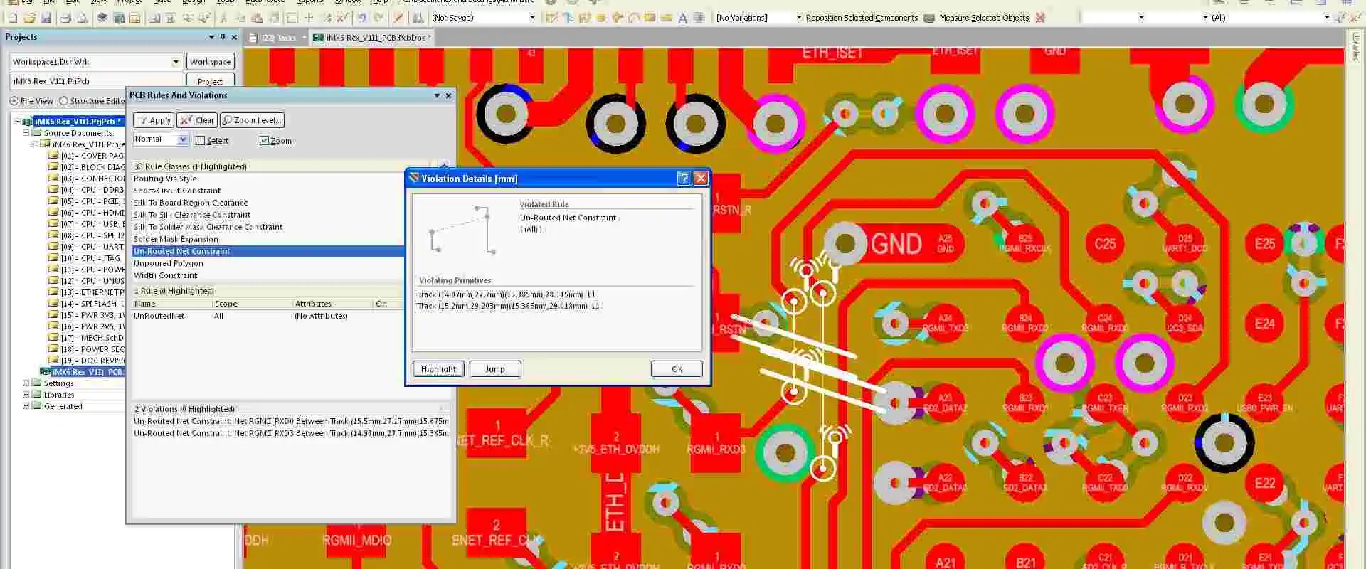
Design and Electrical Rule Check

In addition, KiCad provides a robust DRC and ERC system that looks for issues like conflicts of the output pin, missing drivers, as well as disconnected pins. Also, it features netlist export that enable designers to be able to save all their netlists to take a variety of file types, including XML, Pspice, PcbNew, and Cadstar.

Routing and Layout Using PCBNew

PCBNew enables more efficient and faster routing. This software removes barriers by pushing the forward traces thanks to its great routing features. Alternately, this program can perform rerouting and ignore the obstructions. This system complies with DRC standards.

3D Viewer

Users of KiCad have access to 3D viewing, interactive viewing, as well as the choice to see 3D models in the shape of two-dimensional drawings, making it simpler to comprehend part details.

Cross and open source platform:

KiCad is known as open-source software that permits users as well as developers to improve as well as debug the platform constantly. This means improved features and faster upgrades. Linux, macOS, and Windows systems can all run this program.

Simple-to-use user interface:

This program offers a user-friendly, intuitive interface that makes it simple for beginners to learn design and develop their talents. Because of the tutorials’ emphasis on major tools as well as working speed, its learning curve is simple.

Pros of KiCad

layout
layout
  • The hotkey feature is a great tool for productivity because it enables users to create shortcuts for quick access to commonly used functions.
  • The program’s functionality and range of features are excellent considering that it is totally free.
  • Support for SPICE simulation is offered by Eeschema with the ngspice integration.
  • The partial support function of the clipboard allows for the movement of nets and symbols between the hierarchical sheets.
  • Better preview and navigation features, including cross probing and a capability for custom color choice.
  • KiCad now includes an editor for the environment variable to assist users in managing internal environment variables.

Cons of KiCad

  • KiCad’s library management functions require centralization and development. Working with less or newer prevalent components has reduced part availability.
  • Some earlier KiCad versions may have latency difficulties for macOS users.
  • KiCad does not enable autorouting or quick feature design.
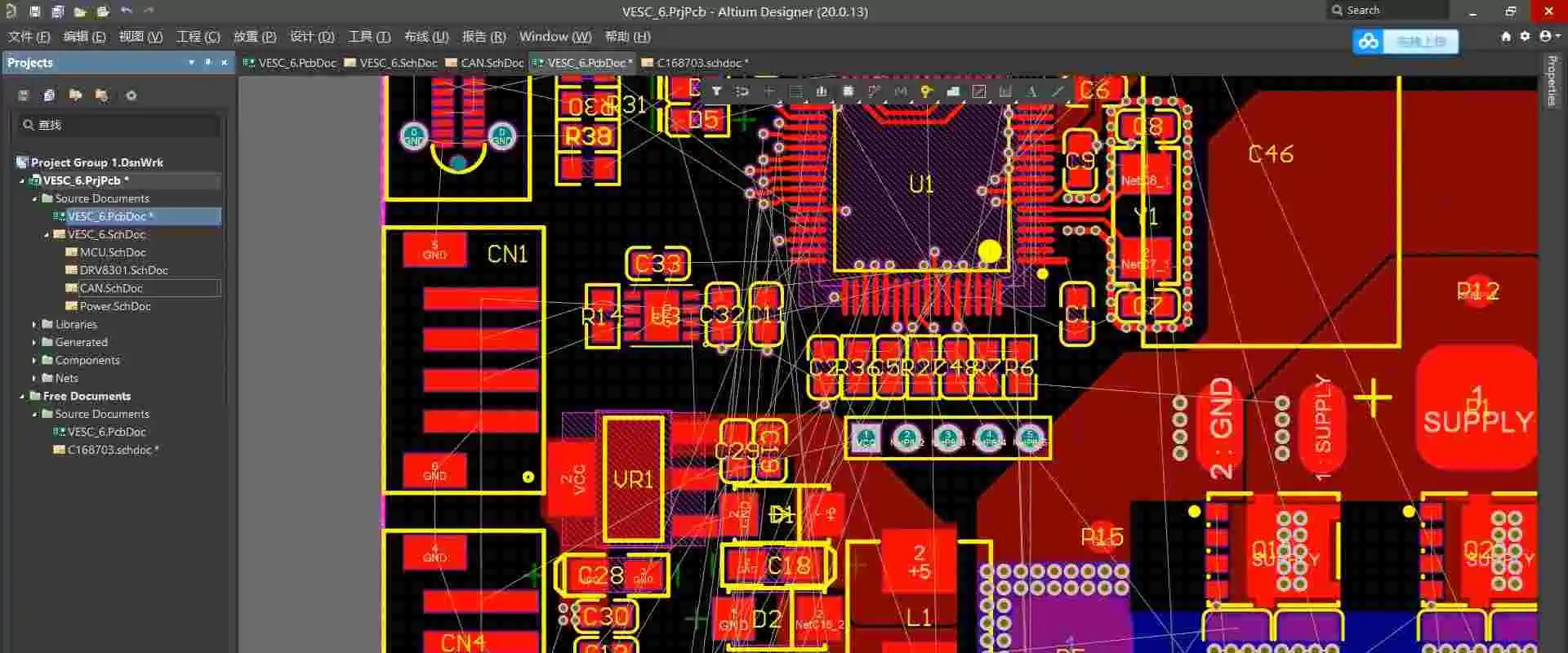
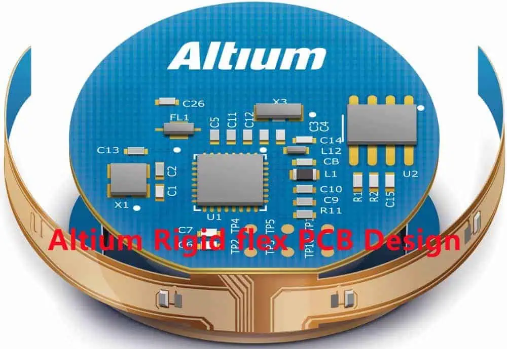
Altium Designer

Altium Designer is a pioneer in the sector of PCB design for the past 20 years. Also, Altium Designer 22 is their most recent version, which includes new enhancements as well as performance upgrades.

This program’s simplicity and sophisticated technical capabilities are combined in an attractive package, which is one of its best features. Within one main software package, the software offers a comprehensive PCB design through to the production solution.

Despite being on the more expensive end of the price spectrum, this has tools for everyone. Even inexperienced users are able to create and carry out projects thanks to its usability, and experts are given access to adequate cutting-edge technologies to work on more difficult design assignments.

These are just a few of the numerous capabilities you’ll discover in this software: 3-D rendering and viewing, a customized user interface, comprehensive format support, as well as content libraries featuring many prebuilt components available for usage.

Additionally, Altium customers receive cloud services, part information relevant to production, automatic and interactive routing, as well as filtering and tuning tools for building high-speed features. To understand more regarding the Altium Designer, continue reading.

What are the Main Features of the Altium Designer?

shows the layout after correcting these three types of errors.

Altium Designer offers 8 major features, which are explained below

Schematic Design

Altium’s innovative schematic solutions, that break down as well as simplify complex models to different single sheets to ensure easy understanding, makes it simpler to work using schematics having complex designs, many sheets, and various layers.

Rule Validation

Using Altium Designer, the designers may use the ERC as well as DRC functionalities to instantly check their circuits as well as routing. This feature operates by flagging any potential electrical and design rule violations and even dynamically predicts possible violations.

Documenting PCBs with the draftsman

For DFM as well as production, and also for institutional and research uses, documentation is crucial. Part drawings, details, component numbers, as well as other information are included in the PCB documentation. Users of Altium can export the production drawings straight to Draftsman documents.

Cloud-based Working Platform

Altium features a cloud-based facility operating remotely to assist members working on big projects. As a result, these team members can collaborate online, in real-time, share information, get work updates, as well as access some project-related data in a safe, secured setting.

Communication Center

Altium members have access to a center of online communication that enables instant messaging, communication tracking, as well as file sharing, which is another fantastic tool geared for companies and businesses. All of this is completed in a safe and practical setting.

Interactive Auto-Routing and Manual Routing

Routing is made considerably simpler thanks to its interactive routing engines, which helps you establish paths for some node-to-node connection, regardless of how sophisticated the design is.

With Altium Designer, you can route round obstacles, and also hug and push, push and shove, and obtain more such capabilities for effective and quick routing.

Large-scale content libraries

With the help of Altium’s special content libraries, you can obtain many pre-built components, information, part details, links, etc. They are conveniently accessible and have more than 400k items that are ready for download. All these are integrated into the software.

Functionality of ActiveBOM

ActiveBOM is a sophisticated tool from Altium that makes it simple for users to create, update, and track bills of materials. It automatically incorporates information from the design and aids in document compilation. The program could also ask suppliers beforehand for information on parts as well as supply-related matters.

Pros of Altium Designer

  • Thanks to Altium’s cutting-edge tuning and filtering tools, designing of high-speed features is made considerably simpler.
  • Management of supply chains is improved and may automatically provide information about production during the design stage, preventing problems later.
  • The UI can be tailored to the preferences of the designer, offering improved navigation as well as shortcuts.
  • Through the incorporation of MCAD and ECAD, it is possible to verify enclosure fit with PBC, which is a great option.
  • When compared to other programs inside its pricing range, Altium’s learning curve is less challenging.

Cons of Altium Designer

  • The license fees are pricey
  • It only works with 64-bit Windows systems; Linux or macOS versions aren’t really available.
  • Furthermore, pre-made bundles rather than need-based custom packages are used to sell licenses.

What makes Altium Designer special?

All user experience as well as requirement levels are catered for by the features offered by Altium Designer. A variety of tools and functions linked to production are included in the program.

Altium will instantly look for alternative compatible parts, which is useful for your project if a specific part related to the design is not readily available.

The degree of customization as well as hotkey editing that it permits is another distinctive feature that makes the use of the software simpler.

Who can Use it?

Altium is ideal for any work related to research, industries with Design for Manufacturing as well as manufacturing requirements, teams working remotely, or even individuals who wish to handle more complex designs and projects. However, it can also be utilized by other designers, essentially anyone who will be able to afford it and find it efficient and easy to make use of.

What is EMI Coating?

EMI Coating

The term EMI coating permits applications that are more flexible in contrast to the EMI enclosures. This is because it can be spray-coated into different insulators, areas, and enclosures.

Different EMI coatings are usually spray coated into the inner part of the plastic enclosures that surrounds the equipment needing excellent shielding effectiveness so as to absorb any harmful RFI and EMI. In addition, the metal links having copper, chromium, or nickel alloys are known as some EMI coating that might be sprayed onto any material or housing to help create the EMI shielding effect.

Furthermore, the suppliers and manufacturers of electronic equipment make use of EMI enclosures in different applications like laptops, CPUs, housings of circuit boards, as well as housings for mobile phones and mobile device manufacturing processes. Furthermore, with CPUs, circuit boards, laptops, as well as similar devices, a good number of problematic EMI usually emanates from an electromagnetic cross-talk present inside these electronic devices.

In addition, different components present on one board could lead to the traveling of EMI across conductive materials and wires, interfering with each other. Also EMI coatings could be sprayed on the wire insulation, interior parts of the integrated circuitsโ€™ small enclosures, as well as circuit boards. This diminishes electromagnetic crosstalk present in the devices.

What Does EMI Shielding and Coating Mean?

EMI-shield-PCB

Electromagnetic Interference shielding or EMI shielding involves a specific process, which permits users to protect any sensitive part from possible issues that may arise as a result of their closeness to different electromagnetic fields.

Also, EMI has the ability to disrupt different devices. This includes Cellphones and military equipment. In addition, it could affect navigational equipment, medical equipment, as well as the touchscreen of tablet computers negatively. However, locating the EMI source could be difficult. This is because it could come from the man-made and natural electromagnetic spectrum and fields. The general rule is that anything that could create electromagnetic field could create an EMI as well.

Issues arising from EMI could range from simple, like temporary disturbance of electrical devices, to very disastrous issues, like the huge data loss or critical failure of the systems. Due to this reason, it is very important that you offer some protection to the sensitive devices and parts from EMI. With EMI shielding processes, you will be able to achieve this.

What are the Methods for EMI Shielding?

You can utilize any of these methods in shielding the parts of your devices from EMI.

Vacuum Metalizing

The process of vacuum metalizing has to do with metal vaporization, with this vaporized metal applied to the surface of a part. We can utilize the vacuum chamber in directing the metal vapor flow that makes sure even coating is applied.

This method needs extensive pre-tooling that permits the preparation of the parts ready for shielding. Moreover, the method permits large-scale manufacturing runs which coat many of the parts. In addition, it is possible to add a specific top coat onto its metalized part. This could enhance the EMI shielding better.

For this process, aluminum can be used. This is due to the fact that aluminum usually forms a specific oxide later all over that part, coupled with making sure there is conductivity where necessary. Moreover, coating of the parts can also be done in silver; although you will have to spend more.

Electro-less Plating

Here, a very complex process is utilized, which allows the application of a specific metal coating onto the part. Also, we make use of this specific process for any rigid plastic part offing low conductivity.

First of all, that part is inserted into a specific acid mixture via a process called etching. The step leads to the forming of different tiny holes across the partโ€™s surface. Then, we take out the part out of your acid bath and then insert it in a specific alkaline solution so as to help restore the neutrality.

Following this, we will apply the catalyzing film into that part and then insert it into a specific solution, which is designed to help speed up the process of plating. Lastly, we then apply nickel or copper plating to that part.

How Does EMI Shielding Work?

FULL PCB MANUFACTURING Quote

The main goal of any EMI shielding as well as EMI coating project is to help in blocking offending EMI, as much as possible. This makes sure that it doesnโ€™t get to sensitive electronics present in the enclosure. In order to achieve this goal, there is a need to use a material that has an extremely high electrical conductivity like aluminum and copper utilized for EMI protection. This electric field present in the EMI becomes absorbed

Furthermore, the EMIโ€™s electric field is then absorbs as it starts driving free electrons into the metal in motion. This essentially converts the electric fieldโ€™s potential energy into a kinetic energy

In addition, in our facility, we make use of a process referred to as PVD (physical vapor deposition in applying EMI shielding in the thin layers. In addition, the layers help in providing the EMI shielding and EMI protection that you seek, excluding the weight. This PVD process is a very great option for coating the enclosures of plastic electronics.

Normally, the designer indicates the plastic enclosure over the metal enclosure whenever they are making efforts to reduce cost and weight of the shielding materials. Thereโ€™s an added advantage, EMI applications through PVD are relatively inexpensive and very scalable. This choice is a great one for production runs of large volumes.

Frequently Asked Questions

Why is Shielding Necessary?

Although, the majority of engineers go ahead to design their circuits having the EMI issue at the back of their minds. Offering the shielding level needed isnโ€™t usually possible. Using some parts could stop the circuits from getting to the appropriate efficiency level. This is why EMI shielding is very important.

Why Canโ€™t I make use of metal enclosures?

This is included among the old methods of the EMI shielding. In addition, metal enclosures are just the way it is. Essentially, they are metal boxes (sealed), which you place a very sensitive component in.

Conclusion

Electromagnetic interference has brought about the emergence of EMI coating and EMI shielding. The ultrasonic coating technology and EMI gaskets are useful too.

Altium vs OrCAD: Whatโ€™s the Difference?

Altium vs Orcad

Choosing the right software for PCB design for the fabrication of your printed circuits is a crucial step for electronics engineers. Currently, there is a ton of softwares for PCB design available online. The best PCB Designing software will be challenging to select from all of the available possibilities.

Anyone interested in the electronics business should use Altium and OrCad. They are currently the most popular PCB design software available. Which of them will you choose to create your circuits with? Which is preferable – Altium vs Orcad?

Let’s get to know them before we decide. As a result, you can decide wisely and receive the best for you.

Altium PCB Designer Altium Ltd. of Australia created Altium Designer, a PCB as well as electronic design software package. It is an all-encompassing tool that enables the design, simulation, and production of electronic goods. 2005 saw the introduction of Altium Designer by Altium, which was then known as Protel Systems Pty Ltd.

Its beginnings can be traced back to 1985, when the business released PCB Protel, a DOS-based tool for PCB design.

Characteristics of the Altium PCB Designer

PCB Layout in Chinese PCB Manufactuer

Supply Chain Management System

You may quickly create a BOM for your projects. There won’t be any misunderstandings with your manufacturer.

From a centralized location, you can easily and quickly view the whole of your manufacturing information. You’ll have more tools at your disposal to produce a successful product. The users will enjoy using this function, which makes tracking easier.

Unified Library Management

Each of the libraries that make up its feature library is a collection of useful models as well as components. Its schematic symbols, PCB footprints, lifespan status, as well as supply chain planning are all centrally located on this sophisticated platform. Users get access to this data as well as collaborative capabilities that can facilitate better project management and product development.

ECAD/MCAD

Integrating ECAD with MCAD is offered by Altium. This functionality now makes it feasible to sync with different CAD systems including PTC Creo Parametric, SOLIDWORKS, Autodesk Fusion 360 or Autodesk Inventor. It was among the elements that helped Altium to be included among the best softwares for PCB design on the market.

Cloud-based Platform

Altium Designer is a development and design application that is cloud-hosted, allowing users to work from anywhere. People can watch it as a result from anywhere as long as they possess internet connectivity. Now, project team members can create as well as update various projects from a distance.

With an Altium Subscription, you get something free called Altium 365. Using Altium 365, users can easily create, collaborate on, produce, and handle all aspect of their project in one location.

Schematic capture

You may quickly document your design using a variety of tools, including design verification, variant management, as well as netlist generation.

Pros and Cons of Altium Designer

FULL PCB MANUFACTURING Quote

Pros of Altium Designer

  • Advanced Management of the Supply Chain
  • Real-time supplier pricing with the ActiveBOM
  • Native3D visualization Check for mechanical clearance
  • centralized data for design with high security
  • MCAD/ECAD partnership that is simplified for merging mechanical design and PCB design.

Cons of the Altium Designer

  • Not everyone may be able to pay the exorbitant price.
  • Periodic complaints of bugs or crashes while working on computers with low spec

What are the Platforms Supported?

  • 64-bit Windows 8
  • 64-bit Windows 10
  • 64-bit Windows 2012
  • 64-bit 2016 Standard Edition Windows Server

Is the Altium Designer Really Worth it?

The product is there for you if you’re a person or company trying to increase production and conduct research or production at industry standards.

Altium includes tools to automate the majority of design activities so you can concentrate on optimizing your design. These features include powerful and quick editors, reduced navigation because of the high integration level, and more.

Professionals can use it due to the advanced features, and beginners as well as students may use easily thanks to its user-friendly interface. Therefore, Altium Designer seems to be the best software to choose if you really can purchase it.

What is the OrCAD PCB Designer?

 Electronic design professionals as well as electronics technicians frequently use the circuit simulation and designing program OrCAD. OrCAD is a unique design automation system which is developed by the software company OrCAD Systems Corporation.

Cadence Design Systems bought OrCAD in 1999 after it was founded in 1983. OrCAD as a program, may be used to create circuit boards and electronic circuit diagrams. It also has the potential to mimic how those gadgets work.

The Core Elements of OrCAD

System for Schematic Entry Using the OrCAD Capture

The tool for schematic entry of an OrCAD Capture is one of the most popular circuit diagram tools in the world and is very effective. It employs flat or hierarchical schematics, which can be organized thematically in accordance with a navigation panel’s functional blocks.

SPECCTRA automatic routing

With the absence of layer limit, the SPECCTRA auto routing feature aids PCB routing. The layout could be affected by changing a number of factors. The OrCAD auto router additionally considers high-speed rules including propagation delay. A board can be routed with some layers if quick feasibility investigations indicate that it is feasible.

Physical Layout Circuit Board Editor:

Creating a Pcb board is significantly simpler in the latest PCB Editor. It is able to generate the physical design using traces, planes, component footprints, and holes using a variety of new automated tools. Rule tests are carried out in real-time so as to make the design ready so that it may be implemented rapidly.

Constraint Manager

The Constraint Manager makes it simpler to assign topologies as well as define rules. It is possible to define rules and simultaneously assign them to several nets based on the hierarchy. Both electrical and physical rules are accepted. Once developed, you can import rules and then apply them to subsequent designs.

OrCAD PCB flow’s PSpice Integration

PCB flow provides PSpice’s core functionality. OrCAD Capture’s tool for schematic entry is useful for building a design that can be used to drive the PSpice simulation. When placing and routing the components, your PCB Editor performs checks on your generated data.

Electrical Rules Check

Utilizing online databases as well as user-defined inputs, the ERC tool enables the designer to immediately discover and correct any mistakes without any need for external setup. Even without a simulation model, an ERC check can be carried out after you are done with the PCB stack-up as well as routing geometry. This allows for the detection and repair/redesign of discontinuities in parallel traces or impedance.

Simulation of Signal Integrity

The default IBIS models or the Cadence models could be utilized for simulation and analysis with regard to signal integrity. By choosing a net inside the schematic, you may conduct a simulation so as to check the signal integrity and prevent mistakes from occurring later in the development process. For the purpose of analyzing its signal quality, the impedance or length can be modified.

High-Speed Restrictions

High-speed signals may be subject to an additional set of regulations. They must adhere to the transmission line design guidelines. These may be specified in its Constraint Manager as well as supported by DRCs during layout. The DRCs can account for variables like min-max length, routing layers, differential impedance, etc.

What Makes OrCAD Circuit Board Designer Special?

Fast and simple schematic designs are offered by the OrCAD Circuit board designer. You may simulate MATLAB/Simulink designs using PSpice and OrCAD. It differs from other applications on the market because of this feature.

Real-Time Feedback assists in maintaining data synchronization between the CAD tools, identifying and fixing mistakes automatically. If the DRC is operational, it will identify and alert when there is any problem with your design.

Also it simplifies the process of comparing and interpreting data between both the canvas as well as the Circuit board editor.

Pros and Cons of Choosing the OrCAD Circuit Board Designer

layout
layout

Pros of OrCAD Circuit Board Designer

  • Interactive Routing enables quick and efficient routing.
  • Using automatic CDIR feedback, design errors can be minimized.
  • easier to build as well as manage shapes when editing and routing.
  • OrCAD has the ability to simulate and open MATLAB designs.
  • BGA Fanout Routing With Auto-Assist
  • Circuit design made easier with the Via Creation function

Cons of OrCAD Circuit Board Designer

  • OrCAD relies on individual programs, and its low level integration makes working on complicated projects a little difficult.
  • Only a few libraries are offered without charge. Older versions lack 3D modeling.

Supported Platforms

The platforms supported includes

  • Windows 7 Ultimate, Enterprise, Home Premium or Professional (64-bit)
  • All Service Packs for 64-bit Windows 8
  • 64-bit Windows 10
  • All the Service Packs for Windows 2012
  • R2 Server Windows 2008

Worth Acquiring OrCAD Circuit Board Designer?

The OrCAD Circuit board designer is an application that is utilized globally in a wide range of industries and applications. OrCAD will offer a practical option if you need to operate on server boards, motherboards, or other sizable tasks.

Additionally, it makes the placement of user component and debugging easy. OrCAD Circuit board designer is indeed a worthwhile option to take into account when choosing software because of its scalability and pricing options.

Comparing Altium and OrCAD

Free Trial

The key feature of Altium would be that they offer a 15-day free trial to all other clients asides students and a license that lasts for 6 months is given to students. Students from all over the world have access to the free online system known as the Altium Academic Program. With this they will gain access to expert engineering and content solutions.

Additionally, you can request OrCAD software’s free trial. Because we may download as well as install this trial version initially, we can try the software and not pay initially. If the program satisfies our requirements, we may then purchase the complete version.

Controlled Impedance and Trace Routing

shows the layout after correcting these three types of errors.

Both programs have a lot of functionality, but they also have some key differences. In comparison to Altium, OrCAD lacks a sizable number of functions for controlled impedance and trace routing.

Integration

Thanks to Altium’s wide selection of these software solutions, you may quickly connect it to any system or product. It is especially useful for large scale jobs and projects because it could be integrated into a variety of different technologies.

An easy-to-use tool for creating 3D models out of data is called OrCAD. Large projects, however, are not a good fit for it due to its limited integration and ability to deal with simple and small projects and tasks.

Libraries

A sizable number of libraries for Altium are offered without charge. With OrCAD, this does not happen. Just few libraries are being distributed without charge.

Student Program at no cost

Students from all over the world can access content as well as expert technical solutions through the Altium Education Program. Students will receive an Altium license for six months. For the time of study, the license has a validity of six months, which can be renewed each six months. Over 200,000 components, design templates, and other resources are available from Altium.

With the help of this OrCAD Program, research teams, teachers, and students can learn how to design but also analyze electronic hardware as well as produce it. Verified students can receive a free OrCAD education license through this OrCAD program.

However, the academic version of OrCAD is only compatible with Windows. Also, there is no support for virtual machines. Only students with legitimate academic email accounts may apply for the program. The license won’t be given out until after 30 days.

Pricing

Although Altium Designer is a bit expensive, you will receive a product with higher value and service. OrCAD offers a perpetual license as well as a time-based license, just like Altium.

Altium vs Orcad – Final Verdict

Which of the two PCB design programs, Altium or OrCAD, is better? They are great tools for designing circuit boards. Altium Designer costs a little more, but you’ll get a superior product with better support and better value. OrCAD is constrained in its ability to produce goods of higher quality.

Because of the unique and distinctive characteristics it provides, Altium Designer emerges as the better and superior product in this Altium vs OrCAD comparison.

Why Electronic Shielding is Crucial in Electronic or Electrical Devices

Electronic Shielding

Electromagnetic Shielding is very crucial in electrical and electronic equipment. To achieve EMI shielding, engineers make use of manufacturing techniques and materials to prevent signals from any form of interruption by external electromagnetic signals. Also, EMI shielding involves preventing signals from disrupting surrounding components.

What is Electromagnetic Shielding?

Electromagnetic shielding involves the reduction or prevention of the electromagnetic field (EMF) in a space with the help of barriers that comprise conductive or magnetic material. Also, electromagnetic shielding prevents radio frequency (RF) shielding.

EMF shielding helps in reducing electromagnetic interference. Also, this shielding can minimize the coupling of electrostatic fields, radio waves, and electromagnetic fields. The Faraday cage is a conductive enclosure that block  electrostatic fields. However, the type of material used, the shielded volumeโ€™s size, and the thickness of the material determine the amount of reduction.

Anytime there is a flow of electricity in a conductor, there is the generation of a magnetic field. The generated magnetic field has a relationship with the amount of power being discharged. Therefore,  devices that need power like transformers and motors will generate fluctuating fields. Also, motors usually come with electromagnetic field. To keep these fields running, they switch at high frequencies.

This is considered a suitable method of generating interference. EMI is the negative impact of these electromagnetic fields on other devices. Also, the interference generates as the fluctuating field traverses their connecting cables. For every traverse, there is a voltage induction which may be small. However, data processing devices need very low voltages to function and the triggered voltages are large. This can corrupt output and input signals.

Why is EMI Shielding Important?

EMI-shield-PCB

Electronic devices and systems can be affected by EMI. For instance, electrical or electronic devices used in mission-critical applications like military aerospace, medicine, and industry need ultimate protection from electromagnetic interference.  There are several causes of EMI and this come from natural and man-made sources.

It is crucial for engineers to understand how electromagnetic energy (EME) can result in interference and how EMI protection works. Understanding the basic EMI awareness helps you design gaskets that offer a good amount of shielding against electromagnetic field in the (RF) spectrum. Radiofrequency waves usually form the basis of radio technology. However, they transfer signals that interrupt with wireless communications.

There are several reasons engineers conduct electromagnetic shielding. However, most common reason is to block electromagnetic interference (EMI) from having an effect on sensitive electronics. Furthermore, engineers use metallic mesh shields to shield one component from having an impact on the inside another particular device.

For instance, there is a metallic shield in a smartphone which shields electronics from its cellular transmitter or receiver. Also, electromagnetic radiation shields help to reduce the amount of radio frequency (RF) energy in mobile phones. The user that might absorb the RF if there are no electromagnetic radiation shields.

Furthermore, engineers recommend EMI shielding to improve the security of air gapped systems. Lack of external connectivity and isolation and are enough to ensure their security. However, evidence has shown that there can be acoustical infection by exploiting the electromagnetic emanations of the sound card of the system. Electromagnetic energy, shielding radio frequencies, external magnetic field, and low frequency magnetic fields are factors to consider in EMI shielding.

The government, military, and financial sectors make use of air grapping. Also, human rights organizations, reporters, and activists that work with very sensitive information adopt these measures.

More Facts about EMI Shielding

There are various techniques and materials used for EM shielding. In some cases, a braid shield or metallic foil may surround wires. This helps in blocking errant EMI from the cased wires. In audio speakers, there is an inner metallic enclosure for blocking EMI generated by the drivers so they donโ€™t have a negative impact on TVs and other electronic devices. It isnโ€™t necessary to use complete continuous enclosure if the openings are much smaller than the electromagnetic waves that need blocking.

Engineers can make use of conductive paints to prevent the electromagnetic fields from networks that escape the originating business. These techniques work in a similar way with Faraday cage, which can stop signal corruption that makes electronics to malfunction.

Also, electronics may feature connections filtered for EMI. The integration of electronic components such as ferrules, grounded wires, and capacitors can reduce the impact of EMI noise. Also, you can minimize interference by simply twisting wires together

EMI Shielding Gaskets

An EMI shielding gasket shields electronic devices from electromagnetic interference. In typical cases , EMI shields components comprise sheets and are available in different shapes that fit electronic enclosures or casings. Commonly used materials include copper, aluminum, and steel. These materials are very sturdy and rigid. However, thin metal sheets have the ability to deform when under the pressures needed for sealing. Metal EMI shields usually remain in their shape once they become deformed. As a result, they may enable leakage to and from electronic circuits.                                                 

Common EMI shielding materials used today include metal foams, flexible metal screens, and metal wires.  Also, you can apply coatings that comprise metallic inks to the internal parts of electronic enclosures. This offers great EMI shielding solution.

Each shielding methods has its own benefits.  However, particle-filled silicone is an effective shielding material has it features the physical properties of silicone rubber and the electrical properties of metal. Metal-coated particles are a great option for product designers who need to offer solutions to various sealing and insulation challenges.  Also, silicone filled with metal  is a good option.

Particle filled silicones offer electrical conductivity, allow environmental sealing in varying temperatures, and as well attenuate EMI emissions. Due to these benefits, ruggedized touchscreens integrate EMI gaskets made of particle-filled silicones. Such EMI shielding gaskets prevent the device from any form of mechanical shock and it is usually soft enough to prevent any interference with the display’s touch function.

The cost of EMI shielding materials is crucial considerations for gasket designers in a wide range of industries.

Conductive Silicones

In some applications, particle-filled silicones are a great option, especially demanding applications. However, the question is that can these conductive elastomers meet the demands of your application? Or are EMI shielding gaskets made of conductive silicones a cost-effective option?

Well, Silicone is a type of material that can withstand water, sunlight, water, and various degrees of temperatures. However, when particle-filled silicone contains more metal particles, they can have negative effect. This is a major reason some gasket designers may reject particle filled silicone that seem too soft or too hard.

Some engineers complained about the limitations of part size as regards long lead times for materials and mold dimensions. Furthermore, a god number of industry experts also claim that all particle-filled silicones canโ€™t support thinner electronic designs since they are too thick. Also, the cost of particle-filled products is another consideration as this discouraged their use.

Silver-aluminum was the commonly used filler material for protecting silicones for several years.  The development of the MIL-DTL-83528 specification of the U. S military contributed to the particle. However, things changed in 2011 when silver cost almost $50 per Troy ounce. The fact that many gasket prints and drawings had these elastomers specified on them became a problem. EMI gaskets that comprise silicones were even more expensive.

Electronic designers now have a cost-effective alternative particle fills that provides very strong EMI protection. Silver-copper and silver-glass are also commonly used. Today, nickel-graphite silicones which are a cost-effective material function at the shielding level of silver-aluminum. According to MIL-DTL-83528, these nickel-graphite silicones meet the requirements for effectiveness of EMI shielding effectiveness. At RF frequencies that range between 20 and 10,000 Hz, the MIL-DTL-83528 requirement establishes a minimum EMI shielding effectiveness of 100 dB.

Electromagnetic Interference (EMI) Materials

FULL PCB MANUFACTURING Quote

Innovation in silicone compounding has turned things around for good. Particle-filled elastomers can now meet the requirements of shielding and as well as other project specifications. For instance, nickel-graphite silicones are soft enough for gaskets since these silicones are available in 45, 40, and 30 durometer. Higher-durometer shielding elastomers can withstand chemicals and fuels. These Elastomers integrate  fluorosilicone as their base. Also, these fluorosilicone compounds are usually available in durometers of 50, 60, and 80 for applications that need EMI gaskets.

Newer shielding materials usually comprise metal filler enough to provide electrical conductivity and effective EMI shielding. This is not the case for older shielding elastomers.  Additionally, these conductive silicones enable cost-effective and efficient fabrication.

Particle-filled silicones canโ€™t be deformed or stretched when cutting gasket. The structural properties of the material offer improved tear resistance and there connector holes are well aligned. Improved tear resistance is crucial factor to consider when it comes to thinner wall gaskets. Also, product designers can give specification on adhesive backing to enable easy installation.

To achieve great shielding effectiveness, particle-filled silicones are ideal for use with electrically-conductive adhesives. This is crucial where Z-axis conductivity is necessary in shielding applications. Also, there are different types of higher-durometer, nickel-graphite silicones available. However, some EMI gasket applications demand for added strength. This is the reason EMI materials feature products like 65-durometer elastomer with an inner nickel-coated mesh.

You can reinforce lower-durometer, nickel-graphite silicones using an inner layer of conductive fabric for improved conductivity and material strength. Therefore, this prevents tearing and brittleness while fabricating EMI gasket. Conductive or magnetic materials are ideal for electromagnetic shielding.

Types of Electromagnetic Interferences

In our modern environment, EMI is very common. There are two major sources of EMI. These are natural and human made source. However, there are several classifications of EMI. Here, we classified EMI in several ways.

Human made EMI

This type of EMI happens from electronic device. Also, human made EMI occurs when several signals go through one device at similar frequencies. For instance, a radio simultaneously picking up two different stations.

Natural EMI

Natural EMI also affects electronic devices. This EMI is considered natural because they are not human-made. It occurs due to natural phenomena on space and earth. Natural phenomenon such as cosmic noise and electric storms are responsible for this EMI.

The second classification is based on EMI duration. The duration here refers to the time it takes the device to experience interference.

Continuous EMI

Continuous EMI occurs when a source keeps emitting EMI. Also, the EMI ย source can either be natural or man-made. This EMI occurs as a long coupling mechanism and it usually exists between the source of and receiver. Also, continuous EMI usually occurs from sources such as a circuit that generates a continuous signal.

Impulse EMI

Impulse EMI is not continuous, they only occur for a very short period. The source of this EMI can be natural or human-made. Examples include noise from lighting and switches which generate signals that could disturb the voltage and current.

The third classification of EMI is simply based EMIโ€™s bandwidth. The bandwidth of EMI is the frequency range the EMI experienced. Therefore, EMI is into two types based on this. These are Narrowband and Broadband EMI.

Narrowband EMI

Narrowband EMI happens at a single frequency. Also, different types of distortion in a transmitter can cause narrowband EMI. Narrowband EMI plays a minor role in the communication system and it is easy to correct this type of EMI. However, it is crucial to control the limit of interference in limits.

Broadband EMI

Broadband EMI doesnโ€™t occur at a single frequency. As regards a magnetic spectrum, broadband EMI covers a wide spectrum. Also, it occurs in different forms. The source of broadband EMI can be man-made or natural. An example of a human-made source is spark that emits from an arc welding.  Sun-outs for a satellite TV system is a good example of a natural source.

How to Reduce EMI

EMI commonly occurs in industries and it results in an adverse effect on signals. A few sources of EMI from industries include Power contacts,  Variable frequency drives, AC and DC motors, Soft start motor starters, Power wiring, SCR heater controllers, arc welding, and more. Therefore, there is a great need to prevent or reduce EMI. Otherwise, EMI will degrade crucial measurement and control signals.

There are three main elements that cause EMI noise. This include a coupling channel between receiver and a source, noise source that produces noise, and receiving device that impacted by noise. Engineers can achieve electromagnetic compatibility (EMC) if they can minimize or eliminate any of these elements. Also, you need to apply very few techniques to get rid of EMI.

Shielding

Shielding is one of the most common techniques of eliminating or reducing EMI. There are a wide range of factors that contribute to EMI. However, there are several ways to reduce EMI. Shielding is one of the most effective ways to combat EMI is through shielding.  Also, shielding is a method that involves reducing and controlling the coupling of electrostatic fields and radio waves.

EMI shield is usually implemented to protect electrical devices from external factors and to separate wires from the environment. Also, there are three main factors that determine the shielding effectiveness. These factors include multiple reflections, absorption, and reflections.

Shielded cables are electrical cables that have insulating conductors enclosed in a conductive layer. The shield can comprise strands of a spiral tape, conducting polymer or braided copper. Also, shielded cables are usually more rigorous and thicker than those that arenโ€™t shielded.  Also, they need more extensive care when working with them.

Unshielded cables canโ€™t reduce EMI since they do not have internal shielding. These cables use a pair of twisted wires to get rid of EMI. Also, these cables are very thin, which makes them the best option for indoor applications in an office.

Shielded cables are usually much thicker than unshielded ones. Also, these cables also need more extensive care.

Earth ground

The ground systems usually carry return currents and signals. Also, they create the references for both digital and analog circuits. Therefore, they protect equipment and humans from lightning and fault. Furthermore, flow of current in the grounding system results in the possible differences.

Lightning causes a possible difference in volts when it strikes. Therefore, it is crucial to consider the ground system from when circuit design begins. Engineers should consider the ground system in such a way that it functions with safety requirements. It is crucial to be sure of where the current will pass through whenever you are troubleshooting a ground problem.

Also, the current might likely not return to the path when different grounds coincide. Furthermore, there are several factors that determine proper grounding. These factors include the impedances and frequencies, safety issues, and the length of cabling required.  

The single-point ground is the most beneficial ground type for low-frequency applications. When there is sensitive circuitry or cabling, avoid the daisy chain or series connection. This is because there is a flow of return currents from three circuits via common ground impedances. Carrier material loaded

Conclusion

Electromagnetic Shielding is very crucial in electrical and electronic equipment. To achieve EMI shielding, engineers make use of manufacturing techniques and materials to prevent signals from any form of interruption by external electromagnetic signals. Also, EMI shielding involves preventing signals from disrupting surrounding components.

Altium Vs Cadence: What Features Do They Offer?

Altium vs Cadence

Time is valuable, so you should design your Circuit board appropriately from the beginning. Making the wrong Circuit board software choice could lead to numerous pointless modifications and a significant delay in your project’s completion. The two most widely used PCB design programs are Altium as well as Cadence. These software tools aid in the creation of effective PCB designs.

What Does Altium Designer Offer?

A PCB design automation tool and software were created by the Australian software company Altium. It is currently the most popular program in the electronic design business. It includes an auto-router, a schematic, and PCB module. It also includes pairs for differential routing. Additionally, it facilitates the turning of the track length and 3D modeling.

It offers a variety of editors as well as software engines for electronic product development. It aids in managing processing, compiling, and editing. This software also provides X2 integration. Since the environment is completely adjustable, one can arrange the workspace to suit the situation.

Features of Altium Designer

  • Turning of the track length as well as 3D modeling
  • Powerful tools that helps in the management of data
  • Helps in cost estimates, and real-time transparency
  • Reuse of the design tools
  • Modern technology for routing
  • Enough intelligence that aids the management of the supply chain

Engineers will be able to save some time by getting access to the entire tools for design all in one spot. This allows them to complete the entire process of design in one simple environment, as well as deliver top-quality products much faster. This is the way that Altium has taken top spot when searching for the most reliable software for PCB design.

What are the Benefits and Pitfalls of the Altium Designer?

Cadence pcb design

Benefits

  • With respect to the design needs, the 3D and the 2D body can be toggled easily
  • Users can work easily with the STEP models
  • Importing the mechanical data in a specific design for the monitoring of a 3D model is possible
  • Helps in the revision of the designs stored earlier, which leads to better productivity of the organization in the designing and development of the PCB design
  • Exchanges data easily with the MCAD systems

Pitfalls

  • For the schematic of medium sizes, its default settings usually generates many specious warnings
  • Startups could be slow because the software is a heavy one
  • Routing designs could be difficult because Altium comes with many constraints
  • Auto-router limitations
  • Less functionalities in contrast to the other programs and softwares

What Does the Cadence PCB Designer Offer?

In a design system that is constraint driven, Cadence PCB Designer swiftly converts basic and complicated designs from conception to production to guarantee performance and manufacturability. Designers can fit all future and present methodological and technological requirements for organizations, teams, as well as projects of any size and complexity on a budget thanks to scalable technology. You may perform high-speed designs, RF antenna, DFM technology, and flex-circuitry with Cadence Allegro Circuit board Designer.

Your cutting-edge and original designs can come to life with the aid of Cadence PCB Design. You can continue designing while receiving real-time visual input from the environment that is constraint-driven, which also guarantees the usability and producibility of the PCBs.

You can make decisions based on real-time designing insights provided by workflows of integrated analysis, cutting-edge routing technologies, as well as a wide range of different design checks.

Regardless of the density, sophisticated routing algorithms make it simple to handle both basic as well as complex routes. Choose from a variety of options in the planner to shorten the routing process, including contour, scribble, slide, any angle, hug, push, tuning, etc.

Without sacrificing quality, Cadence PCB Design’s HDI technology enables you to meet your demands for a small and slim design. This makes it possible to manage electronics miniaturization without the need for a microscope. Reducing the number required for design iterations as well as accelerating the time it takes to put your designs into production is possible by relying on real-time manufacturability assessments.

In order to guarantee manufacturability and successful electronic assembly across every level of the design process, link with the manufacturing rules just at outset of your design to shorten design cycles as well as boost productivity.

Benefits and Pitfalls of the Cadence Allegro

FULL PCB MANUFACTURING Quote

Benefits

  • Allegro comes with auto-interactive commands, which helps in phase and delay tuning. In order to simplify the interface layouts, these overlays are usually color coded.
  • In order to optimize, as well as simulate the design, there is an inclusion of the Keysight ADS
  • The system for Allegro Automation helps in handling the edits of documents consistently and smoothly. These include file edits, drawing details, annotations, and more, which are tracked and easily viewed.
  • With the DFM Technology the manufacturing and design rules could be viewed and checked easily and quickly.
  • Users will be able to set constraints for the customer design, as well as automate the process of checking to be able to get the feedback on the validity of the design.
  • Interconnection routing and planning are easier when working with the interface of high speed for any complex design.

Cons

  • Creating the library symbols could take a very long time
  • Time for setup could be high; also, it has a steep learning curve

Altium Vs Cadence – What is the Difference?

User Interface

An unattractive user interface for PCB design software can be very annoying. You can have a bad experience with things like terrible color palettes. A poor user interface is really a thorn in the flesh. Altium features a great approach to PCB design. Its user interface makes your experience a lovely one. You will enjoy working in the tool in Altium Designer. This is because it feels really great and the choice of color is something you would love.

However, this is not the case with Cadence Allegro/OrCAD as it does not offer users with an enjoyable user experience. The user interface isnโ€™t what you would really like. However, this does not mean this software isnโ€™t powerful or efficient enough. Once you use it correctly, you will enjoy your work, but it’s not an application you will love to play around in.

Altium enhances the experience of the user as the work progresses. However, Cadence Allegro works like a pick up truck that can perform more heavy lifting for you. Also, Cadence is very amazing for work, but it isnโ€™t what you would like for taking pictures.

Help & Documentation

A helpful documentation is necessary in every PCB design software. It serves as a guide. This means it tells you what a thing is and how to use it giving examples. This really saves you so much time. Nobody likes to waste time on things when they donโ€™t know how to do it. A good documentation is really a life saver.

The documentation in Altium Designer offers great context on the reasons you should utilize a feature in the tool. Also, it gives example on how to go about it. However, users have to visit their website to find what they are looking for. Also, users must be sure of the particular term they are looking for. Sometimes you might not know how to describe the particular term in Altium. In this case, you need to go through the categories in the documentation. You may likely come across something that gives answers to the problem. This is not convenient to do in Altium.

 Allegro/OrCAD makes this more convenient.  When you click the ‘Help’ button in the window you are working in, the documentation brings out what you need. Also, Cadence Allegro allows you to learn the terms of those features. Also, it provides examples on how you can use them.

Ease of Use

Ease of use can be classified in two different ways. The first is, how you can easily integrate the rule manager. Secondly,  how easy can users apply rules for the circuit board. It is much more intuitive to set up rules in Altium Designer than it is in Cadence. But, there are more considerations to take when applying the rules. This includes having to script/code a rule and managing rule priorities.

The constraint manager of Cadence Allegro is no way intuitive to use. This is because this feature requires some training or tip. You can easily make rules once you understand how the tool works. ย 

Efficiency During Design

You need a constraint management system/tool that doesnโ€™t require you to keep updating. Once you set up a constraint management system, you donโ€™t need to update it.  

Altium Designer is a perfect software that works excellently when making constraints that make intuitive sense. The graphics and images are useful and helpful along the way. However, once you work with any high-speed design, you will need to include a code to help manage some differential pairs, constraints, net classes, etc. After this, you can now set the priorities.

However, this isnโ€™t the case in Cadence Allegro. Everything is completely different.  The constraint manager enables  you to create several constraint sets. You can assign these constraint sets to any group of your choice. This is a simple and efficient method to set constraints. Another great thing  is when you can change a constraint for any object in your design  without code. However, you can still set some special constraints using code.

You need to be very careful of the Constraint Manager tool in Altium designer, especially the constraints is set for certain boards.  In cadence Allegro, all you need is to set it from the top level to the ground level. This makes it very effective.

Reliability

Reliability is one of the most crucial benefits you need in any EDA software. The ability for users to trust that  the software won’t make mistakes while working on their PCB project is a great assurance. This is because errors can be a nightmare for you as you will need to spend your precious time fixing those errors. Not only the time involved, the effort involved in correcting errors is exhausting.

The rule management of Altium Designer is indeed a great feature that helps you to keep your design in check. But, there is one major concern for users. This is the number of custom rules users need in  creating with code.

Cadence Allegro is really a reliable software as it changes the whole story. Users can see everything constrained by simply integrating the spreadsheet-based approach to rule management. Furthermore, the sets-based  group-based approach of Cadence to constraint management  is very simple. This approach is very effective and powerful.

Also, Cadence Allegro allows you to set certain parameters on every net. However, the rule management system of  Altium requires you to create it and always come back to check.

Custom Constraint Regions/Areas

Most PCB design software allows you to set any region on the circuit board with.  Altium Designer makes it easy to design custom constraint areas/ regions. All you need to do is to build a Room object, then place it on the printed circuit board and design a new rule set that defines where the rule is applicable.

Cadence Allegro features Constraint Region boxes that allow users to design a custom rule area. Also, users can place that region in a ‘Constraint Set’. The two methods are very easy to carry out. However, ย the OrCAD’s method is preferable since it allows you to reuse the special region constraint set any time you want.

Which of the Them Suits You?

Job Seekers

Cadence Allegro is a reliable option if you will be working in any Corporate Industry. It is very difficult to see a large company, which doesnโ€™t talk about the Cadence Allegro software whenever they mention Altium.

College Students

Students in the college ought to learn how to use Cadence or Altium. Usually, the industry desires freshly graduated engineers that know how to make use of the software.

Conclusion

By now, the features and differences between Altium and Cadence are very clear. Work with whichever suits your work and projects.

Features and Applications of L Band Patch Antenna

L Band Patch Antenna

There are various designs with different operating frequencies, dimensions, and gains to choose from in order to meet different requirements and applications. The L band patch antenna is specially designed to receive L-band satellites like GPS, Iridium patch antenna, Inmarsat, and other types of satellites that offer transmission between 1525 โ€“ 1660 MHz.

What is L-Band Patch Antenna?

The L-band patch antenna is a type of antenna specially built for several GNSS bands. Also, it is suitable for Inmarsat and Iridium telecom applications. Also, this patch antenna is made up of metal and strictly designed for low-cost, robust applications. It is suitable for use in high-power applications. The removal of  substrate loss has allowed the provision of high antenna radiating efficiency.

What are the Key Features of L band Patch Antenna?

L band patch antenna comes with a lot of excellent features which include:

  • Low PIM design
  • Very robust and it is specially made of metal
  • They have a wide frequency bandwidth
  • Also, these antennas offer high gain and high efficiency
  • They cover multiple GNSS bands such as G PS L1,
  • These antennas cover Inmarsat and Iriduim bands
  • They feature circular polarization

There are various designs with different operating frequencies, dimensions, and gains to choose from in order to meet different requirements and applications. The L band patch antenna is specially designed to receive L-band satellites like GPS, Iridium patch antenna, Inmarsat,  and other types of satellites that offer transmission between 1525 โ€“ 1660 MHz.

It is important to know that the L band patch antenna is not ideal for weak signals that need a dish such as GOES. The L band patch antenna features a set with a large suction cup. Also, it features bendable tripod and 3M RG174 extension cable which helps in installing. This antenna comes in a weather proof enclosure. Receiving l band satellites

What is L Band Antenna?

L-band is simply a defined frequency range from 1 GHz to about 2GHz in the radio spectrum. Also, the L band is widely integrated for satellite communications, Global Positioning System (GPS), Radars, Telecommunication, and Aircraft surveillance.  This band features a very small bandwidth since it ranges from 1 to 2 GHz and as such, L-band is commonly integrated in fleet management and tracking systems.

Due to the low profile, wide applications, and easy fabrication of patch antennas, these antennas have become very popular in space crafts, aircraft, and satellite communications. Even in wireless communication, there is an increase in protocols you need to fully integrate in a single device. Also, you can easily achieve this by integrating single-band antennas for every required application. Also, you can integrate a multiband antenna which has similar structure and size of a single band.

Furthermore, multiband antennas are ideal for use in devices that need to cater for some protocols. Also, multiband antennas require to use expensive filters to help suppress unwanted signals. Therefore, this increases the cost.

Furthermore, reconfiguration is usually considered an alternative technique that gives the same space like multiband antennas.

What are the Functions of a Patch Antenna?

A patch antenna is a usually an antenna that has a low profile. This antenna can be installed on a surface. Also, it comprises any geometrical sheet or “patch” of metal, attached over a ground plane. This ground plane is very big piece of metal. Also, a patch antenna is a type of microstrip antenna.  The two metal sheets when combined create a piece of microstrip transmission line with about one-half wavelength of the radio waves.

Furthermore, the radiation mechanism comes out from fringing fields. There is a radiation at the edges. This radiation makes the antenna to function a bit larger than its physical dimensions. Therefore, you can make the antenna resonant.  To achieve this, the microstrip transmission lineโ€™s length must be a bit shorter than one-half the wavelength at the frequency.

Also, the patch antenna is primarily practical when it is at microwave frequencies. In this scenario, the wavelengths are very short, which makes the patches small. Patch antennas are ideal for use in portable wireless devices. This is because it is easy to fabricate these patch antennas on printed circuit boards. Microstrip antennas refer to multiple patch antennas on the same substrate. These antennas can help in making high gain array antennas. Also, you can achieve phased arrays using these antennas. In phased arrays, ย you can electronically steer the beam.

L Band Satellite Frequency and Satellite Communication

FULL PCB MANUFACTURING Quote

Band frequencies reduce distances when it comes to communication. Band frequencies play a huge role in communication. We can maintain that satellites are usually arranged throughout the space.

According to a principle wavelengths feature various properties. To have a better understanding, let us cite an example.  Long wavelengths have the property it takes to travel long distances and pass through several obstacles they find, like mountains and buildings. However, it is important to understand that higher the frequency results in shorter the wavelength. Therefore, it will be much easier to prevent the traffic of the waves.

There is another crucial situation we need to look into. This is regarding when there are high frequencies, even more than tens of gigahertz. You can imagine that the objects we consider small and simple like raindrops or leaves can stop the waves. Therefore, this results in a well-known phenomenon known as โ€œrain fade.โ€ You can overcome this phenomenon which by applying more power.

A solution to satellite problems

Most times, we only discuss the advantages offered by high frequencies such as the Ka Band and Ku Band. Ku and Ka Band have great features. These bands enable transmitters to give out more data per second. The main problem with such high frequencies is that they may carry more information, however they are in need of more power to prevent any blockages.  Furthermore, this and bigger antennas indicate that there is a great need to acquire more equipment.

There is a solution to this problem. The L Band offers great benefits in satellite communication. These include offering much more stable global operations. It does this even when there are adverse weather conditions in complicated areas. Also, another benefit of this band is that it offers a global network coverage without any form of interruptions. Therefore, this allows mobile users to have access to broadband communications anywhere around the world.

What are the applications of the L-Band?

The L-band antennas are one of the most used frequency range in various satellites worldwide. Also, the antenna offers the advantage of being lightweight. Therefore, the L band satellites are primarily utilized for mobile and tactical operation. Other of its applications, are given in different systems, which includes search and rescue operations. For example, the SARSAT/COSPAS, Russians and Americans used some meteorological satellites. This band is suitable for the downlinks available in satellites having high resolution.

Frequency range in which Band L operates

The L band satellites function in frequencies that from 1,530 to 2.7 Ghz. It is one of the satellites bands that has the lowest frequency. Since the L band has the lowest frequency it is commonly used in the market. One of its benefits includes a longer wavelength. Due to this, external factors such as rain donโ€™t affect this band. If at all such happen does, normally integrated by the Ka and Ku frequency bands.

How to Develop an L-Band ground station.

Building an L band setup is the fastest and most efficient way to start with satcom ACARS. Also, the L-Band is usually around 1.5GHz. There is a broad signal footprint from each Inmarsat. Therefore, you donโ€™t need antenna tracking. All you need to do is to point it at the satellite orbitโ€™s middle. Then, you can receive the signal and as well decode ACARS messages.

One of the most crucial things you need to understand about how L-Band operates is that you will need to pick up the ACARS messages from ground support staff to the aircraft. Most times, L-band is described as land while C band is cockpit.

Buying the hardware

The RTL-SDR v2 patch antenna is the most popular option people settle for when buying an L band.  Other alternatives are usually smaller antennas and this is not recommended.  This is because small size antennas offer low performance and this means very low signal. Some people have tried out the modified GPS antennas. These antennas are too small and canโ€™t be of real value. In fact, avoid any of the small sized patch antennas regardless of how attractive the price is. Small sized patch antennas are often available at a much lower price.

The V2 antenna is a great option worth considering. If you only want to listen to voice calls, then the V2 patch antenna is a great choice. You need more gain for consistent decodes of the audio. One fact is that an antenna is more directional if it has more gain. The V2 antenna is a quality item that offers good properties.

Sometimes, your active L-Band antenna might have so much gain. In this case, the satellite orbit may take your antenna off your sweet spot. All you will have to do is to move every time you need to decode some voice messages.

Conclusion

Due to the low profile, wide applications, and easy fabrication of patch antennas, these antennas have become very popular in space crafts, aircraft, and satellite communications. Even in wireless communication, there is an increase in protocols you need to fully integrate in a single device.

What Is High-Frequency Shielding? A Detailed Guide To Emi

high frequency shielding

Introduction

The electromagnetic properties of soil are associated with chemical and physical variables. Magnetic susceptibility, dielectric permittivity, and electrical conductivity are the common EM properties. The chemical and physical variables include density, moisture content, and soil salinity. They are measured noninvasively by electromagnetic induction sensing. Transmission and receiving coils get separated by an intercoil distance.

And they are proportional to the soil investigation depth. Also, they are the main components of most EMI-based soil sensing devices. They have a frequency band below three hundred kHz. And are receptive to changes in magnetic susceptibility and electrical conduction. HFEMI sensors work between three hundred kHz and thirty MHz. Because of their increased sensitivity to changes in dielectric properties and electrical conductivity. They provide more detailed insights into soil parameters.ย 

What is High-Frequency Shielding or RF Shielding?

  • High-frequency fields are defined as magnetic and electric fields. They have a frequency greater than 100 kHz and less than 300 GHz.
  • An antenna often emits electromagnetic fields of high frequency. They travel at light speed in free space. It allows them to deliver information and energy over vast distances.
  • Field strengths decrease exponentially with distance from the transmitter. When you double the separation in free space, the power flux density will drop to a quarter of what it was.

High-frequency magnetic and electric fields have a frequency between hundred kHz and three hundred Gigahertz. Electromagnetic fields are also known as magnetic and electric fields. This is because of the strong coupling between them at high frequencies.

The electromagnetic fields’ wave nature is describable by the relationship between wavelength and frequency. This, in turn, is relatable by the speed of travel (that is, the light speed in free space). In general, wavelengths are smaller for higher frequencies and larger for lower ones. When sending signals over empty space. The wavelengths can be anything from 3 kilometers to 1 millimeter.

In today’s communications, high-frequency fields are used.

An antenna often emits EM fields of high frequency. They travel at light speed in free space. It allows them to transfer information and energy over great distances. The most common application of this quality is in contemporary methods of communication. They include:

  • Broadcasting, Video, and Wireless Technologies
  • The development of wireless communication technologies. For example, wireless phones and WLAN have made this possible.

The Bluetooth radio modules are an example of a short-range gadget. They employ high-frequency EM fields.

Because of the wide range of uses for HF electromagnetic fields. Modern humans are constantly bombarded by a vast range of transmitters. The field strength or intensity is either specified as follows:

  • Measured in volts per meter (V/m) or amperes per meter (A/m) for electric fields or amperes per meter (A/m) for magnetic fields.
  • In terms of power flux density (measured in watts per square meter, W/m2).

The strength of a magnetic and electric field is multiplied to determine the power flux density.

Propagation of High-Frequency or Electromagnetic Shielding 

Field strengths decrease rapidly with separation from a transmitter. Power flux density in open space drops quadratically with distance. And halving the distance results in a one-fourth reduction. The intensity close to the transmitter might vary greatly. Even at constant distances from the source. Because several antennas, by virtue of their design, emit in different favored directions. Thus, it is impossible to determine the field strengths at a specific site from a distance only.

When high-frequency EM fields encounter obstacles in their direction of propagation, they might get absorbed or reflected. The material characteristics of the object have a specific role. They are important in determining which mechanism is dominant. As a result, the transmission of HF fields in natural settings is very different. When compared with the simplified situation described above. That involved transmission in free space.

RF Shielding

HF electromagnetic fields get reflected by conductive or magnetic material, such as metals. HF electromagnetic fields can be totally or partially shielded by materials. The materials can be metal mesh or foils, as well as metal-coated glass panes (for heat retention).

Significance of Electromagnetic Interference Shielding 

Every designer and engineer working with electronic circuitry must consider electronic shielding once its nature as electromagnetic interference gets understood. Its potential consequences on its immediate environment become readily apparent. Touch or conductive EMI. Close or without interacting (capacitive and magnetic EMI) and radiating EMI (which travels further) can all have an effect on electronic devices.

Due to technological progress and the widespread use of electronics in today’s digital age. The EM wave spectrum has become severely oversaturated. This includes electric transmission and distribution system-related disturbances. As well as those caused by external factors like lightning and solar flares.

High-Frequency Electromagnetic Shielding Effectiveness

  • signals received by communication equipment get distorted or jammed
  • Total destruction or breakdown of the electronic system
  • Power surges, spikes, and surges, as well as EFT or quick electrical changes
  • Shocks and burns from electricity
  • electrical systems have decreased efficiency and shelf life
  • Probably Ignition Source

To solve these issues, international groups have stepped in to create EMC, or electromagnetic interference, standards.

EMC refers to the ability of some devices to perform normally in an electromagnetic environment. There shouldn’t be any electromagnetic energy production or transmission to other devices, either.

The CISPR, which is a member of the IEC, and the ISO establishes global EMC regulations.

EMI Shielding Mechanism

FULL PCB MANUFACTURING Quote

EMI shielding is the other practical method of implementing EMC. Alongside filtration, grounding, and bonding. This process involves building enclosures with the proper EMI-shielded material thickness, shape, and structure to redirect EM waves (either into or out of the equipment). When electromagnetic waves pass through conductive or ferromagnetic materials, their path gets modified by reflection or absorption.

Magnetic and electric fields are the two main components of electromagnetic waves. The two components are in phase with one another and move at the same speed. The electric parts of a printed circuit board (PCB) or electronic circuit device get shielded by the conductive substance. At the same time, the magnetic components get shielded by the strong magnetic permeability feature, however, because electromagnetic waves have a complement. Shielding one component safeguards the other.

Multiple reflections, absorption, and reflection are the three methods that can be used for EMI shielding.

Reflection

The EMI shielding system is the primary defense against electromagnetic interference. The electric component of electromagnetic interference gets dampened via reflection. However, mobile charge carriers in the material become important to achieve EMI reflection. This necessitates a conductive quality in the RF radiation shielding used for protection. Within the conducting shield, EM waves interact with mobile charge carriers. It causes the carriers to redistribute their charges. And generate an opposing EM field.

Due to the redistribution of charges, an electromagnetic field gets produced. It cancels out the external magnetic field. This method works. Because the properties of a shield improve with the conductivity of the material. Discontinuity is an important part of the mechanism’s design flaws. The shielding qualities of an enclosure get nullified. If the size of any hole or other discontinuity in the structure is greater than the wavelengths of the external EM field. Hence, it’s important to keep these dimensions as small as possible. While designing the enclosure. To combat stronger EM waves. Where shrinking the hole size would be futile, filtering tools can get used.

Another difficulty is the skin effect, which is more noticeable in AC circuits. It involves the buildup of charges on the surface of a conductor. The charges build up due to the passage of alternating current. As a result, there is now a higher concentration of electrical current in this region. The shielding effect and conductivity are both reduced. Since the inner segment of the conductor gets used less. Higher-frequency electromagnetic waves are more prone to this impact. Consequently, the solution is to expand the surface area of the conductor. It, in effect, expands the region’s usable cross-section. Electroplating the surfaces with conducting materials is another option. Silver or Copper can be the possible options.

Absorption

It is a method for blocking electromagnetic interference (EMI), particularly its magnetic component. The presence of electric and magnetic dipoles is necessary for EMI absorption to be achievable. These materials are notable for their high dielectric constants and magnetic permeabilities. When an external magnetic field is present. The magnetic field lines cutting through the material get disrupted. A magnetic field line can get absorbed by a container with this property. It is possible by following a path within the structure that maintains itself. However, low conductivity is a frequent issue that arises from their use. As a result, their ability to shield or safeguard electrical components degrades.

The attenuation of the incoming EM waves by the phenomenon of eddy currents is a crucial part of the absorption process. It reveals itself anytime there is a high-frequency oscillation in the electromagnetic wave. As a result, it causes the conductor’s internal currents to get induced. Their magnetic field’s eddy currents act to counteract the external field’s strength. It’s also true that eddy currents in materials with electric conductivity tend to be more robust.

Multiple Reflections

It is another mechanism discovered to predominate in compounds with large absorbent features on their surfaces or interfacial areas. Multiple reflecting barriers that reflect the EM waves serve to block out the RF radiation. As a result, the EM waves get dispersed.

Materials Used in High-Frequency Shielding 

Understanding the two basic EMI shielding qualities, electrical conductivity and magnetic permeability, is essential. It is important for thorough consideration of EMI shielding materials. It’s a relief to be rid of them, given their existence was established and discussed in the prior section. However, submitting a query to RayMing PCBs and Assembly can also be useful for such components. If you’re looking for ways to protect your electronics from EMI, this company has you covered.

The question then becomes, what materials can be used for EMI shielding?

ยท       Metals

As a simple and inexpensive EMI shielding option, it is a no-brainer. Metal is an excellent EMI-protecting material because of its nature and qualities. For example, strength, ductility, electrical conductivity, and magnetic permeability. For attenuating electric fields, silver is the most effective substance. Because of its high electrical conductivity and resistance to corrosion. Silver has a high value, but it is also very expensive in comparison to other EMI shielding materials. Therefore, silver is generally used as an electroplating coating or alloy component.

Therefore, silver is generally used as an electroplating coating or alloy component.

Copper and aluminum are the industry standards. Because they provide adequate shielding at a reasonable cost. The electrical conductivity of Copper is identical to silvers. But aluminum’s is 40% lower. Electromagnetic radiation can be effectively blocked by carbon steel. It may include carbon steel or ferritic stainless. Also useful as magnetic shielding materials are the alloys of iron-nickel, such as Permalloy, Superalloy, and Mu-metal. Mu-metal is the most popular, and it is also the most permeable, making it the most abundant.

ยท       Carbon Allotropes

It stands for the class of carbon structures. It includes carbon fibers, carbon nanotubes, graphite, and exfoliated Graphene. Composites containing such allotropes are usable as EMI shielding agents. Its inherent strength and conductivity make it a useful material. Furthermore, they rely heavily on a shielding technique involving multiple reflections.

Because of its adaptability and its ability to flow over the surface of the sealing areas, exfoliated graphite is widely used as an EMI-protecting gasket. All the allotropes are porous structures, which aid in the reception of EM noise. The extremely high aspect ratio of Graphene, carbon nanotubes and carbon fibers makes them useful as fillers. Cement, metals, polymers, and ceramics get strengthened by embedding the fillers into their structures. But due to its smaller aspect ratio and skin depth. Graphene and carbon nanotubes are primarily useful for HF shield applications. Therefore, at gigahertz frequencies, these materials are superior conductors to metals.

ยท       ICPs

It stands for a family of unusual polymers that may conduct electricity without any conducting components included. The popularity of ICPs rises due to their low weight and ease of processing. Because of their atomic structure, which includes conjugate bonds. Polymers that are intrinsically conductive can transmit electricity. Because of this, the free electrons can get used to charging devices. Changes are also possible to how well ICPs conduct electricity or carry a current. This sort of change is achievable through undoing or doping.

Although ICPs have been in use, the concept is continually developing. Challenges in mechanical and chemical stability exist. Despite this, they continue to be favorable as primary constituents, notably in carbon nanoparticle and filament-based composites.

What are High-Frequency Shielding Materials? 

Different EMI-protecting materials are typically made from one of three different metals. When searching for the optimal EMI shielding option, engineers may often combine materials.

ยท       Pre-Tin Plated Steel

Some metals used for EMI shielding can block frequencies up to several Gigahertz. But, pre-tin coated steel is very inexpensive. Besides this, it is very effective at blocking frequencies. The frequencies range from kilohertz to low Gigahertz. When compared to the other metals, carbon steel’s low-frequency protection properties stand out. Furthermore, it prevents the steel from rusting and corrosion.

ยท       Copper Alloy 770 / Nickel Silver

Alloy 770, a copper alloy, goes by a few other names as well. Zinc, nickel, and Copper are their constituent elements. The best reason for its widespread use is its resistance to corrosion.

As an EMI shield, copper alloy 770 excels from the mid-kilohertz to the gigahertz band. Its permeability is one, making it perfect for use in MRI machines without the use of magnets.

ยท       Copper

There is a distinction between Copper and copper alloys 770. Copper is the greatest EMI-protecting metal. Because it effectively dampens both electrical and magnetic waves. Copper is present in anything from complex medical devices to inexpensive personal computers because of its ability to block electromagnetic interference.

Copper is more expensive than most other alloys, including unplated steel. However, it has a greater conductivity rate, which is what makes it so useful as an EMI shielding.

ยท       Aluminum

Aluminum is a good EMI shielding material. This is due to its higher conductivity and lightweight. Aluminum’s conductivity is about 60% lower than that of Copper.

But there is a drawback to using aluminum. It has higher oxidation characteristics than other metallic materials. Also, it erodes more quickly. When metal gets oxidized, its strength and durability get compromised.

ยท       EMI Shielding Gaskets

Sealing the gap between 2 flat surfaces is what gaskets are for. Similarly, EMI-protecting gaskets prevent electronic components from getting damaged by electromagnetic interference.

In the past, EMI shielding was achievable by having metal sheets custom-cut. The custom cut was possible by fabricators to fit into cases. Steel, Copper, and Aluminum sheets of suitable thickness get processed in this manner. The circuits they have intended to shield will leak if the sheets get deformed by time or weather and remain in that shape.

The EMI gaskets are composed of particle-filled silicones. And resemble a ruggedized or sieve touchscreen. These gaskets can withstand both hot and cold temperatures. This makes them a great option for dealing with EMI issues.

On top of that, they are simple to make and do not require expensive components.

ยท       EMI Shielding Film And Foil

There is a market for a variety of EMI shielding materials, including foil, film, and tape.

Different forms of EMI materials exist. Conducting silicones, for instance, can get installed as window films. The installation helps to protect electronics from harmful electromagnetic radiation.

The frequency range and electronics getting shielded are the two factors to consider. They determine the EMI protection’s material and shape.

To prevent electromagnetic interference, technicians wrap equipment wires in metallic foil or braid. Coaxial cables are another option. Because they incorporate EMI shielding into the actual wire design, wire bundles can get encased in foil. And cable braids can cover an entire building. Both of these are common practices for technicians.

Connectors are also shielded from electromagnetic interference (EMI) by foil or braiding connected to metal coverings.

The shielding for a PCB consists of a metal enclosure. It is placed over the sensitive components and a ground plane. The technicians then set up a Faraday cage around the sensitive components.

The electromagnetic interference (EMI) from popular household appliances like televisions and microwaves get blocked by the inside steel casing of audio speakers.

Use magnetic materials and conducting points when the frequency of the magnetic field is less than a hundred kHz. Metal foam, metal sheet, conducting polymers, and metal mesh screening. These are some of the other tools used by technicians.

Foil tapes designed specifically for EMI protection have a number of desirable properties. They are both flame and corrosion-resistant. They are flat and engraved, making them easy to mold into unusual configurations.

Shielding tapes can be found from a variety of sources:

  • Connector and cable grounding plates
  • Computer keyboards
  • across the space occupied by separate electrical parts and connections
  • Wherever there are cracks or openings in a protected chamber.
  • Electro-Medical Equipment
  • Electronic enclosures panels and doors
  • The periphery of electrical components like relays and coils that might get attracted to wideband EMI signals
  • Used to shield relays, coils, and other devices from emitting harmful levels of broadband EMI

ยท       EMI Shielding Foam

Carbon foam is another form of EMI protection that is becoming increasingly popular. Even though it contains no metal. The EMI-protecting foam is effective from a hundred MHz all the way up to twenty GHz. Because of its adaptability, foam excels as an EMI shield medium. It’s not just one of those useless things.

Some types of foam, for instance, are used to prevent fires. It is resistant to corrosion. Also, it is lighter in weight than metal and has a longer service life in extreme conditions. In addition, it has a low impact on the natural world.

ยท       EMI Shielding Silicone

Silicone is non-conductive to electricity. In contrast, metal embedded in silicone produces a conductive substance. It is useful as an EMI shielding.

Silicone has additional benefits, like its malleability. Die cutting allows manufacturers to make a custom EMI shielding solution. They can make customized solutions for every application. EMI-protecting silicone has found applications in different departments. These include satellite communication, aerospace, automotive, and electronic device manufacturing sectors.

Silicone is well-liked by many because of its resistance to moisture and light. It is also temperature resistant. Therefore, silicone is used in fields like aeronautical engineering, where temperatures can fluctuate.

Present-day EMI shielding silicone contains nickel graphite. It efficiently blocks RF between twenty and ten thousand Hz.

Where To Find Industrial Circuits – A Comprehensive Guide

Subcontract PCB Assembly

Industrial circuits are the backbone of the enthusiasm for Far Cry 6. We are going to have a look at different aspects of industrial circuit procurement in the game. Besides all the methods, you can gain the industrial circuits in the game. 

What is the meaning of Industrial Circuits in Far Cry 6?

Industrial circuits are important for the weapons in Far Cry 6. These are for the weapon upgrades as well. The players would acquire the industrial circuits after surpassing different game levels. The game predicates the resolver weapons on the whole. The player should use the Supremo in a suitable way to acquire these with the least effort.ย 

Where to Find Industrial Circuits? 

Trading Animal Meat

The exchange of particular animal meats or alpha meats can be executed for the industrial circuits. There are specific locations for this trade. You will acquire 6-7 industrial circuits on one exchange of the alpha animal meat. The offered alpha animal meats are: 

  • Alpha Coyote Meat
  • Alpha Crocodile Meat
  • Alpha Jaguar Meat

Find Alpha Animals

The alpha animals would be present on the hunting grounds so that you can find them easily. Look for jaguars, crocs, and coyotes. The players must kill these alpha animals by the acquisition of industrial circuits. Either use a bow or a knife for seamless hunting. In this way, you will get the alpha animal meat with a perfect strategy. 

Execute Ambushes

Look out for the ambushes. There are four sectors of Yara mainland that come with different ranks. The mainland sectors that have the highest rank would be including more ambushes later. So these ambushes would get you more industrial circuits. Let’s learn about these mainland sectors: 

  • Madrugada: Aguas Lindas
  • Valle de Oro: Barrial
  • El Este: La Joya
  • Esperanza: Esperanza

Open Guerrilla Caches

After entering your first guerilla camp, the players can have a look at the construction desk and camp facilities as well. These are important for the procurement of the Dani and Libertads. Another important factor is the hideout network. You can also procure industrial circuits from this hideout network. 

  • Buy the hideout network and get hideout access beside Yara for fast traveling. 
  • The players can also check the locations of the chief scout present in the hideout network, but this factor is not an essential one.
  • You can reach the appropriate hideout network so that it will position the guerrilla cache on each hideout you encounter. Also, you need to invest your resources in this pursuit as well. 
  • You can restock the guerrilla cache every 24 hours when needed. 
  • Teniente, Guerrilla Caches offer less amount industrial circuits. 
  • Each Guerrilla Cache can be used at all the hideouts in order to procure more industrial circuits from them. 

Industrial Circuits Farm in Far Cry 6ย 

FULL PCB MANUFACTURING Quote

Lola would reward the players with money after the completion of each of its operations. There are solo challenges also available as side operations, but they are simple to complete. The players would also get valuable resources as well. You can procure the Monedas from the insurgency mode. However, it’s not effective to procure industrial circuits. The insurgency mode will be activated after you pass the main campaign level. 

Alpha meat in Far Cry 6

Trade meat can be obtained from alpha animals that are coyotes, jaguars, and crocodiles. The hunting would only include non-ballistic tools like a knife or an arrow. Any other tool would ruin the meat making your efforts go in vain. The issue can be solved by upgrading the lodge to get a buff that will help you with this problem. It would be wrong to say that you only need to aim for industrial circuits. Uranium and plastic items are important too. These would help you with Castillo’s army battle. 

Trade With Lola’s black market

Lola is a good trader to do business with when you reach the guerilla camps. The players can trade with Lola after completing the meet the X operation. They will find her at the shelter with a bright green icon for easy identification. Lola would be selling industrial circuits at the shelter. The industrial circuits can only be bought from the native game currency called Moneda. You need 150 Monedas to buy one piece of an industrial circuit.

How to Earn Moneda?

By Completing special operations you can earn Moneda. You can also earn Monedas with the help of a partner during the completion of story mode challenges. This approach is an extensive one to procure the industrial circuit. You can either take the support of a second player, or you can complete the challenges on your own.ย 

Frequently Asked Questions

What are industrial circuits?

Industrial circuits are the types of electronic devices. These are important for the industrial setting. These are viable for semiconductors, resistors, sensors, and other devices. The application of these industrial circuits is integral for the domain of automation since the sector has been progressing at quite a rapid pace.ย 

How to Purchase Industrial Circuits?

Sell Alpha Meat: You can find alpha meat from any seller. You would get the industrial circuits in exchange for trading alpha meat with them. The players would get the alpha meat by killing the alpha animals mentioned earlier. Besides, you need to take care of the hunter’s lodge as well so that you will easily get your hands on the animal anatomy guide after killing the animals. 

Where are the Industrial Circuits in Far Cry 6?

There is a considerable method to search for the circuit board in Diesel Daisy in Far Cry 6. You need to reach the oil platform where you can procure these on the GDP rate after winning the fights. There is a helicopter pad in the northeast direction of the oil platform. The control room is present under the helicopter pad, where the players can easily find the circuit board. 

How do I get Industrial Circuits in Far Cry new dawn?

The simplest solution to get more Circuit Boards in Far Cry New Dawn is only through expeditions. These can be activated early in the game levels. Every mission would get you 10-20 circuit boards, and the players can keep gaining more circuit boards after passing the difficult levels. 

Where To Buy PCB Boards โ€“ 5 Top Manufactures in World

Video Electronics PCB

PCBs are the foundation of the electronics industry. This is because they act as a base upon which conducting tracks can be drawn to connect various electronic parts. To prevent the copper layers from shorting out. The multilayer circuits get laminated with a non-conducting substrate.

As technology progressed from using relays and vacuum tubes to silicon chips and ICs, the fabrication and size cost continued to decrease. And eventually, the printed circuit board (PCB) was created. Soldering the electronic parts, such as a capacitor, inductor, and resistor, to it, in a specific order allows chips to get manufactured. Any electronic equipment, be it a cellphone, computer, medical equipment, automotive component, etc., has its soul in its chips.

Demand for improved electronic goods in terms of accuracy, speed, and size is driving rapid expansion in the printed circuit board industry. Industry 4.0‘s chip-driven, automated production lines get designed to produce high-quality products. Miniaturizing equipment is cost-effective. Also, it is a strategic move for the military in warfare and airspace missions. PCBs, which have utilization in smartphones like Samsung and Apple and in military hardware, are primarily produced in Asia and the Pacific.

The expansion of the global PCB market is predictable by the rising demand for electrical devices and communication gadgets.

Top Manufacturers To Buy Pcb Boards

Rogers pcb circuit board

1.     ZHEN DING TECHNOLOGY HOLDING

In 2006, Zhen Ding Technology Holdings firm was founded with headquarters in Taoyuan, Taiwan. With expertise in Flexible Printed Circuits (FPC) and Class Printed Carrier Boards (SLP).

Product Module, High-Density Interconnect, IC Substrates, Chip on Film (COF), and Rigid PCB (RCB). Almost 24,000 people got employment by ZDTH, and the company made nearly 4 billion dollars in revenue in 2016.

2.     Nippon Mektron Ltd.

Nippon Mektron Limited is a Japanese electronics manufacturer. It was founded in 1969 and is based in the Minato neighborhood of Tokyo (postal code: 104-0043). It focuses on the design, production, and distribution of single and double-sided printed circuit boards. Around $4,000,000 in income was generated by NIPPON MEKTRON, LIMITED.

3.     Unimicron

In 1990, Taoyuan, Taiwan, became the headquarters of Unimicron Technology Corporation. We specialize in a wide variety of printed circuit boards, including high-density connector boards, rigid-flex and flexible-PCBs, and IC carriers. Unimicron’s workforce and annual sales were 27,677 and 2 billion dollars, respectively.

4.     TTM Technologies

TTM Technologies was founded in 1998 with headquarters in Santa Ana, California, USA. It has become a dominant organization in the global PCB industry. Expertise in high-end printed circuit boards, electromechanical systems, and backplane assembly. TTM Technologies’ 2 billion dollars in annual revenue came from its almost 27,500 workers.

5.     Daeduck Electronics

DAEDUCK is a South Korean firm with its headquarters in the city of Shiheung in the province of Ansan. It was founded in 1972. Expertise in semiconductor printed circuit board technologies, including BOC, fcCSP, and CSP. Almost 2373 people got employment by Daeduck, and the company made 532 million dollars in revenue.

Factors Need to Know in PCB Board Price and Mass production

FULL PCB MANUFACTURING Quote

There are a number of considerations that need to get verified before committing to a PCB board cost. Usually, finding a competent designer to create a specific printed circuit is the first step before purchasing a customized PCB circuit board that will work for your needs.

This method combines some cost-cutting measures into the design phase. At long last, we have a file ready to get sent off to the manufacturer for mass manufacturing. However, numerous aspects of the actual PCB purchasing procedure will impact the final cost. Factors like the company’s location, machinery, cycle time, supplies, and so on are examples.

PCB is not available at the lowest possible cost, of course. To help you make an informed choice. We have developed a summary of some of the key details you ought to know about actual PCB board costs.

1.     Size of the PCB or minimum order

The size of the PCB also plays a significant role in determining its cost. The PCB size is set by the number of circuits required by the device. The printed circuit board (PCB) found within a clock, for example, is going to be much smaller than the PCB found inside a television or a computer.

The price also goes up since more holes must get drilled into larger boards. In order to achieve the same level of simplicity, compact boards are manufacturable with fewer components than bigger ones.

The total cost of a PCB is predictable by its dimensions. Boards with the dimensions of 18 by 24 will require more storage space than an identically sized 18 by 21 board.

2.     Double-sided PCB Fabrication

The cost of your printed circuit board (PCB) will increase dramatically if it is a two-layer copper board since the PCB assembly is complete on both sides. Because it requires programming of SMT technology, additional soldering, etc., the procedure drives up production costs.

More electronic components are placeable on double-sided circuits. However, this comes at the expense of more soldering time, making double-sided circuit boards more expensive than single-sided boards. It’s important to consider both your available funds and the more expensive option. Efficient PCB design is achievable by careful budgeting.

Due to the complexity and increased skill level required for double-sided fabrication, extra expenses may get incurred as a result of waste and faults.

However, the component density on double-sided circuit boards is greater than that on single-sided circuits. As a result, the former may accommodate more components without appearing crowded. Also, because there is an extra copper layer in a double-sided construction, heat gets dissipated more efficiently.

3.     Choice of Packaging material

The cost of a printed circuit board (PCB) gets affected by the packaging chosen to protect it. PCB packaging is just as important as the PCB itself. It’s important to give attention to the packing to keep the planks from breaking or getting damp during shipping. Different types of packing exist. In particular, they are:

ยท       Tissue paper:

Suitable for PCBs that are large, simple, and do not include any fragile elements.

ยท       ESD Bags:

If a printed circuit board (PCB) has sensitive components that could get damaged by electrostatic discharge, its packaging should be in an ESD bag.

ยท       Moisture barrier Packing:

If your PCB is water-sensitive or if you’re transporting it through a humid environment, you should use a moisture-barrier shipping container.

The cost of PCB packaging increases in direct proportion to the PCB’s fragility or sensitivity.

Digital Antenna Vs Analog Antenna – Differences and Similarities

5G Microstrip Antenna

We all want a good picture quality on your television. Nobody likes to be disrupted while watching television programs and movies, especially your favorite TV program. Antennas enable your TV to pick up channels in your vicinity.  Therefore, people pay attention to the type of antenna to go for. However, you will need to know the difference between digital and analog antennas.   

Antennas are specially designed to transmit and receive signals between several wireless points. A wireless network needs antennas to function properly. An effective antenna ensures perfect wireless connectivity in homes, outdoor wireless networks, and offices. Antennas are usually classified based on the available frequencies and broadcasts they pick. The two main types of antennas are digital and analog antennas.

What is an Analog Antenna?

This is the older type of antenna. Analog antenna has larger elements. This antenna was ideal for the frequencies used before the introduction of digital switchover. However, it still works in most cases although it isnโ€™t optimized for the new frequencies integrated for digital transmissions. Also, an analog antenna provides you with a much lower signal pickup.

An analog antenna features a variable gains. This type of antenna only works within 31 miles for DVB-T. One of the drawbacks of analog antenna is that it doesnโ€™t catch signal from a long distance. The signal is poorer when you are farther from the signal source.

Furthermore, analog antennas produce signals that are bound to a range. Analog circuits are usually difficult to design than. It takes a professional designer to design an analog battery charger or analog radio receiver. This is because designers now integrate digital components to simplify those designs.

Analog antennas are more vulnerable to noise, therefore, they can experience disruption during transmission.  Also, any small change in the voltage of an analog signal, this can result in significant mistakes when being processed. Analog signals help to send voice, signal, data, or image by using a continuous signal.

A good number of analog antennas are on rooftops. These antennas have been there for too long and are in bad condition due to the weather. Also, these antennas are usually connected to plastic splitters and old cables. Any physical damage or corrosion to your analog antenna, the signal quality will be negatively affected.

What are Digital Antennas?

Digital antenna is the second type of antenna. This type of antenna is much smaller than analog antenna. It is the right type of antenna for new frequencies integrated in digital transmissions. Also, it picks up stronger signal with an enhance BER (bit error rates) and CNR (carrier to noise ratio). This helps in achieving a reliable and stable TV reception.

Digital antennas are specially designed to offer stronger signal pick up. Also, they pick up new frequencies integrated for digital broadcasts. Digital antennas are a much better option than analog antennas. The analog broadcast stopped working in 2013 and now digital channels are the only channels that exist.

To optimize the performance of digital antennas, it is important to consider the placement of the antenna. This determines how strong your signal will be and the quality of your picture. Some digit antennas come with 4G filter. The 4G filter makes the signal spectrum clean. Therefore, this can reduce the noise that disrupts programming.

Digital antennas are usually considered as the more modern style. Also, these antennas perform more powerful functions. They are ideal for use in our modern world.

Difference between Analog Antennas and Digital Antennas

There are huge differences between digital antennas and analog antennas. Analog antennas were specially designed to only pick up analog signals. On the other hand, digital antennas can receive and interpret digital signals. Analog antennas have lower frequencies while digital antennas have higher frequencies.

Also, analog antennas offer continuous broadcast and signal. However, this is not the case in digital antennas as signals will likely have a slight delay if sent in small chunks. One great benefit of analog antennas is that the transfer broadcast signal exactly as recorded. They donโ€™t alter the signal. However, digital antennas convert signals. Your digital TV then encodes the signal.

Analog antennas are no longer available since analog TVs no longer exist. Therefore, you can get a new analog antenna. Therefore, a digital antenna is often recommended if you need an upgrade. The best option is to replace your analog antenna with a digital one.  Digital antennas receive both radio and TV signals.

Also, there are various digital antenna services and you can select antennas that suit your signal strength.  You donโ€™t need to consider your placement options when using an analog antenna. The analog antenna will pick up a signal with just a simple placement. However, digital antennas need more precise placement. This helps in achieving a good signal.

Furthermore, analog signals directly transmit to the TV. On the other hand, the digital signals require decoding. Therefore, this allows the signal to correct errors and compress data. An analog antenna features a variable gains. This type of antenna only works within 31 miles for DVB-T. Digital antennas can provide enough signal strength needed for a digital signal. ย 

Analog and Digital Signals

FULL PCB MANUFACTURING Quote

Digital and analogue TV signals work quite in a similar way. Both signals carry radio waves at different frequencies. However, the recent development in communications technology and advent of digital TVs have resulted in some changes in the frequencies used in carrying the TV signals.

A two-way communication now dominates the lower end of the VHS band. Digital TV offers much higher frequency than analog signals. The frequencies a TV antenna are required to pick up determines the best geometric design. Therefore, digital antennas are specifically developed for higher frequencies.

The way digital signal degrades on the television screen is one of its setbacks. For instance, a poor analog signal can still be watchable. Although, it might be kind of grainy, you can still watch it even with a poor signal. This is not the case as with digital signal. Instead of becoming less clear as the strength of the signal drops, a digital signal will totally stop displaying.

As regards digital signal, you either get a good picture quality or nothing. You may have been tolerating  a poor analog signal for a while and barely noticed. If you will be opting for a digital signal, you will have to fix this problem or completely loose all channels.

You need to place the antenna is a much more careful position for digital televisions to get a very strong signal. Therefore, you need to do some things to achieve a properly tuned in. First of all, you need to optimize the position and orientation of the antenna. Secondly, you need to optimize the antenna.  You donโ€™t need a new antenna, all your antenna might need is a rotation or a move. However, you might need a new one if your antenna has cracked or broken.

Do You Need to Upgrade to Your Analog Antenna to a Digital Antenna?

You might need to upgrade your analog antenna to a digital one. However, this depends on you. These days, most people are upgrading their antennas to digital. People see analog antennas as being archaic. Although, you might not necessarily need a new antenna, you just want to upgrade.  Upgrading to a digital antenna is a good choice.

Generally, digital antennas are much better than analog antennas. Therefore, it is better to install a digital antenna since it is specially designed for the digital TV. In Australia, digital TV channels are now common. When you upgrade to a digital antenna, this means you want to meet the need of getting a better signal. Also, you donโ€™t want to experience disruptions while youโ€™re watching TV.

In Australia, analog antennas were completely phased out in December 2013. However, if you have got an old analog antenna, it will still work. The fact is that you can still get digital signals via your older analog antenna.  This means that you can still use your existing antenna service for a much longer  time Also, you may have to encode the signal with a set-top box you have an older analog television.

Commercial sites such as clubs and hotels have set-top boxes. These boxes help in tuning analog channels. Also, these boxes distribute the channels via the entire building or venue. Poor design can result in bad picture quality.

Well, there are other reason you may have to upgrade to a digital antenna. Antennas are often exposed to elements like wind, rain, or hail since they are on your rooftops.

5 Facts about Digital Antennas

Digital antennas have been in use for a long time now. Here are some facts about todayโ€™s digital antennas offer:

Pick up new local channels

Cable providers donโ€™t provide all the channels available around you. The majority of broadcast stations usually provide region programming for free. Also, these channels may include kids programming, local new, and classic TV shows.

A great compliment to satellite subscription

By using a digital antenna, you can compliment your cable subscription. A digital antenna will be very useful when your cable blacks out. Also, the frequency of TV digital antenna is less prone to interruption. Therefore, it is a reliable option.

Some obstrcuctions can weaken signals

Digital antennas offer strong signals when they are close to their source. Therefore, the signal is usually considered โ€œline of sight.โ€ You will have a better reception if your antenna is higher. A signal will become weaker if it encounters more obstructions and this can result in signal disruption. The antenna will function at its peak if there is a clear view to the broadcast towers.

All primary networks transfer signals over the air for free

With a digital antenna, you can get local news, kidโ€™s shows, sitcoms, and many movies for free.

HDTV or HD antennas are common names for digital antennas

Digital antennas usually receive same sound and picture quality. While some broadcasts are full HD, others are in standard definition.

Frequently Asked Questions

How much is digital antenna?

The price of an antenna varies. It usually depends on the antenna type that can pick up the channels you need. In most cases, the cost of TV antennas ranges between $10 and $35.

What is the best antenna to use?

A digital antenna is still the best antenna for your TV. This antenna allows your TV to pick up extra channels around you. A digital antenna will pick up that signal if it is within the range of the source.

What are the types of Digital Antennas?

The two major types of digital antennas are indoor TV antenna and outdoor TV antenna. An indoor antenna attaches to a TV to pick up channels. Also, this antenna is ideal for use in urban areas where there are broadcast towers around. The outdoor antenna is ideal for use in areas that are not close to the broadcast towers. Also, this antenna is very tricky to install since it requires getting to the roof to fix it. Outdoor antennas are also referred to as whole-house antennas.

How do I choose a good antenna service?

A reliable antenna service will prevent you from getting into any trouble. Professional antenna service providers access your antenna and your home. When choosing the right antenna service, you need to consider factors like expertise, experience, guarantees, and overall your budget.

Conclusion

Both analog and digital antennas have their benefits and disadvantages. However, in our world today, digital antennas are integrated. Analog antennas transmit continuous signal. The major difference between an analog antenna and digital antenna is the channel frequency. All antennas detect radio wavesโ€™ vibration at particular frequencies making electrons to accelerate. Antennas enable your TV to pick up channels in your vicinity. Some issues such as cracking, bending, rusting, or dirt may bring up the need to change your antenna. All these issues will prevent your TV from getting a good and clear signal. Also, they will disrupt your viewing.