The layers of copper on a PCB are laminated onto or between other layers of conducting material and are referred to as PCB layers. Adding more layers allows electronic components to do more complex tasks. This article introduces the idea of layered PCBs. Besides this, it will also describe the many kinds of layers as well as the advantages of each.
What is a Layered PCB?
One or more layers of conductive and dielectric materials get layered together to form circuits. These circuits are then used in the production of a wide variety of electrical gadgets. Also, they have a usage in a variety of industrial equipment. These include the consumer electronics, medical, military, aerospace, telecommunications, and automotive sectors.
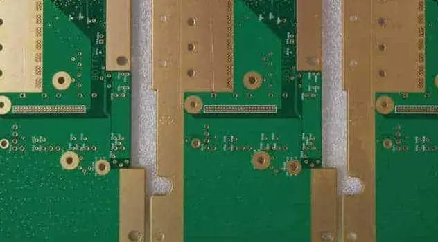
PCBs are in use to support and connect electrical parts in electronic gadgets. And are typically fabricated from copper, resin, and a substrate. The capability and strength of a PCB are directly related to its size and number of layers. Adding more layers to a PCB increases its functionality. This has significant advantages in the electronics industry.
Different types of Layered PCBs

1. Single-layer PCBs
Single-layer printed circuit boards (PCBs) are a form of circuit board that has only one thin coating of conductive material (often copper) on one part of the board. The other part serves as an attachment point for various electronic parts.
Therefore, electrical boundaries, fillers, connectors, components, wires, mounting holes, vias, and pads are all fabricated using a single-layered PCB substrate, conducting metal layer, silk screen, and protective soldering mask.
The electronics industry still relies heavily on single-layered PCBs despite the advent of more advanced technologies.
Pros of Single-SIDED BOARDS
- Cheap to produce
- Simpler and less error-prone to develop
- As there is only one layer. So, soldering, mounting, and electronic drilling components are simple.
- A good choice for minimalist layouts
- economical for mass-producing consumer electronics
- The best choice for fast, mass production.
Drawbacks of a Single-Layer PCB
Single-layer PCBs have the benefit of being simple and inexpensive to produce. But they also come with a few drawbacks that users should be aware of.
- There is a lack of room and pins for connectivity on printed circuit boards that need several components.
- Reduced velocity and productivity.
- As functionality increases, weight and size also increase, making the device less portable.
Coffee makers, calculators, radios, and even some types of cameras and cell phones use single-layered PCBs because of the space and weight savings they provide.
2. Multilayer PCBs
Stacks of double-sided circuit boards are used to create multilayered PCBs. It is common for these stacks to include three double-sided circuits. But they can include as many as necessary. However, warping or twisting may occur after soldering if the layer numbers used are odd.
Printed circuit boards with several layers get manufactured by laminating core materials and prepreg layers at high temperatures by melting the adhesives that keep the layers together and making sure that the conductors are thoroughly coated by resin. This procedure guarantees that no air gets captured in between layers. Epoxy glass, ceramic, and Teflon are a few of the many possible combinations of material used in multilayer PCB construction.
Multilayer printed circuit boards have a usage in a wide variety of electronic devices. Some examples include laptops, file servers, global positioning systems, heart monitoring systems, medical apparatus, handheld equipment, satellite systems, signal transmission, space probe technology, nuclear detection system, and cat scan system.
Benefits of a Multilayered OR DOUBLE SIDED PCBs

· Appropriate for complex projects
With the addition of more layers, multilayered boards may accommodate more circuits and connections. This allows the board to get used in devices that are more complicated. And, so require more components and circuits.
· Durability
More layers mean a thicker, more robust board. This will allow the board to survive rough treatment and maintain its integrity for longer.
· Connection
When using a single-layer PCB, many components would typically require multiple connection points. With this benefit, manufacturers can create compact and lightweight gadgets with minimal design requirements.
· Increased Capacity
Power-hungry gadgets can benefit from multilayer PCBs because of their increased density. This means more robust devices can function effectively.
Drawbacks of Multilayer Layer PCB
· Costly
To create a multilayer PCB, more resources, knowledge, and time are needed. Thereby, they are significantly more expensive than a standard single-layered board. The manufacturer is responsible for ensuring that the multilayered board will get used in a worthwhile project.
· Longer Lead Times
Multilayered boards take more time to design because of the complex needs of the layering phase.
Due to the complexity of the production process, the time required to complete it gets increased.
· Challenging to Repair
Repairing a malfunctioning PCB with multiple layers could be challenging. This is due to the fact that the problem’s origin may lie hidden within a layer that is not visible from the exterior. As the number of layers on the board increases, so makes it is difficulty to fix it.
Multilayer printed circuit boards are typically characterized as rigid PCBs. Because of the difficulty in fabricating flexible multilayered PCBs. The typical number of layers for a multilayer PCB is between four and eight. Cell Phones can have as many as twelve layers. Though that number largely depends on the complexity of the software in use. Also, companies prefer an even number of layers over odd ones when laminating. An odd-numbered layer might lead to an overly complex and problematic circuit. The high price tag is also something to think about.
However, a typical multilayered PCB consists of the layers listed below in the following stackings:
3. Two-Layered Printed Circuit Board
Both sides of the double-sided PCB are copper-plated, and an insulating layer lies in between. A double-sided printed circuit board is similar to a single-sided PCB. But features elements on both parts of the board. They are made by sandwiching a dielectric substance between two copper layers. And then connecting the two layers together. Systems where small packaging and high-speed are desirable benefits from the copper on both sides’ ability to convey various electrical signals.
The dielectric material in the middle prevents the electric signals from interfering with each other as they travel between the two copper layers. The most typical and cost-effective PCBs to produce are those with only two layers.
4. Four-Layered PCB
PCBs with four conducting layers are the four-layer PCBs. These layers include two inner layers, a bottom layer, and the top layer. The bottom and top layers are for elements and signal routing. At the same time, the inner layers comprise the core and are typically utilized as ground or power planes.
Soldering masks with uncovered pads provide mounting locations for through-hole parts and surface-mount gadgets. They are commonly applied to the outer layers. When the four layers get laminated together, they function as a single board, with connections made through holes.
Just to give you a brief idea, these layers are as follows:
The first layer is the base and is often constructed of copper. It’s there to keep everything else on the board fixed.
The power plane is the second layer. Its name comes from the fact that it is responsible for supplying the board’s various parts with a steady and pure supply of energy.
The third layer is the ground plane. It provides a common ground reference for all the circuitries.
The top layer is the fourth layer. It handles signal routing and component interconnections.
This is how a typical four-layer printed circuit board gets stacked. But, it can get changed to accommodate different designs or the layer carrying the most signals.
There is a wide variety of uses for four-layer PCBs since they are so much more flexible than two-layer PCBs. Strong signal quality and temperature control are further benefits of the extra layers. These are only some of the many reasons why they are preferable over two-layer PCBs.
5. Six-Layered PCB
A six-layer printed circuit board (PCB) consists of a four-layer board with two additional signal layers inserted between the planes. Four routing layers (two external and two internal) and two internal planes make up the basic six-layer PCB pile (one for power and the other for ground) by providing two inside planes for high-speed transmissions and two external layers for routing low-speed data. EMI is greatly amplified. An electronic gadget’s signaling can get disrupted by electromagnetic interference (EMI). It can come from either induction or radiation.
There are a variety of possible configurations for a six-layer PCB stack up, with the amount of ground, signal, and power layers depending on the intended function.
The bottom layer, prepreg, internal power plane, core, internal route layer, prepreg, internal route layer, core, internal ground plane, prepreg, and top layer; this is the basic six-layer PCB pile.
Even though this layout is typical, it may not work for your PCB design. You may need to switch around the layers or add more of one. However, placements should get made so as to maximize routing efficiency while minimizing crosstalk.
6. Eight-Layered PCB
A typical eight-layer PCB has four planes and signal layers. Among these are the signal, power, and ground layer. The power and ground planes isolate the various layers of signal and lessen interference between them. An eight-layer PCB’s stack-up provides superior routing, improved signal traces, and more productivity, all of which are especially important for highly integrated, small devices.
High current patterns, which are often quite large and have a lower impedance, are another advantage of 8-layer PCBs.
Furthermore, they offer high-speed signal transmission, improved EMC performance, and improved ground and power plane isolation.
Explanation of Layered PCBs
· Layer of Substrate
PCBs typically have a fiberglass layer of substrate, which provides the board with its rigidity. Excluding flexible circuits, which are constructible on flexible material like Kapton. This material will serve as the substrate for the vast majority of circuits. While other materials, like epoxies, can be used to create the layers of a substrate PCB, they cannot compare to the longevity that FR4 (which is present in fiberglass) offers.
· Copper Layer
The next step involves applying heat to the board and laminating a thin coating of copper foil to it. When we talk about multilayered PCBs, we’re describing the number of copper layers they have. Single-sided printed circuit boards (PCBs) only have one covering of conductive material, while both sides can be utilized to mount electronic parts. Alternatively, components and conducting copper can get mounted on both surfaces of a double-sided PCB rather than simply one. Traces on these double-sided circuit boards can get routed more closely together since they can jump between the bottom and top layers via interconnects. Many electronic devices can benefit from this, as the circuitry on opposite sides of the circuit board can get linked via the holes bored into them.
Your PCB’s copper layer thickness should reflect the amount of power it expects to handle. PCBs that are constantly subjected to high levels of power might have a thick layer of copper than those that aren’t.
· Soldermask Layer
The solder mask coating goes on after the layer of copper has been put. This is what provides the PCB with its distinctive green hue and serves to isolate the layer of copper from the other metals and components on the board. Since it aids the user in soldering to the precise places, this coating is also vital throughout the production process when the parts get connected to the board.
· Silkscreen Layer
Adding text, symbols, and numbers to the board’s silkscreen ensures that it is for the benefit of humans so that we may have a deeper understanding of the circuit and the purpose of various LEDs or pins.
Conclusion
Before the advent of multilayered PCBs, which offered maximized advantages for additional needs, Single-layered PCBs were utilized in most electrical equipment. However, as the globe has become more technically advanced. Multilayered PCBs have taken over the market. In spite of this, single-layered PCBs are still useful for low-tech gadgets. On the other hand, multilayer PCBs are common in high-tech gadgets.