What is the Standard PCB Panel Size?

PCB panelization

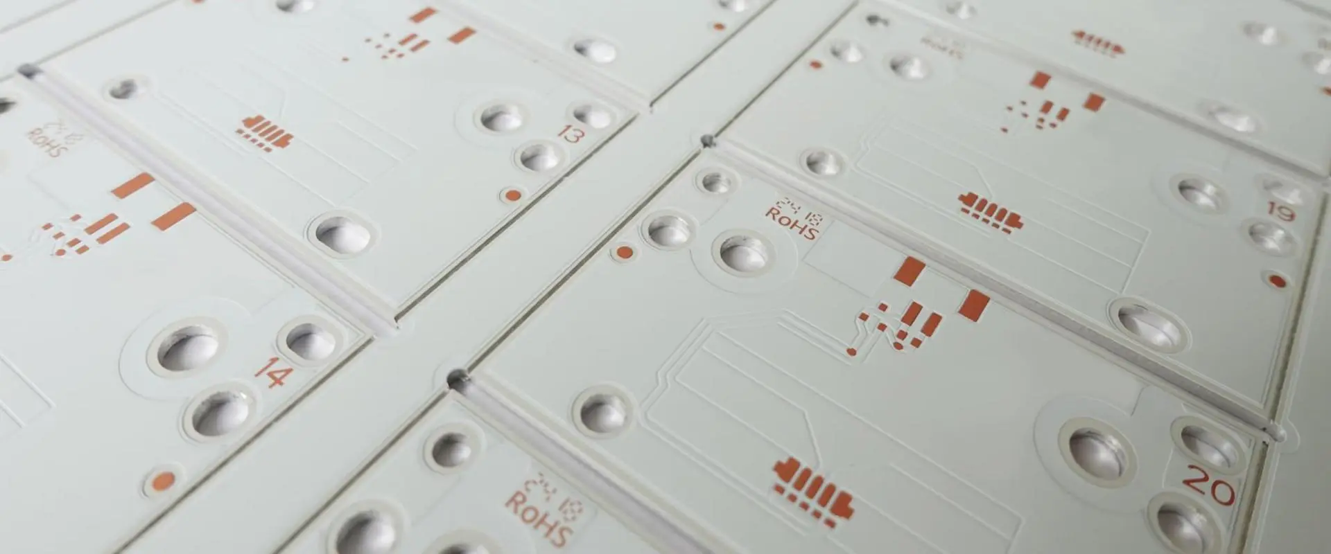
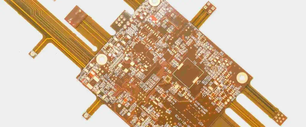
The size of a Printed Circuit Board (PCB)โ€™s panel can impact the outcome of the design. It is all a part of the broader panelization method. In this article, you will find out what the ideal size of a circuit board panel is.

What is PCB Panel?

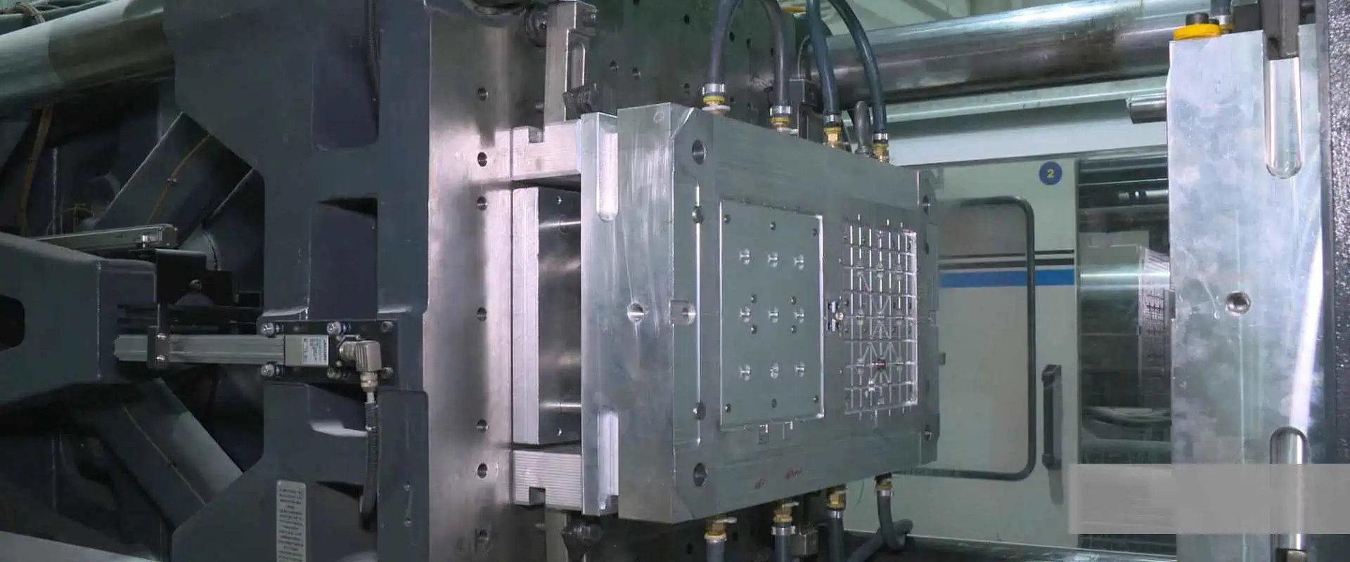
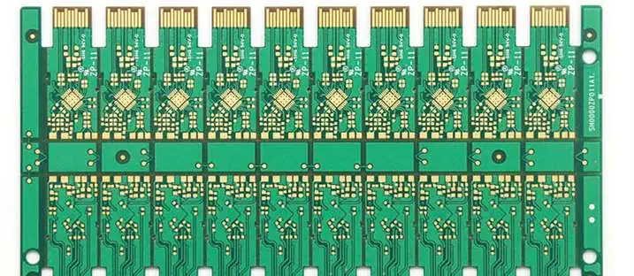
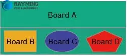
The panel refers to the platform where the circuit board is fixed for full production. In another perspective, it has to do with panelization โ€“ the process of fixing several circuit boards on the same panel.

How Important is PCB Panelization?

The panelization of a circuit board is important for these reasons:

  • It helps the circuit board designer to determine the number of panels that are required for the board.
  • With panelization, multiple circuit boards can be fixed to form a single array.
  • You can also use panelization to determine the amount of waste to be realized per panel.
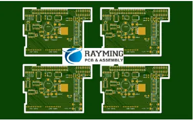
  • PCB panelization could aid in streamlining the production process, especially with the formation of a larger panel and the placement of individual, smaller circuit boards on the top.

Common PCB Panel Sizes

Combination Panelization

You will find an array of options when measuring the size of a circuit board panel. The common measurements include:

  • 18 by 24 inches
  • 18 by 12 inches
  • 9 by 12 inches and;
  • 9 by 24 inches

There is also a need to have a space between the boards on the panel. This is essential for automated routing and allowing for manual removal. The space given often differs by the PCB manufacturer โ€“ while some go with the standard 0.5-inch or ยฝ, others would prefer 1-inch.

Nevertheless, the 0.5-inch spacing is prioritized for the double-sided circuit boards. If it is a single-sided circuit board, then using the 1-inch clearance around the panel border is recommended.

The space between the boards and which is positioned near the panel border is not the only one given. You can also use a routing space of 0.1-inches, which would be given between individual circuit boards on the panel and not used for any other purpose.

Balancing the Space Constraints in PCBs

The spaces left in a circuit board might be limited or multiple, depending on the PCB panel size standard used. While the aforementioned are the common sizes, you can also make modifications if the panel is meant to occupy more boards.

Here are some of the important points to note:

1.    Take Cognizance of the Size from the Onset

By recognizing the size availabilities at the onset, you can determine if the panel has enough spaces to hold the circuit boards. Look over the horizontal length and width to see if these would provide enough surface area for matching the clearance requirements, the numbers of circuit board components, and the traces and connections.

2.    Be Selective with the Board Sizes

You also need to be choosy with the size of the panel. As a rule of thumb, do not use board sizes below 75 mil by 75 mil. This will give enough space to fit the components and make other modifications to the panel.

3.    Using the Panel Sizes is Recommended

Your Contract Manufacturer (CM) can also determine whatโ€™s best for the device, make the necessary variations and determining the best panel size to use.

However, sticking to any of the standard PCB panel sizes is ideal because it will help you maximize the yield (the number of circuit boards) placed on the panel. The manufacturer can also make additional changes that reflect on reducing the overall costs and producing a few extra boards per panel.

4.    PCB Dimensional Adjustment

Looking to get more circuit boards produced per panel? Besides relying on a manufacturer, you can also rotate the boards or make a slight modification to the boardโ€™s dimensions.

5.    Consider Combining Different Circuit Boards

It is also possible to place several circuit boards of different sizes, but with the same thickness, on a PCB panel.

There is also a possibility of placing a series of PCBs with different arrangements on the same panel.

With any of those two options, you can be sure of getting more circuit boards produced on the same platform, just by reordering the placements and using different PCB panel sizes.

What You Need to Know About a PCBโ€™s โ€œUsable Areaโ€

Order Panelization

A usable area in a PCB panel refers to the part or section where most of the panelization processes can be fully-implemented. Hence, any actions taken out of this space might result in a lower yield.

On this ground, the following facts are worth noting:

a.    Larger Process Area is Ideal

A large process area or more space is recommended, because it helps you to fit more boards into the panel. Besides, a larger process area is cost-effective, as it drastically reduces the efforts and numbers of boards to be produced with difficulties.

b.    Use Tabs on the Panel

There may be a need to use tabs on the circuit board panel. This is the case when the space is limited. With the tabs, you can have Through-Hole (THT) parts passing through.

This is highly-recommended when the client asks the Contract Manufacturer (CM) to deliver a complete panel.

Hence, by using tabs or holes for locating, the easy breakaway for the insertion of THT parts will be realized. This can as well, be extended beyond the usable area of the PCB panel.

Optimizing the Standard PCB Panel Size via Panelization Methods

Several panelization methods can be used to further optimize the numbers of circuit boards that can be fitted onto a panel. Find out more in the next paragraphs.

a.    V-Score

The V-scoring method of panelization has to do with the use of V-shaped grooves to differentiate the circuit boards. By using a machine to complete the breakout process, the depanelization process is simpler and reducing the thickness of the board is realized by using an angled blade.

b.    Solid Tab

The solid tab panelization method deals with the use of solid tabs to design arrays between the circuit boards. This process also boosts the overall strength of the boards.

A wide range of options can be explored for depanelization. Examples are:

  • Depaneling Router: this is not always used because of the dust and vibration it causes.
  • Laser-Cutting Machine and;
  • Hook-Shaped Blade: although this depanelization method is affordable, it is not efficient.

c.    Tab Routing

This is recommended as an option when the V-scoring panelization method doesnโ€™t work. Tab routing a PCB means pre-cutting the board at the array and using perforated tabs to hold it.

Out of those three options, the V-scoring panelization method is recommended for these reasons:

  • It reduces surface stress.
  • In addition to being affordable, the method is also easy to depanel.
  • It increases material utilization.
  • The V-scoring panelization method enables an easy removal of the circuit boards from a single panel. As such, spaces can be created for placing more boards, in place of the open space, initially designed for creating a route path.

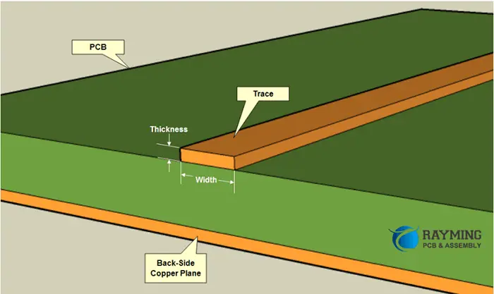
The Correlation between PCB Panel Size and Board Thickness

pcb panel & pcb panelization

The standard PCB panel size can, sometimes, not make do without the thickness. The standardization of the circuit boardโ€™s thickness can be dated back to the days of commercialized Integrated Circuits (ICs), but that is a story for another day.

Currently, there is a relationship or synergy between the size and thickness of a PCB. On one hand, using the right thickness and combining it with the ideal PCB panel size aids the realization of a perfect circuit board.

The question then is, โ€œwhat is the ideal PCB thickness?โ€ While there are ranges to this, the standard PCB thickness is 0.06-inch or 1.57mm. This is recognized as the standard, because it can fit into different applications and meet your needs.

However, this is not ruling out the possibility of โ€œstepping downโ€ to smaller options, especially if your applications require so. In that case, you can explore from any of the following:

  • 0.031-inch or 0.78mm: for smaller applications and;
  • 0.093-inch or 2.36mm: for larger applications.

The PCB thickness is important for these reasons:

  • It plays a crucial role in the upgrade of a circuit boardโ€™s core. For example, the 2.36mm or 0.093-inch or thickness can be used to extend a four-layered circuit board stackup, up to 6 layers.
  • If you are extending the four-layer stackup to 8 layers, you would need to use the PCB thickness of 3.18mm. In addition, you will add new core/prepreg layers to the original stackup.

Although the thickness is important and can help the PCB designer make an excellent design, it should be used with moderation. Here are some precautions to take:

  • The focus should not only be based on the circuit boardโ€™s thickness, but also on the standard panel sizes.
  • Use a thickness value of 0.063-inches for an average PCB.
  • Avoid using a prepreg dielectric layer thickness that is below 3 mil.

Conclusion

Using the ideal PCB standard panel size can save you the headaches of not placing more boards on a panel and optimizing the same for the best performance. As a general rule, the panel size and the PCB thickness should match for optimum performance.

What are the Materials and Components of Rapid Injection Molding?

rapid injection molding

Rapid injection molding, denoted as RIM can be described as a process of injection molding that is designed for manufacturing small batches or groups of plastic components with lead times that are much shorter.

Generally, this equipment utilized for rapid injection molding is similar to that utilized for normal injection molding rather than the rapid injection molding molds which are designed for the fast turnaround rather than for production durability for long series.

The gain in the idea to manufacturing lead time is seen mainly from utilizing mold materials such as aluminum that can be machined easier and less expensive compared to the standard materials for injection molds. These molds will lack the needed durability for long production runs; however they work well for runs that are smaller, with a minimum of 500 parts.

In this article, we will be describing the process involved in rapid molding. We will explain the way it works, and we will discuss the type of equipment utilized. Also, we will provide you with some tips on how to select the best part materials.

What Does Rapid Injection Molding Mean?

Rapid injection molding utilizes standard injection molding techniques and equipment. However, they achieve this within a very short lead time and at a lesser cost. The short lead time is great for the custom prototypes as well as producing the limited volume runs to straighten out all potential issues elating to the design before going into full-scale rapid molding.

The speed is majorly as a result of using less expensive molds as well as materials that are easy to machine such as aluminum which could be produced within few weeks. Also, rapid injection molding should not be mixed up with the reaction injection.

Where Can Rapid Injection Molding be Used?

 injection molding
injection molding

The process of rapid injection molding is mainly utilized for research, rapid injection molding prototyping as well as developmental applications, which donโ€™t need millions, thousands, or as few as hundreds of parts. Rapid injection mold is well suited to production runs having volumes of a minimum of 500. With this, engineers will be able to test all their designs even with less capital investment rather than committing to the expensive, lengthy lead-time tolling required for the series production of high volume.

Usually, producing injection molds can cost very much in part due to the fact that they have to be manufactured from very wear-resistant materials. This is to make sure that they will be able to withstand the stress involved in production use for long use.

This is why rapid injection molding is usually utilized in bridging the gap formed between the initial design as well as the full-scale production. This is a less expensive option for testing the new materials, products, as well as design tools. Also, RIM may be utilized in managing the sharp increases in the volume of product demand.

How Rapid Injection Molding Works

The parts for rapid injection molding have to be designed using DFM principles. RIM mold are specifically created cheap and quickly manufactured making use of off-the-shelf and standard materials. Also, aluminum molds are utilized because they can be machines quickly and easily, but wonโ€™t be able to deal with high-volume manufacturing.

Immediately the manufacturing of the RIM mold is done, these two halves (cavity and core) may be mounted n the moving and stationary plates of thee normal setup of the injection molding machines. This is due to the fact that the remaining process of molding is similar or both the standard and RIM injection molding. The moldโ€™s halves are brought closely together and then held tightly in place with the use of hydraulic rams.

More Information on How Rapid Injection Molding Works

In order to make the part making use of the rapid injection molding process, raw materials used typically thermoset and thermoplastics silicones) is fed in a screw, which is housed inside a cylinder referred to as a barrel.

 Combining the heat offered by the external heaters, which are mounted on a barrel, which shear producing the heat between plastic pellets as well as the screwโ€™s action inside the barrel, helps in melting the plastic pellet. Immediately enough plastic is melted, this screw will push the plastic in the mold via a nozzle, as well as a valve that stops the receding of pressure back inside the screw.

Furthermore, high-pressure plastic will then fill the mold, and then hydraulic rams make sure that the plastic doesnโ€™t ooze out between its old halves.

After some seconds, this plastic will solidify causing the mold to open. This part will then be ejected making use of ejector pins, and screw retracts, and then the process will repeat again. You must note that the process of rapid injection molding will not produce any individual parts faster compared to the standard injection types.

Places Where Rapid Injection Molding Equipment are Made

Rapid injection molding equipment is manufactured by manufacturers of injection molding machines. These manufacturers are typically located in the United States, Europe, and China.

Take note that the major difference with respect to equipment between the standard and rapid injection molding types has to do with mold. Molds are usually manufactured with the use of the injection molding tool maker.

Components of the Rapid Injection Molding Press

Rapid injection molding press works with some components. The major components are parts utilized in the standard molding press.

Hopper

This is where you find the resin thermoplastic pellets placed for proper dispensing. This hopper is usually fed from a silo or bulk bags, which depends on the needed volume of production as well as the part size. The hopper offers a continual material supply onto the screw.

For some cases, this also aids in preheating the resin ensuring the rapid melting in the barrel and screw. With this, the per-part manufacturing cycle time is reduced. Also, the hopper might have some level sensors. This is to warn the operator that the material needs to be topped up inside the hopper.

Screw

This reciprocating screw comes with many functions. The first is that, it meters as well as transports the right material amount out of the hopper and in the mold. During the raw material transport, it rotates, which forces the pellets in the ever-decreasing volume that is created with the help of the screw shaft which is experiencing an increase in diameter. It creates much heat for melting the pellets through the shear force that the plastic pellets create shearing against the barrel and screw.

Also, there is a screw which mixes the material in order to create a melt that is more homogeneous and for some cases, makes sure that the additives are evenly mixed. Once the melting of enough materials has been done, this screw then rams forward and the one-way valve present on the screwโ€™s end keeps the material from moving back downwards the screw. Rather it is forced in the mold. After, this screw will then retract, them the process will be repeated.

Barrel

This houses the screw and it helps to guide the passage of the raw materials in the mold. Typically, this barrel will have heated elements that are wrapped round it so as to help melt the pellet. This screw will force the plastic pellet against its barrel. This leads to increased friction which then melts this plastic. You can find injection nozzles at the barrelโ€™s end.

Heaters

Barrels have some electrical heaters that are wrapped round it. This helps in heating the plastic pellet up. Note that the heating elements rent the main heat source for the melting of the plastic. Also, the screwโ€™s induced pressure forces these pellets against the barrelโ€™s inner part. This creates shear heating which also helps in melting the plastic.

Materials

Materials utilized in the process of rapid injection molding are referred to as thermoplastics. The materials could either be a specialty or a commodity. This is dependent on the end-use desired.

Nozzle

Nozzles help in directing injected plastic in the mold. Its diameter may fall between 2.5 and 10 mm. This depends on the injection molding machineโ€™s capacity. This nozzle is directly screwed to the barrel. Also, Nozzles might have filters for preventing any unwanted particles from gaining entrance into the mold. Two filter styles exist: the gap filters and the screen pack filters.

The screen pack filters arenโ€™t popular. This is because they impede flow via the nozzle, thereby creating a loss in pressure whereas the gap filters offer a greater filter area and doesnโ€™t impede flow too much. Also, nozzles could have the mixing function which helps in creating the homogenous melt as well as aid in the dispersion of additives such as colorants evenly all through the melt.

Mold

Typically, the mold is made from two main parts: the cavity and the core. These parts and sections of the mold are mounted to plates referred to as a platen. One of the moldโ€™s half is held in a stationary way while the second half will be pressed against it using the hydraulic arm.

The ram will apply proper pressure to make sure the plastic doesnโ€™t exit that mold at a partying line. Often molds have some cooling channels that are machined in them that allows for the heat transfer fluid to get rid of heat out of the mold.

The cooling channels aid the part to solidify faster as well as reduce the cycle time overall. Immediately that part solidifies them the molds will open and some ejector pins would push that part out of the mold. This mold would close and then the cycle will repeat.

Rapid injection molding molds are created utilizing easier to machine and less expensive materials. They are also designed to last just for some hundred parts. Also, another method that can be used reducing cost as well as increase the speed of production is to utilize mater unit dies that permits modular mode, which ensures quick design implementation of the changes in deign without manufacturing the whole mold right from the scratch.

Part

Part has to do with the eventual result from the process of injection molding. Injection molded parts has to be designed in line with the injection molding DFM principles. This is to achieve parts with high quality. These rules will help in determining the most appropriate wall thickness, hole sizes, here the ribs should be reinforced, etc.

Wall Thickness of the Rapid Injection Molded Part

Rapid Injection Mold

The rapid injection molding partโ€™s wall thickness usually falls within 1.5 to 2.5 mm. Moreover, the thickness will also depend on that material used as the different materials usually have several ranges for the best wall thickness.

No difference is found between wall thicknesses that are common with the standard injection molding as well as what can be possible with rapid injection molding.

Choosing the Best Possible Materials for Your Rapid Injection Molding

Selecting the most appropriate material for rapid injection molding is dependent on the desired use of that product. Rapid injection molding is utilized for pilot, prototype, as well as short-run volumes. This bridges the gap present between the full-scale production and design. One major benefit of the RIM is, many materials could be tested in order to know which of them is optimal. Some major considerations whenever you are deciding on the most appropriate material are UV resistance, mechanical strength, cost, thermal resistance, and electrical properties.

You can enhance these properties by including additives like carbon or glass filters. Also, you must note that these fibers are highly abrasive and could reduce the moldโ€™s overall life which holds true for the aluminum molds.

Conclusion

In this article, we have explained what rapid injection molding is, as well as discussed the several parts if the rapid injection molding press. To know more on rapid molding, please reach out to any of our representatives. Our Company offers different manufacturing capabilities, which includes injection molding as well as other value services to meet all your manufacturing and rapid injection molding prototyping needs.

What is Substrate in a PCB?

aluminum substrate pcb

Every building needs a โ€œfoundationโ€ or a โ€œplatformโ€ upon which the structure will stand. The absence of such makes it impossible for such a building to stand โ€œthe test of time,โ€ as it is susceptible to collapsing after some time. The same applies to the production of Printed Circuit Boards (PCBs). There is a need to have a substrate in the PCB and that is what we will discuss in this article.

Why a Substrate is the โ€œFoundationโ€ of a PCB

A Printed Circuit Board (PCB) is merely a โ€œflat or bare board,โ€ which wouldnโ€™t stand on its own and perform excellently, except if it has some properties. This is why the board is โ€œequippedโ€ with a non-conductive substrate material that has both conductive pathways and electronic components attached to it.

The substrate is aptly described as the โ€œfoundationโ€ or โ€œbase materialโ€ of the circuit board, because it is both a non-conductive material and a dielectric composite structure made from epoxy resin and either paper or glass fabric.

As such, the substrate provides the foundation or platform that โ€œholdsโ€ the electronic components and traces in place. Therefore, you can leverage the substrate used in PCB to securely hold the foundational parts and electronic components on the circuit board.

The Types of PCB Substrates

You will find different kinds of base materials used in the production of Printed Circuit Boards (PCBs). Of course, the properties and or functionalities of these materials differ.

Here is a list of some of the popular/common PCB substrate materials:

1.    FR-4

This is not just the most popular PCB substrate material, but also the one that offers the best performance.

The Flame-Retardant 4 (FR-4) circuit board substrate is commonly made out of a woven glass reinforced by epoxy resin. It is also said to be fire-resistant, because of the properties of the epoxy resin used:

  • The epoxy resin is always Flame-Retardant Level 4.
  • The epoxy resin doesnโ€™t absorb moisture and;
  • It is water-resistant.

a.    Features of FR-4 PCB Substrates

Besides offering the best performance and being used in a vast majority of circuit boards, the FR-4 substrate has these characteristics:

  • High electrical insulation, hence, the fireproof.
  • Lightweight design
  • Higher moisture resistance
  • Lower cost
  • Excellent performance
  • Higher electric strength

b.    Applications

The use cases of the FR-4 substrate are often prioritized for the low-speed digital circuits. You can also use this substrate with the circuit boards that have a complex structure, as well as the PCBs requiring several layers.

It is true that this substrate can be used for a wide range of circuit boards and consumer electronics, it does have a higher dielectric loss. This is the reason why FR-4 substrates are not always ideal for either the high-frequency or high-speed applications.

c.     Different Variants

You will find different variations and or versions of the FR-4 PCB substrates. Of course, they differ in terms of the properties and performances.

These are some of the variants:

  • Halogen-Free FR-4: this variant contains less halogens and these are one of the fireproof elements.
  • Standard FR-4 Substrate: this type of substrate is considered to be the โ€œstandardโ€ or the format for others, because of the economic undertone. It also has a higher heat resistance, of up to 150-degree Celsius.
  • High Tg FR-4 Substrate: this type of PCB substrate is prioritized for the higher temperatures. It is noted for the higher value of Glass Transition Temperature (Tg) โ€“ an attribute that supports the substrateโ€™s clocking of higher temperatures, of up to 1180หšC.

2.    Teflon

Teflon is a brand name for Polytetrafluoroethylene (PTFE), which has a Glass Transition Temperature (Tg) of 160. It is a type of plastic that doesnโ€™t offer resistance, which is why it is always used with high-frequency and high-speed signals.

PTFE is highly-recommended for the high-frequency, microwave and high-power PCBs.

Properties

The features include:

  • Excellent high-frequency properties that make it ideal for electronic devices that handle higher signals, ranging from a few hundred MHZs to tens of GHZs.
  • The flame-resistance, flexible and lightweight design makes it ideal for different kinds applications.
  • The low dissipation and excellent temperature stability makes it usable in aerospace telemetry, cruise control, antennas and power amplifiers.

3.    FR-2

This is the Flame-Retardant Level 2 (FR-2) substrate. Although it has fireproof properties, it offers a lower performance, when compared to the FR-4 substrate.

It is made of a phenolic material and is commonly used in economical and low-cost consumer electronics, an example being low-cost transistor radios.

4.    Flexible Substrates

These substrates are not only flexible, but also offering the best performances, without compromising the circuit boardโ€™s electrical continuity.

The major attributes are wrapping, bendability and folding โ€“ making it easier to optimize the boards for different applications. Circuit board designers also leverage this to fit the substrate into the tiniest of spaces in the PCB.

5.    CEM-1

This is the type of substrate used in producing the single-sided circuit boards. The CEM-1 substrate has a Dielectric Constant (Dk) of up to 5.4 and is recommended for use with the high-density PCB.

If you cannot afford the FR-4 substrate, then using the Composite Epoxy Material 1 (CEM-1) is an ideal alternative.

6.    Polyimide

flexible printed circuit

This type of PCB substrate is higher Tg of up to 250-degree Celsius, which makes it ideal for use with the high-temperature applications.

Unlike the CEM-1, which is a cost-effective variant to the FR-4 substrate; the Polyimide substrate is costlier than the FR-4.

The attributes include:

  • Solid conductive properties
  • Flexible use to develop both Rigid-Flex and Flexible PCBs.
  • Good temperature range and;
  • Higher chemical resistance.

7.    Rigid PCB Substrates

These are the opposites of the flexible substrates. The rigid PCB substrates are rigid or โ€œimmobile,โ€ hence, they cannot be relied on to offer a similar bendability and or folding, as the flexible PCB substrates offer.

Conclusion

The different PCB substrate types offer you a plethora of options to choose from. Rest assured that by using the FR-4 substrate, you will be able to make different kinds of circuit boards.

If you are not cool with any of the options on this list, you can always contact your substrate PCB manufacturer for recommendations.

What is a Copper Trace PCB and Why Is It Important?

copper trace pcb

When talking of PCBs, trace typically deals with a boardโ€™s network of fuses, copper, wiring, and insulation. Whenever any electronic equipment malfunctions, then the PCB tracing will most likely be inconsistent. Also, engineers in the PCB field always make use of this phrase โ€œtrace resistanceโ€ very frequently.

In addition, the trace resistance deals with a boardโ€™s components which serve as a barrier to free electricity flow.

What Does Copper Trace PCB Mean?

Every PCB is dependent on the trace. This is similar to the pcb trace current, which is for effective operation. Also, any errors in calculating and detecting the trace would require more effort and time utilized during fitting. In addition, this can make devices or any gadget to have errors, which could be bad for the user.

During the repair or assembling o a printed circuit board, you should be very familiar with the components contained in it coupled with the functions and formulas that will suit your requirements and needs.

Why You Should Use the Copper Trace PCB

Diagrammatic Representation of Copper Trace

One great quality of copper is its great conductivity. This makes sure of the minimal loss of energy during the transmission. Also, manufacturers have what it takes to save much copper when it doesnโ€™t use too much. Standard PCB layouts could use just an ounce of metal to cover one square meter of the substrate with a copper layer with thickness 35 micrometers thick. Also, you can easily get access to copper and it is extremely affordable.

Many capabilities as well as features of PCB s are possible. This is happening due to electricity. These boardsโ€™ circuits are just conduits for the proper electric current transport between two different points. This is why their performance is very important. The material of choice is copper due to its high conductivity, although a dozen other materials can transfer electricity as well.

Due to the fact that just one electron is contained in its valence shell or free electron, this copper is known to have a great electron mobility, thereby making it a great conductor. In addition, these electrons feature low barriers to crossing between two atoms. Since the electrons form the basically-charged particles, the free electrons are those responsible for the transmission of electricity. This copper helps in preventing the loss of energy during the impulse transmission.

With all these reasons stated above, the most appropriate material for your PCB traces or traces in PCB is copper.

What is Copper Trace PCB Resistance?

One important aspect you should look into during the PCB design is the tracesโ€™ resistance. Resistance is one out of the many qualities that is shared by all the materials in the cosmos. Usually, PCBs make use of copper; however copper comes in different forms, with each form coming with its own drawbacks and benefits. The designing as well as the execution of problems can arise out of the resistance of the PCB tracing. Circuits that are more complicated would definitely experience more problems.

Copper Trace PCB Resistance Calculation

When you apply ohmโ€™s law to a known data, then you can easily determine the tracing resistance. The estimator for the PCB tracing resistance is an in-built feature of the majority of design applications and suite frameworks, which can aid the prediction of the resistance of the copper trace on the board.

Furthermore, this calculator works with an algorithm that is universally applicable in determining the challenge level, thereby guaranteeing that this result would always be the same, regardless of where it is utilized.

The height, width, and length stand in for the traceโ€™s actual dimensions. This word PCB stands for the resistivity of the materials, whereas this symbol stands for the temperature coefficient of copper. Moreover, these calculationsโ€™ results are just approximations. The eventual cost of the material would alter by a minimal amount after the manufacture.

Resistance Calculator for the Copper Trace PCB

Printed circuit boards all make use of some standard formulas. All the tracking resistance would be nowhere to be found if this was an incorrect formula. Not understanding the way the PCB tracing resistance is computed is a well-known error usually made.

Using the Equation for the Copper Trace PCB Resistance

This phenomenon could happen in pcb trace current sensing systems which rely on resistance. This system would read a resistance of 1100 ohms rather than the standard 1000 ohms when one ohm sensing resistor is utilized with a trace of 0.025 mm.

This disparity is a huge one, and it could cause a drop in the currencyโ€™s value more than required or even needed. Also, manipulating the PCB trace thickness and width without working with some complex math is possible. Rather than calculate the PCB trace width, you may need to consider the alternatives.

If you wish to know the circuitsโ€™ properly associated with them, you can handle the first just by observing what the width is as well as raise or decrease it. This would accomplish different things. The first being that it would help in expanding the area of copper, offering additional wiggle room so as to try different resistance values out. Secondly, it would reduce the resistance of copper on the board. In addition, it would give more room for the testing to be able to establish the right trace width.

Why You Should Calculate the Copper Trace PCB Thickness

Simple procedures or calculations might not detect trace resistance accurately. Also, calculating the PCB trace might not be accurate or enough. Moreover, with an accurate calculation of the copper trace PCB thickness as well as the trace, is necessary to ensure the PCB tracesโ€™ proper activation. Any given resistance of the PCB trace could be reduced through the calculation as well as increasing the traceโ€™s width considerably.

Conclusion

Printed circuit boards are known to form the base and skeleton of many electronic devices and gadgets. When planning your printed circuit board, these are the things you must put in place. Every PCB is dependent on the trace. This is similar to the pcb trace current, which is for effective operation. Also, any errors in calculating and detecting the trace would require more effort and time utilized during fitting.

How You Can Use RF Signal Detectors to Protect Your Security

RF Hardware Engineer

Radio frequency signals or RF signal float through humans day to day activities. This allows us to learn, share, as well as communicate using devices such as phones, which are highly relied upon. Moreover, as technology keeps becoming prevalent and important in our daily lives, there are concerns regarding security and privacy. Although these waves could be important, they could also be used as a weapon for spying ion companies and different individuals.

In order to fight this issue, RF signal detectors, which are usually referred to as RF finders, could serve as a countermeasure technique for protecting very important information and assets. This could be in a home or large and secure facilities such as SCIFs.

What Does an RF Signal Detector Mean?

RF detectors can be described as electronic devices that are designed specifically for detecting RF signals like GPS trackers and other hidden devices for audio recording in vehicles, homes, as well as other spaces. Many people utilize them for their personal uses. These include AirBnB and finding spyware utilized in hotels. Also, they are used by government agencies, law enforcement agencies, as well as private companies for preventing the leakage of information from unwanted devices.

In the wireless world of today, the RF signal spectrum has started exploding when it comes to complexity. This poses new malicious threat levels to our national security. Some national laboratories are developing solutions for defense against any RF-enabled cyber attacks and espionage on governmentโ€™s critical infrastructure, facilities, telecommunications systems, aviation, as well as other important RF-enable environments.

Furthermore, the blending of multidisciplinary expertise in radio frequency, data science, computing, and cybersecurity โ€“ with the major strengths in machine learning and artificial intelligence, different engineers and scientists are creating novel capabilities which will increase the ability to properly understand, control, as well as protect our RF signal environments.

What is Real-time detection of RF Signals?

RF signal interference could threaten different wireless technologies that are commonly used on which so many areas of national security are dependent on like Wi-Fi, bluetooth, mobile radio, as well as GPS (Global Positioning System).

Furthermore, protecting the RF environments of our nation requires a better technical surveillance as well as countermeasure tools for different real-time analysis as well as response of the radio frequencies as well as other signals that are suspicious.

Some companyโ€™s researchers are working with some government sponsors to develop in-place and next-generation RF monitoring systems to help offer better protection for the government facilities against any RF-enable threats.

When you bring together any sophisticated logarithms for machine learning and high-performance sensors, the monitoring technology could detect as well as assess any signal anomalies around and in secure environments very quickly. This will enable more effective as well as faster responses to any RF signal interference.

Detecting RF Signals, Direction Finding, and Spectrum Analysis Equipment

Recently, radio frequency jammers have now become very accessible for public use. While the majority of RF jamming is intended simply to offer additional privacy, the first responder operations have been targeted specifically by the interference and jamming attacks.

The way a radio interference function works is that it targets receivers. The RF jammer would transmit signals on one frequency just like the signal desired. Although radio communications might be a very obvious target of the RF jammers, the sources of this interference could as well disrupt the other devices’ operations which communicate in a wireless manner. This can be seen in using the GPS (Global Positioning System) jammer by truck drivers so as to prevent the payment of highway tolls, as well as avoid an employer tracking him or her.

Alternatively, RF jammers targeting the first responder operations can be described as interference sources that prevent control centers from receiving any video uploaded by the traffic cameras.

Applications

RF jamming as well as interference could disrupt any first responder communications when emergency response situations and operations arise. Devices for detecting RF signals could be useful in identifying RF interference which may impact communications. Devices for spectrum analysis could also prove useful in identifying any interference-free frequencies should responders make use of channel switching as one of the tactics or RF jamming mitigation. The RF direction finders may help in finding RF jamming devices. Once you locate the source of interference, responders may apply direct tactics for mitigation to be able to overcome RF jamming impacts.

How Does an RF Signal Detector Work?

Different ways exist in which detectors can locate RF Signals. This depends on the detector type in use and the purpose it is intended for. The basics of the way RF signal detector works is, it captures the RF signal, analyzes it, as well as interprets the signals. Moreover, there are other sophisticated ways. These include:

Detection of Field strength

There are RF signal finders that have the ability of measuring an RF fieldโ€™s strength in a p[particular area. This is possible by making use of a sensor in detecting these RF signals. Immediately it is detected, they are turned into electrical signals that are amplified by the detector and then help in determining the wavesโ€™ strength.

Detection of Frequency

The RF devices that are most common are those having the ability and capability to identify RF signalsโ€™ frequencies though scanning as well as finding the accuracy. Immediately there is a frequency, this value is compared with others and then the range can be identified.

Detecting RF interference

A good number of RF signal detectors will find some unwanted or RF interference signals. These could disrupt the signals as well as communication. These RF detectors help in monitoring RF spectrums for any unexpected signals, which then notifies you whenever they discover one.

How to Choose the Right RF Detectors for Security

Selecting the appropriate RF detectors for security measures is dependent on the purpose and budget. For professional settings like those used in corporate buildings or in secured rooms, you would have to choose RF signal detectors that can detect different signal types like one that makes use of RF interference detection.

Also, for those seeking RF detectors for individual or personal use, portable detectors are many and small and you can get them online to serve simple purposes. Also, some RF signal detector applications are available which can give you a head start.

Tips to Work with when Choosing a Device for Detecting RF Signals

When searching for the best device for detecting RF signals, take note of these tips.

Detection range: Do you wish to secure an entire building or small space? Some come with a limited range; others could cover much larger spaces.

Range of frequency: most of the time, users desire one having a wide frequency range. This ensures that it covers a wide and broad spectrum. Moreover, this might be determined through the budget coupled with the area type that the frequencies need to be detected in.

Strength of the signal: It is preferable to use detectors having an adjustable sensitivity. The device can be fine-tuned to detect any stronger or weaker signals and assist you with detecting the RF signal through the showing of the signalโ€™s strength.

Alert Mechanism: Take a look at the way the device notifies you that a signal exists in that area. There are models that make use of lights or beeps while others usually vibrate. Although beeps might sound great initially, if you will be utilizing it to discover signals in a covert way, then it is advisable to work with silent light flashes.

Additional Features: Though a very significant aspect of RV detectors are signal detection, there are different models which come with more features in order to assist you with locating signals with cameras and signalsโ€™ log data.

Regulations: While our government and military can make use of sophisticated RF detectors to sole security measures, the usual RF signal detectors might come with laws and regulations on them. Therefore, before you buy one, ensure that your country or state permits the utilization of detectors. Also, if they permit it, be sure of the type to be used.

What is the Significance of RF Signal Detectors for Privacy?

The significance of RF signal detectors cannot be overemphasized. They are very important in different electronic countermeasures through offering assistance to the identification of possible threats from hidden cameras, listening devices, as well as other surveillance equipment that are wireless in nature.

Also, they have the ability to pick concealed and small devices that could be easily utilized for spying on institutions and individuals. When these signals are detected, security personnel and individuals will be able to take the right steps in protecting any sensitive area from any monitoring that is not authorized.

The utilization of RF signal detectors is also necessary for the prevention of information leaks or cyber attacks in any secured area. Furthermore, any wireless information could transmit data easily as well as gain access into the networks.

However, with the utilization of RF detectors, security personnel would be able to identify as well as locate unknown wireless devices which might be making efforts to content as well as compromise a particular network. Working with the appropriate device, the RF signal detector could play an important role in the protection of valuable data as well as prevent all cyber threats.

Furthermore, they are important tools for countering wrong and illegal surveillance using proactive approaches. By utilizing RF detectors, individuals and organizations have what it takes to enhance their countermeasure electronic techniques as well as aid in the maintenance of their privacy as well as other important information.

What are the Pros and Cons of RF Signals?

RFT Testing

Just the way RF signals has some benefits, it also has some drawbacks. Let us consider both

Pros of RF Signals

  • Their range is relatively long; it could take about 20 miles whenever there is a possible line of sight
  • It operates great in foggy and haze conditions, asides from heavy rain that results in poor performance
  • Operation is license-free and only for the 802.11 based systems

Cons of RF Signals

  • The throughput is lower and about the Mbps range
  • Great potential for radio frequency interference e from different RF-based external systems
  • Security is limited, which is due to the radio propagation beyond facilities

The benefits above utilize RF signals for many wireless applications. Majority of wireless networks like bluetooth and 802.11 specify the utilization of the RF signals.

Impairments of the RF Signal

The RF signal usually comes in contact with impairments like multipath propagation and interference. It has an impact on the communications between the receiver and the sender. This usually causes lower performance, leading to many unhappy consumers.

Interference

This occurs whenever there are two signals at a receiving station. This assumes they have one phase and frequency. For situations like this, the wireless NIC receiver encounters errors during the decoding of the informationโ€™s meaning being sent.

FCC regulates using the majority of frequency bands as well as modulation types. This is to prevent the occurrence of signal interference occurring between the systems.

Multipath

This happens whenever some areas of the RF signals take on different paths during the propagation from a particular source. A part of the signal may go into the destination directly, while the other part may bounce into the ceiling from the desk. From here, it reaches the destination. Due to this, some signal encounters lead to delay and then travel longer paths before reaching the receiver.

Conclusion

In summary, the significance of RF signals cannot be overemphasized. RF detectors can be described as electronic devices that are designed specifically for detecting RF signals like GPS trackers and other hidden devices for audio recording in vehicles, homes, as well as other spaces. Radio frequency signals or RF signal float through humans day to day activities. This allows us to learn, share, as well as communicate using devices such as phones, which are highly relied upon.

What is the Importance of Optical PCB?

Optical PCB

The interconnection required to boosting the performance of Internet switches is directly proportional to the final outcome of data aggregation. As the next-generation Internet switches emerge, we need a reliable interconnection to make them work. That is what you will get by using optical PCB.

In this article, we define what an optical circuit board is, the relevance in the market and some of the benefits.

What is an Optical Printed Circuit Board?

It is a type of circuit board used to produce dedicated interconnects, required for the connection of optical interconnects.

Optical Interconnects on a PCB?

You may be wondering why these interconnections are brought to the PCB-level. Given the ever-increasing use cases and or applications of Printed Circuit Boards (PCBs), it is not entirely surprising that optical interconnections are made here.

At the core is the need to leverage fiber optics, as a means to an โ€œendโ€ โ€“ towards forging an integration of optical interconnects onto Printed Circuit Boards (PCBs).

This is a step away from the conventional use of chip-to-chip interconnects, which, though have been in use for some decades, is now giving way to newer technologies.

Today, we can now commercialize optical interconnects, on the basis of Photonic Integrated Circuits (PICs).

Although todayโ€™s optical PCB is still based on a construction out of COTS components, we are optimistic of what the future holds.

Market Opportunity: Why Optical PCBs Became Popular

Automated-Optical-Inspection

The primary goal for producing optical circuits is to streamline the speed of processing data rates.

Other reasons include:

1.    The Need to Prevent Signal Loss Issues

The current Internet switches are not fully-equipped to handle the data rates. With the expectations of higher data rates from the next-generation Internet switches and high-end computers, it has become imperative to step-up on the performance of these switches.

However, the current switches are processing data packets (rates) in Gigabytes per second (Gbit/s). This is lower than the anticipated Terabytes per second (Tbit/s) data rates of next-generation Internet switches.

If the current switches and interconnection technologies are relied for this, one can be sure of signal loss, in the process of transmitting data rates.

2.    The Wire Geometry Consideration

This is another important consideration. The geometry of the wire makes it nearly impossible to leverage the existing electrical interconnection technology. For example, we currently have more of copper wiring that inhibits data transmission rates in the following ways:

  • The inverse proportion of the wireโ€™s length to the cross-sectional area, and the proportion of the resistance to the wireโ€™s length.
  • The wire is usually thinner, and this further reduces the data transmission rates.

3.    Limitations in Scaling

There is currently a challenge in scaling or extending the performances of electrical/optical interconnects. This is because of several factors, such as:

  • Reflection
  • Signal loss
  • Crosstalk
  • Space constraints that donโ€™t allow for thicker wire usage
  • An increase in noise and power consumption, due to the use of a harder connection to reduce conversion time.
  • An increase in power consumption and operational costs for scaling current interconnects, up to 100 Gb/s.

How Optical Interconnects are Integrated into PCBs

Optical interconnects are currently constructed from the COTS components, but there are indications that, in the future, we will have these interconnects directly printed on the circuitsโ€™ substrates.

It is also worth noting that the integration of optical waveguides in the PCBs also aid the integration of optical interconnects. With the potentials, these would greatly improve the overall performances of the onboard interconnects.

The Advantages of Optical PCB

Besides reducing the link length for the high-speed electrical signals, the integration of optical interconnects into PCBs also offer these benefits:

a.    Independent Propagation of Signals

Signal loss and integrity problems are the common challenges with conventional electrical interconnection technology. This is now been tackled with the fusion of optical interconnects into PCBs.

The optical signals can now make independent propagations, devoid of the restrictions in space. This is also enhanced by the use of an imaging processing technology that delivers good dimensional integrity of the waveguide layer.

b.    Improved Speed and Overall Performance

The overall performance of the optical circuit board is assured, because of these reasons:

  • The optical interconnectionโ€™s speed is separated from the interconnection channel.
  • A photo-imaginable waveguide material is used to help meet the processing and functional requirements.

c.    Improved Reliability

With the optical PCB technology, one can be certain of deriving improved reliability of the signals, courtesy of these reasons:

  • Optical signals can propagate in three-dimensional (3D) free space.
  • There is a considerable increase in the data transmission rate.

d.    Balancing Performance and Cost

It is now possible to have both an improved performance at affordable costs, with the new optical PCB framework.

In addition to reducing the physical size of the electrical connection, it also aids the reduction of power consumed, while cutting down on the cost of the material used.

Typical Applications for Optical PCB

Cavity PCB board
Cavity PCB board

With the inputs of the optical circuit boards, we can now see that the use cases for these boards are further expanding. Now, you can use these boards to enhance the different applications and communications.

The following are some examples of the typical applications:

  • Opto-micromachine
  • Telecommunications and;
  • Photonic interconnection

Besides the above, optical circuit boards have also been used in other places. Most importantly, the photonics and optical interconnects jointly enable the usage in advanced applications, such as:

  • Future Telecommunication Networks: these are used to reduce the numbers of electronic components in both base stations and edge servers used for future telecommunication networks, such as 5G.
  • Quantum Computing: photonics is used here to ease cryogenic requirements, as well as serving as an alternative to superconductors commonly used in quantum computing.
  • AI Applications: the applications and or devices powered by or leveraging Artificial Intelligence (AI) also benefit from optical circuit boards. In this case, both Integrated Circuits (ICs) and optical interconnects are used to facilitate a higher and speedier data transfer between the systems and different components in a datacenter.

Design Constraints for Optical PCBs

Although we are adopting optical circuit boards into modern consumer electronics and related products, there are still some gaps that need to be filled.

Here are some of the constraints or challenges facing the massive adoption of optical PCBs:

a.    Immature Technology

The first challenge is the inability to further the advancement of the technology required for building the optical circuit boards.

In the past, heavy reliance was placed on the use of material and processing technology for the fabrication of waveguides. With the recent developments, more efforts need to be in place for โ€œmature manufacturing technologyโ€ to be used, especially for the production of optical circuit boards in their numbers (mass productions).

b.    The Materialโ€™s Platform Needs to be Considered

One important consideration is the choice of the material platform to be used. As a rule of thumb, the platform needs to be scalable, as well as enabling the fabrication of interconnects, in-between the photonic circuits.

c.    The Choice of I/O Interfaces

The Inputs and Outputs (I/Os) interfaces are also worth considering. In this case, we are looking at the intersection or interface where the chip meets the circuit board.

d.    Reliability of the Final Product

There is a need to be certain of the reliability of the final product. This is important, considering that the waveguide layer, after being fabricated, would need to be laminated to a conventional electrical layer.

Therefore, the adhesion or reliability of the final product is a major concern, seeing that the material configuration of the two layers differ.

Thus, it is important to have a balanced view and process to the method, considering that the waveguide material would be subject to degradation, provided the lamination is higher.

e.    The Need to have a Functional Photo-Imaginable Material

There is also a need to have the photo-imaginable material developed to match both the processing and functional requirements. This is because the material is used to make-up the cladding layer and waveguide core.

Here are the different requirements:

  • The cladding layer should be compatible with traditional circuit board materials. An example is Flame Retardant 4 (FR-4). By so doing, the cladding material will provide excellent adhesion between the electrical and optical layers.
  • On the other hand, the waveguide core material should meet the basic functional requirements, such as optical loss. The core materials should also match the processing requirement, an example being viscosity.

f.     Good Dimensional Integrity

As a must, the waveguide core layer must be in a good dimensional integrity, especially after the development. A coating method that provides excellent thickness distribution across the circuit board is commonly used for this purpose.

Conclusion

In conclusion, you can use optical circuit boards can be used as a means to further the transfer of data across different electronic components and devices. In addition, you can further niche-down the use of these circuit boards, as per the applications.

For example, there is the fiber optic circuit board used to conduct or transfer large amounts of data at faster speeds, and with additional safeguards.

On the other hand, there is the oscilloscope PCB, which is a device dedicated to measuring different parameters of electric signals. By this provision, the device for these purposes:

  • Monitoring the operation of the electronic equipment.
  • Checking the circuit board and its componentsโ€™ quality.

Therefore, contact a professional optical PCB manufacturer today to help integrate the optical interconnects into your circuit boards for optimum data and signal transfer rates.

Why Consider Thermal Pad PCB in Manufacturing and Design?

Thermal pad on PCB

Soldering is crucial in PCB development. Without it, we cannot ensure strong connections between the PCB parts and the boards at all. The strength that soldering provides to our PCBs is unbelievable.ย 

Therefore producers pay close attention to the soldering process. However, since the entire PCB production is a sensitive process, we need to pay close attention to soldering as well. 

Sometimes, due to some reasons, poor solder joints develop, and the heat damage can also ruin the PCBโ€™s structure as well. Due to this reason, prolonged exposure to heat start melting the components. Therefore we need something to stop this from happening, which is thermal pad PCB. 

We are going to dig deeper into its role and find out how it regulates the heat within a PCB successfully. 

What is a Thermal Pad PCB?

We will mostly find the thermal pads attached to a copper surface. There are 3-4 traces, also known as spokes, that make this connection possible. This special Thermal pad PCB works and appears similar to the common pad, but the difference lies in its spokes which are made of metal that is present around the periphery of the copper plate. 

Functions of Thermal Pad PCB

Thermal pad PCB
Thermal pad PCB

There is no doubt that a thermal pad for PCBs is a multipurpose thing. It not only regulates the heat but also protects the PCBs from possible damage. There is a huge metallic copper surface area in regular pads which lets through a lot of heat. The surface acts as a heat sink which increases the chances of quick meltdown of the sensitive components.

This unregulated heat transfer can eventually cause problems in the PCB structure and functioning ultimately. The development of poor and weak solder joints is also due to this reason. If the joints are weak, it will also cause faulty attachment of SMT parts on the boards. Chances of tombstoning are also present, and due to this reason, PCBs can undergo complete failure in no time. We can sort out all of this with a single thermal pad PCB that can easily regulate the heat for these setups. Most pads don’t have big spokes, but if we use them, we can increase their efficiency of heat regulation as well. 

Importance of Thermal Pad PCB

 Problems occur when we don’t take thermal relief for PCBs seriously. Some producers don’t rely on such tactics that ensure seamless heat regulations and suffer huge losses later. When we talk about thermal pad PCB, it comes with spokes that are crucial for successful heat regulation.

These pads also have thermal reliefs because, without them, the system won’t be able to do its job efficiently. They are basically connecting the pad and plane so that the heat regulation can take place without any interruption.

The thermal reliefs always surround the green-colored copper platform, and this entire structure is responsible for protecting the PCBs from heat damage. Thermal reliefs are important to provide necessary protection and enhance the electrical performance of the PCBs at the same time. The system itself is a heat sink that controls the heat from time to time. 

Considerations of Thermal Pad PCB

When we are working with technical systems, we need to follow their guidelines and considerations to drive the best results from them. The designs of these thermal pads are important because faulty designs cannot later develop into industrial thermal pads PCB at all. Producers need to pay heed to the current loads to avoid electrical failures.

Other than this, power regulation and power nets also need proper control to make these pads work at their finest. Other than this, it is better to inspect the designs and prototypes for the pads to detect faults in time.ย 

Why Are There Thermal Pad PCBs in Manufacturing?

A thermal pad is just like a PCB raw material that works for heat regulation with the help of thermal reliefs in it. Therefore such pads are useful in precisely controlling the heat and protecting the heat-sensitive parts at the same time.

Silicone, graphite, and other heat-friendly materials are important for their functioning. These are present in the middle of the components and the boards to regulate the heat and protect them from heat damage. These are basically the heat sink for the setups. 

  • Temperature control: The way these pads provide sus with efficient temperature control cannot be done with any other system. Due to this reason, producers like to rely on these pads to protect sensitive components so that they can perform seamlessly. 
  • Thermal conductivity: Thermal pads consist of good thermally conductive materials, and due to this reason, materials like silicone and graphite contribute to their heat regulation function to a great extent. These pads become heat sinks and precisely reduce heat damage as well. 
  • Thermal stress: If the system keeps undergoing thermal fluctuations, then it can lead the setup to ultimate failure. Therefore it is important to reduce this thermal stress to increase the longevity of the PCBs, and pads are a good option for it. 
  • TIMs: These are small gaps that we create between the sensitive parts, and due to this reason, these pads are able to regulate heat and provide intermittent cooling to the entire setup. 
  • Electrical isolation: Excess electric transfers can negatively impact the PCBs by producing heat, and therefore, electrical isolation provided by thermal pad PCB is a great solution to this problem. 
  • Easy installation & maintenance: Thermal pads are easy to install and require less maintenance. We do not need to use advanced equipment for the installation. Therefore you won’t find producers charging extra for their installation as well. 

Designing Thermal Pad PCB

Electronic components are important in the designing of thermal reliefs present in the pads. Not to forget that these are the fundamental blocks that make the pads perform easily. With the passage of time, these thermal reliefs are undergoing different advancements to make the entire pads more efficient in their working. It is important to carefully join these reliefs to the pads through soldering. Negligence in this process can easily ruin the structure and function of thermal pads PCB. If a pad has low-quality reliefs, then it will develop tombstoning, weak solder joints, and several other problems leading to PCB failure. All of this will raise the need for reworking, and therefore, a producer would have to invest extra in developing thermal pads from scratch. So if we attach the reliefs carefully with the pads, there will be no need for reworking. The correct arrangement of thermal reliefs in heat regulation will also successfully control the heat. 

RayPCB help you with Designing Thermal Pad PCB

 It is obvious that you need to rely on professional help to procure industrial-grade thermal pads PCBs. There have been cases when producers were unable to cope with the problems, and it resulted in a complete loss of investment at the same time. Therefore it is better to avoid these complications; we need to rely on professionals. This is how you can select the right professional for this purpose: 

  • They are experienced in the development of thermal pads, PCB.
  • They strictly follow the pad development guidelines and meet industry standards.
  • Their pads are reliable and serve longer in terms of performance and durability.
  • See if the product comes under your budget and if their thermal pads are worth it.
  • Inquire about their knowledge regarding thermal pad development
  • Cross-check their customer reviews and portfolio.
  • It will be better to check if they can deliver under pressure and meet client deadlines.
  • You also need to inquire if they can do large-volume production or not.


Conclusion

 We hope that now you have a good idea about thermal pads PCB and you can easily leverage them to your own advantage. In this post, we have shed light on them through different aspects. It will help you with a complete understanding of these amazing heat regulators. It is also crucial that we consider their design guidelines so that they can perform for us longer without undergoing potential damage. 

What is Solder Skip on a PCB Board?

Melting Point of Solder

With respect to soldering of the PCB components, the use of hand soldering by manufacturers has been an important skill. If you will be dealing with high-level PCB manufacturing, for example, then it is very possible that you will solder making use of some specialized machines.

Anyone could try to use his or her hand in soldering components onto a PCB. However, with these parts becoming smaller and compact each passing day, there is an increased chance that you will encounter soldering issues. One of these problems is solder skip.

What Does Solder Skip Mean?

From the name, solder skips happen whenever solder gets to skip or spill over some of the surface mount pads. These solder skips are not desirable because they usually leave unconnected areas or pads. The solder skips are like surface mount joints that are unsoldered on the PCB.

Furthermore, the soldering quality has a great effect on the PCBโ€™s overall quality. With soldering, the different PCB components would be connected to the remaining electrical components in order to make the PCB function effectively and fulfill what it is intended for.

When professionals in the industry are checking the electronic componentsโ€™ quality, one important factor they consider during their assessment is the quality of soldering.

There could be solder skips in factories where robots take responsibility of soldering the components onto the printed circuit boards or someone inexperienced handles the job. This might happen as a result of the human operator not having full concentration. Also, robots that are poorly considered could easily skip joints, or just one of the parts.

When this happens, the circuit will be left open and then some or all of the entire PCB will be rendered non-functional. Ensure that you carefully inspect all solder joints.

How to Prevent Solder Skips

SMT-Through-Hole-Soldering

PCB manufacturers need to ensure the solder gets in contact with pads long enough when soldering surface mount components. Also, this process must be long enough for wetting to occur. Solder skip occurs when the solder fails to wet the interface and create a joint. It is not easy to deal with this problem. The best way to solve this problem is to create design strategies and machine modifications.

Soldering issues occur when surface mount components are wave-soldered to polymer PCBs. As chip components had fewer issues, active component formats werenโ€™t easy to solder, especially PLCCs and SOICs.

Molten solder has high surface tension and as such it is difficult for solder waves to get to these corners. The solder surface appears somehow when it is in contact with a component. When wetting occurs, the solder surface becomes better.

When there is no contact this means the smooth waves produce poor SM soldering results. This is because the movement canโ€™t break the solderโ€™s surface tension at the pad interface. A similar condition occurs in cases where there is a close spacing between SMT parts. This makes it hard for solder to have access to the joint.

Manufacturers usually address this problem during circuit board design. They use waves with a high level of turbulence and a proper angle of attack. Solder skip is a common problem that can be easily addressed with some preventive measures.

Important Precautions and Tips when Soldering

The task of soldering isnโ€™t an extremely tough one. Though this could be fun if we really wish to create great soldering. Below are some of the qualities of a high-quality PCB soldering.

First, we will consider some important tips to work with when soldering

Tips

  • Solder with a great electrical conductivity
  • Ensure that the soldering surface is kept clean
  • The joints must have a greater mechanical strength
  • Try to make use of a reliable solder for your soldering
  • Joints mustnโ€™t have loose connections

Precautions              

  • Your soldering gun must have a stand
  • When using your soldering gun, ensure that your face is kept at a height or distance from it
  • Any soldering gun that is heated during soldering could burn your face. Therefore, throughout this period avoid touching the gun
  • The place used for soldering has to be safe to prevent any harm from coming to others
  • When removing the PC boardsโ€™ bridging effect, avoid coming in contact with the solder. Make efforts to take out the solder using a gun as well as other materials that are safe.

Other Soldering Issues that may occur

Soldering Defects

Asides from solder skip, there are other soldering issues.  These issues are a major concern for PCB manufacturers.

Cold joints

Circuit boards with cold joints usually appear dull and lumpy. Sometimes, they even look pock-marked. So, what causes cold joints? A cold joint occurs when solder fails to melt completely which leads to a rough or lumpy surface. A good number of PCB manufacturers experience this problem; hence, it is a major concern for them. Cold joints can cause further issues in a circuit board as they are unreliable.

Excess solder

Another common soldering issue manufacturers face is excess solder. Excess solder results from circuit boards taking too much solder during wave soldering. In this case, the circuit board absorbs excess solder in the wave soldering machine. Too much solder on a circuit will have a negative effect on its functionality.

Solder balling

Solder balling occurs when a circuit board comes in contact with a moisture surface and water vapor begins to flow with heat. There are several reasons behind solder balling. This problem is most likely to occur during wave or reflow soldering.

Conclusion

If you will be dealing with high-level PCB manufacturing, for example, then it is very possible that you will solder making use of some specialized machines. Solder skips happen whenever solder gets to skip or spill over some of the surface mount pads. These solder skips are not desirable because they usually leave unconnected areas. There could be solder skips in factories where robots take responsibility of soldering the components onto the printed circuit boards or someone inexperienced handles the job.

What is Laminate PCB?

Laminate PCB

A PCB laminate is a non-conductive substrate, or the base material used for the production of Printed Circuit Boards (PCBs).

It is important to mention that this is usually the basis of the board and serves a definite purpose โ€“ to bolster the speed of producing the circuits.

Hence, you can understand the workings of a base laminate PCB by taking note of the following:

  • It is also called the Copper-Clad Laminate PCB, mainly because of the alignment of sheets of copper foil on either side of the prepreg.
  • The laminate is made of a composite material, which is made up of layers of fiberglass cloth. This layer is typically impregnated with an epoxy resin.
  • The fiberglass layers are stacked atop each other and are used to create a solid sheet of material. This is, of course, after the layers have been pressed together with both pressure and heat.

How are PCB Laminates Produced?

The development of circuit board laminates takes a defined process โ€“ via the curing under pressure and temperatures of cloth. This is also done using thermoset resin for the creation of the final piece of PCB laminate thickness.

The Copper-Clad Laminates (CCLD) comprising of sheets of prepreg are laminated with pressure and heat. The sheets of copper foil are aligned to either side and upon the hardening of the resin, the laminates will take the form of a plastic composite.

The Layers of a Circuit Board

A Printed Circuit Board (PCB) typically has four (4) layers. These include:

  • Substrate
  • Copper
  • Silkscreen and;
  • Soldermask

A major concentration is placed on the substrate, and this is where we find the laminate PCB. There are two (2) major types of substrates:

  • Organic and;
  • Inorganic

On the one hand, the organic substrates are the ones comprising reinforced materials, examples being glass fiber, which is impregnated with resin binders, and which is dried and covered with a copper foil. It would then be developed by high pressure and high temperature.

Another name for the aforementioned substrate is Copper-Clad Laminates (CCLD).

On the other hand, there is the inorganic substrates, which comprise enamel-coated steel substrates and ceramic plates.

The Types of PCB Laminates

Different kinds of laminates or non-conductive substrates can be used in the production of circuit boards.

These are also called the Printed Circuit Board (PCB) materials. In this section, we talk about some of the popular laminate materials.

1.    FR-4

When mention is made of PCB laminate materials, the FR-4 readily comes to mind. The reason why it is common can be attributed to different factors, most especially, the excellent performance, across all characteristics.

You might be wondering what the full meaning of the acronym is. It stands for Flame Retardant 4 (FR-4). This type of PCB laminate is noted for these attributes:

  • It is a glass-reinforced epoxy material.
  • The FR-4 circuit board material is commonly used in the production of different kinds of PCBs.
  • The material is designed as per the standards of the NEMA LI 1-1998.
  • Good strength-to-weight ratio.
  • Good thermal conductivity
  • Excellent mechanical strength.
  • The FR-4 material helps to maintain an effective balance of the following: production capacity, cost, performance, reliability and durability.
  • The material is not just strong and rigid. It also resists cracking and warping of the PCB.

a.    Flame Properties

FR-4 laminate is so-called because of the ability to retard flames. Hence, the flame-retardant properties are the reason for the reliability in a wide range of electronic devices.

b.    Typical Application

Although the popular opinion is that the FR-4 PCB laminate materials are used โ€œacross circuit boards,โ€ the fact is that the options are sometimes limited.

For example, these materials are mainly developed for use with PCBs that require a maximum of 14 layers.

Even at that, you can still use the FR-4 laminate materials for the double-layered circuit boards.

However, you must avoid using this laminate material to produce circuit boards optimized for high-temperature applications or uses.

Excellent Thermal Properties

The thermal capabilities of this laminate material are also a unique feature. These include excellent thermal stability, low dielectric constant and loss, enhanced UL flame ratings, power specifications and high insulation resistance.

c.     High-Performance FR-4

You can consider this to be the higher version of the FR-4 laminate material, in terms of the performance. However, there is more to that.

The high-performance FR-4 PCB laminate material refers to the type of laminate material that does not just offer improved mechanical and electrical properties, but also makes the usability extendable beyond the double-layer PCBs. You can also use these materials with the multilayered Printed Circuit Boards (PCBs).

The following are some of the attributes:

  • Better dimensional stability and a higher strength are realized because the material is made using a higher grade of epoxy resin, as well as a finer weave of glass fiber reinforcement.
  • High-performance FR-4 PCB materials offer improved mechanical strength, better thermal conductivity, and a lower dielectric loss, especially, when this is compared to the traditional FR-4 material.

Due to the increased Tg for better reliability and the decreased dielectric properties, this material is commonly deployed for use in the key industries where performance and reliability is required:

  • Telecommunication
  • Defense and;
  • Aerospace

d.    Copper-Clad Laminate (CCL)

This is another common type of circuit board laminate. The Copper-Clad Laminate (CCL) serves as the base material that comprises a layer of copper that is bonded to either one or both sides of the board.

The features of the CCL laminate material include:

  • It is relied on to meet the distinct needs of different electronic devices, thanks to the availability in several copper weights and thicknesses.

e.     Polyimide

This is a type of PCB laminate material noted for the higher temperature resistance, a property that makes it ideal for the electronic applications often exposed to harsh environments.

Other types of PCB laminate materials are:

  • Teflon
  • High Tg Epoxy
  • BT Epoxy

Conclusion

Circuit board laminates are used to provide electrical insulation between the copper traces, provide the needed mechanical strength for holding the electronic components in place, as well as providing consistent dielectric properties for ensuring ideal transmission of electrical currents through the non-attenuated copper traces.

Always consult a professional laminate PCB manufacturer to guidance before using these materials in your circuit boards.

What are the Common Considerations and Applications of RF Designs?

RF design

The designers of digital systems are usually familiar with some of the RF components as well as routing styles. However, there is usually more that occurs in the RF circuit designs. The RF circuit could include some integrated circuits (ICs), discrete semiconductors, as well as printed radio frequency elements, which function altogether to deliver the functionality required. Also, RF circuit designs deals with the combination of all these elements to create the whole system as well as the PCB layout.

The layouts for an RF circuit seem to violate the basic rules for electrical designs. Therefore, if you donโ€™t know much about RF designs, then it might seem like the printed circuit boards have to be discarded. For the RF circuits, these signals are both conducted and radiated.

Also, their nature for propagation makes the RF circuits look and function in a different manner from the ordinary DC and AC circuits. As the majority of electronics used today work with wireless communications and mixed-signals technologies, it is very important that you understand what RF designs are.

Understanding What RF Circuit Designs are

The design of RF circuits are done to look like the usual circuit elements as well as several simple ICs through the construction of structures with the use of printed elements on the circuit board designs. In addition, these RF circuits could seem a little foreign because they donโ€™t usually make use of the off-the-shelf components. Rather, the RF circuits utilize printed traces present on the PCB as well as several other components. This is to offer better functionality to the circuit boards.

What is a Printed RF Circuit?

The printed sections of the RF circuit board designs would make use of copper traces in building the circuit elements. Also, the arrangement of the inductor, capacitor, or traces elements, as well as semiconductors In the RF circuit might seem un-intuitive. However, they make use of the propagation behavior present in electromagnetic fields in producing the proper electrical behavior.

What is an Active RF Circuit Design?

The active RF circuits could include driven amplifiers, oscillators, transceivers, and ADCs. You can make use of these components with the printed traces. This delivers better functionality. Majority of wireless systems, radar modules, telecom components, and amplifiers make use of the active components. They work with passive circuits in routing RF signals, as well as offer the necessary behavior for signal propagation. Signal manipulation, sampling, as well as processing are usually done using active components. This could also offer an interface into the digital systems.

The radio circuit designs have an objective. This is to receive and transmit signal between a source and its destination with great quality and without resulting in high costs. You can achieve this through circuit design making use of design methods that are proven. RFICs are typically made up of filters, amplifiers, oscillators, mixers, as well as demodulators/modulators on one chip.

What are the Components of the RF Circuit Designs?

RF circuit designs are discrete technologies which make use of both the analog low-frequency design techniques, as well as methods utilized in designing microwave circuits. The RF circuit functions at high frequencies. The main components of RFIC designs include:

Antennas: These are used in transmitting as well as receiving the radio frequency signals.

Low-noise amplifiers: This amplifies weak signals and then filters noise response, as received signals arenโ€™t strong enough to be able to pass through a mixer directly.

Impedance matching: This helps in matching the load and source impedance to reduce signal reflection as well as maximize the power transfer.

Filter: It restricts a specific frequency bandโ€™s signal. This could be bandpass filters which permit a specific range of frequency to pass through. It can also be low pass filters that permits frequencies less than a particular level to pass through. Also, it might be high pass filters which permit frequencies higher than a particular level to pass through.

Modulator: This is useful for modulation of signals. This helps in the encoding of signals in a particular way to help in meeting the requirements for communication channels. This serves as up-converters in transmitters, where it combines with analog signals of low-frequency with local oscillator signals for generating RF signals.

Demodulator: Demodulators decode signals on a receiver. This takes out the initial information-carrying signals from modulated carrier waves.

Power amplifiers: They are useful for the amplification of the mixerโ€™s output onto higher powers for transmissions. This coverage range usually increases with transmission efficiency.

RF switch: This helps in the routing of high-frequency signals via transmission paths.

What are the Common Considerations for RF Circuit Designs?

As discussed above, the behavior of RF circuits differs from the digital or analog circuits. The RF circuitsโ€™ high frequency for operation needs the designers to consider a few things when designing. These include the following.

The selection of a PCB material must be of great importance. This is because it has an influence on a circuitโ€™s performance. When at high frequencies, the thermoset of PTFE polymer materials are usually preferred compared to the FR4 material.

Also, the design of the PCB stackup must be that it delivers the required impedance features to your RF components.

Take a look at parasitic influence and high-frequency behaviors whenever you are designing an RF circuit that involves passive components. For RF circuits, you have to make use of stable and accurate signals compared to crystals utilized for digital circuits.

When you are designing the antennas, the requirements and features of an RF system under the design has to be looked into. Also, you can give extra functionalities to the RF active components like oscillators, and low-noise amplifiers, by making use of the printed traces.

How to Plan the Board Construction

Similar to the high speed digital PCBs, the successful RF circuit design usually relies on building PCB stackups, which could support the RF circuits. You have to design the stackup so RF elements feature the needed characteristic impedance, though the systemโ€™s impedance function would be more complex for the RF circuit routing and layout.

Furthermore, the frequency where this board will function would help in determining the way stackups are built, what printed circuit design types you may need, as well as the RF components that you could make use of. The RFIC design works with a similar idea for the design of RF PCBs. Mastering these concepts would assist you in succeeding in all RF design areas.

Materials for RF PCB

You can work with FR4 materials for the RF interconnects and transmission lines that operate to a Wi-Fi frequency that can reach 6GHz. Above these frequencies, the RF engineers advise making use of alternative materials in supporting the propagation of RF signals as well as the RF circuit design. The FR4 laminates make use of fiberglass weaves that are resin filled to hold the components. However, the fiber weave effects in some materials can create power and signal integrity issues if the procedures for fabrication arenโ€™t properly specified.

Other material systems make use of bondply materials and PTFE-based laminates for bonding the PTFE layers with the following layers inside the PCB stackup.

RF Material PCB Stackups

Immediately you have chosen the bondply materials and laminates for the RF design, then you can now add them onto the stackup. While a full multilayer PCB stackup can be built with the RF materials, generally, it isnโ€™t needed and could be too expensive.

An option is to create one hybrid stackup, whereby you can place your RF laminate on the top layer. This will offer support to the RF transmission circuits and lines. Also, the internal layer would be used in supporting the ground planes, as well as routing for the digital power and signals.

What are the Common RF Circuit Designs?

RFT Testing

Designing the PCB stackup even before the RF circuit design is very important, most especially the passive RF circuit. This is because some impedance targets have to be reached in order to work effectively.

Furthermore, RF circuit designs work with the propagation of electromagnetic fields on the transmission lines, and this propagation behavior would be dependent on the substrate materialโ€™s dielectric function. After working out the details, you may start the design of the RF circuit and then choose more components for the system.

Furthermore, the design for the printed RF circuits is done through the calculation of sections of a transmission line for utilization in some structures of the printed circuit board. The designs of your transmission line will guide the propagation waves into components. It will also provide behaviors like amplification, attenuation, resonance, filtering, as well as emission (as antennas).

The internet transformation present at stubs usually interfaces with the components, and the antennas are usually required for overcoming an impedance mismatch that is seen by the RF signals as it propagates.

What are the Differences Between Microwave Design and RF Circuit Designs?

Microwave design circuits and RF circuits are some of the well-known PCB designs in the electronics industry. These are recognized for their capability to capture the higher frequencies more than the normal circuits do.

Initially, it was too expensive to work for anything other than the aerospace and military industries, the microwave and RF circuits are now very important components of different professional and commercial products, most especially devices for wireless communications such as wireless networks, satellite broadcasters, and cell phones.

The RF circuit designs forms a discrete technology that makes use of both analog design techniques of low-frequency as well as methods utilized in designing microwave circuits. One major difference between the low frequency analog designs and microwave designs has to do with the importance of the principles of the transmission lines. The microwave design works with the transmission line concept, whereby the other doesnโ€™t. This is why choosing impedance levels and describing the noise, signal size, distortion, and nose are all affected.

While the radio frequency signals usually cover a wide signal frequency range, the circuit designers usually make use of this term in narrower scopes. In this field, the frequency for RF signals falls between 50 MHZ and 1 GHz. These signal frequencies are the same utilized in the FM/AM transmission.

Furthermore, the microwave signals work with frequencies higher than 1 GHz. These signalsโ€™ upper limit stands at 30 GHz. These microwaves are the same used in cooking our foods inside microwave ovens. Also, they are used in communicating extremely high bandwidth signals.

Applications of the RF Circuit Design

Automotive Radar System: RF circuit designs are useful for automotive radar systems to work in applications such as adaptive cruise control, collision avoidance, as well as parking assistance. As a result of the compact nature, you can easily mount it in vehicles to offer enhanced safety.

Wireless Connectivity and Communication: The RF designs used widely for any wireless communications in IoT devices, mobile phones, home appliances, etc. Devices that are RFID-enabled are now an important aspect of our daily lives. Power management, compact integration, as well as high-speed transfer of data are some great benefits.

Satellite communication: The RF circuits are useful in a satellite communication system. This works for tasks like frequency conversion, signal amplification, and modulation. Some of its benefits include high rates of data transfer, wide coverage, as well as better signal processing.

Wireless sensor networks: The RF circuits are used in different wireless sensor networks for applications such as industrial automation, smart agriculture, and environmental monitoring. The wireless connectivity present between the sensor nodes gets rid of the extensive infrastructure and cabling. Making use of RF circuit applications offers scalability and flexibility, since reconfiguring or expanding RF circuit networks is easy.

Conclusion

Microwave design and RF PCB designers have to comprehend the sensitive nature of the high-frequency signals to noise. Most designers usually work with this sensitivity in the high speed digital signals; however, they need to be very cautious when working with the microwave and RF signals, because they are much more sensitive. Also, they are susceptible to different noise types. This high sensitivity means that you have to mitigate any signal noise, ringing, or reflection.