Microwave PCB Structure Considerations: Microstrip vs. Grounded Coplanar Waveguide

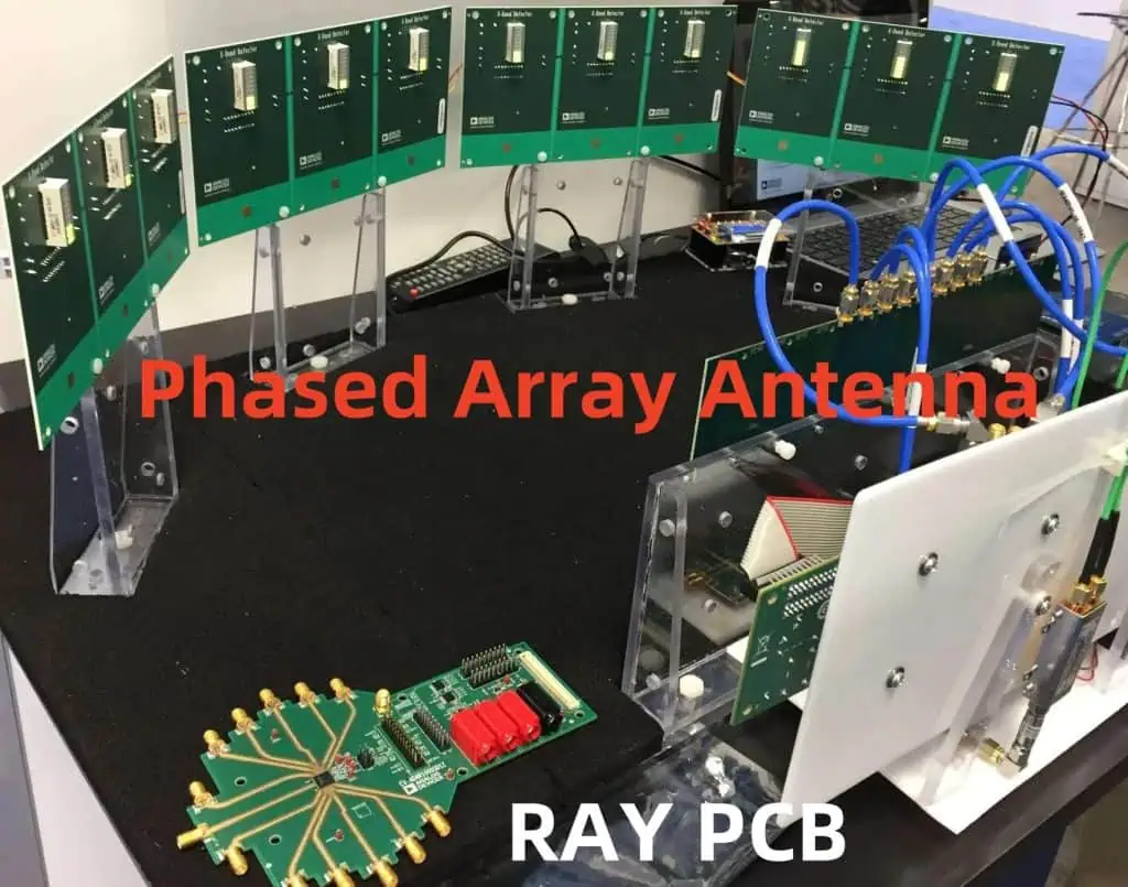
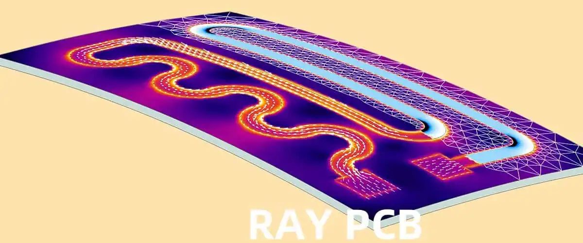
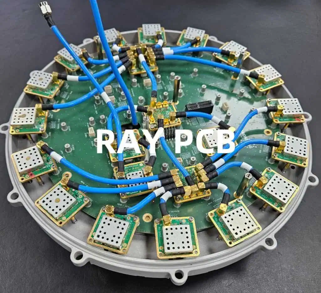
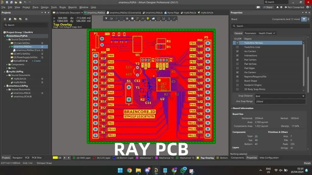
When designing high-frequency and microwave circuits, the choice of the printed circuit board (PCB) structure plays a crucial role in determining the performance, signal integrity, and overall reliability of the system. Two widely used PCB structures in the microwave domain are microstrip and grounded coplanar waveguide (GCPW). In this article, we’ll delve into the fundamentals, advantages, and drawbacks of these structures, providing insights to assist you in making informed decisions for your microwave PCB designs.

YouTube video

Microstrip

Definition and Structure

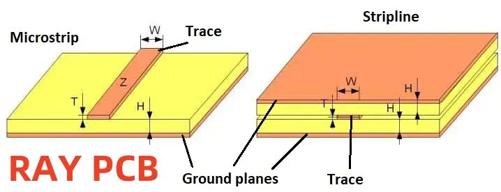
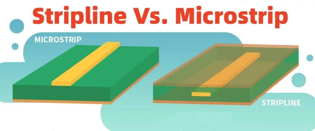
The microstrip is one of the most widely used transmission line structures in microwave PCB design. It consists of a conducting strip (or trace) separated from a ground plane by a dielectric substrate. The conducting strip, also known as the signal line, is typically made of copper or other highly conductive materials.

+-----+
| |
| |
| |
+-----+
|||
|||
+-----+
| |
| |
| |
+-----+

Advantages of Microstrip

  1. Easy Fabrication: Microstrip structures are relatively simple to manufacture, making them cost-effective and widely available.
  2. Compact Size: The compact nature of microstrip allows for dense circuit integration, enabling miniaturization of microwave systems.
  3. Easy Integration: Microstrip lines can be easily integrated with other planar components, such as surface-mount devices (SMDs), making them suitable for monolithic microwave integrated circuits (MMICs).
  4. Shielding: The ground plane provides shielding from external electromagnetic interference (EMI), enhancing signal integrity.

Disadvantages of Microstrip

  1. Dispersion: Microstrip lines exhibit frequency dispersion, where the propagation velocity varies with frequency, potentially distorting signals with wide bandwidths.
  2. Surface Wave Excitation: Microstrip structures can excite surface waves, leading to increased radiation losses and potential crosstalk between adjacent lines.
  3. Limited Bandwidth: Due to the dispersive nature of microstrip, the usable bandwidth is limited, especially at higher frequencies.
  4. Substrate Limitations: The choice of substrate material and thickness can impact the performance of microstrip lines, introducing trade-offs between various parameters.

Grounded Coplanar Waveguide (GCPW)

Definition and Structure

The grounded coplanar waveguide (GCPW) is another popular transmission line structure used in microwave PCB design. It consists of a central signal line sandwiched between two co-planar ground planes, all residing on the same substrate layer.

+-----+-----+-----+
| | | |
| | | |
+-----+-----+-----+
| | | |
| | | |
+-----+-----+-----+

Advantages of GCPW

  1. Low Dispersion: GCPW structures exhibit low dispersion, making them suitable for wideband applications and minimizing signal distortion.
  2. Low Radiation Loss: The ground planes on either side of the signal line help contain the electromagnetic fields, resulting in lower radiation losses compared to microstrip.
  3. Easy Shunt Integration: GCPW allows for easy integration of shunt components, such as capacitors or inductors, directly connected to the signal line and ground planes.
  4. Flexibility in Substrate Choice: GCPW can be implemented on a variety of substrate materials, including low-cost and high-performance options.

Disadvantages of GCPW

  1. Larger Footprint: GCPW structures typically require a larger footprint compared to microstrip, due to the presence of two ground planes.
  2. Potential for Parallel Plate Modes: At higher frequencies, GCPW can excite parallel plate modes, leading to potential signal integrity issues.
  3. Increased Coupling: The close proximity of the signal line to the ground planes can result in increased coupling, which may require careful layout and ground plane shaping.
  4. Sensitivity to Manufacturing Tolerances: GCPW designs can be sensitive to manufacturing tolerances, as small variations in dimensions can significantly impact performance.

Comparison of Key Parameters

Stripline Vs. Microstrip

To better understand the trade-offs between microstrip and GCPW structures, let’s compare some key parameters:

ParameterMicrostripGrounded Coplanar Waveguide (GCPW)Characteristic ImpedanceControlled by strip width, substrate thickness, and dielectric constantControlled by signal line width and gap to ground planesDispersionHigher dispersion, especially at higher frequenciesLower dispersion, suitable for wideband applicationsRadiation LossHigher radiation loss due to fringing fieldsLower radiation loss due to ground plane shieldingCrosstalkHigher potential for crosstalk between adjacent linesLower crosstalk due to ground plane shieldingSubstrate ChoiceLimited substrate options due to impedance matching considerationsMore flexible substrate choice, including low-cost optionsIntegration with ComponentsEasy integration with surface-mount devices (SMDs)Easy integration with shunt components (capacitors, inductors, etc.)Manufacturing ComplexitySimpler fabrication processMore complex fabrication due to ground plane requirements

Design Considerations and Trade-offs

When choosing between microstrip and GCPW structures for your microwave PCB design, several factors must be considered:

  1. Frequency Range: Microstrip is generally preferred for lower frequencies, while GCPW becomes more advantageous at higher frequencies due to its lower dispersion and radiation losses.
  2. Bandwidth Requirements: If your application demands wideband operation or requires minimal signal distortion, GCPW may be the better choice due to its low dispersion characteristics.
  3. Component Integration: Microstrip is well-suited for integrating surface-mount devices, while GCPW excels in integrating shunt components directly to the signal line.
  4. Crosstalk and Isolation: GCPW offers better isolation and reduced crosstalk between adjacent lines, making it advantageous for densely packed designs.
  5. Cost and Complexity: Microstrip is generally more cost-effective and simpler to fabricate, while GCPW may require more complex manufacturing processes and potentially higher costs.
  6. Substrate Availability and Performance: The choice between microstrip and GCPW may also depend on the availability and performance characteristics of the substrate materials you plan to use.

Ultimately, the decision between microstrip and GCPW should be based on a careful evaluation of your specific design requirements, performance targets, and constraints, such as cost, size, and manufacturing capabilities.

Frequently Asked Questions (FAQ)

  1. Q: Can microstrip and GCPW structures be combined in the same design? A: Yes, it is possible to combine microstrip and GCPW structures within the same design. This approach can leverage the strengths of each structure while mitigating their respective weaknesses. However, proper transitions between the two structures must be carefully designed to minimize signal reflections and ensure optimal performance.
  2. Q: Which structure is better suited for high-power applications? A: GCPW structures are generally better suited for high-power applications due to their improved heat dissipation capabilities and lower radiation losses. The ground planes in GCPW provide better heat spreading and shielding, making them more suitable for handling higher power levels.
  3. Q: How do manufacturing tolerances affect microstrip and GCPW performance? A: Manufacturing tolerances can have a significant impact on the performance of both microstrip and GCPW structures. Microstrip is generally more forgiving to minor variations in dimensions, while GCPW is more sensitive due to the tight coupling between the signal line and ground planes. Careful consideration of manufacturing tolerances is crucial during the design phase.
  4. Q: Can GCPW structures be used for high-speed digital signals? A: Yes, GCPW structures can be used for high-speed digital signals, particularly in applications where low dispersion and low radiation losses are critical. The low dispersion characteristics of GCPW help maintain signal integrity over a wide bandwidth, making it suitable for high-speed digital communications.
  5. Q: Are there any alternative transmission line structures besides microstrip and GCPW? A: While microstrip and GCPW are the most commonly used transmission line structures in microwave PCB design, there are several alternative structures, such as stripline, suspended stripline, and coplanar waveguide (CPW). Each structure

DIY Constant Current Dummy Load for Power Supply and Battery Testing

Building a constant current dummy load is an essential tool for anyone working with power supplies, batteries, or other electrical devices. This device allows you to test and evaluate the performance of your power source under controlled load conditions. Whether you’re troubleshooting a faulty power supply, calibrating a new one, or simply testing the capacity of a battery, a constant current dummy load is an invaluable asset.

In this article, we’ll guide you through the process of building your own constant current dummy load, step-by-step. We’ll cover the necessary components, circuit design, and construction techniques, ensuring that you end up with a reliable and accurate testing instrument.

YouTube video

Benefits of a Constant Current Dummy Load

Before diving into the nitty-gritty of the build process, let’s take a moment to understand the benefits of having a constant current dummy load in your arsenal:

  1. Power Supply Testing: With a constant current dummy load, you can accurately test the performance of your power supplies under various load conditions. This is particularly useful for verifying the output voltage regulation, ripple, and overall stability of the power supply.
  2. Battery Capacity Testing: A constant current dummy load is invaluable for testing the capacity and discharge characteristics of batteries. By applying a controlled, constant load, you can determine the true capacity of your batteries and identify any potential issues.
  3. Circuit Debugging: When troubleshooting electronic circuits, a constant current dummy load can help you isolate and identify potential problems by simulating different load conditions.
  4. Calibration and Verification: Many electronic devices require precise calibration, and a constant current dummy load can assist in this process by providing a known, stable load for calibration purposes.
  5. Safety: By using a dummy load, you can safely test and evaluate your power sources without the risk of damaging sensitive components or creating potential hazards.

Circuit Design

The heart of a constant current dummy load is a circuit that can maintain a constant current draw, regardless of the applied voltage. While there are several approaches to achieving this, we’ll focus on a simple and effective design that utilizes a handful of readily available components.

Components Required

ComponentDescription
Power ResistorA high-power resistor capable of dissipating the desired load current (e.g., 50W, 100W, or higher, depending on your needs)
Operational Amplifier (Op-Amp)A general-purpose op-amp, such as the LM358 or LM324
TransistorA high-power transistor, such as the TIP3055 or equivalent
PotentiometerA multi-turn potentiometer for adjusting the load current
ResistorsVarious resistor values for biasing and feedback (e.g., 10K, 1K, etc.)
CapacitorsCapacitors for decoupling and stability (e.g., 0.1uF, 10uF)
HeatsinkA suitable heatsink for the power resistor and transistor
EnclosureBanana plugs, binding posts, or other connectors for input and output

Before we dive into the circuit details, let’s gather the necessary components:

Schematic and Circuit Explanation

The constant current dummy load circuit is based on a simple op-amp configuration, known as a “current sink.” Here’s a breakdown of how it works:

                   +V
|
|
R1
|
|
+-------+-----+
| | |
| | |
-+- | |
| | |
| | |
| Z |
| E |
| M |
| P |
| E |
| | |
| V |
| | |
+---------+---+
|
|
R2
|
|
-V
  1. The op-amp (U1) is configured as a voltage follower, with its non-inverting input (+) connected to the wiper of the potentiometer (R3).
  2. The inverting input (-) of the op-amp is connected to the emitter of the transistor (Q1) through a feedback resistor (R2). This forms a negative feedback loop, which helps maintain a constant current through the load (R_LOAD).
  3. The potentiometer (R3) is used to set the desired load current by adjusting the voltage at the non-inverting input of the op-amp.
  4. The transistor (Q1) acts as a variable resistor, controlled by the op-amp output. As the op-amp adjusts its output voltage to maintain the set current, the transistor’s resistance changes accordingly.
  5. The power resistor (R_LOAD) is the actual dummy load, dissipating the power from the power source under test.
  6. Resistor R1 and the bypass capacitors (C1, C2) are used for biasing and stability, respectively.

By adjusting the potentiometer (R3), you can set the desired load current, and the circuit will automatically maintain that current level, regardless of the input voltage (within the operational limits of the components).

Construction and Assembly

Now that you understand the circuit design, it’s time to build your constant current dummy load. Here are the steps to follow:

  1. Obtain the Components: Gather all the necessary components listed in the previous section. Make sure to select high-quality components that can handle the expected power dissipation and current levels.
  2. Prepare the Enclosure: Choose a suitable enclosure to house your circuit. Metal enclosures are preferred for their superior heat dissipation capabilities, but plastic enclosures can also work if adequate ventilation is provided.
  3. Mount the Components: Carefully mount the components onto a prototyping board or a custom-made printed circuit board (PCB). Follow good electronics assembly practices, such as proper lead routing, adequate spacing, and heat sinking for high-power components.
  4. Wiring and Connections: Connect the components according to the schematic diagram. Use appropriate wire gauges and make secure, reliable connections.
  5. Heatsink Installation: Attach the power resistor and transistor to a suitable heatsink using thermal paste or adhesive. Proper heat dissipation is crucial for the safe operation of your dummy load.
  6. Enclosure Assembly: Once all the components are mounted and wired, carefully place the assembly into the enclosure, ensuring proper clearances and ventilation.
  7. Input and Output Connections: Install the necessary connectors (e.g., banana plugs, binding posts) for the input and output connections. Clearly label the positive and negative terminals.
  8. Testing and Calibration: After assembly, carefully test your constant current dummy load to ensure proper operation. Use a power supply or battery source to verify the load current at various settings. Adjust the potentiometer and observe the current readings on a multimeter or ammeter.
  9. Final Touches: Once everything is working as expected, you can add finishing touches like labels, markings, or a protective cover for the potentiometer.

Remember, safety should be your top priority when working with high-power circuits. Always use proper insulation, follow safety guidelines, and never exceed the rated power dissipation of your components.

Usage and Applications

With your newly built constant current dummy load, you can tackle a wide range of testing and evaluation tasks. Here are some common applications:

  1. Power Supply Testing: Connect your power supply to the dummy load and adjust the load current to various levels. Observe the output voltage regulation, ripple, and stability under different load conditions.
  2. Battery Capacity Testing: Hook up your battery to the dummy load and set the desired load current. Monitor the battery voltage over time to determine its capacity and discharge characteristics.
  3. Circuit Debugging: Use the dummy load to simulate different load conditions on your electronic circuits, helping you identify and isolate potential issues.
  4. Calibration and Verification: Utilize the constant current load as a reference for calibrating and verifying the accuracy of other instruments, such as ammeters or power analyzers.
  5. Burn-in Testing: Subject your power supplies or electronic devices to extended periods of controlled load conditions to identify potential failures or weaknesses.

Remember, always start with lower load currents and gradually increase them, ensuring that you stay within the safe operating limits of your device under test and the dummy load itself.

Flight Control System Design: Hardware and PCB Design By KiCAD

In the dynamic world of aerospace engineering, the design and development of reliable and efficient flight control systems are paramount to ensuring safe and precise aircraft operation. These complex systems require a harmonious integration of hardware, software, and electronics components, making the hardware and Printed Circuit Board (PCB) design process a critical aspect. KiCAD, an open-source suite of tools for electronic design automation (EDA), has emerged as a powerful solution for designing flight control systems, offering a comprehensive set of features for schematic capture, PCB layout, and simulation.

This article explores the intricacies of flight control system design, focusing on the hardware and PCB aspects using KiCAD. We will delve into the essential components, design considerations, and best practices that engineers should understand when developing these intricate systems. Additionally, we will highlight the advantages of using KiCAD and its various tools for streamlining the design process.

YouTube video

Understanding Flight Control Systems

Flight control systems are responsible for maintaining the stability, maneuverability, and desired flight path of an aircraft. These systems typically consist of three main components:

  1. Sensors: Sensors collect data related to the aircraft’s attitude, altitude, airspeed, and other relevant parameters. Common sensors used in flight control systems include gyroscopes, accelerometers, pitot tubes, and GPS receivers.
  2. Control Computers: Control computers, often microcontrollers or embedded systems, process the sensor data and execute algorithms to determine the appropriate control actions.
  3. Actuators: Actuators, such as servos or hydraulic systems, translate the control commands into physical movements of the aircraft’s control surfaces (e.g., ailerons, elevators, and rudder).

The hardware and PCB design play a crucial role in integrating these components and ensuring reliable and efficient operation of the flight control system.

Hardware Design Considerations

When designing the hardware for a flight control system, several factors must be taken into account:

1. Sensor Integration

Proper sensor integration is vital for accurate data acquisition. Engineers must consider factors such as sensor placement, shielding, and signal conditioning to minimize noise and interference. Additionally, the sensor interfaces (e.g., I2C, SPI, or analog) must be compatible with the control computer.

2. Microcontroller Selection

The microcontroller or embedded system serves as the brain of the flight control system. Selection criteria include computational power, memory capacity, peripheral interfaces, and real-time performance. Common microcontrollers used in flight control systems include ARM Cortex-M series and Atmel AVR microcontrollers.

3. Power Management

Efficient power management is essential for flight control systems, especially in battery-powered aircraft. Designers must consider power consumption, voltage regulation, and power distribution to ensure reliable operation and extend battery life.

4. Environmental Considerations

Flight control systems must operate in harsh environments, including varying temperatures, vibrations, and electromagnetic interference (EMI). Hardware design should incorporate measures such as thermal management, shock and vibration isolation, and EMI shielding to ensure reliable operation.

5. Redundancy and Fail-Safe Mechanisms

Safety is a critical aspect of flight control systems. Redundant components, watchdog timers, and fail-safe mechanisms should be implemented to prevent catastrophic failures and maintain control in the event of component malfunctions.

PCB Design Using KiCAD

KiCAD is a powerful open-source EDA suite that provides a comprehensive set of tools for PCB design, including schematic capture, PCB layout, and simulation. Here’s how KiCAD can be leveraged for flight control system PCB design:

1. Schematic Capture

KiCAD’s Eeschema component allows for the creation of schematics by placing components and interconnecting them with wires and buses. Engineers can create hierarchical schematics, assign footprints to components, and perform electrical rule checks (ERCs) to ensure design integrity.

2. PCB Layout

Pcbnew, KiCAD’s PCB layout tool, enables engineers to transform schematics into physical PCB layouts. Features such as automatic track routing, differential pair routing, and interactive length tuning simplify the layout process. Additionally, KiCAD supports various design rules and constraints to ensure manufacturability.

3. Libraries and Component Management

KiCAD offers extensive component libraries, including standard components and user-defined libraries. Engineers can create custom footprints and symbols for specialized components, ensuring accurate representation and integration into the design.

4. Simulation and Verification

KiCAD’s simulation capabilities, including SPICE integration and signal integrity analysis, allow for pre-manufacturing verification of the design. Engineers can simulate and analyze the behavior of analog and digital circuits, ensuring proper functionality and identifying potential issues before prototyping.

5. 3D Visualization and STEP Integration

KiCAD’s 3D viewer and STEP integration enable engineers to visualize the PCB design in a 3D environment, facilitating mechanical integration and ensuring proper fit within the aircraft’s structure.

6. Manufacturing Output

KiCAD supports various manufacturing output formats, including Gerber files, drill files, and pick-and-place files. This streamlines the transition from design to manufacturing, enabling efficient collaboration with PCB fabrication and assembly services.

Design Workflow and Best Practices

When designing flight control systems using KiCAD, it is essential to follow a structured workflow and adhere to best practices to ensure a successful outcome:

1. Requirements Gathering and Planning

Begin by clearly defining the system requirements, including performance specifications, environmental conditions, and safety standards. Develop a comprehensive design plan that outlines the hardware architecture, component selection, and design constraints.

2. Schematic Capture and Component Selection

Create detailed schematics in KiCAD’s Eeschema, carefully selecting components that meet the design requirements. Ensure proper component footprint assignment and perform electrical rule checks to validate the schematic.

3. PCB Layout and Routing

Translate the schematic into a physical PCB layout using Pcbnew. Follow best practices for component placement, routing, and signal integrity. Utilize KiCAD’s design rule checks and constraint management tools to ensure manufacturability.

4. Simulation and Verification

Leverage KiCAD’s simulation capabilities to verify the design before prototyping. Perform circuit simulations, signal integrity analysis, and electromagnetic compatibility (EMC) analysis to identify and address potential issues.

5. Prototyping and Testing

Once the design is verified through simulation, create prototypes pcba for thorough testing and validation. Test the flight control system in relevant environmental conditions and perform functional tests to ensure compliance with system requirements.

6. Iteration and Refinement

Based on the test results, iterate and refine the design as necessary. Update the schematics, PCB layout, and simulations to incorporate improvements and address any identified issues.

7. Manufacturing and Integration

When the design is finalized, generate the necessary manufacturing output files (e.g., Gerber files, drill files) and engage with PCB fabrication and assembly services. Ensure proper integration of the PCB into the aircraft’s structure and system.

8. Documentation and Version Control

Maintain comprehensive documentation throughout the design process, including design specifications, test reports, and assembly instructions. Implement version control practices to track changes and facilitate collaboration within the engineering team.

Advantages of Using KiCAD for Flight Control System Design

Choosing KiCAD for flight control system design offers several advantages:

  1. Open-Source and Cost-Effective: As an open-source EDA suite, KiCAD provides a cost-effective solution for hardware and PCB design, making it accessible to organizations of various sizes and budgets.
  2. Cross-Platform Compatibility: KiCAD is available for multiple operating systems, including Windows, macOS, and Linux, ensuring flexibility and compatibility across different development environments.
  3. Community Support and Resources: KiCAD has a large and active community of users and developers, providing access to extensive documentation, tutorials, and support forums, facilitating knowledge sharing and problem-solving.
  4. Customizability and Extensibility: KiCAD’s modular architecture and scripting capabilities allow for customization and integration with third-party tools, enabling engineers to tailor the design environment to their specific needs.
  5. Comprehensive Feature Set: KiCAD offers a wide range of features, including schematic capture, PCB layout, simulation, and manufacturing output, providing a complete solution for flight control system design.
  6. Interoperability and Data Exchange: KiCAD supports various file formats for data exchange, enabling seamless collaboration with other EDA tools and integration into existing design workflows.

The reasons to consider PIM when designing a PCB antenna.

2.4 ghz pcb antenna design

In the ever-evolving world of wireless communication systems, the design of Printed Circuit Board (PCB) antennas has become increasingly crucial. These compact and efficient antennas play a vital role in enabling seamless connectivity and reliable data transmission. However, one critical factor that must be considered during the PCB antenna design process is Passive Intermodulation (PIM). PIM can significantly impact the performance and reliability of RF systems, making it essential for engineers to understand and address this phenomenon effectively.

This comprehensive article delves into the reasons why PIM should be a top priority when designing PCB antennas. We will explore the fundamentals of PIM, its sources, and its effects on wireless communication systems. Additionally, we will discuss various strategies and techniques for mitigating PIM and optimizing PCB antenna performance.

YouTube video

Understanding Passive Intermodulation (PIM)

Passive Intermodulation (PIM) is a non-linear phenomenon that occurs when two or more high-power signals interact with non-linear materials or components within a Radio Frequency (RF) system. This interaction generates unwanted intermodulation products, which can interfere with the desired signals, causing degradation in system performance and potentially leading to communication disruptions.

Sources of PIM

PIM can originate from various sources within an RF system, including:

  1. Non-linear materials: Certain materials, such as ferromagnetic metals, can exhibit non-linear behavior when exposed to high-power RF signals, leading to the generation of PIM products.
  2. Imperfect connections: Loose or corroded connections within the RF system can introduce non-linearities, acting as potential PIM sources.
  3. Component defects: Manufacturing defects or impurities in components like connectors, cables, and antennas can contribute to PIM generation.
  4. Oxidation and corrosion: Over time, the exposure of metallic surfaces to environmental factors like moisture, salt, and pollutants can lead to oxidation and corrosion, increasing the risk of PIM.

Effects of PIM on RF Systems

PIM can have detrimental effects on the performance of wireless communication systems, including:

  1. Reduced system sensitivity: PIM products can act as interference, reducing the system’s ability to detect and decode desired signals accurately.
  2. Decreased coverage and capacity: The presence of PIM can limit the effective range and capacity of a wireless network, leading to reduced performance and potential coverage gaps.
  3. Increased interference: PIM products can interfere with other systems operating in the same frequency band, causing disruptions and potential regulatory compliance issues.
  4. Degraded quality of service: The impact of PIM can result in lower data rates, higher latency, and reduced quality of service for end-users.

Importance of Considering PIM in PCB Antenna Design

PCB Antenna Layout
PCB Antenna Layout

PCB antennas are widely used in various wireless communication systems due to their compact size, low cost, and ease of integration. However, the design of these antennas can significantly influence the generation and impact of PIM. Several factors contribute to the importance of considering PIM during the PCB antenna design process:

1. Antenna Geometry and Materials

The geometry and materials used in the construction of PCB antennas can play a crucial role in PIM generation. Non-linear materials or irregularities in the antenna structure can act as potential PIM sources, compromising the overall system performance.

2. Antenna Placement and Surrounding Environment

The placement of the PCB antenna within the device or system, as well as its proximity to other components and materials, can affect the level of PIM generated. Environmental factors like temperature, humidity, and exposure to contaminants can also influence PIM behavior.

3. Frequency of Operation

Different frequency bands may exhibit varying levels of PIM sensitivity. As the frequency increases, the impact of PIM can become more pronounced, making it critical to consider PIM mitigation strategies during the design phase.

4. System Requirements and Standards

Many wireless communication systems and standards have specific requirements and guidelines related to PIM performance. Failing to consider PIM during the PCB antenna design stage can lead to non-compliance with these standards, potentially resulting in regulatory issues or system performance degradation.

5. Cost and Time Savings

Addressing PIM at the early stages of PCB antenna design can save significant time and costs compared to resolving PIM issues after the product has been manufactured and deployed. Proactive PIM mitigation can prevent costly redesigns, rework, and system performance issues in the field.

Strategies for PIM Mitigation in PCB Antenna Design

To effectively address PIM in PCB antenna design, engineers can employ various strategies and techniques. These include:

1. Material Selection

Carefully selecting the materials used in the construction of PCB antennas is crucial for minimizing PIM generation. Non-linear materials, such as ferromagnetic metals, should be avoided whenever possible. Alternatively, materials with low PIM characteristics, like aluminum or copper, can be used.

2. Antenna Geometry Optimization

The geometry of the PCB antenna can be optimized to reduce the potential for PIM generation. This may involve minimizing sharp edges, avoiding abrupt transitions, and ensuring a smooth current flow within the antenna structure.

3. PCB Design Considerations

The layout and design of the PCB itself can impact PIM performance. Proper grounding and shielding techniques, as well as careful component placement and routing, can help mitigate PIM sources. Additionally, incorporating PIM-optimized connectors and transmission lines can further improve PIM performance.

4. PIM Testing and Characterization

Conducting thorough PIM testing and characterization during the design and prototyping phases is essential for identifying and addressing potential PIM issues. This may involve specialized PIM testing equipment and methodologies to accurately measure and analyze PIM levels.

5. Environmental Considerations

Accounting for the environmental conditions in which the PCB antenna will operate is crucial for effective PIM mitigation. Factors such as temperature, humidity, and exposure to contaminants should be considered, and appropriate protective measures or materials should be employed to minimize their impact on PIM generation.

6. System-Level Optimization

In addition to optimizing the PCB antenna design, a system-level approach may be necessary to mitigate PIM effectively. This can involve optimizing the entire RF signal chain, including filters, amplifiers, and other components, to minimize the potential for PIM generation and propagation.

Frequently Asked Questions (FAQs)

1. What is the primary cause of PIM in PCB antennas?

The primary cause of PIM in PCB antennas is the non-linear behavior of materials or components when exposed to high-power RF signals. This non-linearity can lead to the generation of unwanted intermodulation products, which can interfere with the desired signals.

2. How does PIM affect the performance of wireless communication systems?

PIM can have detrimental effects on the performance of wireless communication systems, including reduced system sensitivity, decreased coverage and capacity, increased interference, and degraded quality of service for end-users.

3. Why is it important to consider PIM during the PCB antenna design stage?

Considering PIM during the PCB antenna design stage is crucial because the antenna’s geometry, materials, and placement can significantly influence the generation and impact of PIM. Addressing PIM early in the design process can save time, costs, and ensure compliance with system requirements and standards.

4. What are some strategies for mitigating PIM in PCB antenna design?

Strategies for mitigating PIM in PCB antenna design include careful material selection, antenna geometry optimization, PCB design considerations (e.g., grounding, shielding, component placement), PIM testing and characterization, environmental considerations, and system-level optimization.

5. How can PIM testing and characterization help in PCB antenna design?

PIM testing and characterization during the design and prototyping phases are essential for identifying and addressing potential PIM issues. This involves specialized PIM testing equipment and methodologies to accurately measure and analyze PIM levels, allowing for targeted optimization and mitigation strategies.

Conclusion

Passive Intermodulation (PIM) is a critical factor that must be considered when designing PCB antennas for wireless communication systems. The potential impact of PIM on system performance, including reduced sensitivity, decreased coverage and capacity, increased interference, and degraded quality of service, highlights the importance of addressing this phenomenon effectively.

By understanding the sources of PIM, its effects on RF systems, and the strategies for PIM mitigation, engineers can develop PCB antennas that offer superior performance and reliability. From material selection and antenna geometry optimization to environmental considerations and system-level optimization, a comprehensive approach is necessary to mitigate PIM and ensure compliance with system requirements and standards.

Incorporating PIM mitigation strategies into the PCB antenna

How is Fluke 233 Multimeter Useful for Electronics Engineers

Keywords: Fluke 233 Multimeter, Electronics Engineering, Multimeter Features, Electrical Measurements, Troubleshooting, Repair, Maintenance

Introduction

In the field of electronics engineering, having the right tools is essential for efficient and accurate work. One such tool that has become indispensable for electronics engineers is the Fluke 233 Multimeter. This highly versatile and reliable instrument is designed to meet the diverse needs of professionals who work with electrical circuits, systems, and components. Whether you’re involved in design, testing, troubleshooting, or maintenance, the Fluke 233 Multimeter can be a valuable asset in your toolkit.

YouTube video

Fluke 233 Multimeter: An Overview

The Fluke 233 Multimeter is a compact and rugged digital multimeter that combines advanced features with user-friendly operation. Manufactured by Fluke Corporation, a renowned name in the world of test equipment, this multimeter is built to withstand harsh environments and provide reliable measurements in various applications.

Key Features

  • Wide Range of Measurements: The Fluke 233 Multimeter is capable of measuring a wide range of electrical parameters, including AC/DC voltage, AC/DC current, resistance, capacitance, frequency, and temperature.
  • True RMS Readings: The multimeter features True RMS (Root Mean Square) technology, which ensures accurate readings even when measuring non-linear signals or waveforms with high harmonic content.
  • Automatic and Manual Ranging: The Fluke 233 Multimeter offers both automatic and manual ranging capabilities, allowing you to choose the appropriate range for your measurement needs.
  • Data Hold and Min/Max/Avg Recording: The multimeter has a data hold function that freezes the displayed reading, making it easier to record or analyze measurements. Additionally, it can record minimum, maximum, and average values over a specific time period.
  • Backlit Display: The large, backlit display ensures clear visibility of measurement readings, even in low-light conditions.
  • Safety Features: The Fluke 233 Multimeter is designed with safety in mind, featuring overvoltage protection, input alert, and compliance with relevant safety standards.

Applications in Electronics Engineering

The Fluke 233 Multimeter finds application in various areas of electronics engineering, making it a valuable tool for professionals in this field.

1. Circuit Design and Prototyping

During the circuit design and prototyping phase, electronics engineers need to take precise measurements to ensure the proper functioning of their circuits. The Fluke 233 Multimeter’s ability to measure voltage, current, resistance, and other parameters with high accuracy makes it an essential tool for verifying circuit performance and identifying potential issues before moving to the production stage.

2. Troubleshooting and Repair

One of the primary applications of the Fluke 233 Multimeter is in troubleshooting and repair of electronic devices and systems. When faced with a malfunctioning circuit or component, electronics engineers can use the multimeter to isolate the problem by taking measurements at various points in the circuit. The True RMS capability of the Fluke 233 Multimeter ensures accurate readings, even when dealing with complex waveforms, which is crucial for identifying and resolving issues efficiently.

3. Maintenance and Testing

Regular maintenance and testing are essential for ensuring the reliable operation of electronic systems and equipment. Electronics engineers can use the Fluke 233 Multimeter to perform routine checks, measure voltage levels, test components, and verify the functionality of various circuits. The multimeter’s rugged design and safety features make it suitable for use in harsh environments, such as industrial settings or field service applications.

4. Educational and Training Purposes

In educational settings, such as universities and technical institutes, the Fluke 233 Multimeter can be an invaluable teaching tool for electronics engineering courses. Its user-friendly interface and comprehensive measurement capabilities make it an ideal choice for hands-on learning and practical demonstrations. Students can gain practical experience in taking accurate measurements, analyzing circuit behavior, and troubleshooting techniques using this multimeter.

Measurement Capabilities

The Fluke 233 Multimeter offers a wide range of measurement capabilities, making it a versatile tool for electronics engineers. Here are some of the key measurements that can be performed with this multimeter:

These measurement capabilities cover a wide range of applications, allowing electronics engineers to analyze and troubleshoot various circuits and components effectively.

Frequently Asked Questions (FAQs)

1. What is the maximum voltage rating of the Fluke 233 Multimeter?

The Fluke 233 Multimeter can measure up to 600 V AC or DC, making it suitable for most electronics engineering applications. However, it is important to follow proper safety precautions and procedures when working with high voltages.

2. Can the Fluke 233 Multimeter measure current in both AC and DC circuits?

Yes, the Fluke 233 Multimeter can measure both AC and DC current. It has separate ranges for AC and DC current measurements, ensuring accurate readings in both types of circuits.

3. How does the True RMS feature benefit electronics engineers?

The True RMS (Root Mean Square) feature of the Fluke 233 Multimeter ensures accurate measurements of non-linear signals or waveforms with high harmonic content. This is particularly important in electronics engineering, where many circuits and components produce complex waveforms that would be inaccurately measured by multimeters without True RMS capability.

4. Can the Fluke 233 Multimeter be used for temperature measurements?

Yes, the Fluke 233 Multimeter can measure temperature when used in conjunction with a compatible temperature probe (not included). This capability can be useful for electronics engineers working with temperature-sensitive components or systems.

5. What safety features does the Fluke 233 Multimeter offer?

The Fluke 233 Multimeter is designed with several safety features, including overvoltage protection, input alert, and compliance with relevant safety standards. These features help protect the user and the multimeter itself from potential hazards during measurements.

Conclusion

The Fluke 233 Multimeter is a versatile and reliable tool that offers a comprehensive range of measurement capabilities essential for electronics engineering. Its robust design, advanced features, and user-friendly interface make it an invaluable asset for circuit design, prototyping, troubleshooting, repair, maintenance, and educational purposes. With its True RMS technology, automatic and manual ranging options, data hold and recording functions, and safety features, the Fluke 233 Multimeter provides electronics engineers with the precision and flexibility they need to tackle a wide range of tasks efficiently and accurately.

Reducing Active Device Temperature Rise and RF Heating Effects with Low Loss Circuit Laminates

As electronic devices become increasingly compact and powerful, the issue of heat dissipation has emerged as a critical challenge. Active components, such as processors, amplifiers, and radio frequency (RF) circuits, generate substantial amounts of heat during operation, which can lead to performance degradation, reliability issues, and even catastrophic failure if not properly managed. This problem is further exacerbated by the growing demand for higher frequencies in wireless communication systems, where RF heating effects can significantly impact signal integrity and power efficiency.

Effective heat management is crucial for ensuring the reliable and efficient operation of electronic devices, particularly those used in mission-critical applications or harsh environments. One promising solution to this challenge lies in the use of low loss circuit laminates, which offer superior thermal and electrical properties compared to traditional materials.

YouTube video

Thermal Management Challenges in Electronic Devices

Active Device Temperature Rise

Active devices, such as processors, power amplifiers, and RF transceivers, generate substantial amounts of heat during operation due to the inherent losses associated with their electrical and thermal characteristics. As these devices become more powerful and densely integrated, the heat dissipation challenge becomes increasingly severe.

Excessive temperature rise in active devices can have detrimental effects on their performance, reliability, and lifespan. High temperatures can lead to increased leakage currents, decreased carrier mobility, and accelerated electromigration, all of which contribute to performance degradation and potential device failure.

RF Heating Effects

In wireless communication systems, RF heating effects can significantly impact signal integrity and power efficiency. RF signals, particularly at higher frequencies, can induce currents in nearby conductors and dielectric materials, leading to the generation of heat through resistive losses.

RF heating can cause several issues, including:

  1. Signal attenuation and distortion due to increased dielectric losses and conductor resistance.
  2. Thermal expansion and deformation of materials, leading to changes in circuit dimensions and characteristics.
  3. Increased power consumption and reduced efficiency due to heat-related losses.

These effects become increasingly problematic as wireless systems operate at higher frequencies and higher power levels, necessitating the use of materials with superior thermal and electrical properties.

Low Loss Circuit Laminates: A Solution to Thermal Challenges

Low loss circuit laminates are advanced composite materials designed to address the thermal and electrical challenges faced by modern electronic devices. These laminates are engineered to exhibit exceptional thermal conductivity, low dielectric loss, and high dimensional stability, making them well-suited for applications where heat dissipation and signal integrity are critical.

Superior Thermal Conductivity

One of the key advantages of low loss circuit laminates is their high thermal conductivity, which allows for efficient heat transfer away from active components. This property is achieved through the incorporation of thermally conductive fillers, such as ceramics or metallic particles, into the laminate’s composition.

By facilitating effective heat dissipation, low loss circuit laminates help maintain active device temperatures within acceptable limits, ensuring reliable operation and prolonged lifespan.

Low Dielectric Loss

Low loss circuit laminates are designed to exhibit low dielectric loss, a property that minimizes signal attenuation and power dissipation in high-frequency applications. This is achieved through the careful selection of dielectric materials and the optimization of their composition and structure.

By reducing dielectric losses, these laminates ensure better signal integrity, lower power consumption, and improved efficiency in RF and high-speed digital circuits.

High Dimensional Stability

Dimensional stability is another critical characteristic of low loss circuit laminates. These materials are engineered to maintain their physical dimensions and electrical properties over a wide range of temperatures and environmental conditions.

This stability is crucial for ensuring the reliability and repeatability of circuit performance, as dimensional changes can lead to shifts in component values, impedance mismatches, and signal degradation.

Applications of Low Loss Circuit Laminates

rogers board

Low loss circuit laminates find applications in a wide range of industries and applications where thermal management and signal integrity are of paramount importance. Some key areas of application include:

Telecommunications

The telecommunications industry relies heavily on high-frequency RF systems for wireless communication. Low loss circuit laminates are essential for ensuring efficient signal transmission, minimizing power losses, and maintaining system reliability in base stations, small cells, and other telecommunications infrastructure.

Aerospace and Defense

Electronic systems used in aerospace and defense applications are often subjected to extreme temperatures and harsh environmental conditions. Low loss circuit laminates provide the necessary thermal management capabilities and dimensional stability to ensure reliable operation in these demanding environments.

Automotive Electronics

Modern automotive electronics, such as advanced driver assistance systems (ADAS), infotainment systems, and radar modules, require efficient heat dissipation and signal integrity. Low loss circuit laminates are crucial for enabling these systems to function reliably under various operating conditions.

Industrial Electronics

Industrial electronics, including motor drives, control systems, and automation equipment, often operate in harsh environments and generate significant amounts of heat. Low loss circuit laminates help ensure reliable operation and prolonged equipment lifespan in these applications.

Design Considerations for Low Loss Circuit Laminates

When designing electronic systems that incorporate low loss circuit laminates, several factors must be considered to optimize thermal management and signal integrity. These include:

Laminate Material Selection

Selecting the appropriate low loss circuit laminate material is crucial for meeting the specific requirements of the application. Factors such as operating frequency, thermal load, and environmental conditions must be taken into account. Common low loss laminate materials include polytetrafluoroethylene (PTFE), hydrocarbon-based laminates, and ceramic-filled composites.

Thermal Design

Effective thermal design is essential for maximizing the benefits of low loss circuit laminates. This may involve the incorporation of heat sinks, thermal vias, and dedicated heat dissipation pathways to facilitate efficient heat transfer away from active components.

Signal Integrity Optimization

To ensure optimal signal integrity, careful consideration must be given to the layout and routing of high-frequency signals on low loss circuit laminates. Techniques such as impedance matching, controlled impedance routing, and minimizing signal path lengths can help mitigate signal degradation and losses.

Environmental Considerations

In applications where electronic systems are exposed to harsh environments, such as extreme temperatures, moisture, or vibrations, the robustness and reliability of low loss circuit laminates become critical. Proper material selection, encapsulation, and environmental testing are necessary to ensure reliable operation under these conditions.

Frequently Asked Questions (FAQs)

  1. What are the main advantages of using low loss circuit laminates? Low loss circuit laminates offer several key advantages, including superior thermal conductivity for efficient heat dissipation, low dielectric loss for improved signal integrity and reduced power consumption, and high dimensional stability for reliable circuit performance under various operating conditions.
  2. How do low loss circuit laminates compare to traditional materials in terms of thermal management? Low loss circuit laminates outperform traditional materials, such as FR-4 laminates, in terms of thermal management capabilities. They exhibit significantly higher thermal conductivity, allowing for more effective heat transfer away from active components, thereby reducing temperature rise and associated performance degradation.
  3. Can low loss circuit laminates be used in high-frequency applications? Yes, low loss circuit laminates are well-suited for high-frequency applications, particularly in the radio frequency (RF) and microwave ranges. Their low dielectric loss characteristics minimize signal attenuation and power dissipation, ensuring better signal integrity and efficiency in these applications.
  4. Are low loss circuit laminates more expensive than traditional materials? Generally, low loss circuit laminates are more expensive than traditional materials like FR-4 laminates. However, the additional cost is often justified by the superior performance, reliability, and lifespan of electronic systems that incorporate these advanced materials.
  5. How do environmental factors affect the performance of low loss circuit laminates? Environmental factors, such as temperature, moisture, and vibrations, can impact the performance of low loss circuit laminates. Proper material selection, encapsulation, and environmental testing are crucial to ensure reliable operation under harsh conditions. Additionally, the dimensional stability of these laminates helps mitigate issues related to thermal expansion and contraction.

How to Drive High Power LEDs With A DC-DC Adjustable Step-Down Module

Light-emitting diodes (LEDs) have become an integral part of modern electronics, offering energy efficiency, durability, and versatility in various applications. However, driving high-power LEDs can be a challenging task, as they require precise voltage and current regulation to ensure optimal performance and longevity. This is where DC-DC adjustable step-down modules come into play, providing a reliable and cost-effective solution for powering high-power LEDs.

YouTube video

In this comprehensive article, we will explore the fundamentals of driving high-power LEDs with a DC-DC adjustable step-down module. We will cover the theoretical aspects, practical considerations, and step-by-step instructions to help you achieve a successful LED lighting setup.

Understanding High-Power LEDs

What are High-Power LEDs?

High-power LEDs, also known as high-brightness LEDs or power LEDs, are a specific type of LED designed to produce a significantly higher amount of light output compared to standard LEDs. These LEDs are capable of delivering luminous intensities ranging from a few hundred to several thousand lumens, making them suitable for various applications such as:

  • Automotive lighting (headlights, taillights, and interior lighting)
  • Architectural and landscape lighting
  • Stage and studio lighting
  • Industrial and commercial lighting

Characteristics of High-Power LEDs

High-power LEDs exhibit several unique characteristics that set them apart from standard LEDs:

  1. High Current Requirement: High-power LEDs typically operate at higher current levels, ranging from hundreds of milliamperes (mA) to several amperes (A), compared to standard LEDs that operate at lower currents (usually below 30 mA).
  2. High Brightness: As the name suggests, high-power LEDs produce significantly higher luminous intensities, measured in lumens, compared to standard LEDs.
  3. Heat Dissipation: Due to the high current levels and high brightness, high-power LEDs generate a substantial amount of heat, which needs to be effectively dissipated to prevent degradation and ensure optimal performance.
  4. Voltage Drop: High-power LEDs exhibit a relatively low voltage drop, typically between 2.5V to 4V, depending on the LED’s color and construction.

Driving high-power LEDs requires careful consideration of the electrical and thermal characteristics to ensure proper operation and longevity.

Understanding DC-DC Adjustable Step-Down Modules

DC-DC adjustable step-down modules, also known as buck converters or voltage regulators, are electronic circuits designed to convert a higher input voltage to a lower output voltage. These modules are widely used in various applications where a regulated, stable, and adjustable output voltage is required.

Key Features of DC-DC Adjustable Step-Down Modules

  1. Input Voltage Range: DC-DC adjustable step-down modules typically accept a wide range of input voltages, allowing them to be used with various power sources, such as batteries, power supplies, or solar panels.
  2. Adjustable Output Voltage: The output voltage of these modules can be adjusted within a specific range, providing flexibility in powering different types of loads, including high-power LEDs.
  3. High Efficiency: Many DC-DC adjustable step-down modules boast high conversion efficiency, minimizing power losses and ensuring efficient power delivery.
  4. Current Limiting: These modules often incorporate current limiting features, protecting the load (in this case, the high-power LED) from overcurrent conditions.
  5. Compact Size: DC-DC adjustable step-down modules are designed to be compact and lightweight, making them suitable for various applications where space is limited.

By utilizing a DC-DC adjustable step-down module, you can efficiently power high-power LEDs while maintaining the desired voltage and current levels, ensuring optimal performance and longevity.

Driving High-Power LEDs with a DC-DC Adjustable Step-Down Module

Step 1: Determine the Electrical Requirements of the High-Power LED

Before selecting a suitable DC-DC adjustable step-down module, it is crucial to determine the electrical requirements of the high-power LED you intend to drive. This information is typically provided in the LED’s datasheet and includes the following parameters:

  • Forward Voltage (Vf): This is the voltage drop across the LED when it is conducting current. Typical forward voltages for high-power LEDs range from 2.5V to 4V.
  • Forward Current (If): This is the recommended operating current for the LED, typically ranging from hundreds of milliamperes to several amperes.
  • Maximum Forward Current (If,max): This is the maximum current the LED can safely handle without sustaining permanent damage.

Step 2: Select a Suitable DC-DC Adjustable Step-Down Module

Once you have determined the electrical requirements of the high-power LED, you can select an appropriate DC-DC adjustable step-down module. Consider the following factors when choosing a module:

  • Input Voltage Range: Ensure that the module’s input voltage range is compatible with your power source (e.g., battery, power supply).
  • Output Voltage Range: The output voltage range should be adjustable to accommodate the forward voltage of the high-power LED.
  • Output Current Capability: The module should be capable of delivering the required forward current for the LED, or the combined current if you plan to drive multiple LEDs in parallel.
  • Efficiency: Choose a module with high conversion efficiency to minimize power losses and heat generation.
  • Current Limiting: Look for modules with built-in current limiting features to protect the LED from overcurrent conditions.

Step 3: Connect the DC-DC Adjustable Step-Down Module

Once you have selected a suitable DC-DC adjustable step-down module, follow these steps to connect it to the high-power LED:

  1. Connect the Input Voltage: Connect the positive terminal of your power source (e.g., battery, power supply) to the input voltage terminal (Vin) of the module, and connect the negative terminal to the ground (GND) terminal of the module.
  2. Connect the Output Voltage: Connect the positive output voltage terminal (Vout) of the module to the anode (positive terminal) of the high-power LED. Connect the cathode (negative terminal) of the LED to the ground (GND) terminal of the module.
  3. Adjust the Output Voltage: Most DC-DC adjustable step-down modules have a potentiometer or a set of trim pins that allow you to adjust the output voltage. Refer to the module’s datasheet or instructions to set the output voltage to match the forward voltage of the high-power LED.
  4. Connect Additional Components (Optional): Depending on the specific module and application, you may need to connect additional components, such as capacitors or inductors, as recommended by the module’s manufacturer.

Step 4: Test and Observe

After connecting the DC-DC adjustable step-down module to the high-power LED, follow these steps to test and observe the setup:

  1. Apply Power: Apply power to the module by turning on the power source.
  2. Observe the LED: The high-power LED should illuminate, indicating that the module is providing the correct voltage and current.
  3. Monitor the Current: Use a current meter or multimeter to monitor the current flowing through the LED. Ensure that the current does not exceed the maximum forward current (If,max) specified in the LED’s datasheet.
  4. Monitor the Temperature: High-power LEDs generate significant heat, so it is essential to monitor the temperature of the LED and the module. If the temperature exceeds the recommended operating range, consider implementing additional heat dissipation measures, such as heat sinks or active cooling.
  5. Adjust as Necessary: If the LED is not illuminating correctly or if the current or temperature readings are not within the recommended ranges, adjust the output voltage of the module or review your connections.

By following these steps, you can successfully drive high-power LEDs using a DC-DC adjustable step-down module, ensuring optimal performance and longevity.

Practical Considerations

When working with high-power LEDs and DC-DC adjustable step-down modules, there are several practical considerations to keep in mind:

Heat Dissipation

High-power LEDs generate a significant amount of heat, which can negatively impact their performance and lifespan if not properly dissipated. To ensure efficient heat dissipation, consider the following measures:

  • Heat Sinks: Attach the high-power LED to a suitable heat sink, such as an aluminum or copper heat sink, to facilitate effective heat transfer and dissipation.
  • Active Cooling: In applications with high heat loads or confined spaces, you may need to incorporate active cooling methods, such as fans or liquid cooling systems, to maintain optimal operating temperatures.
  • Thermal Management Design: Incorporate proper thermal management considerations into your design from the outset, including adequate spacing, airflow, and heat-dissipating materials.

12 Ideas for Implementing NFC in Your Design

Near-Field Communication (NFC) is a short-range wireless technology that has gained significant popularity in recent years. It enables seamless data transfer and communication between devices in close proximity, typically within a few centimeters. NFC has found applications in various fields, including mobile payments, access control, asset tracking, and device pairing. In this article, we explore 12 innovative ideas for implementing NFC in your design, unlocking new possibilities and enhancing user experiences.

1. Mobile Payments and Contactless Transactions

One of the most well-known applications of NFC is in the realm of mobile payments and contactless transactions. By integrating NFC into your design, you can enable secure and convenient payment methods for your customers. Users can simply tap their NFC-enabled devices, such as smartphones or wearables, against an NFC reader to complete transactions quickly and seamlessly.

2. Access Control and Authentication

NFC can be leveraged for access control and authentication purposes in various settings, including office buildings, residential complexes, and secure facilities. By embedding NFC tags or readers in doors, gates, or turnstiles, you can create a hassle-free access control system. Users can gain entry by tapping their NFC-enabled devices, eliminating the need for traditional keys or access cards.

3. Asset Tracking and Inventory Management

NFC technology can revolutionize asset tracking and inventory management processes. By attaching NFC tags to valuable assets, equipment, or inventory items, you can enable efficient tracking and monitoring. NFC-enabled devices can read these tags and update inventory databases, providing real-time visibility and reducing the risk of asset loss or misplacement.

4. Smart Poster and Interactive Advertising

Transform traditional advertising by integrating NFC into your design. NFC-enabled smart posters or interactive displays can provide additional information, multimedia content, or even trigger specific actions when users tap their devices against them. This approach can enhance user engagement and create immersive advertising experiences.

YouTube video

5. Device Pairing and Configuration

Simplify the process of pairing and configuring devices by leveraging NFC technology. Users can tap their NFC-enabled devices against an NFC tag or reader to establish a secure connection and seamlessly exchange configuration settings or pairing information. This approach can streamline setup processes and improve the overall user experience.

6. Smart Home and IoT Integration

NFC can play a pivotal role in the integration of smart home and Internet of Things (IoT) devices. By incorporating NFC functionality into your design, users can easily control and interact with various home automation systems, such as lighting, climate control, or entertainment systems, simply by tapping their NFC-enabled devices against compatible readers or tags.

7. Healthcare and Medical Applications

NFC technology can be applied in healthcare and medical settings to enhance patient care and streamline processes. For example, NFC tags can be used to identify and track medical equipment, supplies, or patient records, improving inventory management and reducing the risk of errors. Additionally, NFC can facilitate secure data exchange between medical devices and healthcare professionals’ mobile devices.

8. Loyalty Programs and Customer Engagement

Integrate NFC into your loyalty program or customer engagement strategy. By providing NFC-enabled loyalty cards or incentives, you can encourage customers to engage with your brand and participate in promotional campaigns. Users can tap their NFC-enabled devices against designated readers to accumulate rewards, redeem offers, or access exclusive content.

9. Interactive Exhibits and Museums

Enhance the visitor experience in museums, exhibits, or educational settings by incorporating NFC technology into your design. NFC tags or readers can be strategically placed near exhibits or displays, allowing visitors to access additional information, audio guides, or multimedia content by simply tapping their NFC-enabled devices.

10. Gaming and Interactive Experiences

NFC can be leveraged to create innovative gaming and interactive experiences. By embedding NFC tags or readers into game boards, toys, or interactive displays, you can enable new forms of gameplay and user interaction. Users can tap their NFC-enabled devices to trigger specific actions, unlock hidden features, or exchange data with the game environment.

11. Peer-to-Peer Data Sharing

NFC technology facilitates seamless peer-to-peer data sharing between devices. By incorporating NFC functionality into your design, users can exchange files, contacts, or other information by simply tapping their NFC-enabled devices together. This approach can streamline data transfer processes and enhance collaboration among users.

12. Ticketing and Event Management

NFC can revolutionize ticketing and event management processes. By integrating NFC technology into your design, you can enable contactless ticket validation and access control at events or venues. Attendees can tap their NFC-enabled devices against designated readers to validate their tickets and gain entry, reducing queues and improving overall efficiency.

These 12 ideas represent just a glimpse of the vast potential that NFC technology holds for innovative designs and enhanced user experiences. As NFC adoption continues to grow, the possibilities for integration and implementation in various domains will expand even further.

Frequently Asked Questions (FAQs)

  1. Is NFC secure for sensitive data transfer or financial transactions? NFC technology incorporates robust security measures, such as encryption and secure channels, to ensure the protection of sensitive data during transfers or financial transactions. However, it is essential to follow best practices and implement additional security protocols as needed for mission-critical applications.
  2. Can NFC be used for long-range communication? No, NFC is designed for short-range communication, typically within a few centimeters. Its range is limited to enhance security and prevent unauthorized access or interference. For longer-range communication, technologies like Bluetooth or Wi-Fi are more suitable.
  3. Are NFC tags rewritable or read-only? NFC tags can be either rewritable or read-only, depending on the specific type and application. Rewritable NFC tags allow for data modification and updates, while read-only tags are preprogrammed with fixed data and cannot be altered.
  4. Can NFC be integrated with existing systems or protocols? Yes, NFC technology can be integrated with existing systems, protocols, and standards. It is compatible with various communication protocols, such as ISO/IEC 14443, FeliCa, and NFC-IP, allowing for seamless integration and interoperability.
  5. Does NFC require a direct line of sight between devices? No, NFC does not require a direct line of sight between devices for communication. The short-range nature of NFC allows for data transfer even when devices are in close proximity but not directly facing each other, as long as they are within the specified operating range.

By embracing NFC technology and exploring these 12 ideas, you can create innovative designs that enhance user experiences, streamline processes, and unlock new possibilities across various industries and applications.

All About CMOS, ECL, and TTL Propagation Delay in High-Speed PCBs

In the realm of high-speed printed circuit board (PCB) design, propagation delay is a critical factor that determines the overall performance and signal integrity of electronic systems. Propagation delay, also known as signal propagation time, refers to the time it takes for a digital signal to travel from the input of a logic gate or device to its corresponding output. This delay can have a significant impact on the maximum operating frequency, data transfer rates, and synchronization of digital circuits.

This comprehensive article delves into the propagation delay characteristics of three prominent logic families: Complementary Metal-Oxide-Semiconductor (CMOS), Emitter-Coupled Logic (ECL), and Transistor-Transistor Logic (TTL). Understanding the propagation delay behavior of these logic families is crucial for designing high-speed PCBs that meet stringent timing

requirements and ensure reliable signal integrity.

Propagation Delay in CMOS Logic

CMOS (Complementary Metal-Oxide-Semiconductor) logic is widely used in modern digital circuits due to its low power consumption, high noise immunity, and scalability. CMOS logic gates are typically implemented using complementary pairs of p-channel and n-channel metal-oxide-semiconductor field-effect transistors (MOSFETs).

CMOS Propagation Delay Components

The propagation delay in CMOS logic gates can be broken down into several components:

  1. Transistor Delay: This delay is caused by the finite switching times of the MOSFET transistors within the CMOS gate. It includes the time required for the transistors to turn on or off in response to input signal changes.
  2. Interconnect Delay: This delay arises from the propagation of signals through the metal interconnects and traces on the PCB. The delay is influenced by factors such as trace length, capacitance, and resistance.
  3. Load Delay: The capacitive load presented by the output of the CMOS gate, including the input capacitance of the subsequent logic gates or other loads, contributes to the propagation delay.
  4. Diffusion Capacitance Delay: This delay is caused by the charging and discharging of the diffusion capacitance associated with the source and drain regions of the MOSFET transistors.

CMOS Propagation Delay Characteristics

CMOS logic gates generally exhibit relatively low propagation delays compared to other logic families. However, the propagation delay in CMOS circuits can be influenced by various factors, including:

  • Supply Voltage: Higher supply voltages generally result in faster switching times and lower propagation delays, but at the cost of increased power consumption.
  • Temperature: Propagation delays in CMOS circuits can be affected by temperature variations, with higher temperatures typically leading to slower switching times.
  • Process Variations: Manufacturing process variations can impact the propagation delay characteristics of CMOS gates, as they affect the transistor parameters and interconnect properties.
  • Load Capacitance: Larger load capacitances, such as those encountered when driving longer PCB traces or multiple inputs, can increase the propagation delay.
YouTube video

Propagation Delay in ECL Logic

Emitter-Coupled Logic (ECL) is a high-speed logic family known for its exceptional propagation delay performance and capability to operate at very high frequencies. ECL logic gates are based on bipolar junction transistors (BJTs) and utilize current steering principles.

ECL Propagation Delay Components

The propagation delay in ECL logic gates can be attributed to the following components:

  1. Transistor Delay: This delay is caused by the finite switching times of the BJT transistors within the ECL gate, including the time required for charge storage and transport processes.
  2. Interconnect Delay: Similar to CMOS logic, the propagation of signals through the metal interconnects and traces on the PCB contributes to the overall propagation delay.
  3. Load Delay: The capacitive load presented by the output of the ECL gate, including the input capacitance of subsequent logic gates or other loads, affects the propagation delay.

ECL Propagation Delay Characteristics

ECL logic gates are known for their exceptionally low propagation delays, making them suitable for high-speed applications. Some key characteristics of ECL propagation delay include:

  • Exceptional Speed: ECL gates can achieve propagation delays in the range of tens to hundreds of picoseconds, significantly faster than CMOS and TTL logic families.
  • Temperature Stability: The propagation delay of ECL gates exhibits relatively low sensitivity to temperature variations, ensuring consistent performance across a wide temperature range.
  • Power Consumption: ECL gates consume relatively high power due to their constant current operation, which can be a trade-off for their high-speed performance.
  • Noise Immunity: ECL logic gates have lower noise margins compared to CMOS and TTL, making them more susceptible to noise-related issues in high-speed PCB designs.

Propagation Delay in TTL Logic

Transistor-Transistor Logic (TTL) was one of the earliest and widely adopted logic families in digital electronics. TTL logic gates are constructed using bipolar junction transistors and resistors, offering a balance between speed and power consumption.

TTL Propagation Delay Components

The propagation delay in TTL logic gates can be attributed to the following components:

  1. Transistor Delay: This delay is caused by the finite switching times of the BJT transistors within the TTL gate, including the time required for charge storage and transport processes.
  2. Interconnect Delay: Similar to CMOS and ECL logic, the propagation of signals through the metal interconnects and traces on the PCB contributes to the overall propagation delay.
  3. Load Delay: The capacitive load presented by the output of the TTL gate, including the input capacitance of subsequent logic gates or other loads, affects the propagation delay.
  4. Resistor Delay: The presence of resistors in the TTL gate structure can contribute to the overall propagation delay due to the RC time constants associated with charging and discharging capacitive loads.

TTL Propagation Delay Characteristics

TTL logic gates exhibit moderate propagation delays, typically faster than CMOS but slower than ECL logic. Some key characteristics of TTL propagation delay include:

  • Moderate Speed: TTL gates typically have propagation delays ranging from a few nanoseconds to tens of nanoseconds, making them suitable for many digital applications.
  • Temperature Sensitivity: The propagation delay of TTL gates can be sensitive to temperature variations, with higher temperatures generally leading to slower switching times.
  • Power Consumption: TTL gates consume more power than CMOS logic but less than ECL logic, striking a balance between speed and power consumption.
  • Noise Immunity: TTL logic gates have relatively high noise margins compared to ECL, providing good immunity to noise and voltage fluctuations.

Design Considerations for High-Speed PCBs

When designing high-speed PCBs, it is essential to consider the propagation delay characteristics of the logic families used, as well as other factors that can impact signal integrity and timing. Here are some key considerations:

  1. Logic Family Selection: Choose the appropriate logic family based on the speed requirements, power constraints, and noise immunity needs of your application. CMOS is suitable for moderate-speed applications, while ECL is preferred for extremely high-speed applications, and TTL offers a balance between speed and power consumption.
  2. PCB Layout and Routing: Proper PCB layout and routing techniques are crucial for minimizing propagation delays and ensuring signal integrity. This includes minimizing trace lengths, avoiding excessive vias and sharp bends, and implementing proper grounding and shielding practices.
  3. Termination and Matching: For high-speed signals, it is important to ensure proper termination and impedance matching to minimize reflections and signal integrity issues, which can impact propagation delay and timing.
  4. Power Integrity: Adequate power distribution and decoupling strategies are essential to maintain stable supply voltages and minimize noise, which can affect propagation delay and timing margins.
  5. Thermal Management: Temperature variations can impact propagation delays, especially for CMOS and TTL logic families. Proper thermal management techniques, such as adequate heat sinking and airflow, should be implemented to ensure consistent performance.
  6. Signal Integrity Analysis: Performing signal integrity simulations and analyses, including propagation delay calculations, is recommended for high-speed PCB designs to identify and mitigate potential timing and signal integrity issues.

Frequently Asked Questions (FAQs)

  1. What is the difference between propagation delay and switching time? Propagation delay refers to the time it takes for a signal to travel from the input of a logic gate to its corresponding output. Switching time, on the other hand, is the time required for the output of a logic gate to transition between logic levels (e.g., from low to high or vice versa) in response

Troubleshooting EMC from Your Workbench

In the world of electronics, electromagnetic compatibility (EMC) is a critical aspect that ensures the proper functioning of electronic devices and systems. EMC refers to the ability of electrical and electronic equipment to operate as intended, without causing unacceptable electromagnetic interference (EMI) to other devices or systems, and without being unduly affected by EMI from external sources.

EMC issues can arise from various sources, including internal circuit design, power supply noise, external electromagnetic fields, and even environmental factors. Failure to address EMC concerns can lead to malfunctions, decreased performance, and even safety hazards in some cases.

This comprehensive article aims to provide you with a comprehensive guide to troubleshooting EMC issues from your workbench. Whether you’re a hobbyist, engineer, or technician, understanding and addressing EMC problems is essential for ensuring the reliable operation of your electronic projects and systems.

Understanding EMC Basics

Before delving into troubleshooting techniques, it’s crucial to understand the fundamental concepts of EMC and the potential sources of EMI.

What is EMI?

Electromagnetic interference (EMI) refers to the unwanted electromagnetic energy that can disrupt or degrade the performance of electronic devices and systems. EMI can be caused by various sources, including:

  1. Radiated emissions: These are electromagnetic waves emitted by devices or circuits, which can interfere with the operation of other electronics in the vicinity.
  2. Conducted emissions: Conducted emissions refer to electrical noise or disturbances that travel along power lines, signal cables, or other conductive paths, affecting connected devices.
  3. Electrostatic discharge (ESD): ESD events occur when static electricity is discharged, potentially causing damage or disruption to sensitive electronic components.

EMC Compliance and Standards

Depending on the application and industry, electronic devices and systems may be subject to various EMC standards and regulations. These standards aim to ensure that products meet certain EMI emission limits and immunity levels, minimizing the risk of electromagnetic interference.

Some commonly encountered EMC standards include:

  • FCC (Federal Communications Commission) regulations: These apply to electronic devices sold in the United States and cover both radiated and conducted emissions.
  • CISPR (International Special Committee on Radio Interference): This international body develops EMC standards for various product categories, such as CISPR 11 for industrial, scientific, and medical (ISM) equipment, and CISPR 32 for multimedia equipment.
  • IEC (International Electrotechnical Commission) standards: These include IEC 61000 series standards, which cover EMC testing and measurement techniques, as well as immunity requirements for different environments.
  • Automotive EMC standards: Vehicles and automotive components must comply with standards like CISPR 25 and ISO 7637 to ensure EMC in harsh automotive environments.

While compliance with relevant EMC standards is essential for commercial products, understanding and applying EMC principles can also benefit hobbyists and engineers working on personal projects or prototypes assembly pcb.

Identifying EMC Issues

PCB Design Guidelines For EMI EMC

Before attempting to troubleshoot EMC problems, it’s crucial to identify the signs and symptoms of EMI. Some common indicators of EMC issues include:

  1. Intermittent or erratic behavior: If your electronic device or system exhibits unexplained glitches, freezes, or resets, EMI could be the culprit.
  2. Noise or interference on displays or audio outputs: The presence of visible or audible noise, such as static, hum, or flickering, can be a sign of EMI affecting the device.
  3. Data corruption or communication errors: EMI can corrupt data transmissions or cause communication failures between devices or systems.
  4. Proximity effects: If the behavior of your device changes when it’s brought near other electronic equipment or sources of electromagnetic fields, EMI could be the underlying issue.
  5. Environmental factors: Changes in temperature, humidity, or other environmental conditions can sometimes exacerbate or reveal EMC problems.

If you suspect EMC issues in your electronic project or system, it’s time to start troubleshooting.

Troubleshooting EMC from Your Workbench

Troubleshooting EMC problems can be a complex process, as the sources of EMI can be numerous and sometimes difficult to pinpoint. However, by following a systematic approach and employing various techniques, you can often identify and mitigate EMC issues effectively.

Workbench Setup and Best Practices

Before diving into specific troubleshooting methods, it’s essential to ensure that your workbench environment is optimized for EMC testing and debugging. Here are some best practices to consider:

  1. Grounding and shielding: Ensure that your workbench surface is properly grounded, and consider using conductive mats or shielding materials to minimize the impact of external EMI sources.
  2. Power supply isolation: Use isolated power supplies or line filters to minimize conducted EMI from the mains power supply.
  3. Cable management: Properly route and shield cables to minimize radiated and conducted emissions, and avoid excessive cable lengths or tight bends.
  4. Equipment placement: Arrange your test equipment and devices strategically, separating potential EMI sources from sensitive components or circuits.
  5. Minimizing external interference: Identify and minimize potential sources of external EMI, such as nearby wireless transmitters, high-voltage lines, or machinery.

Troubleshooting Techniques

Once you’ve optimized your workbench environment, you can apply various troubleshooting techniques to identify and mitigate EMC issues. Here are some effective methods to consider:

1. Visual Inspection

Begin by carefully inspecting your circuit or system for potential EMC issues. Look for:

  • Improper grounding or shielding: Ensure that all ground connections are secure and that shielding materials are properly implemented.
  • Poor layout or component placement: Identify areas where sensitive components or traces are in close proximity to potential EMI sources, such as high-frequency oscillators, switching power supplies, or high-current traces.
  • Unshielded cables or openings: Check for unshielded cables or openings in enclosures that could allow EMI to penetrate or escape.
  • Potential ESD sources: Identify components or assemblies that may be susceptible to electrostatic discharge (ESD) events.

2. Near-Field Probing

Near-field probing is a powerful technique for locating sources of radiated EMI within your circuit or system. This method involves using a small loop or monopole antenna to detect and measure electromagnetic fields in the near-field region.

By systematically probing different areas of your circuit or system, you can identify hot spots or components that are generating excessive EMI. This information can guide you in implementing targeted shielding, filtering, or layout modifications to mitigate the identified EMI sources.

3. Conducted EMI Measurements

In addition to radiated EMI, conducted EMI can also be a significant source of interference. Conducted EMI measurements involve monitoring and analyzing the noise or disturbances present on power lines, signal cables, or other conductive paths.

Use a spectrum analyzer or EMI receiver, along with appropriate probes or current clamps, to measure conducted EMI levels. By identifying frequency ranges or components contributing to excessive conducted EMI, you can implement appropriate filtering or suppression techniques.

4. Shielding and Filtering

Once you’ve identified the sources of EMI, you can apply shielding and filtering techniques to mitigate the interference. Shielding involves enclosing sensitive components or circuits within conductive enclosures or using shielding materials to block or attenuate electromagnetic fields.

Filtering, on the other hand, involves using passive or active filters to suppress conducted EMI on power lines, signal cables, or other conductive paths. Common filtering components include ferrite beads, capacitors, and inductor-capacitor (LC) filters.

5. Layout Optimization

In some cases, optimizing the layout of your circuit or system can significantly improve EMC performance. This may involve separating sensitive components or traces from potential EMI sources, implementing proper grounding and shielding techniques, and minimizing loop areas or high-current paths.

Additionally, consider using multi-layer printed circuit boards (PCBs) with dedicated ground and power planes, as well as careful trace routing and component placement to minimize EMI coupling and crosstalk.

6. Software and Firmware Modifications

In certain situations, EMC issues may arise due to software or firmware implementations. For example, improper timing or control of high-speed digital signals, inefficient power management algorithms, or inadequate error handling routines can contribute to EMI problems.

Analyze your software and firmware code for potential areas of improvement, and consider implementing techniques such as spread-spectrum clocking, optimized interrupt handling, or power supply sequencing to mitigate EMC issues.

7. Environmental Testing

Environmental factors, such as temperature, humidity, and electromagnetic fields, can influence the EMC performance of your electronic devices or systems. To ensure reliable operation in various conditions, it’s essential to