Xilinx FPGA end-to-end Ethereum Mining Acceleration System

Xilinx Artix 7

Introduction

Field Programmable Gate Arrays (FPGAs) represent a unique class of reconfigurable hardware that bridges the gap between software flexibility and hardware performance. Xilinx, now part of AMD, has been a leading provider of FPGA technology, offering solutions that have found applications across numerous domains, including cryptocurrency mining. While Ethereum transitioned from Proof of Work to Proof of Stake in September 2022, the technological principles and implementations of FPGA-based mining acceleration systems remain highly relevant for educational purposes and other cryptocurrency mining applications.

This comprehensive analysis explores the design, implementation, and optimization of Xilinx FPGA-based Ethereum mining acceleration systems, examining the technical challenges, architectural considerations, and performance characteristics that defined this innovative approach to cryptocurrency mining.

YouTube video

Background: Ethereum Mining and the Ethash Algorithm

Ethereum mining, before the transition to Proof of Stake, relied on the Ethash algorithm, a memory-hard proof-of-work function designed to be ASIC-resistant. Unlike Bitcoin’s SHA-256 algorithm, Ethash was specifically engineered to level the playing field between different types of mining hardware by requiring substantial memory bandwidth and capacity.

The Ethash algorithm operates through several key stages:

  1. DAG Generation: Creates a large directed acyclic graph (DAG) that grows over time, reaching sizes of several gigabytes
  2. Hash Computation: Performs pseudorandom memory accesses to the DAG while computing hashes
  3. Nonce Search: Iteratively searches for nonce values that produce hash results meeting the network difficulty target

This memory-intensive nature made Ethash particularly suitable for GPU mining, as graphics cards possessed the necessary memory bandwidth and parallel processing capabilities. However, it also presented unique opportunities for FPGA implementation, leveraging the reconfigurable nature of these devices to create highly optimized mining accelerators.

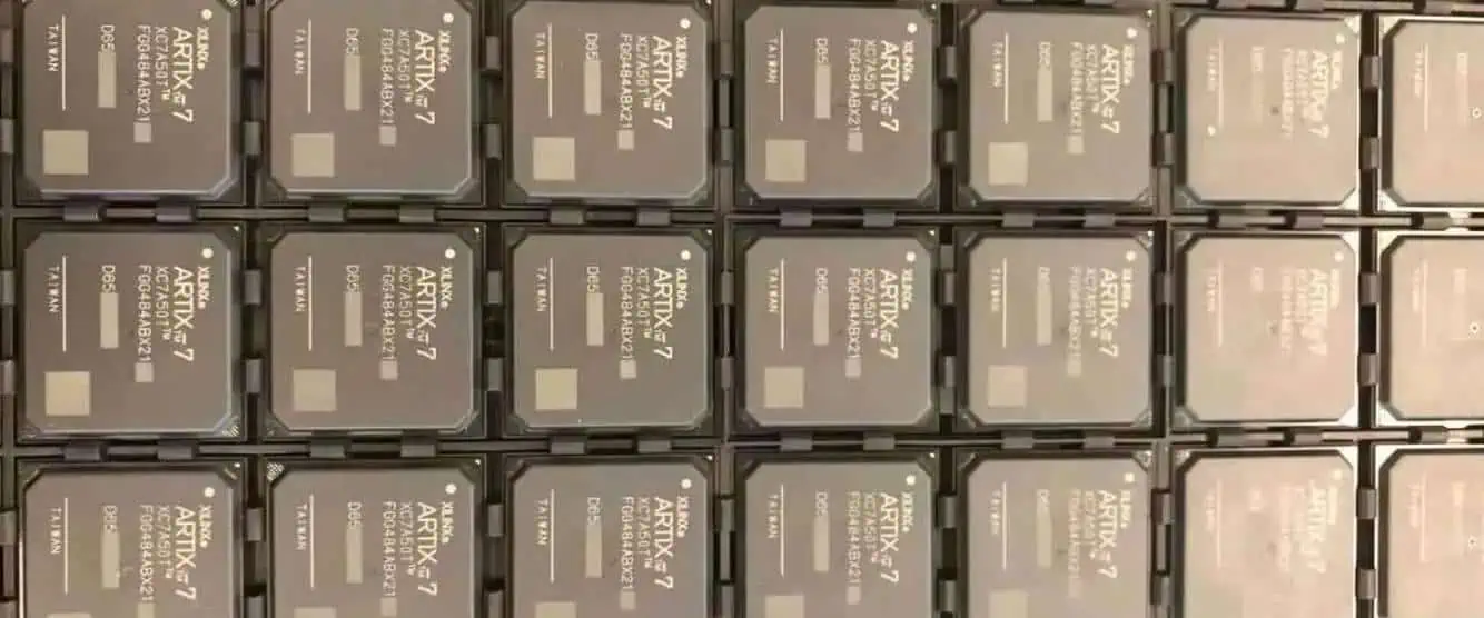
Xilinx FPGA Architecture and Advantages

Xilinx FPGAs offer several architectural advantages that make them compelling platforms for cryptocurrency mining acceleration:

Reconfigurable Logic Fabric

The fundamental strength of Xilinx FPGAs lies in their reconfigurable logic fabric, consisting of configurable logic blocks (CLBs), digital signal processing (DSP) slices, and block RAM (BRAM) resources. This architecture allows for the implementation of custom datapaths optimized specifically for the computational requirements of mining algorithms.

High-Bandwidth Memory Interfaces

Modern Xilinx FPGAs, particularly those in the Ultrascale+ family, support high-bandwidth memory (HBM) and DDR4 interfaces capable of delivering the memory bandwidth required for efficient Ethash computation. The ability to implement custom memory controllers enables optimization of memory access patterns for maximum throughput.

Parallel Processing Capabilities

The inherently parallel nature of FPGA architecture allows for the implementation of multiple independent mining cores on a single device. This parallelism can be exploited at multiple levels, from individual hash function implementations to complete mining pipeline parallelization.

Power Efficiency

When properly optimized, FPGA implementations can achieve superior power efficiency compared to GPU-based mining solutions, particularly important given the energy-intensive nature of cryptocurrency mining operations.

System Architecture Design

xilinx-spartan-6-fpga-tutorial

High-Level System Overview

A comprehensive Xilinx FPGA-based Ethereum mining acceleration system consists of several interconnected components:

Host Interface Layer: Manages communication between the FPGA and host system, typically implemented through PCIe interfaces. This layer handles work distribution, result collection, and system configuration.

Work Distribution Engine: Coordinates the distribution of mining work packages across multiple parallel mining cores, ensuring optimal utilization of available computational resources.

Mining Core Array: The heart of the acceleration system, consisting of multiple parallel Ethash computation engines, each capable of independent operation.

Memory Subsystem: Implements high-performance memory controllers and manages the storage and access of the large DAG dataset required for Ethash computation.

Result Processing Pipeline: Handles the verification and formatting of mining results before transmission back to the host system.

Memory Subsystem Design

The memory subsystem represents one of the most critical components of an FPGA-based Ethash mining system. The DAG dataset, which can exceed 4GB in size, must be stored in external memory and accessed with high bandwidth to maintain computational throughput.

Effective memory subsystem design typically employs:

Multi-Port Memory Controllers: Implementation of multiple independent memory controllers to maximize aggregate bandwidth and reduce access conflicts between parallel mining cores.

Intelligent Caching Strategies: Given the pseudorandom nature of DAG accesses in Ethash, sophisticated caching mechanisms can significantly improve effective memory bandwidth utilization.

Memory Access Optimization: Custom memory access scheduling algorithms that account for the specific access patterns of the Ethash algorithm to minimize latency and maximize throughput.

Mining Core Implementation

Each mining core represents a self-contained Ethash computation engine optimized for FPGA implementation. The core design typically includes:

Keccak-256 Hash Units: Highly optimized implementations of the SHA-3 Keccak hash function, often utilizing dedicated DSP resources for maximum performance.

DAG Access Logic: Specialized circuitry for managing the complex memory access patterns required by the Ethash algorithm.

Nonce Management: Efficient nonce generation and tracking mechanisms to ensure comprehensive search space coverage.

Result Validation: On-chip verification of mining results to reduce unnecessary data transfers to the host system.

Performance Optimization Strategies

Pipeline Optimization

Effective FPGA mining implementations rely heavily on deep pipeline architectures to maximize throughput. Key optimization strategies include:

Computational Pipeline Balancing: Careful analysis and balancing of pipeline stages to eliminate bottlenecks and ensure maximum clock frequency operation.

Memory Access Pipelining: Implementation of sophisticated memory access pipelines that can sustain multiple concurrent DAG lookups while maintaining data coherency.

Result Processing Overlap: Overlapping result processing operations with ongoing computation to minimize idle time and maximize effective utilization.

Resource Utilization Optimization

Xilinx FPGAs offer diverse computational resources that must be carefully allocated for optimal performance:

DSP Slice Utilization: Strategic use of dedicated DSP slices for performance-critical arithmetic operations within the hash computation pipeline.

BRAM Resource Management: Efficient utilization of on-chip block RAM resources for high-frequency data storage and intermediate result buffering.

Logic Resource Optimization: Careful design to maximize the number of parallel mining cores that can be implemented within the available logic resources.

Clock Domain Management

Complex FPGA mining systems often require multiple clock domains to optimize different subsystem operations:

Memory Interface Clocking: Optimization of memory controller clock frequencies to match external memory device specifications and maximize bandwidth.

Computational Core Clocking: Independent optimization of mining core clock frequencies based on critical path analysis and thermal constraints.

Interface Clock Management: Proper management of interface clocks for PCIe and other communication protocols to ensure reliable operation.

Challenges and Implementation Considerations

Thermal Management

FPGA-based mining systems generate significant heat, particularly when operating at maximum performance levels. Effective thermal management strategies include:

Dynamic Voltage and Frequency Scaling: Implementation of adaptive power management techniques that adjust operating parameters based on thermal feedback.

Workload Balancing: Intelligent distribution of computational workload to prevent thermal hotspots and ensure uniform heat distribution across the device.

Cooling System Integration: Design considerations for integration with advanced cooling solutions, including liquid cooling systems for high-performance implementations.

Development Complexity

FPGA-based mining system development presents significant technical challenges:

Algorithm Implementation Complexity: The complexity of implementing optimized Ethash computation engines in hardware description languages requires specialized expertise.

Verification and Validation: Comprehensive testing and validation of complex parallel systems to ensure correctness and reliability under all operating conditions.

Tool Chain Optimization: Effective utilization of Xilinx development tools and optimization flows to achieve optimal implementation results.

Economic Considerations

The viability of FPGA-based mining systems depends on several economic factors:

Development Costs: Significant upfront investment in development time and expertise required to create competitive implementations.

Hardware Costs: FPGA devices, particularly high-end models suitable for mining applications, represent substantial capital investments.

Performance Scalability: The ability to scale performance through parallel device deployment while maintaining economic viability.

Future Implications and Technological Legacy

While Ethereum’s transition to Proof of Stake ended the era of traditional mining on this network, the technological innovations developed for FPGA-based mining systems continue to have broader implications:

Alternative Cryptocurrency Mining

Many other cryptocurrencies continue to utilize proof-of-work consensus mechanisms, creating ongoing opportunities for FPGA-based mining acceleration. The flexible nature of FPGA implementations allows for adaptation to different algorithms with relatively modest development effort.

Computational Acceleration Applications

The optimization techniques and architectural innovations developed for mining applications have found broader applications in high-performance computing, financial modeling, and machine learning acceleration.

Educational and Research Value

FPGA-based mining systems serve as excellent educational platforms for understanding hardware acceleration, parallel computing architectures, and the intersection of computer architecture with economic incentive systems.

Conclusion

Xilinx FPGA-based Ethereum mining acceleration systems represented a sophisticated intersection of reconfigurable computing technology and cryptocurrency economics. These systems demonstrated the potential for FPGA technology to deliver high-performance, power-efficient solutions for computationally intensive applications while highlighting the complex design challenges inherent in developing such systems.

The technical innovations developed during this period continue to influence modern approaches to hardware acceleration and demonstrate the ongoing relevance of FPGA technology in addressing emerging computational challenges. As the cryptocurrency landscape continues to evolve, the fundamental principles and optimization strategies developed for these systems remain valuable for understanding the broader potential of reconfigurable computing in high-performance applications.

The legacy of FPGA-based mining systems extends beyond their original application, contributing to the broader understanding of hardware acceleration, parallel processing architectures, and the economic factors that drive technological innovation in emerging computing domains.

How to Type on LCD Using Bluetooth: Complete Guide

Introduction

In today’s interconnected world, the ability to input text efficiently on devices with LCD displays has become increasingly important. Whether you’re working with a tablet, smartphone, smart TV, or other LCD-equipped device, Bluetooth connectivity offers a wireless solution for text input that can dramatically improve your productivity and user experience. This comprehensive guide will walk you through everything you need to know about typing on LCD displays using Bluetooth technology.

YouTube video

Understanding the Technology

What is Bluetooth?

Bluetooth is a short-range wireless communication technology that allows devices to connect and exchange data without cables. Operating in the 2.4 GHz frequency band, Bluetooth creates a personal area network (PAN) that typically extends up to 30 feet. For typing applications, Bluetooth provides a reliable, low-latency connection between input devices like keyboards and output devices with LCD displays.

LCD Display Integration

LCD (Liquid Crystal Display) technology is found in countless devices today, from smartphones and tablets to laptops, smart TVs, and even refrigerators. When these devices support Bluetooth connectivity, they can receive input from external keyboards, mice, and other peripherals, transforming how we interact with these displays.

Device Compatibility and Setup

Smartphones and Tablets

Most modern smartphones and tablets support Bluetooth keyboard connectivity, making them excellent candidates for enhanced text input.

Android Devices:

  1. Navigate to Settings > Bluetooth
  2. Ensure Bluetooth is enabled
  3. Put your Bluetooth keyboard in pairing mode
  4. Select “Pair new device” or “Add device”
  5. Choose your keyboard from the list of available devices
  6. Enter any required pairing code if prompted

iOS Devices:

  1. Open Settings > Bluetooth
  2. Toggle Bluetooth on if it’s not already active
  3. Set your keyboard to discoverable mode
  4. Tap your keyboard name when it appears in “Other Devices”
  5. Complete any additional pairing steps as prompted

Smart TVs and Streaming Devices

Many smart TVs and streaming devices now support Bluetooth keyboards, making it easier to search for content, enter passwords, and navigate interfaces.

General Setup Process:

  1. Access your TV’s settings menu using the remote
  2. Navigate to Network or Bluetooth settings
  3. Enable Bluetooth if it’s not already active
  4. Put your keyboard in pairing mode
  5. Select “Add Device” or “Search for Devices”
  6. Choose your keyboard and complete the pairing process

Laptops and Computers

While laptops typically have built-in keyboards, Bluetooth connectivity allows for external keyboard use, which can be particularly useful for ergonomic setups or when using the laptop as a desktop replacement.

Windows Setup:

  1. Click the Start button and select Settings
  2. Choose Devices > Bluetooth & other devices
  3. Click “Add Bluetooth or other device”
  4. Select Bluetooth and choose your keyboard
  5. Follow the on-screen instructions to complete pairing

macOS Setup:

  1. Open System Preferences > Bluetooth
  2. Ensure Bluetooth is turned on
  3. Put your keyboard in discoverable mode
  4. Click “Connect” when your keyboard appears
  5. Enter any required pairing code

Types of Bluetooth Input Devices

Physical Keyboards

Physical Bluetooth keyboards offer the most familiar typing experience and come in various form factors:

Full-Size Keyboards: Provide all standard keys including number pad, function keys, and arrow keys. Ideal for productivity work and extended typing sessions.

Compact Keyboards: Smaller footprint while maintaining most functionality. Perfect for travel and limited desk space.

Foldable Keyboards: Ultra-portable options that fold for easy transport. Great for mobile professionals and frequent travelers.

Gaming Keyboards: Feature backlit keys, programmable functions, and enhanced durability for gaming applications.

Virtual and Alternative Input Methods

On-Screen Keyboards: Many devices display virtual keyboards on their LCD screens when text input is required. While not technically Bluetooth-based, these often work in conjunction with Bluetooth mice for point-and-click typing.

Voice Input: Some devices support Bluetooth headsets for voice-to-text input, providing hands-free typing alternatives.

Stylus Input: Bluetooth-enabled styluses can provide handwriting recognition and text input on compatible LCD displays.

Optimizing Your Typing Experience

Keyboard Settings and Customization

Once connected, most operating systems allow you to customize your Bluetooth keyboard experience:

Key Mapping: Assign specific functions to function keys or create custom shortcuts for frequently used commands.

Input Languages: Configure multiple keyboard languages for multilingual typing support.

Auto-Correction: Enable or disable autocorrect features based on your preferences and use case.

Key Repeat Rates: Adjust how quickly keys repeat when held down to match your typing style.

Battery Management

Bluetooth keyboards require power management to ensure consistent performance:

Battery Monitoring: Regularly check battery levels and keep spare batteries or charging cables available.

Power Saving Features: Utilize sleep modes and auto-shutoff features to extend battery life.

Charging Habits: For rechargeable keyboards, maintain good charging practices to preserve battery longevity.

Troubleshooting Common Issues

Connection Problems

Intermittent Disconnections:

  • Check battery levels in your keyboard
  • Ensure devices are within optimal range (typically 30 feet or less)
  • Remove interference from other wireless devices
  • Clear Bluetooth cache on your device if available

Pairing Failures:

  • Reset your keyboard by turning it off and on
  • Clear previous pairing data from both devices
  • Ensure keyboard is in discoverable mode during pairing
  • Try pairing with devices closer together

Input Lag or Delay:

  • Check for interference from other 2.4 GHz devices
  • Ensure both devices have adequate battery power
  • Close unnecessary background applications that might be consuming system resources
  • Consider updating device drivers or firmware

Performance Issues

Missed Keystrokes:

  • Clean keyboard contacts and check for physical damage
  • Verify keyboard is properly paired and connected
  • Check for driver updates for your specific keyboard model
  • Test keyboard with different devices to isolate the issue

Incorrect Character Input:

  • Verify keyboard language settings match your region
  • Check for stuck modifier keys (Shift, Ctrl, Alt)
  • Ensure keyboard layout is correctly configured in device settings
  • Reset keyboard to factory defaults if problems persist

Advanced Features and Applications

Multi-Device Connectivity

Many modern Bluetooth keyboards support connection to multiple devices simultaneously:

Device Switching: Use dedicated keys or key combinations to switch between connected devices quickly.

Profile Management: Maintain separate settings and preferences for different connected devices.

Seamless Workflow: Work across multiple devices without reconnecting or reconfiguring your keyboard.

Specialized Applications

Presentation Control: Use Bluetooth keyboards to control presentations on LCD displays during meetings or conferences.

Media Center Control: Navigate streaming services and media libraries using keyboard shortcuts and navigation keys.

Gaming Integration: Utilize gaming keyboards with LCD-equipped gaming systems for enhanced control and customization.

Home Automation: Control smart home devices with LCD interfaces using Bluetooth keyboards for quick command input.

Security Considerations

Bluetooth Security

When using Bluetooth keyboards with LCD devices, consider these security aspects:

Encryption: Ensure your devices support and use Bluetooth encryption protocols to protect transmitted data.

Authentication: Use devices that require authentication codes during pairing to prevent unauthorized connections.

Range Awareness: Be mindful of your Bluetooth range and potential eavesdropping in public spaces.

Regular Updates: Keep device firmware and drivers updated to address security vulnerabilities.

Future Trends and Developments

Emerging Technologies

Bluetooth 5.0 and Beyond: Newer Bluetooth versions offer improved range, speed, and energy efficiency for better typing experiences.

AI Integration: Smart keyboards with AI features can learn typing patterns and provide predictive text input.

Haptic Feedback: Advanced keyboards may incorporate haptic feedback to simulate physical key presses on flat surfaces.

Gesture Recognition: Future input devices may combine traditional typing with gesture-based controls for enhanced interaction.

Evolving Use Cases

Augmented Reality: As AR displays become more common, Bluetooth input devices will play crucial roles in text input for virtual interfaces.

IoT Integration: Smart keyboards may integrate with Internet of Things ecosystems for enhanced device control and automation.

Accessibility Improvements: Continued development of specialized input devices will improve accessibility for users with various physical limitations.

Conclusion

Typing on LCD displays using Bluetooth technology has revolutionized how we interact with our devices, offering flexibility, convenience, and improved productivity. From basic smartphone text entry to complex multi-device workflows, Bluetooth keyboards provide reliable, wireless solutions for virtually any text input need.

Success with Bluetooth typing depends on proper setup, understanding your device capabilities, and implementing best practices for connection management and troubleshooting. As technology continues to evolve, we can expect even more seamless integration between Bluetooth input devices and LCD displays, opening new possibilities for productivity, entertainment, and creative expression.

Whether you’re a mobile professional, content creator, or casual user, mastering Bluetooth typing techniques will enhance your digital experience and make text input more efficient across all your LCD-equipped devices. Take time to explore the features and customization options available with your specific devices and keyboards to create the optimal typing environment for your needs.

Industrial Motor Control PCBA Design: Integrating Relay Protection, MCU Logic, and Power Management

Introduction

In today’s rapidly evolving industrial automation landscape, the demand for reliable, efficient, and intelligent motor control systems has never been greater. At the heart of these systems lies a critical component: the Motor Control & Protection PCBA (Printed Circuit Board Assembly). This sophisticated electronic module serves as the brain and brawn of industrial motor drives, seamlessly integrating microcontroller logic, relay switching capabilities, robust power management, and comprehensive diagnostic interfaces.

The design and implementation of such a PCBA represents a convergence of multiple engineering disciplines, requiring careful consideration of power electronics, embedded systems design, signal integrity, and industrial safety standards. This article explores the comprehensive design approach for a motor control and protection PCBA that addresses the demanding requirements of modern industrial environments while maintaining the reliability and serviceability essential for mission-critical applications.

YouTube video

System Requirements and Design Objectives

The foundation of any successful motor control PCBA begins with a clear understanding of the operational requirements and environmental constraints it must satisfy. Industrial motor control applications present unique challenges that distinguish them from consumer electronics or even commercial automation systems.

Environmental Robustness: Industrial environments expose electronic systems to extreme temperatures, electromagnetic interference (EMI), mechanical vibrations, and potential exposure to dust, moisture, and corrosive substances. The PCBA must operate reliably across a wide temperature range, typically from -40ยฐC to +85ยฐC, while maintaining performance in the presence of significant electrical noise from variable frequency drives, contactors, and other industrial equipment.

Safety and Compliance: Motor control systems often handle high voltages and currents, making safety paramount. The design must comply with relevant industrial standards such as IEC 61508 for functional safety, UL 508A for industrial control panels, and CE marking requirements for European markets. Galvanic isolation between control logic and power switching circuits is not merely recommended but mandatory for ensuring operator safety and system reliability.

Reliability and Availability: Industrial processes cannot afford unexpected downtime. The PCBA must demonstrate exceptional reliability, with Mean Time Between Failures (MTBF) measured in decades rather than years. This requirement drives design decisions toward proven technologies, redundant protection mechanisms, and comprehensive fault detection capabilities.

Core System Architecture and Components

The motor control and protection PCBA employs a modular architecture that separates critical functions while enabling seamless integration and communication between subsystems.

Microcontroller Unit (MCU): The central processing unit serves as the intelligent core of the system, implementing control algorithms, safety interlocks, communication protocols, and diagnostic routines. Modern industrial MCUs typically feature ARM Cortex-M cores optimized for real-time control applications, offering sufficient computational power for complex control loops while maintaining deterministic response times. The MCU interfaces with external sensors, human-machine interfaces (HMI), and communication networks, enabling both local autonomous operation and integration into larger automation systems.

Relay Control Module: The relay subsystem provides galvanically isolated switching of high-power loads, typically handling currents from several amperes to hundreds of amperes depending on the application. The relay selection process considers factors such as contact rating, switching speed, mechanical life expectancy, and coil power consumption. Driver circuitry ensures proper relay actuation while protecting the MCU from back-EMF and inductive transients generated during switching operations.

Power Management Subsystem: Clean, stable power supplies form the foundation of reliable operation. The power management section typically includes multiple DC/DC converters generating various voltage rails required by different subsystems. For example, +24V for relay coils, +5V and +3.3V for digital logic, and potentially ยฑ12V for analog signal conditioning. Each power rail incorporates appropriate filtering, regulation, and protection to ensure stable operation under varying load conditions.

Interface and Connectivity: Modern industrial systems require extensive connectivity options. The PCBA incorporates multiple interface types including isolated digital inputs/outputs, analog signal conditioning circuits, communication ports (RS485, CAN, Ethernet), and diagnostic connectors. Terminal blocks, pin headers, and industrial connectors provide robust mechanical and electrical connections suitable for industrial wiring practices.

Circuit Design Principles and Implementation

The circuit design philosophy emphasizes reliability, maintainability, and electromagnetic compatibility while optimizing for cost-effectiveness and manufacturing efficiency.

Power Distribution and Filtering: The power input stage implements comprehensive filtering using a combination of common-mode and differential-mode inductors, X and Y capacitors, and metal oxide varistors (MOVs) for surge protection. This multi-stage approach attenuates both conducted and radiated electromagnetic interference while protecting sensitive components from transient overvoltages common in industrial environments.

Ground Plane Strategy: Proper grounding represents one of the most critical aspects of industrial PCB design. The layout employs separate analog and digital ground planes connected at a single star point, minimizing ground loops and reducing noise coupling between high-current switching circuits and sensitive analog signals. Guard rings around critical analog components provide additional isolation from digital switching noise.

Component Selection and Derating: Industrial applications demand conservative component selection with appropriate derating factors. Electrolytic capacitors are typically derated to 50% of their voltage rating, while power semiconductors operate well below their maximum current and thermal limits. This approach significantly enhances long-term reliability at the cost of slightly increased component size and cost.

Thermal Management: Heat dissipation considerations influence both component placement and PCB stackup design. High-power components such as relay drivers, power supply regulators, and protection devices are positioned to facilitate heat spreading through copper pours and thermal vias. The PCB stackup incorporates dedicated thermal layers where necessary to conduct heat away from critical components.

Safety Features and Protection Mechanisms

Industrial motor control systems must incorporate multiple layers of protection to ensure safe operation under both normal and fault conditions.

Overcurrent Protection: Multiple levels of overcurrent protection safeguard both the PCBA and connected loads. Primary protection typically employs fast-acting fuses or circuit breakers sized appropriately for the maximum expected load current. Secondary protection may include electronic current limiting within power supply circuits and software-based overcurrent detection with programmable trip points.

Overvoltage and Surge Protection: Transient voltage suppression (TVS) diodes protect sensitive semiconductor devices from voltage spikes, while MOVs provide coarse protection against larger surge events. The protection scheme considers both common-mode and differential-mode transients, with coordination between protection devices ensuring that lower-energy transients are handled by TVS diodes while MOVs address more severe events.

Thermal Protection: Temperature monitoring occurs at multiple points within the system. Thermal sensors monitor ambient temperature, power dissipation areas, and critical components. The MCU implements temperature-based derating algorithms that reduce performance before reaching damage thresholds, while ultimate protection relies on thermal switches or fuses that disconnect power under extreme conditions.

Galvanic Isolation: Isolation barriers separate control logic from high-voltage switching circuits using optocouplers, magnetic coupling, or capacitive isolation techniques. This isolation not only enhances safety but also improves noise immunity and reduces ground loop susceptibility.

User Interface and Diagnostic Capabilities

Effective field service and troubleshooting require comprehensive diagnostic capabilities and intuitive user interfaces.

Visual Indicators: LED status indicators provide immediate visual feedback on system operating conditions. A typical arrangement includes power-on indicators for each voltage rail, relay status indicators, communication activity lights, and fault condition warnings. Color coding follows industrial conventions: green for normal operation, amber for warnings, and red for fault conditions requiring immediate attention.

Configuration Interface: DIP switches or rotary switches enable field configuration of operating parameters such as communication addresses, input/output assignments, and protection settings. This hardware-based approach ensures that critical settings remain intact even during firmware updates or power cycling.

Test Points and Monitoring: Strategic placement of test points enables field technicians to verify voltages, signal levels, and timing relationships using standard test equipment. These access points are clearly labeled and positioned for safe measurement without requiring removal of covers or disconnection of field wiring.

Diagnostic Communication: The MCU implements comprehensive diagnostic reporting through standard industrial communication protocols. Diagnostic information includes real-time operating parameters, historical fault logs, component health monitoring, and predictive maintenance indicators based on operating hours and environmental conditions.

Applications and Market Integration

The motor control and protection PCBA addresses diverse industrial applications, each with specific requirements and operating characteristics.

Industrial Motor Drives: Integration with variable frequency drives (VFDs) requires coordination between the PCBA’s protection functions and the drive’s internal protection systems. The PCBA typically handles emergency stop functions, external interlock monitoring, and coordination with upstream protective devices while the VFD manages motor-specific protections such as phase loss detection and thermal modeling.

Building Automation Systems: HVAC applications demand integration with building management systems (BMS) through standard protocols such as BACnet or Modbus. The PCBA must interface with various sensors including temperature, pressure, and flow measurement devices while providing coordinated control of pumps, fans, and damper actuators.

Process Automation: Chemical and manufacturing processes require precise coordination between multiple motor-driven devices such as conveyors, mixers, and pumps. The PCBA must support complex sequencing operations, coordinate with safety systems, and maintain operation during communication network disruptions.

Smart Factory Integration: Industry 4.0 initiatives require enhanced connectivity and data analytics capabilities. The PCBA incorporates modern communication interfaces supporting Industrial Ethernet protocols, wireless connectivity options, and edge computing capabilities for local data processing and decision making.

Design Optimization and Manufacturing Considerations

Successful commercial deployment requires careful attention to manufacturing processes, cost optimization, and long-term serviceability.

Design for Manufacturing (DFM): PCB layout optimization considers manufacturing constraints such as minimum trace widths, via sizes, and component spacing requirements. The design accommodates standard assembly processes including surface-mount technology (SMT) placement, wave soldering for through-hole components, and automated optical inspection (AOI) verification.

Supply Chain Management: Component selection considers long-term availability, second-source options, and supply chain stability. Industrial products typically require availability guarantees of 10-15 years, driving selection toward components with demonstrated longevity and broad manufacturer support.

Cost Optimization: Value engineering analyzes the cost-performance relationship for each design element. While industrial applications justify premium components where reliability is paramount, cost optimization focuses on eliminating unnecessary features and selecting components that meet requirements without excessive over-specification.

Serviceability: Modular design facilitates field replacement of major subsystems without requiring specialized tools or extensive disassembly. Components most likely to require replacement, such as relays and fuses, are positioned for easy access and clearly identified for field personnel.

Conclusion

The design of industrial motor control and protection PCBAs represents a sophisticated integration of multiple engineering disciplines, balancing competing requirements for reliability, cost-effectiveness, and functionality. Success depends on thorough understanding of application requirements, careful selection and integration of components, and meticulous attention to safety and regulatory compliance.

As industrial automation continues to evolve toward greater connectivity, intelligence, and efficiency, motor control PCBAs will increasingly serve as critical enablers of smart manufacturing and Industry 4.0 initiatives. The design principles and implementation strategies outlined in this article provide a foundation for developing robust, reliable motor control solutions that meet the demanding requirements of modern industrial applications while positioning for future technological advancement.

The integration of advanced MCU capabilities, robust protection mechanisms, and comprehensive diagnostic features creates a platform capable of supporting both current operational requirements and future enhancement through firmware updates and modular expansion. This forward-looking approach ensures that investment in motor control infrastructure continues to provide value throughout the extended lifecycle typical of industrial automation systems.

How to Start with PCB Design: Essential Concepts for Beginners

Printed Circuit Board (PCB) design is a fascinating blend of electrical engineering, mechanical design, and manufacturing knowledge that forms the backbone of modern electronics. Whether you’re an electronics hobbyist, engineering student, or professional looking to expand your skillset, understanding PCB design opens up a world of possibilities for creating custom electronic devices. This comprehensive guide will walk you through the essential concepts and provide a roadmap for beginning your PCB design journey.

YouTube video

What is PCB Design?

A Printed Circuit Board is a flat board made of insulating material, typically fiberglass (FR4), with conductive copper traces that connect electronic components together. PCB design is the process of creating the layout for these boards, determining where components will be placed and how they will be electrically connected. Unlike breadboards or perfboards used for prototyping, PCBs provide a permanent, reliable, and compact solution for electronic circuits.

The PCB serves multiple functions: it provides mechanical support for components, creates electrical connections between them, and can include additional features like heat dissipation, electromagnetic shielding, and signal integrity management. Modern PCBs can have multiple layers, with complex routing and advanced features that enable the compact, high-performance devices we use daily.

Fundamental PCB Concepts

Board Layers and Stack-up

PCBs can have anywhere from one to dozens of layers, though most beginners will work with two or four-layer boards. A typical two-layer board has components and traces on the top layer (component side) and additional traces on the bottom layer (solder side). Four-layer boards add dedicated power and ground planes between the outer layers, providing better power distribution and signal integrity.

The layer stack-up refers to the arrangement of these conductive and insulating layers. Understanding stack-up is crucial because it affects signal integrity, power distribution, manufacturing cost, and board thickness. Each additional layer increases complexity and cost but provides more routing space and better electrical performance.

Components and Footprints

Every electronic component that goes on a PCB needs a corresponding footprint โ€“ a pattern of copper pads that matches the component’s physical connections. Footprints must precisely match the component’s dimensions, pin spacing, and mounting requirements. Common component packages include through-hole (components with leads that go through the board) and surface-mount (components that sit on the board surface).

Understanding component packages is essential because they determine board density, manufacturing requirements, and assembly processes. Surface-mount components allow for much higher density but require more sophisticated manufacturing and assembly equipment. Through-hole components are easier to hand-solder but take up more space.

Traces, Vias, and Routing

Traces are the copper paths that carry electrical signals between components. They’re essentially wires printed on the board surface. The width of traces depends on the current they need to carry โ€“ power traces are typically wider than signal traces. Trace routing requires careful planning to minimize interference and ensure all connections are made efficiently.

Vias are plated holes that allow electrical connections between different layers of the board. They enable complex routing by allowing traces to change layers when needed. There are different types of vias: through-hole vias go through the entire board, blind vias connect outer layers to inner layers, and buried vias connect only inner layers.

The PCB Design Process

Schematic Design

Every PCB starts with a schematic โ€“ a symbolic representation of the electrical connections in your circuit. The schematic shows which components are connected and how they interact, but it doesn’t indicate physical placement or routing. This step is crucial because errors in the schematic will carry through to the PCB design.

A good schematic is clear, well-organized, and includes all necessary information for PCB layout. It should specify component values, reference designators, and any special requirements. Many PCB design tools can automatically generate a netlist from the schematic, which defines all the electrical connections needed in the PCB layout.

Component Placement

Once the schematic is complete, the next step is placing components on the PCB. Good component placement is critical for successful routing, thermal management, and manufacturing. Components should be grouped logically, with related circuits placed close together to minimize trace lengths and reduce noise.

Consider the physical constraints during placement: components need adequate clearance for assembly, heat-generating components should have good thermal paths, and mechanical connectors must align with enclosure requirements. High-speed signals benefit from short, direct paths, while sensitive analog circuits should be isolated from noisy digital sections.

Routing

Routing involves creating the actual copper traces that connect the components according to the schematic. This is often the most time-consuming part of PCB design, especially for complex boards. Modern PCB design software includes auto-routers, but manual routing often produces better results, especially for critical signals.

Good routing practices include keeping traces as short as possible, avoiding sharp angles, maintaining consistent trace widths for similar signals, and providing adequate spacing between traces to prevent interference. Power and ground connections typically use wider traces or dedicated planes to handle higher currents and provide good power distribution.

Essential Tools and Software

PCB Design Software

Several PCB design tools are available, ranging from free options suitable for beginners to professional-grade software used in industry. KiCad is an excellent free, open-source option that provides professional features without cost restrictions. It includes schematic capture, PCB layout, and a 3D viewer for design visualization.

For commercial options, Altium Designer is widely used in professional settings, while Eagle (now part of Autodesk Fusion 360) offers a good balance of features and affordability. Cloud-based tools like EasyEDA provide accessibility and collaboration features. Choose software that matches your budget, feature requirements, and learning preferences.

Component Libraries

Accurate component libraries are essential for successful PCB design. These libraries contain the schematic symbols and PCB footprints for electronic components. Many design tools come with extensive built-in libraries, but you’ll often need to create custom components or find additional libraries from component manufacturers.

Always verify footprints against component datasheets, as incorrect footprints can render a board unusable. Many component manufacturers provide PCB libraries for their parts, which can save significant time and reduce errors.

Design Rules and Best Practices

PCB Antenna Layout
PCB Antenna Layout

Electrical Design Rules

PCB design involves numerous rules that ensure the board will function correctly and can be manufactured reliably. Minimum trace width depends on current requirements and manufacturing capabilities. Typical minimum trace widths for standard PCB processes range from 0.1mm to 0.15mm, though wider traces are often used for better reliability and current handling.

Via sizes also have minimum requirements, typically 0.2mm or larger for standard processes. Spacing between traces, vias, and pads must meet manufacturing tolerances, usually 0.1mm or greater. These rules prevent manufacturing defects and ensure reliable electrical connections.

Signal Integrity Considerations

As signals become faster or more sensitive, signal integrity becomes increasingly important. This involves managing signal timing, reducing noise, and preventing interference between circuits. Good practices include using ground planes for signal return paths, keeping high-speed traces short and direct, and avoiding routing sensitive signals near noisy circuits.

Impedance control becomes important for high-speed signals, requiring specific trace geometries and dielectric properties. While beginners may not encounter these requirements immediately, understanding these concepts prepares you for more advanced designs.

Common Beginner Mistakes

Inadequate Planning

One of the most common mistakes is jumping into PCB layout without sufficient planning. Proper component placement and routing strategy planning can save hours of work later. Consider the overall signal flow, mechanical constraints, and manufacturing requirements before starting detailed routing.

Ignoring Manufacturing Constraints

Every PCB manufacturer has specific capabilities and limitations. Design rules like minimum trace width, via sizes, and spacing requirements must be followed to ensure your board can be manufactured correctly. Always check with your chosen manufacturer’s specifications before finalizing your design.

Poor Power and Ground Distribution

Inadequate power and ground distribution can cause numerous problems, from component malfunction to electromagnetic interference. Ensure power traces can handle the required current, and provide solid ground connections for all components. Ground loops and poor grounding can cause significant noise and reliability issues.

Getting Started: Your First PCB Project

Choose a Simple Project

Start with a simple project that matches your current skill level. A basic LED circuit, simple sensor board, or breakout board for a specific component makes an excellent first project. These projects teach fundamental concepts without overwhelming complexity.

Follow a Tutorial

Many online tutorials walk through complete PCB design projects step-by-step. Following a detailed tutorial helps you learn the software tools while creating a functional board. This approach provides hands-on experience with all aspects of the design process.

Design for Learning

Your first PCB doesn’t need to be perfect or revolutionary. Focus on learning the process, understanding the tools, and gaining experience with design concepts. Make deliberate choices about complexity โ€“ it’s better to complete a simple design successfully than to struggle with an overly ambitious first project.

Manufacturing and Assembly Considerations

PCB Fabrication

Understanding PCB manufacturing helps you design boards that are cost-effective and reliable. Standard PCB processes are well-suited to most beginner projects and offer good performance at reasonable cost. Specify standard materials, layer counts, and feature sizes unless you have specific requirements for advanced capabilities.

Assembly Options

Consider how your PCB will be assembled when designing component placement and selecting components. Hand assembly is feasible for simple boards with larger components, while complex boards with fine-pitch components may require professional assembly services.

Conclusion

PCB design is a rewarding skill that opens up endless possibilities for creating custom electronic devices. While the learning curve can seem steep initially, starting with simple projects and gradually building complexity allows you to develop expertise systematically. Focus on understanding fundamental concepts, practice with real projects, and don’t be afraid to iterate and improve your designs.

The key to success in PCB design is combining theoretical knowledge with practical experience. Start designing simple boards, learn from mistakes, and gradually tackle more complex projects as your skills develop. With patience and practice, you’ll soon be creating professional-quality PCBs for your electronic projects.

Remember that PCB design is both an art and a science, requiring technical knowledge, creativity, and attention to detail. The investment in learning these skills pays dividends in your ability to create reliable, manufacturable electronic devices that bring your ideas to life.

PCB Power Handling: How Board Thickness Prevents Overheating and Failure

power pcb

Modern electronic systems are pushing the boundaries of power density, cramming more functionality into smaller spaces while demanding higher performance. At the heart of these systems lies the printed circuit board (PCB), which must not only provide electrical connectivity but also serve as a critical thermal management component. Understanding how board thickness influences power handling capabilities is essential for preventing catastrophic overheating and ensuring reliable operation across demanding applications.

YouTube video

The Thermal Challenge in Modern PCBs

As electronic devices become more compact and powerful, the heat generated per unit area continues to increase dramatically. Power semiconductor devices, high-frequency processors, and dense component layouts create thermal hotspots that can quickly exceed safe operating temperatures. When a PCB cannot adequately dissipate this heat, components experience reduced performance, shortened lifespan, or complete failure.

The relationship between power handling and board thickness is fundamentally rooted in thermal physics. Heat generated by components must travel through the PCB substrate to reach heat sinks, thermal vias, or the ambient environment. The efficiency of this heat transfer process directly impacts the maximum power that can be safely handled without compromising system reliability.

Understanding Heat Flow in PCB Substrates

Heat transfer in PCBs occurs primarily through conduction, following the basic principle that heat flows from hot regions to cooler ones. The rate of heat transfer depends on several factors: the thermal conductivity of the materials, the cross-sectional area available for heat flow, the temperature gradient, and the distance the heat must travel.

Board thickness plays a crucial role in this equation by affecting both the thermal resistance and the available pathways for heat dissipation. A thicker board provides more material volume to absorb and distribute heat, effectively creating a larger thermal mass that can buffer temperature spikes during transient power events.

The Physics of Thermal Resistance

Thermal resistance in a PCB can be understood using an electrical analogy, where heat flow resembles current flow and temperature differences correspond to voltage drops. The thermal resistance of a material is inversely proportional to its cross-sectional area and directly proportional to its thickness and the reciprocal of its thermal conductivity.

For a uniform material, thermal resistance equals thickness divided by the product of thermal conductivity and cross-sectional area. This relationship initially suggests that increasing thickness would increase thermal resistance, making heat transfer more difficult. However, the reality in PCB applications is more complex due to the multi-layered nature of modern boards and the distribution of heat sources and sinks.

In practice, thicker PCBs often demonstrate better thermal performance because they provide increased copper volume for heat spreading and more space for thermal management features like buried thermal vias, thick copper planes, and thermal interface materials.

Material Considerations and Thermal Properties

The substrate material significantly influences how board thickness affects thermal performance. Standard FR-4 fiberglass has relatively poor thermal conductivity (approximately 0.3 W/mยทK), making it somewhat inefficient for heat conduction. However, thicker FR-4 boards can still improve thermal performance by providing more volume for copper layers and thermal vias.

High-performance applications often utilize substrates with enhanced thermal properties. Materials like aluminum-backed PCBs, ceramic substrates, or specialized thermally-enhanced laminates offer superior thermal conductivity. When combined with increased thickness, these materials can dramatically improve power handling capabilities.

Copper layers within the PCB stack-up play an equally critical role. Copper’s excellent thermal conductivity (approximately 400 W/mยทK) makes it the primary heat spreading mechanism in most PCBs. Thicker boards allow for heavier copper weights and additional copper layers, creating more efficient thermal pathways throughout the board.

Heat Spreading and Distribution Benefits

One of the most significant advantages of increased board thickness is improved heat spreading capability. When a high-power component generates heat, that energy must be distributed across a larger area to prevent localized hot spots. Thicker boards provide more copper volume and additional layers that can act as heat spreaders, distributing thermal energy more evenly across the board’s surface.

This spreading effect is particularly important for power components like voltage regulators, power MOSFETs, and high-current connectors. By distributing heat over a larger area, the local temperature rise is reduced, allowing components to operate within their safe temperature limits even at higher power levels.

Thermal Via Design and Implementation

Thicker PCBs offer enhanced opportunities for thermal via implementation. Thermal vias are copper-filled holes that create vertical heat conduction paths between layers, allowing heat to transfer from hot components to cooler areas of the board or to external heat sinks.

In thicker boards, thermal vias can be larger in diameter and more numerous without compromising structural integrity or routing density. Additionally, the increased board thickness allows for more sophisticated via arrangements, such as via-in-pad designs or arrays of thermal vias that create highly effective heat conduction paths.

The thermal resistance of a via depends on its diameter, length, and the thermal interface between the via and the surrounding materials. Thicker boards, while requiring longer vias, can accommodate larger diameters and better thermal interfaces, often resulting in net improvements in thermal performance.

Design Strategies for Optimal Thermal Performance

fr4 thermal conductivity

Effective thermal management in thicker PCBs requires careful consideration of layer stack-up design. Dedicated thermal layers, typically implemented as solid copper planes, can be strategically positioned throughout the board stack-up to create efficient heat spreading networks. These layers should be connected through thermal vias and designed to minimize thermal bottlenecks.

Component placement becomes increasingly critical in thicker board designs. High-power components should be positioned to take advantage of thermal pathways and avoid creating thermal shadows that could trap heat. The three-dimensional nature of thicker boards allows for more sophisticated thermal routing, including the use of buried heat spreaders and internal thermal interfaces.

Copper balancing across layers also impacts thermal performance. Unbalanced copper distribution can create thermal gradients that lead to warping and mechanical stress. Thicker boards are generally more tolerant of copper imbalances, but careful design is still required to optimize thermal performance.

Trade-offs and Design Considerations

While increased board thickness generally improves thermal performance, it comes with several trade-offs that designers must consider. Thicker boards increase manufacturing costs due to longer processing times, more materials, and potentially lower yields. They also add weight and volume to the final product, which may be critical constraints in portable or aerospace applications.

Manufacturing constraints also become more challenging with increased thickness. Aspect ratios for vias become more demanding, requiring careful consideration of drill sizes and plating processes. Signal integrity can be affected by longer via lengths, potentially requiring additional design measures to maintain electrical performance.

Mechanical considerations include increased stiffness, which can be beneficial for reducing vibration-induced failures but may also increase stress concentrations at component interfaces. The coefficient of thermal expansion mismatch between the PCB and components can also become more pronounced in thicker boards, requiring careful attention to solder joint reliability.

Real-World Applications and Case Studies

High-power LED applications demonstrate the benefits of increased board thickness particularly well. LED arrays generate significant heat in small areas, and failure to manage this heat leads to rapid degradation of light output and color stability. Thick aluminum-backed PCBs or multi-layer boards with heavy copper have become standard solutions for high-performance LED systems.

Power electronics applications, including motor drives, power supplies, and electric vehicle systems, routinely utilize thick PCBs to handle high current densities. These applications often combine thick substrates with specialized thermal interface materials and external heat sinks to achieve optimal thermal performance.

Telecommunications and data center equipment represent another area where thick PCBs provide thermal advantages. High-speed processors and power amplifiers in these systems generate substantial heat loads that require sophisticated thermal management strategies, often including thick multi-layer boards with integrated thermal features.

Future Trends and Emerging Technologies

The trend toward higher power densities and more compact electronic systems continues to drive innovations in PCB thermal management. Advanced materials with enhanced thermal properties, including graphene-enhanced substrates and diamond-like carbon coatings, are being integrated into thicker board designs to push thermal performance boundaries.

Three-dimensional integration technologies are also benefiting from advances in thick board thermal management. As components are stacked vertically and integrated more densely, the ability to conduct heat through thick substrates becomes increasingly critical for system reliability.

Conclusion

Board thickness represents a fundamental design parameter that significantly influences PCB power handling capabilities. While the relationship between thickness and thermal performance is complex and application-dependent, thicker boards generally provide superior thermal management through increased thermal mass, enhanced heat spreading, and improved opportunities for thermal via implementation.

Successful thermal management in high-power PCB applications requires a holistic approach that considers material selection, layer stack-up design, component placement, and manufacturing constraints. As electronic systems continue to demand higher power densities, understanding and leveraging the thermal benefits of increased board thickness will remain essential for preventing overheating and ensuring reliable operation.

The investment in thicker PCB designs often pays dividends in improved reliability, longer component lifespans, and the ability to push system performance boundaries. For engineers working with high-power applications, careful consideration of board thickness as part of a comprehensive thermal management strategy is not just beneficialโ€”it’s essential for success.

5 Key Strategies to Optimize Your PCB Manufacturing Layout

Hardware Layout

Printed circuit board (PCB) design has become increasingly sophisticated and critical to product success. As devices become smaller, faster, and more complex, optimizing your PCB manufacturing layout is essential for achieving reliable performance, cost-effectiveness, and manufacturability. Whether you’re designing consumer electronics, industrial equipment, or cutting-edge IoT devices, implementing strategic layout optimization techniques can mean the difference between a successful product launch and costly redesigns.

Effective PCB layout optimization goes beyond simply fitting components onto a board. It requires a comprehensive understanding of electrical principles, manufacturing constraints, thermal management, and signal integrity considerations. The following five key strategies will help you create PCB layouts that not only meet your functional requirements but also optimize manufacturing efficiency, reduce costs, and improve overall product reliability.

Strategy 1: Design for Manufacturing (DFM) Principles

design for manufacturing

Design for Manufacturing represents the foundation of successful PCB layout optimization. This approach involves making design decisions that simplify the manufacturing process while maintaining product functionality and performance. By considering manufacturing constraints early in the design phase, you can avoid costly revisions and production delays.

The cornerstone of DFM in PCB design is understanding your manufacturer’s capabilities and limitations. Different fabrication houses have varying specifications for minimum trace widths, via sizes, spacing requirements, and layer stackup options. Establishing these parameters before beginning your layout ensures your design will be manufacturable without requiring expensive custom processes or premium pricing.

Trace width and spacing optimization plays a crucial role in DFM implementation. While it might be tempting to use the minimum allowable dimensions to maximize routing density, this approach often leads to manufacturing challenges and reduced yields. Instead, use wider traces and larger spacing wherever possible, reserving minimum dimensions only for areas where space constraints absolutely require them. This approach improves manufacturing reliability and often reduces costs by allowing the use of standard fabrication processes.

Component placement strategy significantly impacts manufacturing efficiency. Grouping components by type and size facilitates automated assembly processes and reduces setup times. Orient components consistently to minimize machine programming complexity and reduce the likelihood of placement errors. Consider the assembly sequence when placing components, ensuring that larger components don’t shadow smaller ones during reflow soldering or wave soldering processes.

Via design and placement require careful consideration for optimal manufacturability. Use standard via sizes whenever possible, as non-standard dimensions require special tooling and increase costs. Minimize the number of different via sizes in your design to reduce manufacturing complexity. Place vias away from component pads to avoid interference during assembly and to prevent solder wicking issues that can lead to poor joints.

Panelization strategy should be considered from the beginning of your layout process. Design your PCB dimensions and shape to optimize panel utilization, reducing waste and lowering per-unit costs. Include appropriate tooling holes, fiducial markers, and handling features that facilitate automated manufacturing processes. Consider how individual boards will be separated from the panel, ensuring that the separation method won’t damage critical circuits or components.

Strategy 2: Signal Integrity and EMI Optimization

Modern electronic devices operate at increasingly high frequencies, making signal integrity and electromagnetic interference (EMI) control critical aspects of PCB layout optimization. Poor signal integrity can lead to timing errors, data corruption, and system failures, while inadequate EMI control can cause regulatory compliance issues and interference with other devices.

Ground plane strategy forms the backbone of effective signal integrity design. Implement continuous ground planes wherever possible, as they provide low-impedance return paths for high-frequency signals and help control EMI. When ground plane splits are unavoidable, ensure that high-speed signals don’t cross these discontinuities, as this can cause signal reflections and increased electromagnetic emissions. Use stitching vias to connect ground planes on different layers, maintaining low impedance paths throughout your stackup.

Controlled impedance routing becomes essential when dealing with high-speed digital signals or sensitive analog circuits. Work with your fabricator to establish appropriate trace geometries for your target impedance values, considering factors such as dielectric constant, trace width, thickness, and the distance to reference planes. Maintain consistent impedance along signal paths by avoiding unnecessary vias, sharp bends, or changes in trace width. For differential pairs, maintain tight coupling and consistent spacing to preserve signal quality.

Power distribution network (PDN) design significantly impacts both signal integrity and EMI performance. Implement a low-impedance power distribution system using dedicated power planes, wide traces, and strategically placed decoupling capacitors. Place decoupling capacitors as close as possible to power pins of active components, with different capacitor values targeting various frequency ranges. Consider the inductance of vias and traces when connecting decoupling capacitors to power and ground planes.

Layer stackup optimization provides the foundation for controlled impedance and EMI management. Work with your fabricator to develop a stackup that supports your impedance requirements while providing adequate power and ground plane coverage. Alternate signal layers with reference planes to provide consistent return paths and minimize crosstalk. Consider using thinner dielectrics for better high-frequency performance, but balance this against manufacturing complexity and cost.

Routing topology and techniques play a crucial role in maintaining signal integrity. Keep high-speed traces as short as possible and avoid unnecessary vias that introduce discontinuities. Route critical signals on inner layers when possible, as they benefit from better shielding and more consistent impedance. Implement proper termination strategies for high-speed signals, using series termination for point-to-point connections and parallel termination for longer lines or multiple loads.

Strategy 3: Thermal Management and Reliability Enhancement

Thermal management has become increasingly critical as component densities increase and power dissipation rises in modern electronic designs. Effective thermal design not only prevents component damage but also improves reliability, extends operating life, and maintains consistent performance across temperature variations.

Heat dissipation pathway design requires careful consideration of thermal flow from heat-generating components to heat sinks or ambient air. Identify components with significant power dissipation and create efficient thermal paths using copper planes, thermal vias, and strategic component placement. Large copper areas act as heat spreaders, distributing thermal energy over a wider area to facilitate cooling. Connect these copper areas to internal planes when possible to increase the thermal mass available for heat absorption.

Thermal via implementation provides crucial vertical heat conduction paths in multilayer PCBs. Place arrays of thermal vias directly beneath high-power components to conduct heat away from the component and into internal copper layers or the opposite side of the board. Use multiple small vias rather than fewer large ones to maximize heat transfer while minimizing impact on routing density. Consider filled vias for applications requiring maximum thermal performance, though this adds manufacturing cost and complexity.

Component placement strategy for thermal management involves distributing heat sources across the board rather than concentrating them in one area. Separate high-power components when possible to prevent hot spots that can lead to thermal runaway or accelerated aging. Place temperature-sensitive components away from heat sources and in areas with good airflow or thermal coupling to heat sinks. Consider the thermal coefficient of critical components when placing them relative to heat sources.

Copper balance and symmetry affect both thermal performance and mechanical reliability. Maintain similar copper distribution on opposite sides of the board to prevent warping during assembly and temperature cycling. Use copper fills in unused areas to improve heat spreading and reduce thermal gradients across the board. However, ensure that these fills don’t create EMI issues or interfere with impedance control requirements.

Solder joint reliability depends heavily on thermal design, as thermal cycling creates mechanical stress in solder joints. Minimize temperature differences between components and the PCB substrate by providing good thermal coupling. Consider the coefficient of thermal expansion mismatch between components and the PCB material, especially for large components or those with different package materials. Implement thermal relief connections for components that need to be soldered to large copper areas, as this prevents the copper from acting as a heat sink during soldering.

Strategy 4: Power Integrity and Distribution Optimization

Power integrity has become as critical as signal integrity in modern PCB design, particularly with the trend toward lower supply voltages and higher current requirements. Poor power distribution can lead to voltage droops, increased noise, and system instability, while optimized power delivery ensures reliable operation across all operating conditions.

Power distribution network architecture requires careful planning to deliver clean, stable power to all components. Implement dedicated power planes for major supply voltages, as these provide low impedance distribution and help reduce power supply noise. For multi-voltage designs, carefully plan power plane splits to minimize the impact on signal return paths while maintaining power integrity for each supply domain. Consider using separate layers for different voltage levels to avoid conflicts and simplify routing.

Decoupling capacitor strategy plays a fundamental role in power integrity optimization. Implement a hierarchical decoupling approach using multiple capacitor values to address different frequency ranges. Large electrolytic or tantalum capacitors handle low-frequency variations and provide bulk charge storage, while smaller ceramic capacitors address high-frequency switching noise. Place high-frequency decoupling capacitors as close as possible to the power pins of active components to minimize loop inductance.

Current density management ensures reliable power delivery without excessive voltage drops or heating. Calculate current requirements for each section of your power distribution network and size traces and planes accordingly. Use current density guidelines appropriate for your application, considering factors such as temperature rise, trace length, and copper thickness. Implement multiple parallel paths for high-current supplies to distribute the current load and improve reliability.

Voltage regulation placement and routing significantly impact power integrity performance. Place voltage regulators close to their load circuits to minimize resistive losses and improve transient response. Route high-current paths using wide traces or copper pours, and avoid routing power supplies through connector pins or narrow sections that could create bottlenecks. Consider the impact of switching regulator layouts on EMI and include appropriate filtering and shielding techniques.

Power supply sequencing and protection features should be considered during the layout phase. Some components require specific power-up sequences or have maximum voltage differential requirements between supplies. Plan your power distribution to support these requirements through proper decoupling, sequencing circuits, and protection components. Include test points for critical power supplies to facilitate debugging and production testing.

Strategy 5: Automation and Advanced Layout Techniques

PCB Layout in KiCA
PCB Layout in KiCA

Modern PCB design tools offer sophisticated automation features that can significantly improve layout quality while reducing design time. Understanding and effectively utilizing these advanced techniques can help you achieve optimal results while maintaining design consistency and meeting complex requirements.

Auto-routing and interactive routing tools have evolved significantly, offering intelligent routing capabilities that consider multiple constraints simultaneously. Modern auto-routers can handle complex rules including impedance control, length matching, and EMI requirements while optimizing routing density and minimizing layer usage. However, successful automation requires careful constraint setup and rule definition. Critical signals often benefit from manual routing or guided auto-routing to ensure optimal performance.

Length matching and timing analysis become crucial in high-speed designs where signal timing directly impacts functionality. Utilize your design tools’ length matching capabilities to equalize trace lengths within specified tolerances for clock distribution, data buses, and differential pairs. Advanced tools can perform timing analysis during the layout process, allowing real-time optimization of critical timing paths. Consider the impact of via delays and trace bends when calculating timing requirements.

Design rule checking (DRC) and constraint management ensure that your layout meets all electrical, mechanical, and manufacturing requirements. Establish comprehensive design rules early in the project, including manufacturing constraints, electrical requirements, and company standards. Use hierarchical constraint systems that allow different rules for different circuit sections or signal classes. Perform regular DRC checks throughout the design process rather than waiting until completion to identify and resolve issues.

3D modeling and mechanical integration capabilities help identify potential mechanical conflicts before manufacturing. Use 3D visualization tools to verify component clearances, connector accessibility, and mechanical fit within enclosures. Consider the impact of component tolerances and PCB warpage on final assembly. Integrate mechanical constraints into your electrical design tools to catch conflicts early in the design process.

Collaboration and version control features become essential for team-based designs or projects requiring multiple iterations. Implement proper version control procedures to track design changes and maintain design history. Use collaborative design features that allow multiple designers to work on different sections simultaneously while maintaining design integrity. Establish clear documentation standards and change control procedures to ensure that all team members understand design requirements and modifications.

Conclusion

Optimizing your PCB manufacturing layout requires a comprehensive approach that balances electrical performance, manufacturing efficiency, thermal management, and design automation. By implementing these five key strategies โ€“ Design for Manufacturing principles, signal integrity optimization, thermal management, power integrity enhancement, and advanced layout techniques โ€“ you can create PCB designs that meet performance requirements while minimizing costs and maximizing reliability.

Success in PCB layout optimization comes from understanding the interdependencies between these various aspects of design. Manufacturing constraints influence electrical performance, thermal considerations affect component placement, and power integrity impacts signal quality. By considering these relationships early in the design process and applying systematic optimization techniques, you can achieve superior results that meet both technical and business objectives.

The investment in proper PCB layout optimization pays dividends throughout the product lifecycle, from reduced development time and manufacturing costs to improved field reliability and customer satisfaction. As electronic systems continue to evolve toward higher performance and greater integration, mastering these optimization strategies becomes increasingly valuable for design success.

Addressing Low-Power Design Challenges in AI Smart Glasses with NXP Processors

The transformation of artificial intelligence from laboratory curiosity to consumer necessity has catalyzed a remarkable evolution in wearable technology. Among the most compelling manifestations of this convergence are AI-powered smart glasses, devices that have transcended their science fiction origins to become sophisticated platforms for human-computer interaction. These innovative wearables represent a paradigm shift in how we access and process information, offering unprecedented convenience through seamless integration of advanced computing capabilities into an unobtrusive form factor.

Today’s AI smart glasses ecosystem encompasses a diverse array of applications that extend far beyond simple augmented reality overlays. Users can leverage these devices for teleprompting during presentations, capturing high-quality photographs with intelligent scene recognition, performing real-time object identification and translation, accessing turn-by-turn navigation without visual distraction, monitoring health metrics continuously, and even conducting contactless payments. This comprehensive functionality positioning makes AI glasses an ideal platform for the next generation of human-machine interaction applications, eliminating the need for users to constantly retrieve and manipulate their smartphones.

The Fundamental Power Challenge

Despite their impressive capabilities, AI smart glasses face a critical engineering challenge that threatens to limit their widespread adoption: power consumption management. The fundamental constraint stems from the inherent conflict between performance requirements and physical limitations. To maintain user comfort and aesthetic appeal, smart glasses must remain lightweight, typically weighing less than 30 grams. This weight restriction severely limits battery capacity, with most devices incorporating batteries ranging from just 200 to 300mAh โ€“ a fraction of what modern smartphones provide.

The power challenge becomes even more complex when considering the computational demands of AI applications. High-performance application processors required for advanced AI functions typically utilize cutting-edge semiconductor process nodes of 6nm and below. While these advanced manufacturing processes deliver exceptional dynamic performance and computational density, they introduce a significant drawback: exponentially increasing leakage current as transistor dimensions shrink.

This leakage current represents power consumption that occurs even when the processor is not actively performing computations, creating a constant drain on the limited battery capacity. The mathematical relationship between process node advancement and leakage current creates a fundamental trade-off where the very technology that enables sophisticated AI capabilities simultaneously undermines the battery life that makes the device practical for everyday use. This conflict between high-performance processing requirements and stringent power budgets has become the defining challenge in AI glasses development.

Architectural Approaches to Power Optimization

The industry has responded to these power challenges by developing two primary architectural approaches, each representing different trade-offs between functionality and efficiency.

The Application Processor Plus Coprocessor Architecture

The first approach employs a dual-processor strategy that separates high-performance computing tasks from always-on functions. This “Application Processor + Coprocessor” architecture enables manufacturers to deliver feature-rich devices without completely sacrificing battery life.

The application processor in this configuration serves as the powerhouse, built using advanced process technology to maximize computational performance. This processor handles demanding tasks including high-resolution image and video processing, complex neural network computations through dedicated Neural Processing Units (NPUs), and high-bandwidth wireless connectivity via Wi-Fi and Bluetooth modules. When active, this processor delivers the computational horsepower necessary for sophisticated AI applications such as real-time object recognition, natural language processing, and augmented reality rendering.

Complementing this high-performance processor is a carefully designed coprocessor that prioritizes efficiency over raw computational power. This secondary processor typically employs more mature semiconductor manufacturing processes that offer better power characteristics for always-on operations. The coprocessor integrates optimized transistor designs, combining long-channel and short-channel devices to achieve superior power efficiency during low-frequency operations and minimize static power consumption.

The coprocessor assumes responsibility for continuous background functions including voice wake-up detection, audio processing for calls and music playback, and basic user interface rendering. Its integrated GPU enables vector graphics processing and text rendering for essential display functions, while a dedicated AI acceleration unit enhances voice recognition accuracy and provides real-time noise reduction capabilities.

The Low-Power Processor Main Control Architecture

The alternative architectural approach prioritizes maximum battery life and user comfort through a single, highly optimized low-power processor serving as the main system controller. This strategy recognizes that user experience in wearable devices is fundamentally constrained by weight and battery life, leading to a design philosophy that emphasizes efficiency over maximum performance.

This architecture reduces system complexity by eliminating the need for multiple high-power processors and their associated support circuitry. The reduction in component count and power requirements enables manufacturers to utilize smaller batteries and eliminate bulky power management components, keeping total device weight under the critical 30-gram threshold that research has identified as the maximum acceptable weight for extended wear comfort.

While this approach may limit the complexity of AI applications that can be supported, it enables devices that users can comfortably wear throughout an entire day without frequent charging interruptions.

NXP’s i.MX RT Series: Breaking Through Traditional Limitations

NXP Semiconductors has developed a family of processors specifically designed to address the unique challenges of AI-powered wearable devices. The i.MX RT500, RT600, and RT700 processors represent progressive generations of low-power computing solutions that have been widely adopted in innovative AI glasses worldwide.

i.MX RT500: Foundation for Audio-Centric Applications

The i.MX RT500, featuring the Fusion F1 DSP architecture, establishes the foundation for audio-centric smart glasses applications. This processor excels at voice wake-up functionality, high-quality music playback, and hands-free calling capabilities. Its integrated GPU supports VGA-resolution displays, enabling basic visual interfaces while maintaining exceptional power efficiency.

i.MX RT600: Advanced Audio Processing Capabilities

Building upon the RT500 foundation, the i.MX RT600 incorporates a powerful 600MHz HiFi4 DSP that significantly enhances audio processing capabilities. This processor excels at computationally intensive audio algorithms including multi-microphone noise reduction, advanced beamforming for directional audio capture, and sophisticated wake-word detection that can operate reliably in challenging acoustic environments.

i.MX RT700: Next-Generation AI Integration

The latest i.MX RT700 represents a significant evolutionary leap, incorporating a dual-DSP architecture that combines HiFi4 and HiFi1 processors to support complex, multi-layered algorithms simultaneously. The processor’s advanced 2.5D GPU and MIPI DSI interface enable smooth 720p video rendering at 60 frames per second, while the integrated Neutron NPU provides dedicated AI acceleration accessible through NXP’s comprehensive eIQ machine learning toolkit.

Advanced Power Management Technologies

The i.MX RT series processors integrate multiple sophisticated power-saving technologies that work synergistically to extend battery life. These include implementation of the I3C bus protocol for more efficient inter-chip communication, dynamic voltage scaling that adjusts operating voltages in real-time based on computational demands, and specialized low-leakage SRAM designs that minimize static power consumption.

Additional power optimization features include Process, Voltage, and Temperature (PVT) sensors that enable intelligent performance scaling, ultra-low-power clock sources that reduce timing-related power consumption, and sophisticated power domain switching that allows different processor subsystems to be independently managed.

i.MX RT700 Efficiency Breakthrough

The i.MX RT700 demonstrates remarkable efficiency improvements over its predecessors, achieving 45% lower dynamic power consumption compared to the i.MX RT600 while delivering 80% lower static power consumption โ€“ representing just 20% of the RT600’s standby power requirements.

This efficiency breakthrough results from fine-grained power partitioning that divides the system-on-chip into five distinct domains: the Main Compute Domain for primary processing tasks, the Sense Compute Domain for sensor data processing, the Media Domain for audio and video functions, the Power Control Domain for system management, and the Always-On Domain for continuous background operations.

Each domain can be independently powered on or off based on current system requirements, with dynamic voltage scaling applied individually to optimize performance-per-watt ratios across different operating scenarios.

Dynamic Mode Switching for Optimal Efficiency

The i.MX RT700’s architecture enables sophisticated power management through dynamic role switching based on current application requirements. This capability allows the processor to seamlessly transition between high-performance multimedia processing and ultra-low-power sensor monitoring modes.

Ultra-Low-Power Sensor Hub Mode

During periods when the glasses are waiting for voice activation, the system enters Sensor Hub mode, where only essential components remain active. The HiFi1 DSP, DMA controllers, digital microphone filter (MICFIL), and minimal SRAM continue operating to maintain voice wake-up functionality. All other system components power down completely, reducing total system power consumption to an remarkable 1.91mW.

This exceptional efficiency results from utilizing low-power FRO clock sources, hardware-based Voice Activity Detection (VAD) that minimizes DSP wake-up events, and intelligent DMA wake-up mechanisms that activate processing resources only when audio activity is detected.

High-Performance Multimedia Mode

When display-intensive applications are active, the system transitions to high-performance mode, activating the GPU, LCD controller, MIPI DSI interface, and external frame buffer memory. Even in this demanding operational mode, power-saving features including MIPI Ultra-Low Power State (ULPS) and dynamic voltage scaling remain enabled to minimize unnecessary power consumption.

System-Level Power Management Integration

Effective power management in AI glasses extends beyond the main processor to encompass dedicated Power Management Integrated Circuits (PMICs) that optimize system-wide efficiency. NXP offers specialized PMICs designed specifically for their i.MX RT processor family.

The PCA9420, designed for i.MX RT500 and RT600 systems, provides 315mA charging capability with two Buck converters and two LDO regulators for comprehensive power distribution. For the more advanced i.MX RT700, the PCA9422 PMIC offers enhanced 640mA charging with three Buck converters, four LDO regulators, one Buck-Boost converter, and integrated FLEXGAUGE software fuel gauge functionality.

These PMICs enable sophisticated Dynamic Voltage Scaling (DVS) capabilities, automatically adjusting supply voltages based on current performance requirements and power modes to maximize battery utilization efficiency.

Conclusion and Future Outlook

The convergence of artificial intelligence and smart hardware continues accelerating, with AI-powered smart glasses representing one of the most promising frontiers for human-computer interaction innovation. Success in this rapidly evolving market fundamentally depends on selecting processors that can deliver the sophisticated AI capabilities users demand while maintaining the exceptional power efficiency that practical wearable devices require.

NXP’s i.MX RT processor series, backed by decades of embedded systems expertise and continuous innovation in low-power design, provides manufacturers with a proven foundation for developing cutting-edge AI glasses that can meet both performance expectations and real-world usability requirements. As the technology continues maturing, these power-efficient processing solutions will prove instrumental in transforming AI glasses from niche products into ubiquitous tools that seamlessly integrate into our daily lives.

Complete Electronics Troubleshooting Guide: From Capacitor Failures to Instant Repairs

The Reality of Electronic Component Failures

Electronics repair professionals encounter a sobering statistic: electrolytic capacitors can experience failure rates as high as 30% in certain applications. This figure isn’t meant to discourage, but rather to emphasize the critical importance of systematic troubleshooting approaches in modern electronics repair. Understanding component failure patterns, developing efficient diagnostic techniques, and implementing rapid repair strategies can transform challenging repairs into manageable tasks.

The complexity of modern electronic devices demands a methodical approach to fault diagnosis. Whether you’re dealing with consumer electronics, industrial control systems, or specialized equipment, the ability to quickly identify and resolve component failures directly impacts repair success rates and customer satisfaction. This comprehensive guide provides essential troubleshooting strategies for the most common electronic component failures, enabling both professional technicians and electronics enthusiasts to diagnose problems efficiently and implement effective solutions.

YouTube video

Understanding Electrolytic Capacitor Failures

Electrolytic capacitors represent one of the most vulnerable components in electronic circuits, with their failure mechanisms being both predictable and preventable through proper understanding. These components are particularly susceptible to environmental stresses, operating temperature variations, and voltage fluctuations that gradually degrade their performance over time.

Primary Failure Modes and Detection

The most common failure modes include capacitance reduction, where the capacitor loses its ability to store charge effectively, leading to inadequate filtering in power supply circuits. This manifests as increased ripple voltage, causing devices to operate intermittently or exhibit unstable performance. Leakage current represents another critical failure mode, where the dielectric material breaks down, allowing current to flow between the capacitor plates when it shouldn’t.

Short circuits in electrolytic capacitors create immediate and often dramatic failures, potentially damaging other circuit components and creating safety hazards. These failures typically occur suddenly and are easily identified through visual inspection or basic continuity testing. However, the most insidious failures are partial breakdowns that create intermittent problems, making diagnosis challenging without proper testing procedures.

Environmental Factors and Lifespan

Heat exposure significantly accelerates electrolytic capacitor aging, with temperature increases of just 10ยฐC potentially halving the component’s operational lifespan. Capacitors located near power transistors, voltage regulators, or other heat-generating components require prioritized inspection during troubleshooting procedures. Physical inspection should focus on signs of electrolyte leakage, bulging cases, or unusual heating during operation.

Diagnostic Techniques

Effective capacitor testing requires both visual inspection and electrical measurement. Begin with physical examination, looking for obvious signs of failure such as bulged tops, leaked electrolyte, or discoloration. Components that feel unusually warm during operation indicate internal problems requiring immediate attention. Electrical testing should include capacitance measurement, equivalent series resistance (ESR) testing, and leakage current evaluation using appropriate test equipment.

Resistor Failure Analysis and Detection

Resistor failures follow predictable patterns that experienced technicians learn to recognize quickly. Unlike capacitors, resistor failures are predominantly open circuits, with the component completely losing its ability to conduct current. This binary nature of resistor failure makes diagnosis relatively straightforward once you understand the failure patterns.

Failure Rate Correlation with Resistance Values

Statistical analysis of resistor failures reveals interesting patterns related to resistance values. Low-resistance components (below 100ฮฉ) and high-resistance components (above 100kฮฉ) experience higher failure rates than mid-range values. This correlation relates to the physical construction and typical applications of these components.

Low-resistance resistors often carry higher currents, generating more heat and mechanical stress within the component structure. These failures typically produce visible evidence, including discoloration, burning, or complete destruction of the resistor body. High-resistance resistors, while carrying minimal current, often operate in sensitive signal paths where environmental factors like humidity or contamination can significantly impact performance.

Visual Inspection Strategies

Developing efficient inspection techniques saves valuable troubleshooting time. Begin with low-resistance components, as their failures produce obvious visual cues. Look for charred or blackened resistor bodies, cracked cases, or components that appear physically damaged. These visual indicators typically correlate with complete failure, making replacement straightforward.

High-resistance resistors require more systematic testing since their failures rarely produce visible evidence. Use a systematic approach, testing suspected components with a digital multimeter while considering circuit loading effects that might influence readings. Remember that in-circuit measurements may not reflect actual component values due to parallel paths through other components.

Operational Amplifier Troubleshooting Techniques

Operational amplifiers serve dual roles in electronic circuits, functioning either as linear amplifiers or as comparators. Understanding which configuration you’re dealing with fundamentally changes the diagnostic approach and expected voltage relationships.

Linear Amplifier Configuration Analysis

When operational amplifiers function in linear amplifier configurations, the fundamental principle of virtual short between inputs applies. In properly functioning linear circuits, the voltage difference between the non-inverting (positive) and inverting (negative) inputs should remain minimal, typically less than 0.2V under normal operating conditions.

Voltage differences exceeding this threshold indicate amplifier damage, inadequate power supply voltages, or circuit configuration problems. Systematic voltage measurement at all amplifier pins provides comprehensive diagnostic information, including power supply integrity, input signal levels, and output stage functionality.

Comparator Configuration Considerations

Comparator applications intentionally create unequal input voltages, with the output switching between supply rail voltages based on input comparisons. In these circuits, significant voltage differences between inputs represent normal operation rather than failure indicators. Focus diagnostic efforts on output switching behavior, supply voltage stability, and reference voltage accuracy.

Power Supply and Biasing Verification

Operational amplifier circuits require stable, clean power supplies for proper operation. Verify both positive and negative supply voltages meet specification requirements, and check for adequate supply bypassing. Poor power supply decoupling creates instability, oscillation, or reduced performance that might be mistakenly attributed to amplifier failure.

Surface Mount Technology (SMT) Component Challenges

Modern electronics increasingly utilize surface mount components that present unique troubleshooting challenges due to their miniature size and dense packaging. Traditional test probes often prove too large for accurate measurements without risking component damage or creating short circuits between adjacent pins.

Specialized Testing Techniques

Innovative approaches to SMT testing include modifying standard test probes for precision work. Attaching sewing needles or fine wire probes to multimeter leads enables accurate contact with component terminals while minimizing short circuit risks. These modified probes can pierce through conformal coatings or flux residues that might prevent reliable electrical contact.

Consider investing in specialized SMT test equipment, including fine-tip probes, component pullers, and magnification tools that facilitate accurate diagnosis and repair work. Proper lighting and magnification significantly improve inspection accuracy and reduce eye strain during detailed component examination.

Power Supply Short Circuit Diagnosis

Power supply short circuits represent complex diagnostic challenges requiring systematic approaches to avoid component damage during testing. Traditional methods of applying full voltage while monitoring current can damage sensitive components or create safety hazards.

Controlled Current Testing Methods

Utilize adjustable power supplies with current limiting capabilities to safely diagnose short circuits. Set the voltage to the device’s normal operating level while limiting current to safe values, typically starting around 100mA. Gradually increase current while monitoring component temperatures using thermal detection methods.

Components that heat significantly under controlled current conditions typically indicate short circuit locations. This technique allows safe identification of problem areas without risking additional component damage. Ensure voltage polarity matches original specifications and never exceed the device’s voltage ratings during testing.

Thermal Imaging Applications

Infrared thermometers or thermal imaging cameras provide non-contact methods for identifying overheating components during controlled current testing. These tools enable rapid identification of problem areas while maintaining safe distances from potentially dangerous circuits.

Industrial Control Board Maintenance

Industrial environments subject control boards to harsh conditions including temperature extremes, vibration, contamination, and electrical noise. These environmental factors create specific failure patterns that require targeted maintenance approaches.

Contact Cleaning and Restoration

Poor electrical connections frequently cause intermittent operation in industrial control systems. Gold-plated edge connectors and card slots accumulate oxidation, contamination, and mechanical wear that degrades electrical contact integrity. Regular cleaning using appropriate techniques restores reliable operation while avoiding expensive board replacement.

Use pencil erasers to gently clean gold-plated contacts, removing oxidation and contamination without damaging the plating. Follow cleaning with contact enhancer application to provide long-term protection against future contamination. This simple maintenance procedure often resolves mysterious intermittent faults that might otherwise require extensive component replacement.

Intermittent Fault Diagnosis

Intermittent electrical faults present the most challenging diagnostic scenarios, often requiring patience and systematic elimination processes. These problems typically stem from thermal cycling effects, mechanical stress, contamination, or marginal component performance.

Environmental Factor Analysis

Poor thermal stability manifests as temperature-dependent failures where devices work correctly at some temperatures but fail at others. Identify these patterns by monitoring device behavior during temperature changes, using controlled heating or cooling to reproduce failure conditions.

Moisture and dust contamination create leakage paths and signal interference that produce unpredictable behavior. Visual inspection under magnification often reveals contamination patterns that correlate with problem symptoms. Cleaning procedures using appropriate solvents and techniques frequently resolve these issues permanently.

Software Parameter Considerations

Modern electronic devices increasingly rely on software configuration parameters that can create symptoms resembling hardware failures. Verify configuration settings, firmware versions, and calibration parameters before assuming hardware component failure. Documentation review and parameter verification often identify simple solutions to complex-appearing problems.

Conclusion

Effective electronics troubleshooting combines systematic diagnostic approaches with understanding of component failure patterns and environmental factors. The high failure rates observed in components like electrolytic capacitors emphasize the importance of developing efficient diagnostic skills and maintaining appropriate test equipment.

Success in electronics repair depends on patience, systematic approaches, and continuous learning about evolving component technologies and failure mechanisms. By implementing the techniques outlined in this guide, technicians can significantly improve their diagnostic accuracy and repair efficiency while minimizing component damage during testing procedures.

How to Choose the Right TVS Diode: A Comprehensive Guide

Transient Voltage Suppressor (TVS) diodes have become indispensable components in modern electronic design, serving as the first line of defense against voltage surges and transient events that can devastate sensitive circuitry. These semiconductor devices are ubiquitous across diverse applications, from consumer electronics and medical equipment to industrial automation systems, automotive electronics, and telecommunications infrastructure. Their popularity stems from their exceptional characteristics: lightning-fast response times measured in picoseconds, precise voltage clamping capabilities, and availability in numerous package configurations to suit various design constraints.

In the realm of protection circuit design, the selection of an appropriate TVS diode can mean the difference between robust system reliability and catastrophic failure. However, despite their widespread use, a significant misconception persists among engineers regarding the primary criteria for TVS selection. Many design professionals focus primarily on peak pulse power (PPP) ratings, operating under the assumption that higher power ratings automatically translate to superior protection performance. This oversimplified approach can lead to suboptimal component selection and, in worst-case scenarios, inadequate protection that leaves circuits vulnerable to damage.

Understanding TVS Diode Fundamentals

Before delving into selection criteria, it’s essential to understand how TVS diodes function. These devices operate as voltage-controlled switches, remaining in a high-impedance state during normal operation and rapidly transitioning to a low-impedance state when subjected to voltages exceeding their breakdown threshold. This transition effectively clamps the voltage across the protected circuit to a safe level while simultaneously diverting excess current to ground.

The effectiveness of this protection mechanism depends on several critical parameters, each playing a distinct role in the diode’s protective capability. The standoff voltage (VWM) represents the maximum voltage the TVS can withstand without conducting significant current during normal operation. The breakdown voltage (VBR) defines the point at which the device begins to conduct, while the clamping voltage (VC) indicates the actual voltage across the diode when conducting the specified peak current.

The Peak Pulse Power Misconception

The most prevalent myth in TVS diode selection centers on peak pulse power ratings. Many engineers instinctively gravitate toward devices with higher PPP ratings, believing this parameter directly correlates with protection effectiveness. This misconception stems from a fundamental misunderstanding of what PPP actually represents and how it relates to circuit protection.

Peak pulse power rating defines the maximum instantaneous power a TVS diode can handle under specific pulse conditions without sustaining permanent damage. The calculation is straightforward:

PPP = VC ร— IPP

Where:

  • PPP represents the peak pulse power rating
  • IPP denotes the peak pulse current flowing through the TVS diode
  • VC indicates the clamping voltage across the diode at the specified current level

This relationship reveals a crucial insight: for a given current level, lower clamping voltages result in lower peak pulse power ratings. Counterintuitively, this means the TVS diode with the lowest PPP rating may actually provide the most effective protection.

Real-World Performance Comparison

To illustrate this concept, consider three TVS diodes from different manufacturers, all nominally equivalent but exhibiting different performance characteristics under identical test conditions. Using a standardized 10/1000ฮผs pulse waveform at 16A:

Device A: Exhibits a clamping voltage of 15.76V, resulting in PPP = 253.6W Device B: Shows a clamping voltage of 17.28V, yielding PPP = 276.5W
Device C: Demonstrates a clamping voltage of 21.29V, producing PPP = 340.6W

In this scenario, Device A provides the lowest clamping voltage despite having the lowest peak pulse power rating. From a circuit protection standpoint, Device A offers superior performance because it limits the voltage stress on protected components to the lowest level.

The Critical Importance of Clamping Voltage

The clamping voltage represents the actual voltage that protected circuits experience during a transient event. This parameter directly determines whether sensitive components survive the surge or sustain damage. For effective protection, the clamping voltage must remain well below the maximum voltage tolerance of the protected circuitry, providing adequate safety margin for variations in component characteristics and operating conditions.

Consider the voltage tolerances of modern integrated circuits, which often operate with tight margins between normal operating voltages and damage thresholds. A microprocessor designed for 3.3V operation might sustain permanent damage when exposed to voltages exceeding 4V. In such applications, a TVS diode with a 3.8V clamping voltage provides minimal protection margin, while one clamping at 3.5V offers substantially better safety.

Practical Application: Power Supply Protection

To demonstrate proper TVS selection methodology, consider a practical scenario involving a 12V DC/DC converter requiring protection against 1000V surge events per IEC 61000-4-5 standards. The power management IC in this application has a maximum voltage tolerance of 28V, beyond which permanent damage occurs.

The surge testing standard specifies a 2ฮฉ source impedance, allowing calculation of the required peak current handling capability:

IPP = VSurge / RSource = 1000V / 2ฮฉ = 500A

Three TVS candidates all meet the 500A current requirement but differ significantly in their clamping performance:

Option 1: Clamping voltage of 25V at 500A (PPP = 12.5kW) Option 2: Clamping voltage of 28V at 500A (PPP = 14kW) Option 3: Clamping voltage of 30V at 500A (PPP = 15kW)

Applying the common misconception of selecting the highest PPP device would lead to choosing Option 3. However, this choice would result in circuit failure, as the 30V clamping voltage exceeds the IC’s 28V tolerance.

Option 2, while meeting the voltage requirement exactly, provides no safety margin for component variations or multiple stress conditions. Option 1, despite having the lowest PPP rating, represents the optimal choice by providing 3V of protective margin while easily handling the required surge current.

Advanced Selection Considerations

Beyond the fundamental clamping voltage requirement, several additional factors influence TVS selection effectiveness. Process variations in semiconductor manufacturing can cause significant parameter variations between individual devices, even within the same part number. Quality manufacturers typically specify worst-case clamping voltages that account for these variations, but designers must verify that adequate margins exist under all operating conditions.

Temperature effects also play a crucial role in TVS performance. Clamping voltages typically exhibit positive temperature coefficients, meaning they increase with rising temperature. In applications with wide operating temperature ranges or significant self-heating, this effect must be factored into the margin calculations.

The pulse characteristics of expected transient events also influence selection criteria. While standardized test conditions provide baseline comparisons, real-world transients may exhibit different rise times, pulse widths, or repetition rates. TVS diodes optimized for specific pulse characteristics may offer superior protection compared to those selected based solely on standard test conditions.

Multi-Parameter Optimization

Effective TVS selection requires balancing multiple parameters simultaneously. The standoff voltage must exceed normal operating voltages with sufficient margin to prevent false triggering during normal operation. The breakdown voltage should be low enough to ensure prompt response to transient events while remaining above the standoff voltage requirement.

Capacitance considerations become critical in high-frequency applications, where excessive TVS capacitance can degrade signal integrity or reduce system bandwidth. In such cases, designers may need to accept slightly higher clamping voltages in exchange for lower capacitance, requiring careful analysis of the protection versus performance tradeoffs.

Package considerations also influence selection, particularly in space-constrained applications or those with specific thermal management requirements. Surface-mount packages offer compact solutions but may have limited power dissipation capabilities compared to through-hole alternatives.

Industry Standards and Testing Methodologies

Understanding relevant industry standards helps ensure proper TVS selection and application. Standards such as IEC 61000-4-2 (ESD), IEC 61000-4-4 (EFT), and IEC 61000-4-5 (surge) define specific test conditions and performance requirements for different transient threats. Each standard specifies different pulse characteristics, requiring careful analysis to ensure the selected TVS performs adequately across all applicable tests.

Testing methodologies also vary between manufacturers, making direct comparisons challenging. Some suppliers provide extensive characterization data across multiple pulse conditions, while others limit specifications to single test points. Designers should prioritize suppliers offering comprehensive data that enables thorough analysis of protection performance.

Conclusion and Best Practices

The selection of TVS diodes demands a comprehensive understanding of protection requirements and device characteristics that extends far beyond simple peak pulse power comparisons. Effective protection circuit design prioritizes clamping voltage performance while ensuring adequate current handling capability and maintaining appropriate margins for component variations and environmental conditions.

Engineers should develop systematic selection methodologies that evaluate all relevant parameters in the context of specific application requirements. This includes thorough analysis of protected circuit voltage tolerances, expected transient characteristics, operating environment conditions, and applicable regulatory standards.

By abandoning the misconception that higher peak pulse power ratings automatically provide better protection, designers can make informed selections that deliver robust, reliable transient protection while optimizing system performance and cost effectiveness. The key lies in understanding that the primary function of a TVS diode is voltage limitation, not power absorption, and selecting devices accordingly will result in superior protection circuit designs.

Comprehensive Guide to Third-Order Intermodulation Distortion (IMD3) Testing in T/R Modules

Introduction

In the rapidly evolving landscape of radar and communication systems, the performance integrity of Transmit/Receive (T/R) modules stands as a cornerstone of operational excellence. These sophisticated components serve as the critical interface between signal processing systems and the electromagnetic environment, making their rigorous testing and characterization essential for mission-critical applications.

T/R modules function as the central hub for controlling both signal transmission and reception in modern radar systems. Their performance characteristics directly influence communication clarity, radar accuracy, target detection capabilities, and overall system reliability. In complex electromagnetic environments where multiple signals compete for spectrum space and interference can compromise mission effectiveness, the linearity and distortion characteristics of these modules become paramount considerations.

The testing protocols for T/R modules encompass multiple performance parameters, including transmit power stability, spectral purity, receiver sensitivity, dynamic range, and nonlinear distortion characteristics. Among these parameters, Third-Order Intermodulation Distortion (IMD3) emerges as a critical metric that demands careful attention due to its significant impact on system performance in multi-signal environments.

This comprehensive guide focuses specifically on IMD3 testing methodologies, providing detailed insights into the theoretical foundations, practical testing procedures, and measurement techniques essential for ensuring optimal T/R module performance in demanding operational scenarios.

Understanding Intermodulation Distortion: Theoretical Foundation

The Nature of Nonlinear Systems

Intermodulation Distortion (IMD) represents one of the most significant challenges in RF and microwave system design. This phenomenon occurs when two or more frequency signals traverse a nonlinear system, generating additional spectral components that were not present in the original input signals. These unwanted frequency components, known as intermodulation products (IM products), arise directly from the nonlinear characteristics inherent in active devices such as amplifiers, mixers, and other signal processing components within T/R modules.

The mathematical foundation for understanding intermodulation products can be expressed through the general formula:

f<sub>IM</sub> = |m|f<sub>1</sub> + |n|f<sub>2</sub> + |p|f<sub>3</sub> + …

where m, n, p represent integer coefficients (positive or negative), and f<sub>1</sub>, f<sub>2</sub>, f<sub>3</sub> denote the fundamental frequency components present in the system.

Order Classification and Significance

The order (K) of any intermodulation product is determined by summing the absolute values of all coefficient terms:

K = |m| + |n| + |p| + …

This classification system helps engineers prioritize which intermodulation products require the most attention during system design and testing phases. Different orders of intermodulation products exhibit varying characteristics in terms of amplitude, frequency location, and impact on system performance.

Second-Order Intermodulation (IM2):

  • Frequencies: f<sub>1</sub> + f<sub>2</sub> and f<sub>2</sub> – f<sub>1</sub>
  • Generally easier to filter due to significant frequency separation from fundamentals
  • Less problematic in most communication systems

Third-Order Intermodulation (IM3):

  • Frequencies: 2f<sub>1</sub> – f<sub>2</sub> and 2f<sub>2</sub> – f<sub>1</sub>
  • Most critical in system design due to proximity to fundamental frequencies
  • Difficult to filter without affecting desired signals
  • Primary focus of linearity testing protocols

Higher-Order Products:

  • Fifth-order (IM5), seventh-order (IM7), and beyond
  • Lower amplitude in mildly nonlinear systems
  • Become significant in heavily compressed or saturated conditions

Third-Order Intermodulation: Critical Characteristics

Third-order intermodulation products deserve special attention because they typically exhibit the highest amplitude among all intermodulation products in mildly nonlinear systems. More importantly, when the input consists of two closely spaced tones with frequencies f<sub>1</sub> and f<sub>2</sub>, the resulting IM3 products appear at frequencies 2f<sub>1</sub> – f<sub>2</sub> and 2f<sub>2</sub> – f<sub>1</sub>.

If the frequency separation between the two input tones is defined as ฮ”f = f<sub>2</sub> – f<sub>1</sub> (where f<sub>2</sub> > f<sub>1</sub>), the third-order intermodulation frequencies appear at f<sub>1</sub> – ฮ”f and f<sub>2</sub> + ฮ”f. This frequency relationship is particularly problematic because these IM3 products fall very close to the fundamental frequencies, making them extremely difficult to remove through conventional filtering techniques.

When these intermodulation products fall within the receiver’s operating bandwidth, they create intermodulation interference that can significantly degrade communication performance, reduce signal-to-noise ratios, and compromise the system’s ability to detect weak signals in the presence of stronger interferers.

Practical Testing Implementation

Hardware Configuration and Setup

The practical implementation of IMD3 testing in T/R modules requires sophisticated test equipment and careful setup procedures. The standard approach involves generating a two-tone signal of equal amplitude and applying it to the Device Under Test (DUT), then measuring the resulting intermodulation components at the output.

Primary Equipment Requirements:

  • Vector Network Analyzer (VNA) with four-port capability and internal combiner functionality
  • Precision RF cables with appropriate connector types
  • Calibrated attenuators and terminations
  • Spectrum analyzer for detailed spectral analysis
  • DC power supply for DUT biasing

Connection Architecture: The R&S network analyzer configuration utilizes an internal combiner to merge individual single-tone signals from Port 1 and Port 3, creating a composite two-tone signal output through Port 1. This approach ensures precise amplitude and phase control of both fundamental tones while maintaining excellent isolation between signal paths.

  • Port 1: Connected directly to the T/R module input (antenna port)
  • Port 2: Connected to the T/R module output (combined port)
  • Control Interface: Wave control command configured to set DUT to receive mode

Detailed Measurement Procedure

Step 1: Initial System Configuration

The measurement process begins with accessing the intermodulation measurement functions within the network analyzer interface. Navigate to the measurement menu and select: Meas โ†’ Inter-modulation โ†’ Intermod…

This selection opens the comprehensive IMD configuration dialog, providing access to all parameters necessary for accurate third-order intermodulation testing.

Step 2: Combiner Configuration

Access the detailed IMD configuration panel and locate the Combiner Configuration section. Select “Internal Combiner” to enable the network analyzer’s built-in signal combining functionality. This internal combiner ensures optimal signal integrity and minimizes external noise contributions that could compromise measurement accuracy.

Step 3: Measurement Parameters

Configure the IMD Sweep Type to “IMD CW Mode” for continuous wave testing, which provides the most accurate representation of steady-state intermodulation performance. The key parameters requiring configuration include:

  • Center Frequency: Set to the operating frequency of interest for the T/R module
  • Tone Distance: Define the frequency spacing between the two fundamental tones
  • Input Power Level: Establish appropriate power levels to achieve desired compression points
  • Measurement Bandwidth: Configure resolution bandwidth for optimal signal-to-noise ratio

Step 4: Parameter Selection and Analysis

After completing the basic configuration, apply the settings and proceed to parameter selection. The measurement system provides several analysis options:

  • Intermodulation Products: Direct measurement of IM3 spectral components
  • Intermodulation Intercept Points: Calculation of theoretical intercept points
  • IMD3: Ratio of IM3 power to fundamental tone power, expressed in dBc
  • IP3: Third-order intercept point calculations

For comprehensive T/R module characterization, select “IM3MOR,” which represents the IMD3 measurement parameter most relevant to system performance evaluation.

Advanced Considerations and Best Practices

Measurement Accuracy Optimization

Achieving accurate IMD3 measurements requires careful attention to several factors that can influence results. System calibration procedures should be performed regularly, and measurement uncertainty analysis should account for instrument limitations, cable losses, and environmental variations.

Dynamic Range Considerations: The measurement system’s dynamic range must exceed the expected IMD3 levels by at least 10-15 dB to ensure accurate characterization. This requirement often necessitates the use of high-performance spectrum analyzers with exceptional spurious-free dynamic range specifications.

Power Level Selection: Input power levels should be carefully chosen to characterize the T/R module across its intended operating range. Testing at multiple power levels reveals the device’s compression characteristics and helps identify optimal operating points for specific applications.

Integration with System-Level Testing

IMD3 testing should be integrated with comprehensive T/R module characterization procedures that include gain compression measurements, phase linearity analysis, and thermal stability evaluation. This holistic approach ensures that all aspects of module performance are properly validated before system integration.

Conclusion

Third-order intermodulation distortion testing represents a critical aspect of T/R module validation that directly impacts system performance in real-world operating environments. The methodologies and procedures outlined in this guide provide the foundation for accurate, repeatable measurements that enable engineers to optimize system design and ensure reliable operation in demanding electromagnetic environments.

Proper implementation of these testing protocols contributes to enhanced radar system performance, improved communication clarity, and greater overall mission success in applications where signal integrity cannot be compromised. As RF systems continue to evolve toward higher frequencies and more complex operating scenarios, the importance of rigorous IMD3 testing will only continue to grow.

Through careful attention to measurement procedures, equipment calibration, and data analysis techniques, engineers can confidently characterize T/R module performance and make informed decisions about system design optimization and operational parameters.