PCB Screen Printing Stencil Making Process

Printed Circuit Board (PCB) manufacturing is a complex process that involves multiple steps, one of which is the application of solder paste or other materials onto the board. This is often accomplished through screen printing, a technique that requires a high-quality stencil. The PCB screen printing stencil making process is a crucial part of prototype PCB assembly, as it directly affects the quality and reliability of the final product. This article will delve into the intricacies of this process, exploring the materials, methods, and considerations involved in creating effective PCB stencils.

Understanding PCB Stencils

What is a PCB Stencil?

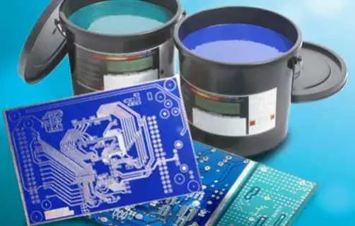
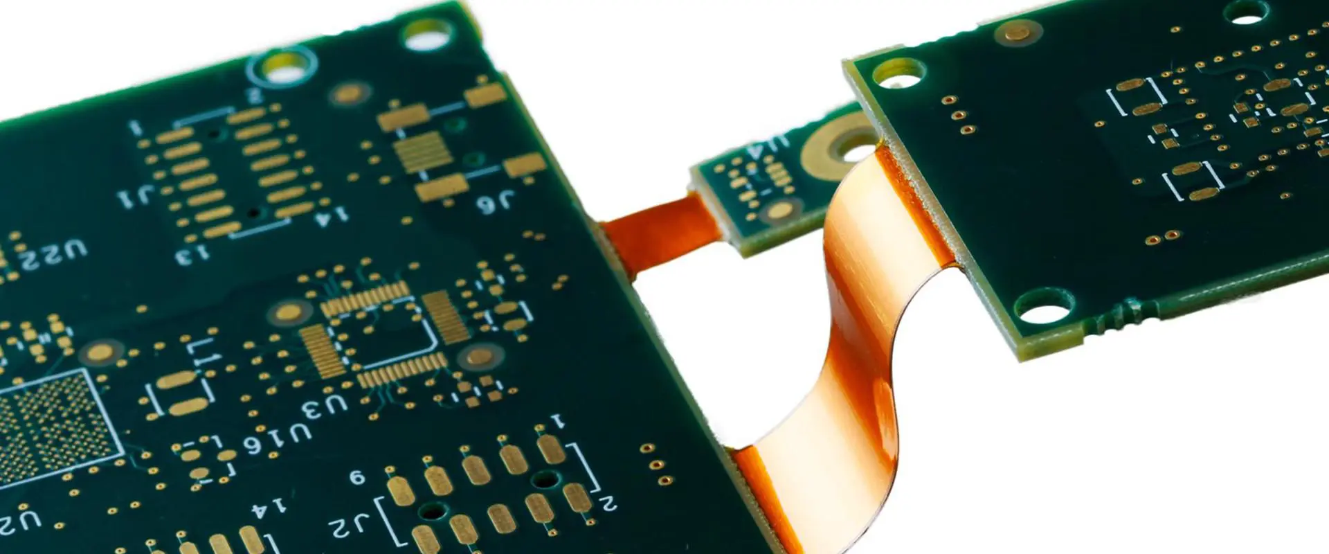
A PCB stencil is a thin sheet of material with precisely cut apertures that correspond to the areas on a PCB where solder paste or other materials need to be applied. When the stencil is placed over the PCB and solder paste is spread across it, the paste passes through the apertures and onto the designated areas of the board.

Importance of Stencils in PCB Manufacturing

Stencils play a critical role in the PCB assembly process for several reasons:

  1. Precision: They ensure accurate placement of solder paste on the PCB.
  2. Consistency: Stencils help maintain uniform solder paste volume across all components.
  3. Efficiency: They significantly speed up the paste application process compared to manual methods.
  4. Quality: Well-made stencils contribute to higher-quality solder joints and fewer defects.

Materials Used in PCB Stencil Making

smd stencil

The choice of material for a PCB stencil is crucial as it affects the stencil’s performance, durability, and suitability for different applications. The most common materials used are:

  1. Stainless Steel
  2. Nickel
  3. Polyimide (Kapton)
  4. Molybdenum

Let’s compare these materials in a table:

| Material | Advantages | Disadvantages | Best For | |———-|————|—————|———-| | Stainless Steel | Durable, cost-effective, suitable for fine-pitch applications | Can be heavy for large stencils | High-volume production, fine-pitch applications | | Nickel | Flexible, resistant to warping | More expensive than stainless steel | Stepped stencils, areas with high paste deposit requirements | | Polyimide | Very flexible, ideal for prototype runs | Limited lifespan, not suitable for high-volume production | Prototyping, low-volume production | | Molybdenum | Extremely durable, maintains shape well | Expensive, can be brittle | High-precision, high-volume production |

The Stencil Making Process

The process of making a PCB screen printing stencil involves several steps, each crucial to the final quality of the stencil. Let’s explore these steps in detail.

1. Design and Data Preparation

The first step in creating a PCB stencil is preparing the design data. This typically involves:

  • Extracting the solder paste layer from the PCB design file
  • Adjusting aperture sizes based on component requirements
  • Optimizing the design for the stencil cutting process

Design Considerations

When preparing the design, several factors need to be considered:

  • Aperture size and shape
  • Component pitch
  • Solder paste volume requirements
  • Board panelization

2. Material Selection

Based on the requirements of the PCB and the production run, an appropriate stencil material is selected. Factors influencing this choice include:

  • Production volume
  • Required stencil lifespan
  • Component density and pitch
  • Budget constraints

3. Cutting Method Selection

There are several methods for cutting PCB stencils, each with its own advantages and limitations:

Laser Cutting

Laser cutting is the most common method for creating PCB stencils. It offers high precision and is suitable for a wide range of materials.

Advantages of Laser Cutting:
  • High precision (typically ยฑ0.0005″)
  • Suitable for fine-pitch applications
  • Can cut complex shapes
  • No tool wear
Disadvantages of Laser Cutting:
  • Higher initial equipment cost
  • Potential for heat-affected zones in some materials

Chemical Etching

Chemical etching is an older method that is still used in some applications.

Advantages of Chemical Etching:
  • Can produce large stencils
  • No heat-affected zones
Disadvantages of Chemical Etching:
  • Less precise than laser cutting
  • Environmental concerns due to chemical use
  • Longer production time

Electroforming

Electroforming is used for creating high-precision stencils, particularly for ultra-fine pitch applications.

Advantages of Electroforming:
  • Extremely high precision
  • Smooth aperture walls
Disadvantages of Electroforming:
  • More expensive than other methods
  • Longer production time

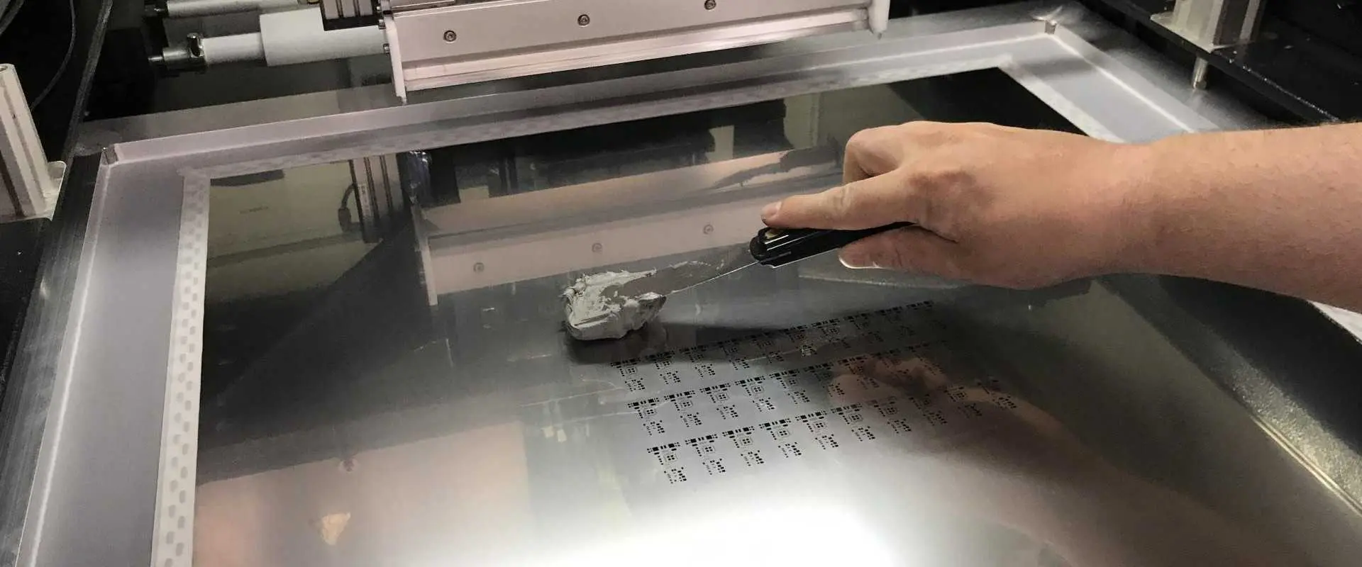
4. Stencil Cutting Process

Once the cutting method is selected, the actual stencil cutting process begins. For the most common method, laser cutting, the process typically involves:

  1. Loading the stencil material into the laser cutting machine
  2. Importing the prepared design data
  3. Setting up laser parameters (power, speed, focus)
  4. Executing the cutting process
  5. Inspecting the cut stencil for quality
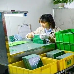
5. Post-Processing

After cutting, the stencil often undergoes additional processing steps:

Cleaning

The stencil is thoroughly cleaned to remove any debris from the cutting process. This may involve:

  • Ultrasonic cleaning
  • Chemical cleaning
  • Manual cleaning with specialized solvents

Surface Treatment

Some stencils undergo surface treatments to improve their performance:

  • Electropolishing: Smooths the aperture walls for better paste release
  • Nano-coating: Applies a non-stick coating to improve paste release and ease cleaning

Tensioning

For frame-mounted stencils, the cut foil is stretched and mounted onto a frame. This process, known as tensioning, ensures the stencil remains flat during use.
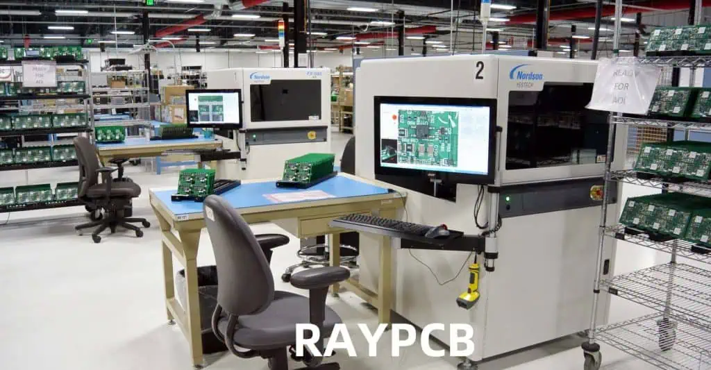
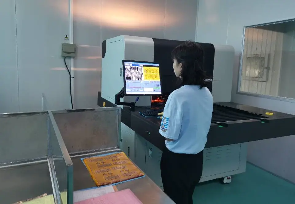
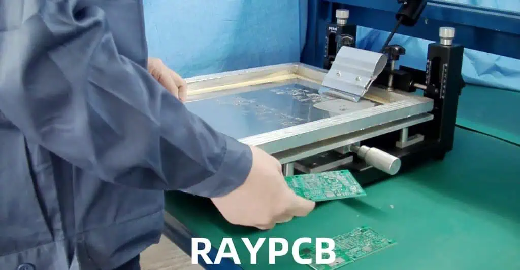
6. Quality Control

Quality control is a critical step in the stencil making process. It typically involves:

  • Visual inspection for defects
  • Dimensional verification using high-precision measurement tools
  • Aperture size and position verification
  • Test prints to ensure proper paste deposition

Stencil Design Considerations

Solder paste stencil frame

Creating an effective PCB stencil involves more than just cutting holes in a sheet of metal. Several design considerations can significantly impact the stencil’s performance:

Aperture Size and Shape

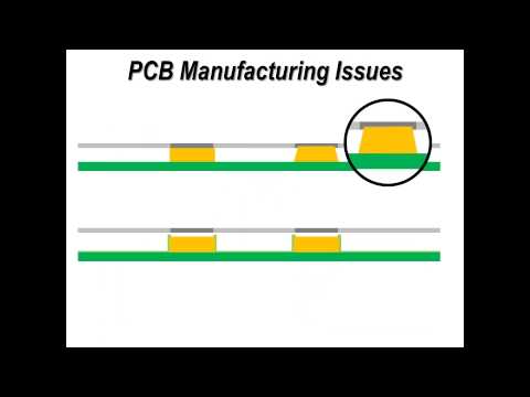
The size and shape of the stencil apertures are crucial for proper solder paste deposition. Some key points:

  • Aperture size is typically 10-20% smaller than the pad size
  • Shape can be square, rectangular, circular, or custom
  • Aspect ratio (thickness to width) should be considered for reliable paste release

Area Ratio

The area ratio is the ratio of the aperture area to its wall area. It’s a crucial factor in determining how well solder paste will release from the aperture.

| Area Ratio | Paste Release | |————|—————| | > 0.66 | Excellent | | 0.5 – 0.66 | Good | | < 0.5 | Poor |

Step Stencils

Step stencils have different thicknesses in different areas of the stencil. They’re used when components on the PCB require significantly different amounts of solder paste.

Home Plate Design

For components with large thermal pads, a “home plate” aperture design can help prevent solder balling and tombstoning.

Stencil Lifecycle and Maintenance

Proper care and maintenance can significantly extend the life of a PCB stencil:

Cleaning

Regular cleaning is crucial for maintaining stencil performance:

  • Clean after each use
  • Use appropriate cleaning solvents
  • Consider ultrasonic cleaning for thorough results

Storage

Proper storage helps prevent damage and contamination:

  • Store in a clean, dry environment
  • Use protective covers or cases
  • Avoid stacking heavy items on stencils

Inspection and Replacement

Regular inspection can catch issues before they affect production:

  • Check for wear, warping, or damage before each use
  • Replace stencils when signs of degradation appear
  • Keep backup stencils for critical production runs

Advanced Stencil Technologies

As PCB technology advances, so do stencil technologies. Some cutting-edge developments include:

Nano-Coated Stencils

Nano-coatings can significantly improve paste release and ease cleaning:

  • Hydrophobic coatings repel moisture
  • Oleophobic coatings repel oils
  • Can extend stencil life and improve print quality

3D Printed Stencils

While not yet widely used in production, 3D printed stencils show promise for rapid prototyping:

  • Quick turnaround for prototype runs
  • Potential for complex, custom designs
  • Currently limited by material properties and precision

Smart Stencils

Emerging “smart” stencil technologies incorporate sensors or markers:

  • Can detect misalignment or wear
  • May integrate with automated inspection systems
  • Potential for real-time process optimization

Conclusion

The PCB screen printing stencil making process is a critical aspect of PCB manufacturing that requires careful consideration of materials, design, and manufacturing techniques. A well-made stencil can significantly improve the quality and efficiency of PCB assembly, while a poor stencil can lead to defects and rework.

As PCB technology continues to advance, with components becoming smaller and boards more densely populated, the importance of high-quality, precision stencils will only increase. Staying informed about the latest stencil technologies and best practices is crucial for anyone involved in PCB manufacturing.

Frequently Asked Questions (FAQ)

1. How long does a typical PCB stencil last?

The lifespan of a PCB stencil can vary greatly depending on the material, usage, and maintenance. A well-maintained stainless steel stencil used in a high-volume production environment might last for 10,000 to 50,000 prints or more. However, factors like the complexity of the design, the abrasiveness of the solder paste, and the cleaning methods used can all affect the stencil’s lifespan.

2. Can I reuse a stencil for different PCB designs?

While it’s possible to reuse a stencil for different PCB designs in some cases, it’s generally not recommended. Each stencil is designed for a specific PCB layout, and using it for a different design could lead to misaligned solder paste deposits and potential defects. However, if the new design is a minor revision that doesn’t affect the areas where solder paste is applied, reuse might be possible.

3. What’s the difference between framed and frameless stencils?

Framed stencils are mounted on a rigid frame, usually made of aluminum. They maintain tension and flatness well, making them ideal for high-volume production. Frameless stencils, also known as foil stencils, are more flexible and can be easily stored, making them suitable for low-volume production or when storage space is limited. Frameless stencils typically require a separate tensioning system on the printer.

4. How do I choose between a laser-cut and a chemically etched stencil?

The choice between laser-cut and chemically etched stencils depends on several factors:

  • Precision: Laser-cut stencils generally offer higher precision, making them better for fine-pitch components.
  • Cost: Chemical etching can be more cost-effective for larger stencils or lower volumes.
  • Turnaround time: Laser cutting is typically faster, especially for small to medium-sized stencils.
  • Environmental concerns: Chemical etching involves hazardous chemicals, which may be a concern in some situations.

In most modern PCB manufacturing, laser-cut stencils are preferred due to their precision and versatility.

5. What’s the importance of the area ratio in stencil design?

The area ratio is crucial in stencil design as it directly affects how well the solder paste will release from the aperture. It’s calculated by dividing the area of the aperture by the area of its walls. A higher area ratio (generally above 0.66) ensures better paste release, resulting in more consistent solder paste deposits. For small components or fine-pitch applications where the area ratio might be low, special considerations in stencil design or manufacturing may be necessary to ensure proper paste release.

Manufacturing PCBs for Industrial Businesses: A Comprehensive Guide

Industrial IoT

Printed Circuit Boards (PCBs) serve as the backbone of modern industrial equipment, powering everything from factory automation systems to heavy machinery control units. For industrial businesses, understanding PCB manufacturing is crucial for developing reliable, cost-effective electronic solutions that can withstand harsh operating environments and meet stringent performance requirements.

Understanding Industrial PCB Requirements

Industrial PCBs differ significantly from consumer electronics boards in their design specifications and manufacturing requirements. These boards must operate reliably in extreme temperatures, resist chemical exposure, withstand mechanical vibrations, and maintain performance over extended periodsโ€”often decades. Industrial applications demand boards that can function in temperatures ranging from -40ยฐC to +125ยฐC, humidity levels up to 95%, and environments with significant electromagnetic interference.

The complexity of industrial PCBs varies considerably based on their application. Simple control boards might require only two layers, while sophisticated industrial computers or motor drives may need twelve or more layers to accommodate dense component placement and complex signal routing. High-power applications often require thick copper layers to handle substantial current loads, while precision measurement equipment demands exceptional signal integrity and minimal noise interference.

Key Manufacturing Considerations for Industrial PCBs

Material selection forms the foundation of successful industrial PCB manufacturing. FR-4 remains the most common substrate material due to its excellent balance of mechanical strength, electrical properties, and cost-effectiveness. However, specialized industrial applications may require alternative materials such as polyimide for flexible circuits, ceramic substrates for high-frequency applications, or metal-core boards for superior thermal management in power electronics.

Copper thickness represents another critical specification for industrial boards. Standard consumer boards typically use 1-ounce copper, but industrial applications often require 2-ounce or even 4-ounce copper to handle high current loads safely. Heavier copper weights improve current-carrying capacity and thermal dissipation but increase manufacturing complexity and cost.

Component placement and routing strategies must account for the harsh industrial environment. Critical components should be positioned away from high-heat areas, and sensitive analog circuits must be isolated from switching power supplies and digital circuits. Proper grounding techniques, including ground planes and strategic via placement, help minimize electromagnetic interference and improve overall system reliability.

The Industrial PCB Manufacturing Process

The manufacturing process for industrial PCBs follows similar steps to consumer boards but with enhanced quality control measures and specialized techniques. The process begins with design verification, where engineers review the board layout for manufacturability, ensuring trace widths can handle required currents, via sizes are appropriate for the layer count, and component footprints match actual parts.

Substrate preparation involves cutting the base material to size and drilling holes for component mounting and layer interconnection. Industrial boards often require precision drilling with tight tolerances to ensure proper component fit and reliable electrical connections. Advanced drilling techniques, such as laser drilling for microvias, may be necessary for high-density designs.

Layer stack-up and lamination require careful attention to impedance control and thermal management. Industrial boards frequently incorporate controlled impedance traces for high-speed signals, requiring precise control of trace geometry and dielectric properties. Multiple pressing cycles may be necessary for thick, multi-layer boards, with careful temperature and pressure control to prevent delamination or warpage.

Surface finishing plays a crucial role in industrial PCB reliability. While HASL (Hot Air Solder Leveling) remains common for cost-sensitive applications, many industrial boards benefit from more advanced finishes like ENIG (Electroless Nickel Immersion Gold) or OSP (Organic Solderability Preservative) for improved solderability and corrosion resistance.

Quality Control and Testing Standards

Industrial PCBs must meet rigorous quality standards that exceed typical consumer electronics requirements. IPC-A-600 provides the acceptability criteria for printed boards, while IPC-6012 establishes qualification and performance specifications. Many industrial applications also require compliance with specific industry standards such as IEC 61131 for programmable controllers or ISO 26262 for automotive safety systems.

Electrical testing encompasses continuity checks, insulation resistance measurements, and high-voltage testing to ensure the board can withstand operational stresses. Advanced testing may include impedance verification for high-speed signals, time-domain reflectometry for signal integrity analysis, and thermal cycling to validate solder joint reliability.

Visual inspection using automated optical inspection (AOI) systems helps identify manufacturing defects such as solder bridges, missing components, or improper component placement. X-ray inspection may be necessary for boards with ball grid array (BGA) components or other hidden solder joints that cannot be visually verified.

Cost Optimization Strategies

INDUSTRIAL Control Board

Managing costs while maintaining quality requires strategic planning and collaboration between design and manufacturing teams. Design for manufacturability (DFM) principles can significantly reduce production costs by minimizing layer count, using standard via sizes, and avoiding unnecessary tight tolerances.

Volume considerations play a major role in cost optimization. Industrial businesses should carefully forecast their requirements to take advantage of volume pricing breaks while avoiding excess inventory costs. Many manufacturers offer flexible scheduling options that allow customers to commit to annual volumes while releasing smaller quantities as needed.

Supplier selection involves balancing cost, quality, and service capabilities. While offshore manufacturing often provides the lowest unit costs, domestic suppliers may offer advantages in communication, shorter lead times, and better quality control for critical applications. Establishing relationships with multiple suppliers provides flexibility and reduces supply chain risks.

Supply Chain Management and Lead Times

Industrial PCB manufacturing requires careful supply chain management to ensure consistent availability of materials and components. Raw material shortages, particularly for specialized substrates or surface finishes, can significantly impact production schedules. Successful industrial businesses often maintain strategic inventory of critical materials or establish long-term supply agreements with key suppliers.

Lead times for industrial PCBs vary significantly based on complexity, quantity, and supplier capacity. Simple boards may be available in one to two weeks, while complex multi-layer boards with specialized materials might require four to eight weeks. Rush services are available but typically carry substantial cost premiums that may not be justified except for emergency situations.

Communication with manufacturing partners throughout the production process helps identify potential issues early and maintain schedule adherence. Regular design reviews, prototype validation, and production status updates ensure that both parties understand requirements and expectations.

Future Trends and Technologies

The industrial PCB manufacturing landscape continues to evolve with advancing technologies and changing market demands. Embedded components, where passive components are built directly into the PCB substrate, offer space savings and improved reliability for high-density applications. Advanced materials like low-loss dielectrics enable higher frequency operation for industrial IoT and wireless communication systems.

Additive manufacturing techniques, including 3D printing of conductive traces and embedded electronics, promise new possibilities for industrial PCB design and manufacturing. While still in early development stages, these technologies may eventually enable rapid prototyping and small-volume production of complex three-dimensional circuits.

Environmental considerations are driving development of lead-free processes, halogen-free materials, and recyclable substrates. Industrial businesses increasingly must consider the complete lifecycle environmental impact of their electronic products, from raw material extraction through end-of-life disposal.


Frequently Asked Questions

What makes industrial PCBs different from consumer electronics boards?

Industrial PCBs are designed to operate in much harsher environments with extreme temperatures, humidity, vibration, and chemical exposure. They typically require heavier copper layers, more robust materials, and enhanced quality control measures to ensure reliable operation over extended periods, often 10-20 years or more.

How do I determine the right copper weight for my industrial application?

Copper weight selection depends on the current requirements of your circuits. Use online current-carrying capacity calculators or consult IPC-2221 standards. Generally, 1-ounce copper handles up to 1-2 amps per trace, 2-ounce copper supports 2-4 amps, and 4-ounce copper can handle 4-8 amps, depending on trace width and temperature rise limits.

What are typical lead times for industrial PCB manufacturing?

Lead times vary from 1-2 weeks for simple, two-layer boards to 6-8 weeks for complex, multi-layer boards with specialized materials. Factors affecting lead time include layer count, board size, material availability, surface finish requirements, and manufacturer capacity. Always plan for potential delays and consider maintaining some safety stock for critical applications.

Should I choose domestic or offshore PCB manufacturing?

The choice depends on your priorities. Offshore manufacturing typically offers lower unit costs but may have longer lead times, communication challenges, and quality consistency issues. Domestic manufacturing provides better communication, shorter lead times, and often superior quality control, but at higher unit costs. Consider the total cost of ownership, including logistics, inventory, and potential quality issues.

What quality standards should industrial PCBs meet?

Most industrial PCBs should comply with IPC-A-600 for acceptability criteria and IPC-6012 for qualification requirements. Depending on your industry, additional standards may apply, such as IEC 61131 for industrial automation, ISO 26262 for automotive applications, or DO-254 for aerospace systems. Discuss specific requirements with your manufacturer to ensure compliance.

How can I reduce PCB manufacturing costs without compromising quality?

Focus on design for manufacturability by using standard materials, minimizing layer count, avoiding tight tolerances unless necessary, and designing for volume production. Consider panelization to improve manufacturing efficiency, standardize board sizes across products, and establish long-term supplier relationships for better pricing. Regular design reviews with your manufacturer can identify cost-saving opportunities.

What surface finish is best for industrial applications?

ENIG (Electroless Nickel Immersion Gold) is often preferred for industrial applications due to its excellent corrosion resistance, flat surface for fine-pitch components, and long shelf life. OSP is cost-effective for simple applications, while HASL remains common for through-hole components. The choice depends on your specific requirements for component types, environmental exposure, and shelf life needs.

Manufacturing PCBs for the Telecommunication Industry

The telecommunications industry represents one of the most demanding sectors for printed circuit board (PCB) manufacturing, requiring exceptional precision, reliability, and performance standards. As the backbone of modern communication infrastructure, telecommunication PCBs must operate flawlessly in diverse environments while handling complex signal processing, high-frequency transmissions, and stringent regulatory requirements. This comprehensive overview explores the specialized manufacturing processes, materials, and considerations essential for producing PCBs that meet the exacting demands of telecommunication applications.

Unique Requirements and Challenges

Telecommunication PCBs face distinctive challenges that set them apart from consumer electronics or standard industrial applications. These boards must maintain signal integrity across a wide frequency spectrum, often ranging from low-frequency control signals to high-frequency radio transmissions exceeding several gigahertz. The industry demands exceptional reliability, as network downtime can result in significant economic losses and service disruptions affecting millions of users.

Environmental resilience stands as another critical requirement. Telecommunication equipment operates in cellular towers exposed to extreme weather conditions, underground installations with high humidity, and data centers with varying temperature conditions. PCBs must withstand temperature fluctuations from -40ยฐC to +85ยฐC while maintaining consistent electrical performance. Additionally, these boards often require extended operational lifespans, sometimes exceeding 20 years, demanding superior material selection and manufacturing processes.

Signal integrity becomes particularly crucial in high-speed digital communications and RF applications. Telecommunication PCBs must minimize electromagnetic interference (EMI), crosstalk, and signal distortion while maximizing transmission efficiency. This requires precise impedance control, careful layer stack-up design, and specialized manufacturing techniques to achieve the necessary electrical characteristics.

Specialized Materials and Substrates

The selection of appropriate materials forms the foundation of successful telecommunication PCB manufacturing. Traditional FR-4 materials, while suitable for many applications, often prove inadequate for high-frequency telecommunication circuits. Instead, manufacturers typically employ advanced dielectric materials with lower dielectric constants and dissipation factors to minimize signal loss and maintain performance at high frequencies.

Rogers materials, including RO4000 and RO3000 series, have become industry standards for high-frequency applications. These materials offer excellent electrical properties, including stable dielectric constants across frequency ranges and low loss tangents that preserve signal integrity. For extremely demanding applications, manufacturers may utilize PTFE-based materials or specialized ceramic-filled composites that provide superior performance but require modified processing techniques.

Metal core PCBs find applications in power amplifier circuits and base station equipment where thermal management is critical. These boards utilize aluminum or copper cores to efficiently dissipate heat generated by high-power components, ensuring reliable operation and extended component lifecycles. The thermal interface materials and manufacturing processes for metal core boards require specialized expertise and equipment.

Flexible and rigid-flexible PCBs address space constraints and mechanical requirements in modern telecommunication equipment. These boards enable compact designs while accommodating movement and vibration in mobile applications. The manufacturing of flexible circuits requires specialized polyimide substrates and modified processing techniques to maintain flexibility while ensuring reliable electrical connections.

Manufacturing Process Considerations

Telecommunication PCB manufacturing demands enhanced process control and precision compared to standard PCB production. Layer stack-up design requires careful consideration of signal layers, power planes, and ground planes to achieve optimal electrical performance. Manufacturers must precisely control dielectric thickness to maintain impedance requirements, often requiring specialized prepreg materials and controlled pressing cycles.

Via technology plays a crucial role in high-frequency designs. Blind and buried vias minimize signal path lengths and reduce parasitic effects, while microvias enable high-density interconnections. The drilling and plating processes for these features require advanced equipment and tight process control to ensure consistent results. Manufacturers often employ laser drilling for microvias and mechanical drilling for larger features, each requiring specific parameter optimization.

Plating processes for telecommunication PCBs often involve specialized finishes to enhance performance and reliability. While traditional HASL (Hot Air Solder Leveling) may suffice for some applications, high-frequency circuits often require more sophisticated finishes such as ENIG (Electroless Nickel Immersion Gold) or OSP (Organic Solderability Preservative) to minimize signal loss and ensure consistent electrical properties.

Surface mount technology (SMT) considerations become critical when manufacturing PCBs for telecommunication applications. Fine-pitch components, ball grid arrays (BGAs), and high-power devices require precise pad geometries and solder mask design. The manufacturing process must accommodate these requirements while maintaining electrical performance and thermal management capabilities.

Quality Control and Testing

Quality control in telecommunication PCB manufacturing extends far beyond standard electrical testing. High-frequency performance verification requires specialized test equipment capable of measuring parameters such as insertion loss, return loss, and crosstalk across the operational frequency range. Time-domain reflectometry (TDR) testing helps identify impedance discontinuities that could degrade signal quality.

Environmental testing becomes particularly important for telecommunication applications. Thermal cycling tests verify board reliability across temperature extremes, while humidity testing ensures performance in challenging environmental conditions. Vibration and shock testing confirm mechanical integrity for mobile and outdoor applications.

Automated optical inspection (AOI) and automated X-ray inspection (AXI) systems help identify manufacturing defects that could compromise performance or reliability. These systems must be programmed with appropriate algorithms and acceptance criteria specific to telecommunication applications, considering the critical nature of these circuits.

Statistical process control (SPC) implementation helps manufacturers maintain consistent quality while identifying trends that could indicate process drift. Regular capability studies and process validation ensure that manufacturing processes remain within specification limits and continue to meet customer requirements.

Regulatory Compliance and Standards

Telecommunication PCBs must comply with numerous industry standards and regulatory requirements. IPC standards, including IPC-2221 for generic PCB design and IPC-6012 for qualification and performance specifications, provide fundamental guidelines for manufacturing quality. However, telecommunication applications often require compliance with additional standards specific to the industry.

EMC (Electromagnetic Compatibility) requirements demand careful attention to PCB design and manufacturing processes. Proper grounding techniques, shielding considerations, and layout optimization help ensure compliance with regulatory limits for electromagnetic emissions and susceptibility. Manufacturing processes must maintain these design intentions while avoiding practices that could compromise EMC performance.

Safety standards, including UL recognition and international safety certifications, may apply depending on the specific application and market requirements. These standards often dictate material selection, construction methods, and testing requirements that influence manufacturing processes.

RoHS compliance and other environmental regulations restrict the use of certain materials and processes in PCB manufacturing. Telecommunication equipment manufacturers increasingly demand lead-free processes and environmentally friendly materials, requiring manufacturers to adapt their processes accordingly.

Future Trends and Innovations

The telecommunication industry continues to evolve rapidly, driving new requirements for PCB manufacturing. The rollout of 5G networks demands PCBs capable of operating at millimeter-wave frequencies with minimal loss and exceptional thermal performance. This requires continued advancement in materials science and manufacturing techniques.

Embedded component technology, where passive components are integrated directly into the PCB substrate, offers opportunities for miniaturization and improved electrical performance. However, these technologies require specialized manufacturing processes and equipment that many manufacturers are still developing.

Advanced packaging technologies, including system-in-package (SiP) and 3D integration, present new challenges and opportunities for telecommunication PCB manufacturers. These approaches require close collaboration between PCB manufacturers, component suppliers, and equipment manufacturers to develop integrated solutions.

The increasing emphasis on sustainability and environmental responsibility drives innovation in materials and processes. Biodegradable substrates, recycling programs, and energy-efficient manufacturing processes represent areas of active development that will influence future telecommunication PCB manufacturing.

Conclusion

Manufacturing PCBs for the telecommunication industry requires specialized expertise, advanced materials, and precise process control to meet the demanding requirements of modern communication systems. Success in this market depends on understanding the unique challenges of high-frequency design, environmental resilience, and long-term reliability while maintaining compliance with industry standards and regulatory requirements. As the telecommunication industry continues to evolve with 5G deployment and future technologies, PCB manufacturers must continue to innovate and adapt their processes to meet these emerging challenges while maintaining the highest standards of quality and performance.

Selecting the Most Suitable PCB Contract Manufacturer

Choosing the right printed circuit board (PCB) contract manufacturer is one of the most critical decisions in bringing an electronic product to market. The quality, reliability, and cost-effectiveness of your final product largely depend on this partnership. With the global PCB manufacturing market valued at over $70 billion and continuing to grow, the number of available manufacturers can be overwhelming. Making an informed decision requires careful evaluation of multiple factors that align with your specific project requirements and business objectives.

Understanding Your PCB Requirements

Before evaluating potential manufacturers, you must clearly define your project specifications. PCB complexity varies dramatically, from simple single-layer boards used in basic electronics to complex multi-layer boards with high-density interconnects required for advanced computing applications. Consider the number of layers needed, trace width and spacing requirements, via sizes, surface finishes, and any special materials like high-frequency substrates or flexible circuits.

Volume requirements significantly impact manufacturer selection. Low-volume prototyping demands different capabilities than high-volume production runs. Some manufacturers excel at quick-turn prototypes with minimal setup costs, while others are optimized for large-scale production with economies of scale. Your projected volumes over the product lifecycle should guide this evaluation.

Quality standards represent another crucial consideration. Industries like aerospace, medical devices, and automotive have stringent requirements that mandate specific certifications and quality management systems. Understanding which standards apply to your application ensures you select a manufacturer capable of meeting these requirements consistently.

Evaluating Manufacturing Capabilities

Technical capabilities form the foundation of manufacturer evaluation. Assess whether potential partners can handle your specific PCB requirements, including minimum trace widths, via sizes, layer counts, and board thicknesses. Advanced applications may require capabilities like blind and buried vias, controlled impedance, or specialized surface finishes like ENIG or OSP.

Manufacturing capacity and scalability are equally important. A manufacturer might handle your initial volumes effectively but struggle to scale up for mass production. Evaluate their production capacity, equipment availability, and ability to accommodate growth in your orders. Consider their backup plans for equipment failures and their ability to maintain consistent delivery schedules during peak demand periods.

Geographic location affects logistics, communication, and supply chain resilience. Domestic manufacturers often provide better communication, shorter lead times, and reduced shipping costs, but may have higher labor costs. Overseas manufacturers, particularly in Asia, frequently offer competitive pricing but may present challenges in communication, quality control, and intellectual property protection.

Quality Assurance and Certifications

Quality management systems provide insight into a manufacturer’s commitment to consistent production standards. Look for certifications like ISO 9001 for general quality management, AS9100 for aerospace applications, ISO 13485 for medical devices, or TS 16949 for automotive applications. These certifications indicate established processes for quality control, continuous improvement, and risk management.

Testing capabilities are crucial for ensuring PCB reliability. Evaluate the manufacturer’s testing equipment and procedures, including automated optical inspection (AOI), in-circuit testing (ICT), functional testing, and environmental stress testing. Advanced manufacturers offer comprehensive test reports and statistical process control data to demonstrate quality consistency.

Traceability systems become critical for regulated industries and complex supply chains. Manufacturers should maintain detailed records of materials, processes, and test results for each batch or individual board. This capability proves essential for quality investigations, recalls, or regulatory audits.

Supply Chain and Materials Management

Material sourcing capabilities directly impact cost, quality, and delivery reliability. Manufacturers with strong supplier relationships can often secure better pricing on raw materials and components while maintaining consistent quality. Evaluate their approved vendor lists, material qualification processes, and inventory management systems.

Supply chain resilience has become increasingly important following recent global disruptions. Assess the manufacturer’s risk management strategies, including multiple supplier relationships, inventory buffers, and contingency planning. Manufacturers with diversified supply chains are better positioned to maintain production during supply disruptions.

Obsolescence management represents a long-term consideration for products with extended lifecycles. Understanding how manufacturers handle component obsolescence, alternative sourcing, and design modifications ensures continued production availability throughout your product’s market life.

Cost Considerations and Pricing Models

Understanding pricing structures helps make informed cost comparisons. Some manufacturers use tooling charges, setup fees, and minimum order quantities that significantly impact total costs, especially for low-volume orders. Others operate with all-inclusive pricing that simplifies cost calculations but may be less competitive for large volumes.

Hidden costs can substantially impact total project expenses. Consider expenses beyond the basic manufacturing cost, including tooling, setup charges, testing fees, shipping costs, and potential expedite charges. International manufacturers may present additional costs like customs duties, currency fluctuations, and extended logistics expenses.

Value engineering services from experienced manufacturers can reduce overall costs through design optimization recommendations. Manufacturers familiar with cost-effective design practices can suggest modifications that maintain functionality while reducing manufacturing complexity and costs.

Communication and Project Management

Communication effectiveness directly impacts project success, particularly for complex designs or tight schedules. Evaluate the manufacturer’s communication channels, response times, and technical support capabilities. Language barriers, time zone differences, and cultural factors can complicate international partnerships.

Project management capabilities become crucial for complex projects with multiple stakeholders and tight deadlines. Look for manufacturers with dedicated project managers, established milestone tracking systems, and proactive communication regarding potential issues or delays.

Documentation standards affect both initial development and ongoing production support. Manufacturers should provide comprehensive fabrication drawings, assembly instructions, test procedures, and quality reports. Clear documentation reduces misunderstandings and supports consistent production quality.

Building Long-term Partnerships

Successful PCB manufacturing relationships extend beyond individual projects to long-term strategic partnerships. Evaluate potential manufacturers as partners who will support your business growth, provide technical expertise, and contribute to product development success.

Flexibility and responsiveness become important as market conditions change and new opportunities arise. Manufacturers who can accommodate design changes, adjust production schedules, and support new product introductions provide valuable competitive advantages.

Technology roadmaps and investment in advanced capabilities indicate a manufacturer’s commitment to staying current with industry developments. Partners who invest in new equipment, processes, and certifications can support your products as technology requirements evolve.

Frequently Asked Questions

Q: How do I determine if a PCB manufacturer can handle my specific requirements? A: Request detailed capability sheets showing their technical specifications, including minimum trace widths, via sizes, layer counts, and material options. Ask for samples of similar complexity boards they’ve produced and discuss any unique requirements during initial consultations.

Q: What’s the difference between choosing a domestic versus overseas PCB manufacturer? A: Domestic manufacturers typically offer better communication, shorter lead times, easier quality control, and stronger IP protection, but usually at higher costs. Overseas manufacturers often provide competitive pricing but may present challenges in communication, quality oversight, and logistics.

Q: How important are industry certifications when selecting a PCB manufacturer? A: Industry certifications are crucial, especially for regulated industries. ISO 9001 demonstrates basic quality management, while specialized certifications like AS9100 (aerospace), ISO 13485 (medical), or TS 16949 (automotive) are often mandatory for those applications.

Q: Should I choose a manufacturer based primarily on price? A: Price is important but shouldn’t be the sole deciding factor. Consider total cost of ownership, including quality, reliability, delivery performance, and potential rework costs. A slightly higher-priced manufacturer with better quality and service often provides better overall value.

Q: How can I protect my intellectual property when working with PCB manufacturers? A: Use comprehensive non-disclosure agreements, work with manufacturers in countries with strong IP protection laws, limit design information sharing to essential details, and consider using trusted domestic manufacturers for sensitive designs.

Q: What should I expect in terms of lead times for PCB manufacturing? A: Lead times vary significantly based on complexity, volume, and manufacturer capacity. Simple prototypes might be completed in 3-5 days, while complex multi-layer boards could require 2-3 weeks. Production volumes typically require longer lead times for setup and manufacturing.

Q: How do I evaluate a manufacturer’s quality before placing orders? A: Review their certifications, request customer references, ask for sample boards of similar complexity, visit their facilities if possible, and start with small prototype orders to evaluate their quality and service before committing to larger volumes.

Selecting the right PCB contract manufacturer requires balancing multiple factors including technical capabilities, quality systems, cost considerations, and long-term partnership potential. Taking time to thoroughly evaluate these factors upfront pays dividends in product quality, cost-effectiveness, and successful market introduction.

Best Practices for Solder Resist on PCBs

Solder resist, also known as solder mask, is one of the most critical protective layers in printed circuit board (PCB) manufacturing. This thin polymer coating serves as a barrier between the copper traces and the external environment while providing precise openings for component soldering. Understanding and implementing best practices for solder resist application can significantly impact the reliability, manufacturability, and longevity of electronic assemblies.

YouTube video

Understanding Solder Resist Fundamentals

Solder resist primarily functions as an insulating layer that prevents solder bridges between adjacent copper features during the assembly process. Beyond its protective role, it also shields copper traces from oxidation, contamination, and physical damage. The material typically consists of epoxy-based polymers with photoinitiators that allow for precise patterning through photolithographic processes.

The most common solder resist colors include green, blue, red, black, white, and yellow, with green being the industry standard due to its excellent contrast for inspection and testing. The choice of color can affect both manufacturing processes and end-use applications, with darker colors potentially causing thermal management challenges and lighter colors offering better optical inspection capabilities.

Design Considerations for Optimal Performance

Proper solder resist design begins with understanding minimum feature sizes and clearances. Most PCB manufacturers specify minimum solder resist opening sizes, typically ranging from 0.10mm to 0.15mm depending on the fabrication process. Designing openings smaller than these specifications can result in incomplete resist removal, leading to soldering difficulties and potential assembly failures.

Solder resist expansion and contraction relative to copper pads requires careful consideration. The resist opening should be larger than the underlying copper pad to ensure complete exposure and account for registration tolerances during manufacturing. A typical expansion of 0.05mm to 0.10mm beyond the copper pad perimeter provides adequate margin for most applications.

Web width between adjacent solder resist openings represents another critical design parameter. Insufficient web width can cause resist to tear or lift during thermal cycling, compromising protection. Industry standards typically recommend minimum web widths of 0.10mm to 0.15mm, though this varies based on resist thickness and substrate material.

Application Methods and Process Control

Screen printing remains the most widely used method for solder resist application, offering excellent control over thickness and coverage. The process involves forcing resist material through a mesh screen onto the PCB surface, followed by tacking and developing stages. Proper screen selection, squeegee pressure, and printing speed directly influence the final resist quality.

Curtain coating provides an alternative application method suitable for high-volume production. This technique involves passing PCBs through a curtain of liquid resist, resulting in highly uniform thickness distribution. While offering excellent repeatability, curtain coating requires precise process control and may not be suitable for all board geometries.

Spray coating applications offer advantages for prototyping and low-volume production, providing good coverage of complex three-dimensional features. However, achieving consistent thickness and avoiding overspray requires careful equipment setup and environmental control.

Thickness Optimization and Uniformity

Solder resist thickness significantly impacts both protection and soldering performance. Typical thickness ranges from 20 to 40 micrometers, with thicker applications providing better protection but potentially causing soldering difficulties due to reduced heat transfer to component pads.

Achieving uniform thickness across the entire PCB surface requires attention to several factors. Board warpage can cause thickness variations during application, necessitating proper substrate handling and support. Edge effects often result in thicker resist buildup at board perimeters, which may require process adjustments or design modifications.

Non-uniform thickness can also result from inadequate surface preparation. Copper surface roughness, contamination, or oxide layers can interfere with resist adhesion and leveling. Proper cleaning and surface treatment protocols ensure optimal resist performance and uniformity.

Adhesion and Surface Preparation

Excellent adhesion between solder resist and the underlying substrate is essential for long-term reliability. Surface preparation plays a crucial role in achieving optimal adhesion, beginning with thorough cleaning to remove oils, fingerprints, and other contaminants that could interfere with bonding.

Mechanical surface treatment through micro-etching or abrasive cleaning creates microscopic texture that enhances mechanical bonding. However, excessive surface roughening can trap air bubbles and create uneven resist surfaces, requiring careful process optimization.

Chemical surface treatments, including coupling agents and adhesion promoters, can significantly improve bonding between organic resist materials and inorganic substrates. These treatments modify surface chemistry to create stronger chemical bonds while maintaining compatibility with subsequent processing steps.

Curing Process Optimization

PCB solder mask expose machine

Proper curing transforms liquid resist into a cross-linked polymer network with optimal mechanical and electrical properties. UV curing systems must provide adequate energy density across the entire spectrum required for complete photoinitiator activation. LED-based curing systems offer advantages in energy efficiency and spectral control compared to traditional mercury vapor lamps.

Thermal post-curing following UV exposure ensures complete cross-linking and removes residual solvents that could affect long-term performance. Temperature profiles must be carefully controlled to avoid thermal shock while achieving complete cure. Typical post-cure temperatures range from 140ยฐC to 160ยฐC for durations of 30 to 60 minutes.

Oxygen inhibition during UV curing can prevent complete surface cure, resulting in tacky or incompletely cross-linked surfaces. Nitrogen blanketing or other inert atmosphere techniques eliminate oxygen interference and ensure consistent cure quality.

Development and Imaging Precision

Accurate pattern development requires precise control of developer concentration, temperature, and contact time. Over-development can cause undercutting and loss of fine features, while under-development leaves resist residues that interfere with soldering and component placement.

Developer solution maintenance involves monitoring concentration through titration or conductivity measurements. Spent developer solutions lose effectiveness and can deposit contaminants on PCB surfaces, necessitating regular replacement or reconstitution.

Imaging precision depends on proper mask-to-substrate contact and adequate UV exposure. Contact printing requires uniform pressure distribution to ensure sharp edge definition, while projection imaging systems offer advantages for high-resolution features but require careful optical alignment.

Quality Control and Inspection Methods

Visual inspection remains the primary quality control method for solder resist, examining coverage completeness, color uniformity, and defect presence. Automated optical inspection (AOI) systems provide consistent, high-speed evaluation of resist quality while documenting results for process control.

Dimensional measurements verify that resist openings meet design specifications and manufacturing tolerances. Coordinate measuring machines or optical measurement systems provide accurate dimensional data for statistical process control.

Adhesion testing through tape pull or cross-hatch methods evaluates bonding quality between resist and substrate. These destructive tests provide quantitative data on adhesion strength but require sampling plans that balance quality assurance with production efficiency.

Common Defects and Prevention Strategies

Resist lifting or delamination typically results from poor surface preparation, contamination, or thermal stress during processing. Prevention strategies include improved cleaning protocols, surface treatment optimization, and thermal profile adjustments to minimize stress.

Pinholes and voids in resist coverage can expose copper traces to environmental attack and create potential reliability issues. These defects often originate from trapped air bubbles during application or inadequate surface wetting. Vacuum deaeration and proper rheological properties help eliminate bubble formation.

Color variations and mottling can result from incomplete mixing, contamination, or uneven curing. Maintaining consistent material properties through proper storage and handling prevents most color-related defects.

Environmental and Reliability Considerations

Long-term exposure to temperature cycling, humidity, and UV radiation can degrade solder resist properties over time. Material selection should consider the intended operating environment and expected service life. High-temperature applications may require specialized resist formulations with enhanced thermal stability.

Chemical resistance becomes important in harsh environments where PCBs may encounter solvents, acids, or other aggressive chemicals. Testing protocols should evaluate resist performance under expected exposure conditions to ensure adequate protection throughout the product lifecycle.

Thermal cycling reliability depends on the coefficient of thermal expansion matching between resist and substrate materials. Mismatched expansion rates can create stress concentrations that lead to cracking or delamination during temperature excursions.

Future Trends and Advanced Technologies

Emerging solder resist technologies focus on improved performance characteristics and environmental compatibility. Halogen-free formulations address environmental concerns while maintaining electrical and mechanical properties. Low-temperature cure systems reduce processing energy requirements and enable temperature-sensitive substrate compatibility.

Advanced application techniques, including inkjet printing and selective coating methods, offer potential advantages in precision and material efficiency. These technologies may enable new design possibilities while reducing waste and processing costs.

Integration with additive manufacturing processes represents an emerging application area where solder resist properties must be optimized for three-dimensional circuit structures and novel substrate materials.

Implementing these best practices for solder resist application ensures optimal PCB performance, reliability, and manufacturability while supporting the demanding requirements of modern electronic systems.

How to Make PCBs More Reliable

rigid flex PCB

Printed Circuit Board (PCB) reliability is fundamental to the success of any electronic product. Whether designing consumer electronics, automotive systems, or critical infrastructure equipment, engineers must prioritize reliability from the earliest design phases through manufacturing and deployment. A reliable PCB ensures consistent performance, reduces warranty costs, and maintains customer trust while minimizing field failures that can be costly and dangerous.

Understanding PCB Reliability Fundamentals

PCB reliability encompasses the board’s ability to perform its intended function without failure over its expected operational lifetime under specified environmental conditions. Reliability failures can manifest as intermittent connections, complete circuit failure, component degradation, or physical board damage. These failures often result from thermal stress, moisture ingress, mechanical fatigue, electrical overstress, or manufacturing defects that compound over time.

The key to reliable PCB design lies in understanding failure mechanisms and implementing preventive measures during design, material selection, manufacturing, and testing phases. Reliability engineering requires a systematic approach that considers the entire product lifecycle, from initial specifications through end-of-life disposal.

Design Considerations for Enhanced Reliability

Proper design forms the foundation of PCB reliability. Circuit layout decisions significantly impact long-term performance, making careful consideration of trace routing, component placement, and thermal management essential from the project’s inception.

Trace design plays a crucial role in reliability. Wide traces reduce resistance and heat generation, while maintaining appropriate spacing prevents crosstalk and reduces the likelihood of electrical shorts. Designers should avoid sharp angles in trace routing, instead using curved or 45-degree angles to minimize stress concentrations that can lead to copper cracking. Via placement requires careful attention, as excessive via density can weaken the board mechanically, while inadequate via coverage can create thermal bottlenecks.

Component placement strategy directly affects reliability outcomes. Heat-generating components should be distributed evenly across the board to prevent thermal hotspots, with adequate spacing for heat dissipation. Critical components require protection from mechanical stress points, while sensitive analog circuits need isolation from digital switching noise sources. Power distribution networks must be designed with sufficient copper area and multiple paths to ensure stable voltage delivery under varying load conditions.

Thermal management represents one of the most critical aspects of reliable PCB design. Elevated temperatures accelerate most failure mechanisms, making effective heat dissipation paramount. Thermal vias help conduct heat away from components to ground planes or heat sinks, while copper pours provide additional thermal mass. Strategic component placement keeps temperature-sensitive devices away from heat sources, and thermal simulation during design validation helps identify potential problem areas before manufacturing.

Material Selection and Quality

The choice of PCB materials significantly influences reliability outcomes. Standard FR-4 materials work well for many applications, but high-reliability designs may require specialized materials with enhanced thermal, mechanical, or electrical properties.

Substrate materials must match the application’s thermal expansion requirements. Coefficient of thermal expansion (CTE) mismatches between the PCB and mounted components create mechanical stress during temperature cycling, potentially leading to solder joint failures or component cracking. High-temperature applications may require polyimide or ceramic substrates that maintain dimensional stability across wider temperature ranges.

Copper quality and thickness affect both electrical performance and mechanical reliability. Higher copper weights provide better current-carrying capacity and thermal conductivity but increase manufacturing costs and board thickness. The copper foil type and surface roughness influence adhesion to the substrate material, with smoother surfaces generally providing better high-frequency performance but potentially reduced mechanical bonding.

Solder mask and surface finish selections impact long-term reliability. Quality solder masks protect copper traces from oxidation and provide insulation between conductors, while appropriate surface finishes ensure reliable solderability over extended storage periods. HASL (Hot Air Solder Leveling), ENIG (Electroless Nickel Immersion Gold), and OSP (Organic Solderability Preservative) each offer different advantages depending on the application requirements and assembly processes.

Manufacturing Process Controls

FQC inspection

Consistent manufacturing processes are essential for reliable PCB production. Process variations can introduce defects that may not manifest as immediate failures but can reduce long-term reliability through accelerated aging mechanisms.

Drilling operations require precise control to maintain hole quality and dimensional accuracy. Dull drill bits can cause rough hole walls or delamination around via sites, creating potential failure points. Proper drill bit selection, feed rates, and spindle speeds help maintain hole quality throughout production runs. Debris removal and desmearing processes ensure clean hole walls for reliable plating adhesion.

Plating processes must be carefully controlled to achieve uniform copper thickness and adhesion. Bath chemistry, temperature, and current density all affect plating quality. Non-uniform plating can create weak points in conductors, while poor adhesion between plating layers can lead to delamination failures. Regular bath analysis and test coupon evaluation help maintain consistent plating quality.

Etching processes require precise timing and chemistry control to achieve accurate trace dimensions without undercutting or rough edges. Over-etching can narrow traces below design specifications, increasing resistance and reducing current-carrying capacity. Under-etching may leave copper residues that can cause shorts between adjacent conductors.

Lamination processes must achieve proper bonding between layers while maintaining dimensional stability. Incorrect temperature, pressure, or timing can result in delamination, void formation, or warpage that affects component mounting and long-term reliability. Prepreg selection and handling procedures significantly influence lamination quality.

Environmental Stress Testing

Comprehensive testing validates PCB reliability under expected operating conditions and helps identify potential failure modes before product deployment. Environmental stress testing should simulate the actual operating environment as closely as possible while accelerating aging mechanisms to predict long-term performance.

Thermal cycling tests subject PCBs to repeated temperature excursions that simulate power cycling or environmental temperature variations. These tests reveal solder joint fatigue, component lead fatigue, and thermal expansion-related failures. Test parameters should reflect actual operating conditions, including temperature ranges, ramp rates, and dwell times.

Humidity testing evaluates moisture resistance and helps identify potential corrosion or electrical leakage issues. High humidity environments can cause conductor corrosion, insulation resistance degradation, and electrochemical migration between conductors. Combined temperature and humidity testing provides more realistic stress conditions than either test alone.

Vibration and shock testing assess mechanical robustness under transportation and operational stresses. These tests can reveal weak solder joints, component mounting issues, or board flexure problems that might not appear under static conditions. Test frequencies and amplitudes should represent actual mechanical environments the product will encounter.

Quality Control and Inspection

An electronic technician working on computer motherboard, inspection electronic connections and electronic parts with a microscope

Rigorous quality control throughout the manufacturing process helps identify and eliminate defects before they reach customers. Multiple inspection points allow for early defect detection and process correction.

Automated optical inspection (AOI) systems can detect many surface defects including missing components, incorrect component placement, solder bridging, and insufficient solder joints. These systems provide consistent inspection capability and can identify defects that might be missed during manual inspection. However, AOI systems require proper programming and maintenance to remain effective.

In-circuit testing (ICT) verifies electrical connectivity and component values but may not detect all reliability-related issues. Flying probe testing offers flexibility for prototype and low-volume production but may not achieve the throughput required for high-volume manufacturing. Functional testing provides the most comprehensive verification but requires custom test fixtures and procedures.

X-ray inspection reveals hidden defects in ball grid array (BGA) components, through-hole solder joints, and internal via connections. This non-destructive testing method can identify voids, insufficient solder, and other defects that affect long-term reliability but may not cause immediate functional failures.

Design for Manufacturability and Reliability

Integrating manufacturability considerations into the design process improves both production yields and long-term reliability. Design rules that facilitate consistent manufacturing typically also enhance reliability by reducing process-induced stress and defects.

Component selection should consider not only electrical performance but also package reliability and supply chain stability. Packages with proven reliability records and established manufacturing processes typically exhibit fewer field failures than newer, less mature technologies. Standard component footprints and orientations simplify assembly processes and reduce the likelihood of placement errors.

Design rule compliance ensures compatibility with manufacturing capabilities while minimizing process-induced defects. Minimum trace widths, via sizes, and spacing requirements should align with manufacturing capabilities while providing adequate margins for process variations. Consistent design practices across multiple projects facilitate manufacturing learning and process optimization.

Documentation quality directly impacts manufacturing consistency and reliability outcomes. Clear assembly drawings, comprehensive bill of materials, and detailed fabrication specifications help ensure that manufacturing processes align with design intent. Regular communication between design and manufacturing teams helps identify potential issues early in the development process.

The pursuit of PCB reliability requires a comprehensive approach that encompasses design methodology, material selection, manufacturing process control, and validation testing. Success depends on understanding failure mechanisms, implementing appropriate preventive measures, and maintaining rigorous quality standards throughout the entire product development and manufacturing lifecycle. By following these principles and continuously improving processes based on field experience and advancing technology, engineers can achieve the high reliability levels demanded by today’s sophisticated electronic systems.

Factors Affecting Print Quality of SMT Solder Paste

Solder paste stencil frame

Surface Mount Technology (SMT) has revolutionized electronic manufacturing by enabling the production of smaller, more complex, and higher-performance electronic devices. At the heart of SMT assembly lies the solder paste printing process, which serves as the foundation for reliable solder joints. The quality of solder paste printing directly impacts the overall assembly yield, reliability, and performance of electronic products. Understanding the various factors that influence print quality is crucial for manufacturers seeking to optimize their SMT processes and achieve consistent, high-quality results.

YouTube video

Stencil Design and Manufacturing

The stencil represents one of the most critical factors in achieving optimal solder paste print quality. Stencil thickness plays a fundamental role in determining the volume of solder paste deposited on each pad. Thicker stencils deposit more paste but may struggle with fine-pitch components, while thinner stencils provide better definition for small apertures but may result in insufficient paste volume for larger components. The industry standard thickness typically ranges from 0.1mm to 0.15mm, with variations based on specific application requirements.

Aperture design significantly impacts paste release and print quality. The aperture size, shape, and wall finish all contribute to the effectiveness of paste transfer from stencil to PCB. Aperture walls should be smooth and properly finished to facilitate clean paste release. The aspect ratio, defined as the ratio of aperture width to stencil thickness, should typically be maintained above 1:1.5 for optimal paste release. Trapezoidal apertures, where the opening is slightly larger on the PCB side, can improve paste release characteristics.

Stencil material selection affects both durability and print quality. Stainless steel stencils offer excellent durability and precise aperture definition, while electroformed nickel stencils provide superior aperture wall smoothness and are particularly beneficial for fine-pitch applications. The choice between laser-cut and electroformed stencils depends on the specific requirements of aperture size, pitch, and production volume.

Solder Paste Properties

The rheological properties of solder paste significantly influence print quality and consistency. Viscosity affects the paste’s flow characteristics during printing and its ability to maintain shape after printing. Paste that is too thick may not flow properly through stencil apertures, resulting in incomplete fills or poor edge definition. Conversely, paste that is too thin may slump after printing, leading to bridging or poor print definition.

Particle size distribution within the solder paste affects both printability and final joint quality. Smaller particles generally provide better printability for fine-pitch applications but may exhibit different reflow characteristics. The metal content percentage influences both the mechanical properties of the printed deposit and the final solder joint strength. Higher metal content typically provides better electrical and mechanical properties but may affect printability.

Tackiness and working time are critical paste properties that affect handling and assembly processes. Adequate tackiness ensures component placement stability, while appropriate working time allows for process flexibility without degrading print quality. The paste’s thixotropic properties enable it to flow during printing while maintaining shape after deposition.

PCB Surface Conditions

The condition of the PCB surface finish dramatically affects solder paste adhesion and print quality. Common surface finishes include Hot Air Solder Leveling (HASL), Electroless Nickel Immersion Gold (ENIG), Immersion Silver, and Organic Solderability Preservative (OSP). Each finish presents different characteristics in terms of flatness, solderability, and shelf life that can impact paste printing.

Surface cleanliness is paramount for achieving consistent print quality. Contamination from oils, oxidation, or residual materials can prevent proper paste adhesion and lead to print defects. The PCB should be free from fingerprints, flux residues, and other contaminants that could interfere with paste adhesion.

Pad design and layout significantly influence print quality. Pad size, shape, and spacing must be carefully considered in relation to the stencil aperture design. Proper registration between stencil apertures and PCB pads is essential for achieving accurate paste placement. Thermal relief connections and copper pour proximity can affect local heat dissipation during reflow, influencing joint formation.

Printing Process Parameters

Squeegee pressure represents a critical process parameter that must be carefully controlled. Excessive pressure can force paste through apertures too aggressively, leading to paste bleeding under the stencil or poor edge definition. Insufficient pressure may result in incomplete aperture filling and inconsistent paste deposits. The optimal pressure typically ranges from 0.2 to 0.6 pounds per linear inch of squeegee length.

Print speed affects both the quality and throughput of the printing process. Slower speeds generally provide better aperture filling and more consistent deposits but reduce production efficiency. Faster speeds may improve throughput but can lead to inadequate filling of smaller apertures or poor paste release. The optimal speed typically ranges from 10 to 50 mm/second, depending on paste properties and stencil design.

Separation parameters, including snap-off distance and separation speed, critically affect paste release from the stencil. Proper separation ensures clean paste transfer while preventing smearing or distortion of the printed deposits. The snap-off distance should be minimized while maintaining adequate clearance for PCB warpage. Separation speed should be fast enough to ensure clean release but not so fast as to cause paste distortion.

Environmental Factors

Temperature and humidity significantly impact both solder paste properties and print quality. Higher temperatures generally reduce paste viscosity, improving flow characteristics but potentially affecting working time and print definition. Lower temperatures may increase viscosity, making printing more difficult but potentially improving print stability. Humidity affects paste properties and can lead to oxidation or other chemical changes that degrade print quality.

Atmospheric conditions in the printing environment should be controlled to maintain consistent paste properties. Excessive air movement can accelerate solvent evaporation from the paste, leading to changes in viscosity and printability. Dust and airborne contaminants can settle on the PCB surface or stencil, affecting print quality.

Equipment Considerations

Printer alignment and setup accuracy directly affect print quality and consistency. Proper registration between the stencil and PCB ensures accurate paste placement on the intended pads. Vision systems help maintain consistent registration and can detect and correct for minor variations in PCB placement.

Stencil support and tensioning systems affect print consistency and stencil life. Proper support prevents stencil deflection during printing, while appropriate tensioning maintains stencil flatness and prevents distortion. Inadequate support or tensioning can lead to inconsistent print thickness and poor edge definition.

Squeegee condition and maintenance significantly impact print quality. Worn or damaged squeegees can leave streaks, cause inconsistent pressure distribution, or fail to maintain proper contact with the stencil surface. Regular inspection and replacement of squeegees are essential for maintaining consistent print quality.

Quality Control and Monitoring

Implementing effective quality control measures is essential for maintaining consistent print quality. Solder paste inspection systems can detect defects such as insufficient paste volume, bridging, or misalignment before components are placed. These systems provide immediate feedback on print quality and can trigger process adjustments when necessary.

Statistical process control techniques help identify trends and variations in print quality over time. Monitoring key parameters such as paste volume, print thickness, and registration accuracy enables proactive process optimization and helps prevent quality issues before they affect production.

Regular maintenance and calibration of printing equipment ensure continued optimal performance. This includes cleaning stencils, replacing worn squeegees, calibrating vision systems, and verifying printer mechanics. Preventive maintenance schedules help minimize unexpected downtime and maintain consistent print quality.

The optimization of SMT solder paste print quality requires careful attention to multiple interconnected factors. Success depends on understanding the relationships between stencil design, paste properties, PCB conditions, process parameters, and environmental factors. By systematically addressing each of these areas and implementing appropriate quality control measures, manufacturers can achieve consistent, high-quality solder paste printing that forms the foundation for reliable electronic assemblies.

The Importance of Laminates for PCBs: Foundation of Modern Electronics

PCB Laminate Material Suppliers

Printed Circuit Boards (PCBs) form the backbone of virtually every electronic device in our modern world, from smartphones and computers to automotive systems and medical equipment. At the heart of every PCB lies a critical component that often goes unnoticed but plays an indispensable role in determining the board’s performance, reliability, and functionality: the laminate substrate. Understanding the importance of laminates for PCBs is essential for anyone involved in electronics design, manufacturing, or quality assurance.

YouTube video

What Are PCB Laminates?

PCB laminates are composite materials that serve as the foundational substrate upon which electronic circuits are built. These materials typically consist of a reinforcing material, such as fiberglass cloth, combined with a resin system that binds the layers together. The most common type is FR4 (Flame Retardant 4), which combines woven fiberglass cloth with epoxy resin to create a rigid, electrically insulating base material.

The laminate provides the structural foundation that supports copper traces, component mounting pads, and through-hole vias. Without a proper laminate substrate, it would be impossible to create the complex, multi-layered circuit patterns that modern electronics require. The laminate essentially acts as both a mechanical support structure and an electrical insulator, separating different circuit layers while maintaining the precise dimensional stability necessary for reliable electrical connections.

Mechanical Properties and Structural Integrity

Fr4 Laminate
Fr4 Laminate

One of the primary functions of PCB laminates is to provide mechanical strength and dimensional stability to the circuit board. Modern electronic devices are subject to various mechanical stresses, including vibration, thermal cycling, shock, and bending forces. The laminate must withstand these stresses while maintaining the precise positioning of electrical components and traces.

The mechanical properties of laminates directly impact the PCB’s ability to survive manufacturing processes such as drilling, routing, and component assembly. During drilling operations for through-holes and vias, the laminate must resist delamination and provide clean, burr-free holes. Poor-quality laminates can lead to drill smear, where resin material smears across the hole walls, potentially causing electrical connectivity issues.

Flexural strength and modulus are critical mechanical properties that determine how well a PCB can withstand bending stresses without cracking or breaking. In applications such as flexible PCB or boards that must fit into curved enclosures, the laminate’s mechanical properties become even more crucial. The coefficient of thermal expansion (CTE) is another vital mechanical characteristic, as mismatched CTE values between the laminate and copper can lead to stress buildup and potential failure during temperature cycling.

Electrical Performance Characteristics

The electrical properties of PCB laminates significantly influence signal integrity, power delivery, and overall circuit performance. Dielectric constant (Dk) and dissipation factor (Df) are two fundamental electrical characteristics that determine how electrical signals propagate through the PCB.

The dielectric constant affects the impedance of transmission lines and the propagation delay of signals. In high-speed digital circuits, maintaining consistent impedance is crucial for preventing signal reflections, crosstalk, and electromagnetic interference. Laminates with stable dielectric constants across frequency and temperature ranges enable designers to create controlled impedance structures that ensure reliable signal transmission.

Dissipation factor, also known as loss tangent, represents the amount of electrical energy lost as heat when an alternating electric field is applied to the material. Low-loss laminates are essential for high-frequency applications, such as RF circuits and high-speed digital systems, where signal attenuation must be minimized to maintain signal quality over long traces or at high frequencies.

Volume resistivity and surface resistivity are additional electrical properties that affect the laminate’s ability to prevent unwanted current paths and maintain electrical isolation between different circuit elements. High resistivity values are generally desirable to prevent leakage currents and ensure proper circuit operation.

Thermal Management and Heat Dissipation

Modern electronic devices generate significant amounts of heat, making thermal management a critical design consideration. PCB laminates play a crucial role in thermal management by providing pathways for heat dissipation and maintaining structural integrity at elevated temperatures.

The thermal conductivity of the laminate affects how efficiently heat can be conducted away from heat-generating components to heat sinks or other cooling mechanisms. Standard FR4 laminates have relatively low thermal conductivity, which can be limiting in high-power applications. Specialized laminates with enhanced thermal conductivity, such as metal-core PCBs or thermally conductive dielectrics, are often employed in LED lighting, power electronics, and other applications where efficient heat removal is essential.

Glass transition temperature (Tg) is a critical thermal property that defines the temperature at which the laminate begins to soften and lose its mechanical properties. Operating above the Tg can lead to dimensional instability, increased CTE, and potential delamination. High-Tg laminates are necessary for applications that must operate at elevated temperatures or undergo high-temperature assembly processes such as lead-free soldering.

Thermal decomposition temperature (Td) represents the temperature at which the laminate material begins to chemically break down. This property is particularly important during manufacturing processes that involve high temperatures, such as multiple reflow soldering cycles in complex assemblies.

Chemical Resistance and Environmental Durability

PCBs often operate in challenging environmental conditions, including exposure to chemicals, humidity, and various atmospheric contaminants. The laminate material must provide adequate chemical resistance to prevent degradation that could compromise electrical performance or mechanical integrity.

Moisture absorption is a critical concern, as absorbed water can affect electrical properties, cause dimensional changes, and lead to reliability issues such as conductive anodic filament (CAF) formation. CAF occurs when metal ions migrate through the laminate material in the presence of moisture and electrical bias, potentially creating conductive paths that can cause electrical failures.

The laminate’s resistance to various chemicals, including cleaning solvents, flux residues, and industrial chemicals, determines the PCB’s suitability for different applications. Medical devices, automotive systems, and industrial equipment often require laminates with enhanced chemical resistance to ensure long-term reliability in harsh environments.

Manufacturing Considerations and Processability

Rogers TMM 10i Laminate

The choice of laminate material significantly impacts PCB manufacturing processes and yields. Laminates must be compatible with various manufacturing steps, including drilling, plating, etching, and lamination processes.

Drill-ability is a crucial manufacturing consideration, as modern PCBs often require thousands of small-diameter holes for vias and component mounting. The laminate must provide clean drilling without excessive tool wear, delamination, or drill wander. Glass content, resin type, and filler materials all affect drill-ability and hole quality.

Plating adhesion is another critical factor, as the copper plating in through-holes and vias must form reliable bonds with the laminate material. Poor adhesion can lead to barrel cracking, via failures, and reliability issues. The laminate surface must be properly prepared and compatible with the plating chemistry to ensure strong metallization adhesion.

During the lamination process, where multiple layers are bonded together under heat and pressure, the laminate material must flow properly to fill voids and create strong interlayer bonds. Prepreg (pre-impregnated) materials must have the right resin content and flow characteristics to achieve void-free lamination while maintaining precise layer registration.

Advanced Laminate Technologies and Future Trends

As electronic systems become more complex and demanding, advanced laminate technologies continue to evolve to meet new requirements. Low-loss materials for 5G and millimeter-wave applications require extremely low dissipation factors and stable electrical properties at high frequencies. These materials often incorporate specialized resin systems and low-loss reinforcement materials.

Flexible and rigid-flex laminates enable new form factors and improved reliability by eliminating connectors and allowing three-dimensional circuit routing. These materials must combine flexibility with electrical performance and long-term reliability under repeated flexing.

Embedded component technologies integrate passive components directly into the laminate layers, enabling higher component density and improved electrical performance. These approaches require specialized laminate materials and manufacturing processes to maintain component functionality and reliability.

Environmental considerations are driving the development of halogen-free and recyclable laminate materials. These eco-friendly alternatives must maintain the performance characteristics required for reliable PCB operation while reducing environmental impact.

Conclusion

PCB laminates represent far more than simple substrate materials; they are sophisticated engineered composites that enable the functionality of modern electronic systems. Their mechanical, electrical, thermal, and chemical properties directly impact circuit performance, manufacturing yield, and long-term reliability. As electronic systems continue to evolve toward higher speeds, greater complexity, and more demanding operating conditions, the importance of selecting appropriate laminate materials becomes increasingly critical.

Understanding laminate properties and their impact on PCB performance enables engineers to make informed design decisions that optimize system performance while ensuring manufacturability and reliability. The continuous development of advanced laminate technologies promises to support the next generation of electronic innovations, from high-speed computing and 5G communications to electric vehicles and renewable energy systems. In this context, PCB laminates will continue to play a foundational role in enabling technological advancement and improving the quality of life through better electronic systems.

The Importance of DFMA Procedures for PCBs: Optimizing Design for Manufacturing Excellence

Design for Manufacturing and Assembly (DFMA) represents a critical methodology in modern electronics development, particularly for printed circuit boards (PCBs). This systematic approach integrates manufacturing and assembly considerations directly into the design phase, fundamentally transforming how engineers approach PCB development. By incorporating DFMA procedures early in the design process, organizations can achieve significant improvements in product quality, cost efficiency, and time-to-market while reducing manufacturing defects and assembly complications.

YouTube video

Understanding DFMA in the PCB Context

DFMA combines two complementary methodologies: Design for Manufacturing (DFM) and Design for Assembly (DFA). In PCB applications, DFM focuses on optimizing the board’s physical design to streamline fabrication processes, while DFA emphasizes simplifying component placement and assembly procedures. This dual approach addresses the entire production lifecycle, from raw material processing through final product assembly and testing.

The complexity of modern PCBs, with their increasingly dense component layouts, multilayer structures, and miniaturized form factors, makes DFMA procedures essential rather than optional. Today’s electronics demand high-density interconnects, fine-pitch components, and sophisticated routing architectures that push manufacturing capabilities to their limits. Without proper DFMA implementation, these advanced designs can result in prohibitively expensive manufacturing processes, unacceptable yield rates, and extended development timelines.

Cost Optimization Through Strategic Design Decisions

One of the most compelling arguments for implementing DFMA procedures lies in their profound impact on manufacturing costs. Studies consistently demonstrate that design decisions made during the initial phases of product development influence 70-80% of total manufacturing costs. By applying DFMA principles, engineers can identify and eliminate cost drivers before they become embedded in the final design.

Component selection represents a primary area where DFMA procedures deliver substantial cost benefits. Rather than choosing components based solely on electrical performance specifications, DFMA-guided selection considers factors such as component availability, standardization opportunities, and assembly complexity. This approach often reveals that slightly different components with similar electrical characteristics can dramatically reduce manufacturing costs through improved automation compatibility or reduced handling requirements.

Manufacturing process optimization through DFMA extends beyond component selection to encompass board design decisions that directly impact fabrication costs. Layer count optimization, via size and spacing specifications, drill hole sizing, and material selection all significantly influence manufacturing expenses. DFMA procedures provide structured frameworks for evaluating these trade-offs, enabling designers to make informed decisions that balance performance requirements with cost constraints.

Quality Enhancement and Defect Reduction

PCB DFM

DFMA procedures serve as powerful quality enhancement tools by systematically identifying and eliminating design features that contribute to manufacturing defects. Many common PCB quality issues, including solder joint failures, component misalignment, and thermal stress problems, originate from design decisions that inadequately consider manufacturing realities.

Solder joint reliability, a critical factor in PCB longevity, benefits significantly from DFMA-guided pad design optimization. Proper pad sizing, shape selection, and thermal relief implementation can dramatically improve solder joint formation and long-term reliability. DFMA procedures provide guidelines for optimizing these parameters based on component types, assembly processes, and operational requirements.

Component placement optimization through DFMA procedures addresses another major source of quality issues. By considering factors such as thermal interactions, mechanical stress distributions, and assembly sequence requirements, designers can create layouts that minimize component stress and improve overall reliability. This systematic approach often reveals placement conflicts that might otherwise remain undetected until prototype testing or production phases.

Manufacturing Process Compatibility and Efficiency

Modern PCB manufacturing involves numerous specialized processes, each with specific requirements and limitations. DFMA procedures ensure that design decisions align with these manufacturing capabilities, preventing costly redesigns and production delays. This compatibility extends across the entire manufacturing chain, from board fabrication through component placement, soldering, and final testing.

Assembly process optimization represents a particularly important aspect of DFMA implementation. Automated assembly equipment, including pick-and-place machines and wave soldering systems, operates most efficiently when PCB designs accommodate their specific capabilities and limitations. DFMA procedures provide structured approaches for optimizing component orientations, placement sequences, and assembly accessibility to maximize automation efficiency.

Testability considerations within DFMA frameworks ensure that completed assemblies can be efficiently verified and debugged. This includes providing adequate test point access, minimizing test fixture complexity, and incorporating design features that facilitate automated testing procedures. These considerations, when implemented early in the design process, can significantly reduce testing costs and improve production throughput.

Risk Mitigation and Design Robustness

DFMA procedures function as comprehensive risk management tools by identifying potential manufacturing and assembly challenges before they impact production schedules or product quality. This proactive approach enables design teams to address issues during the development phase when modifications are relatively inexpensive and schedule impacts are minimal.

Supply chain risk mitigation represents an increasingly important aspect of DFMA implementation. By considering component availability, alternate sourcing options, and end-of-life considerations during the design phase, engineers can create more resilient designs that maintain manufacturability despite supply chain disruptions. This strategic approach has proven particularly valuable in recent years as global supply chain challenges have impacted electronics manufacturing worldwide.

Design robustness improvements through DFMA extend beyond component selection to encompass layout optimization for manufacturing variations. Real-world manufacturing processes involve inherent variability in component placement accuracy, solder paste deposition, and thermal profiles. DFMA procedures help designers create layouts that maintain functionality despite these normal manufacturing variations, resulting in higher yield rates and more consistent product performance.

Implementation Strategies and Best Practices

Successful DFMA implementation requires systematic integration into existing design workflows rather than treatment as an afterthought or checklist exercise. This integration typically begins with establishing clear design rules and guidelines that reflect both manufacturing capabilities and cost targets. These rules should be regularly updated to reflect evolving manufacturing technologies and capability improvements.

Cross-functional collaboration represents a critical success factor for DFMA implementation. Effective programs involve manufacturing engineers, assembly technicians, quality personnel, and procurement specialists in the design review process. This collaborative approach ensures that all relevant manufacturing perspectives are considered and that design decisions reflect comprehensive understanding of production requirements.

Design review procedures should incorporate formal DFMA evaluation criteria alongside traditional electrical and mechanical verification processes. These reviews should occur at multiple project phases, allowing for iterative optimization as designs evolve and requirements become more clearly defined. Early-phase reviews focus on architectural decisions and component selection strategies, while later reviews address detailed layout optimization and assembly sequence planning.

Future Considerations and Emerging Technologies

As PCB technologies continue evolving toward higher densities, faster signal speeds, and more complex integration requirements, DFMA procedures must adapt to address new manufacturing challenges. Emerging technologies such as embedded components, flexible-rigid constructions, and advanced packaging techniques introduce new variables that must be incorporated into DFMA frameworks.

Artificial intelligence and machine learning technologies are beginning to enhance DFMA implementation by automating routine design optimization tasks and identifying optimization opportunities that might be overlooked by manual analysis. These tools can process vast amounts of manufacturing data to identify patterns and correlations that inform design decisions and improve manufacturing predictability.

The increasing emphasis on sustainability and environmental responsibility is also influencing DFMA procedures, with growing focus on material selection, end-of-life considerations, and manufacturing process environmental impacts. Future DFMA implementations will likely incorporate comprehensive lifecycle assessment criteria alongside traditional cost and quality metrics.

Conclusion

DFMA procedures represent essential methodologies for modern PCB development, delivering measurable improvements in cost efficiency, product quality, manufacturing reliability, and time-to-market performance. Their systematic approach to integrating manufacturing considerations into design decisions helps organizations navigate the increasing complexity of modern electronics while maintaining competitive advantages in rapidly evolving markets.

The investment in comprehensive DFMA implementation pays dividends throughout the product lifecycle, from reduced development costs and shorter design cycles through improved manufacturing yields and enhanced product reliability. As PCB technologies continue advancing and manufacturing requirements become increasingly sophisticated, organizations that embrace DFMA principles will be better positioned to succeed in competitive electronics markets while delivering superior products to their customers.

Difference Between DFA and DFM for PCBs: A Comprehensive Guide

The success of printed circuit board (PCB) manufacturing depends heavily on two critical design methodologies: Design for Assembly (DFA) and Design for Manufacturing (DFM). While these terms are often used interchangeably or confused with one another, they represent distinct yet complementary approaches that address different aspects of the PCB production process. Understanding the fundamental differences between DFA and DFM is essential for engineers, designers, and manufacturers who want to optimize their PCB designs for cost-effectiveness, reliability, and manufacturability.

YouTube video

Understanding Design for Manufacturing (DFM)

Design for Manufacturing (DFM) focuses on optimizing the PCB design to make the manufacturing process as efficient, cost-effective, and error-free as possible. DFM principles are applied during the design phase to ensure that the bare PCB can be fabricated successfully using standard manufacturing processes and equipment. The primary goal is to create a design that can be manufactured consistently with high yield rates while minimizing production costs and lead times.

DFM considerations for PCBs encompass various aspects of the bare board fabrication process. Trace width and spacing requirements are fundamental DFM concerns, as they must comply with the capabilities of the chosen PCB fabrication facility. Minimum trace widths, via sizes, and spacing between conductors must be carefully considered to ensure the board can be manufactured reliably. Layer stackup design is another crucial DFM element, where engineers must balance electrical performance requirements with manufacturing constraints such as available prepreg thicknesses and copper weights.

Material selection plays a significant role in DFM optimization. Choosing standard materials and thicknesses that are readily available from PCB manufacturers can significantly reduce costs and lead times compared to exotic or custom materials. Additionally, DFM principles guide decisions about hole sizes, drill aspects ratios, and the placement of vias to ensure they can be reliably drilled and plated during fabrication.

The DFM process also involves considerations for panelization, where multiple PCBs are arranged on a single panel for efficient manufacturing. Proper panel design includes adequate spacing between boards, appropriate tooling holes, and fiducial markers for automated handling equipment. Surface finish selection, such as HASL, ENIG, or OSP, is another DFM consideration that affects both manufacturability and end-use performance.

Understanding Design for Assembly (DFA)

Design for Assembly (DFA) focuses specifically on optimizing the PCB design to facilitate the efficient and reliable assembly of electronic components onto the manufactured board. While DFM addresses the fabrication of the bare PCB, DFA is concerned with the subsequent process of component placement, soldering, and final assembly operations. The primary objective of DFA is to minimize assembly time, reduce assembly costs, improve yield rates, and enhance the overall reliability of the assembled product.

DFA principles heavily influence component selection, placement, and orientation decisions. Component footprint design must accommodate the capabilities of pick-and-place equipment, ensuring that components can be accurately positioned during automated assembly. This includes considerations for component package types, with preference often given to surface-mount devices (SMDs) over through-hole components due to their compatibility with high-speed automated assembly processes.

Solder joint accessibility and inspectability are key DFA concerns. Components must be positioned to allow proper solder joint formation and enable both automated optical inspection (AOI) and manual visual inspection. This involves maintaining adequate spacing between components, avoiding component shadowing that could interfere with inspection processes, and ensuring that critical solder joints remain visible and accessible.

Thermal management during assembly is another important DFA consideration. Large components or heat sinks can create thermal shadows during reflow soldering, potentially leading to poor solder joint formation for nearby components. DFA principles guide the placement of components to ensure uniform heating during the soldering process and may influence decisions about component orientation and spacing.

Test point accessibility represents a crucial DFA element, as assembled boards must often undergo electrical testing. DFA guidelines ensure that test points are properly positioned and accessible to testing equipment, facilitating efficient in-circuit testing and functional verification procedures.

Key Differences in Focus and Scope

The fundamental difference between DFA and DFM lies in their respective focus areas within the PCB production workflow. DFM is primarily concerned with the fabrication of the bare PCB substrate, addressing challenges related to etching, drilling, plating, and other board manufacturing processes. DFA, conversely, focuses on the assembly phase, where electronic components are mounted and soldered onto the fabricated PCB.

This distinction in focus leads to different optimization priorities. DFM optimization typically emphasizes factors such as manufacturability margins, yield improvement in PCB fabrication, and cost reduction in substrate production. DFA optimization prioritizes assembly efficiency, component placement accessibility, soldering reliability, and testing convenience.

The timing of implementation also differs between these approaches. DFM considerations must be addressed early in the design process, as they fundamentally affect the PCB stackup, layer count, material selection, and physical board characteristics. Once the board is fabricated, most DFM-related parameters cannot be changed. DFA considerations, while also best addressed during initial design phases, can sometimes be modified through component selection changes or placement adjustments even after initial board fabrication.

Impact on Design Decisions

DFM and DFA principles often influence different aspects of PCB design decisions, though some overlap exists. DFM heavily influences decisions about copper thickness, dielectric materials, via structures, and minimum feature sizes. These parameters directly affect the PCB fabrication process and must align with the capabilities of the chosen manufacturing facility.

DFA principles primarily influence component selection, placement strategies, and assembly-related design features. This includes decisions about component package types, orientation requirements, spacing constraints, and the inclusion of assembly aids such as fiducial markers and tooling holes.

Sometimes DFM and DFA requirements can conflict, requiring design compromises. For example, DFM might prefer larger via sizes for better manufacturability, while DFA might prefer smaller vias to maximize routing density and component placement flexibility. Successful PCB design requires balancing these potentially competing requirements to achieve an optimal overall solution.

Implementation Strategies

Effective implementation of both DFM and DFA requires close collaboration between design teams and manufacturing partners. DFM implementation typically involves early engagement with PCB fabrication houses to understand their specific capabilities, limitations, and preferences. This collaboration helps establish design rules that align with manufacturing capabilities while meeting electrical and mechanical requirements.

DFA implementation requires similar collaboration with assembly houses, component suppliers, and testing facilities. Understanding the capabilities and limitations of pick-and-place equipment, reflow ovens, and testing systems helps inform design decisions that optimize assembly efficiency and reliability.

Many organizations implement DFM and DFA through formal design review processes, where manufacturing and assembly partners evaluate designs before production begins. These reviews help identify potential issues early in the development cycle when changes are less costly and time-consuming to implement.

Economic Implications

The economic impact of proper DFM and DFA implementation can be substantial. Effective DFM can reduce PCB fabrication costs through improved yields, reduced scrap rates, and shortened production cycles. It can also minimize the need for expensive manufacturing processes or exotic materials, leading to significant cost savings in high-volume production.

Similarly, proper DFA implementation can dramatically reduce assembly costs through faster placement times, higher first-pass yields, and reduced rework requirements. The cumulative effect of small improvements in assembly efficiency can result in significant cost savings when multiplied across thousands or millions of units.

Conclusion

While DFA and DFM are complementary approaches that both contribute to successful PCB production, understanding their distinct focus areas and requirements is essential for optimal design outcomes. DFM addresses the challenges of bare board fabrication, emphasizing manufacturability, yield, and cost optimization in PCB substrate production. DFA focuses on assembly efficiency, component placement optimization, and testing accessibility in the component mounting and soldering phases.

Successful PCB design requires careful consideration of both DFM and DFA principles, often requiring trade-offs and compromises to balance competing requirements. By understanding these differences and implementing both approaches systematically, engineers can create PCB designs that are not only electrically and mechanically sound but also optimized for efficient, cost-effective manufacturing and assembly. The investment in proper DFM and DFA implementation pays dividends through reduced production costs, improved quality, shorter development cycles, and enhanced product reliability in the marketplace.