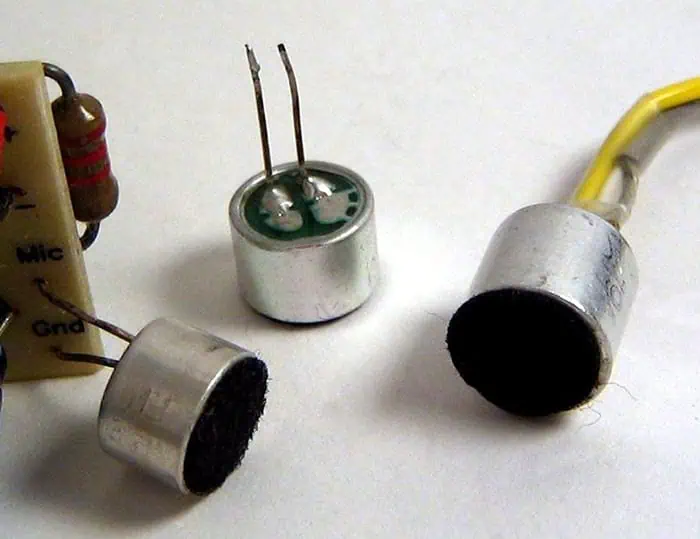
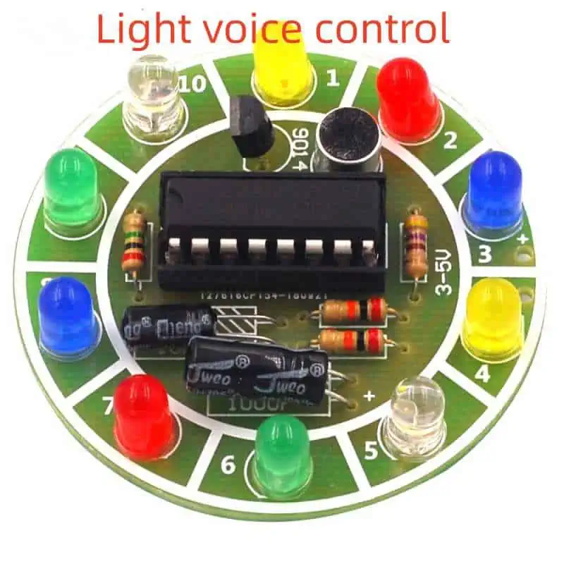
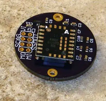
The shape of the common electret microphone is divided into two types: the built-in type and the external type.
Machine-mounted electret microphones are suitable for installation in a variety of electronic devices. The common machine-mounted electret microphones are mostly cylindrical in shape, and their diameters are φ6mm, φ9.7mm, φ10mm, φ10.5mm, φ11.5mm, φ12mm, φ13mm, and the pin electrodes are divided into two ends.
There are two types of three-terminal type, the lead type of the lead-in type with the soft-shielded wire and the lead-type type without the lead wire which can be directly soldered on the circuit board. If classified by volume, there are two types: normal type and miniature type.
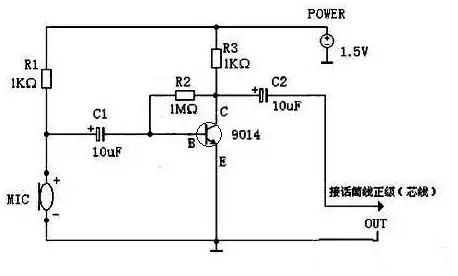
The resistor R1 is responsible for supplying the working voltage to the microphone, R2 and R3 are responsible for providing the bias voltage to the tertiary tube, and the capacitor C1 is responsible for coupling the signal of the microphone to the tertiary tube 9014 for amplification, and finally the amplified signal is coupled through the capacitor C2. Returned to the positive level of the microphone line.
9014 has the following magnification levels: A=60-150 B=100-300 C=200-600
(-9014 C 998 used here) D=400-1000
After the QQ chat test, the sound quality is clear and there is no noise. And in a 13 square meter room, there is no problem talking to the microphone one meter. Most importantly, a typical seventh battery can also be powered continuously for several months. The circuit is simple and the parts are few, which provides a good method for the friends with small microphone sound. After the speech is not so tired, the other party can hear clearly.
Soldering is a critical process used to mechanically and electrically join components in electronic assemblies. Insufficient solder can lead to poor quality solder joints that are unreliable both electrically and mechanically. There are several potential causes that can result in insufficient solder during the soldering process:
Poor Solderability of Parts
The solderability refers to how well the parts to be soldered can wet and adhere to solder. Following factors affect solderability:
Oxidation or Contamination
Metal surfaces like component leads and PCB pads get oxidized over time
This makes solder wetting difficult resulting in poor joints
Oil, grease or other residues also reduce solderability
Incompatible Materials
Certain metals like stainless steel and aluminum do not solder well
Lead-free solders have worse solderability than leaded solders
Mismatch between surfaces and solder alloy reduces wetting
Old Components
Components stored for long periods have degraded solderability
Moisture absorption also reduces solderability of parts
Lack of Solder Coating
Components without pre-applied solder coating have poorer solderability
Outgassing and drying of the paste deposit before reflow
Slumping of paste due to high ambient temperatures
Good process controls, stencil cleaning, monitoring of paste deposits and proper storage helps avoid these issues.
Defects in PCB and Component
PCB and component defects that absorb solder and restrict flow result in insufficient solder:
PCB Defects
Voids in ground or thermal planes acting as heat sinks
Poor pad design with insufficient wetting area
Contamination like oils and residues on pads
Component Defects
Cross-talk barriers blocking flow between leads
Tight lead spacing preventing access to solder
Warped leads or gaps between lead and PCB pad
Inspecting PCBs and components and checking pad dimensions ensures such issues are avoided.
Inadequate Flux
Flux removes surface oxides enabling solder flow and wetting. Following flux related reasons reduce soldering effectiveness:
Too little flux applied to joint
Flux drying out before completing soldering
Weak or water-soluble flux that is too mild
Low activity of aged flux reducing cleaning capability
Baked on or burnt flux residues interfering with wetting
Adequate amount of appropriate rosin-based flux should be applied to maintain solderability.
Problems with Solder Wire
Issues with solder wire composition and condition also affect soldering:
Impurities and voids in solder wire reducing fluidity -Insufficient wire diameter to thermal mass of joint
Oxidation or contamination of solder wire surface
Mismatch between alloy melting point and process temperature
Low tin-lead percentage of alloy increasing melting point
Proper solder wire handling and selection compatible with process requirements avoids these problems.
Other Process Issues
Excessive heat sinking due to large ground planes
Jigging misalignment resulting in loss of contact between tipped iron and joint
Soldering for too short a duration to allow adequate heating
Vibration or movement disturbing solder bead formation
Poor fume extraction exposing joints to corrosive flux residues
Control and monitoring of process parameters is needed to counteract these effects.
Troubleshooting Insufficient Solder
Visually inspect joint closely under magnification to identify poor wetting, cold spots etc.
Use solderability testing chemicals like rosin that react when applied to oxidized/contaminated areas
Thermally profile temperatures at joint during soldering to check if adequate temperature is reached
Review process parameters like heat application duration, wire gauge, tip size etc.
Evaluate PCB design – thermal planes, pad dimensions, spacing etc.
Test flux activity and assess paste condition
Check for issues with solder bath contamination or dross buildup if wave soldering
Preventing Insufficient Solder
Use proper storage and handling of components to maintain solderability
Apply solderability preservatives like benzotriazole on surfaces
Ensure PCB and component cleanliness before soldering
Select the right solder alloy matched to process temperature
Use adequate flux and apply uniformly to joints
Clean and tin soldering iron tips regularly
Optimize soldering temperature, duration and motion
Inspect stencil condition and paste deposits
Ensure adequate fillet wicking over joint
Monitor the soldering process continuously and make adjustments as needed
With proper analysis of root causes and preventive steps, issues due to insufficient solder can be eliminated resulting in reliable, high quality solder joints.
FAQs
Q1. How can I identify if insufficient solder is causing poor quality joints?
Look closely under magnification for joints with dull finish, grainy structure, dark spots, non-wetting and dewetting of surfaces indicating cold solder. Probe joints for continuity issues signalling poor bonding.
Q2. What is the ideal temperature for hand soldering with lead-tin alloy?
For Sn60Pb40 solder, ideal tip temperature is around 370℃ to 400℃. Higher temperatures above 450℃ should be avoided to prevent damage to components.
Q3. How does excess flux cause insufficient solder problems?
Too much flux can actually impede solder flow rather than helping it. It also leads to charring which deposits residues that hinder wetting. A thin uniform layer of flux should be applied.
Q4. Can inadequate solder volume be a reason for insufficient solder defects?
Yes, using too little solder wire compared to the thermal mass of the joint can lead to insufficient solder. Larger wire diameter or longer application time is required.
Q5. What is the effect of oxidation on solderability?
Metal oxide formation on surfaces interferes with solder wetting by creating a barrier layer. Flux helps remove oxides but preventing oxidation via protective coatings or oxidation inhibitors also improves solderability.
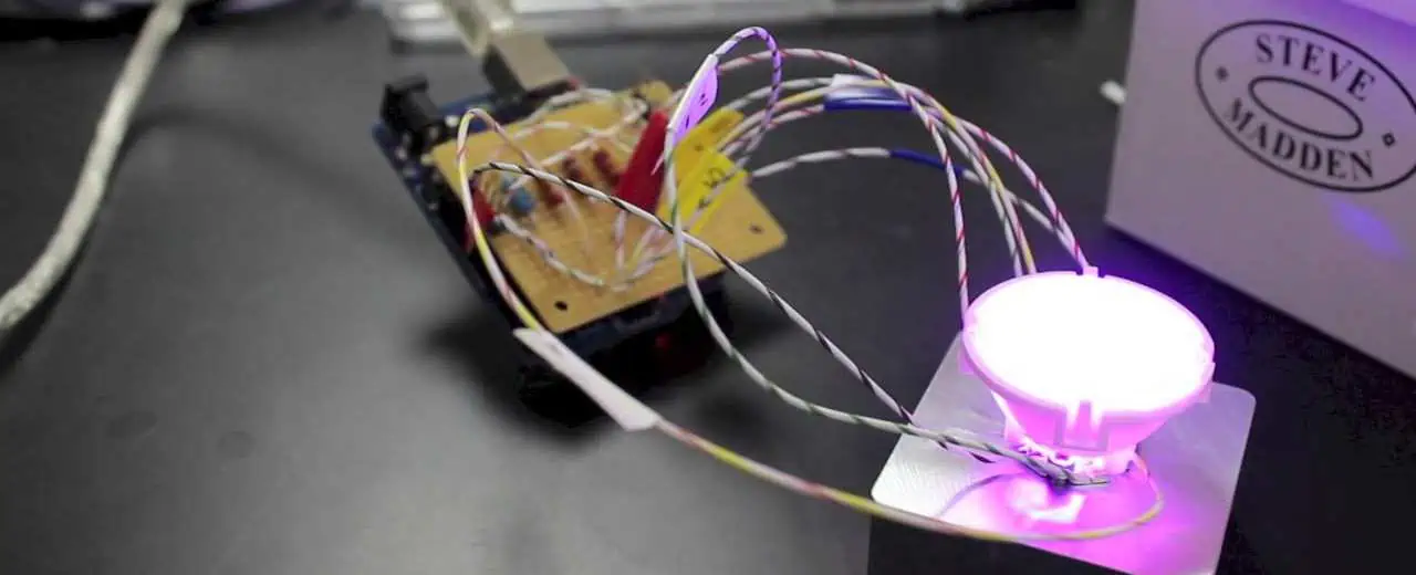
Voice controlled devices are becoming increasingly popular in home automation and assistive applications. The ability to control lights and other appliances simply by voice commands offers great convenience and accessibility. This article provides a step-by-step guide on designing a voice activated light system using modern speech recognition modules and microcontroller boards.
Key stages in the design process including selection of components, circuit design, power supply, programming and testing will be covered. Additionally, tips to enhance the performance, range and capabilities of the system are provided. The article concludes with a FAQ section on common queries regarding voice controlled lights.
System Overview
A block diagram of the voice activated lights system is shown below:
The major subsystems are:
Voice Recognition Module – Detects speech commands and converts to electrical signals.
Microcontroller – Processes signals from voice module and controls light switching circuitry.
Load Driver – Switches lights ON/OFF based on microcontroller output.
Power Supply – Provides regulated power to the circuits.
Some useful applications of this voice controlled lighting system:
Assistive device – Help disabled or elderly people control lights independently
Hands-free control – Enable light switching when hands are occupied
Energy savings – Lights left on accidentally can be turned off by voice
Smart home automation – Control various appliances, not just lights by voice
Industrial environments – Allow control without removing gloves or PPE
Conclusion
In this article, a step-by-step guide to designing a DIY voice activated light system was provided. The key components of voice recognition module, microcontroller, load drivers and power supply were selected. The complete circuit schematic, power supply, Arduino code and testing techniques were elaborated. Additional tips were provided to extend the functionality and applications of voice controlled lights. The information provided serves as a practical blueprint for hobbyists, students or designers to build their own customized voice activated lighting solutions.
FAQs
Q1. Can you use a sound sensor instead of voice recognition module?
Sound sensors like condenser mic modules are cheaper but detect all sounds rather than specific voice commands. So they are not as effective for selective voice control.
Q2. Is WiFi required for voice activated lights?
No, WiFi is not required. The voice recognition, lights control and switching are all handled locally using standalone hardware modules. But WiFi can be added optionally for remote control.
Q3. How many lights can be controlled by this system?
The number of lights depends on the power rating of the load driver circuitry used. For the Arduino and MOSFET based design, up to 50-100W of LED lighting can be controlled in most cases.
Q4. Does the microphone need to be near the person?
The microphone should be placed appropriately to clearly receive commands. Lapel microphones or external mics can be used so users do not have to be very close.
Q5. Can you add an automatic shut off timer?
Yes, the Arduino code can be modified to turn the lights off automatically after a preset duration to save energy using a timer variable and the millis() function.
Modern automobiles are packed with sensors to monitor the various systems and provide critical signals to the engine control unit (ECU). But the raw sensor outputs cannot be directly used by the ECU and need proper signal conditioning to make them usable for control and diagnostics. Signal conditioners play a vital role in interfacing the wide variety of sensors to the ECU in the harsh electrical and environmental conditions seen in automotive applications.
This article provides an overview of the different types of sensor signal conditioning circuits used in automobiles and their importance in sensor interfacing. Key design considerations and implementation methods are also discussed.
Automotive Sensors Overview
Some major sensors used in automobiles along with sensed parameter and typical output:
This demonstrates the wide variety of sensor signals the ECU has to process – analog voltages, digital pulses, variable resistance. The signals need to be conditioned before they can be digitized by ECU analog to digital converters (ADCs) and used in control algorithms.
Need for Signal Conditioning
The key functions of sensor signal conditioners are:
Gain – Boost weak sensor outputs to improve signal to noise ratio and match ADC input range.
Filtering – Remove out-of-band noise that can cause errors. Anti-aliasing filter for ADCs.
Linearization – Convert non-linear sensor responses to linear format for simplicity.
Impedance Conversion – Alter sensor output impedance to prevent loading effects.
Isolation – Protect ECU from transients and abnormal sensor voltages.
Excitation – Provide stable voltage/current to passive sensors like thermistors.
Compensation – Counteract sensor inaccuracies like shift over temperature.
Standardization – Present sensor data in normalized formats like 0-5V irrespective of sensor type.
Proper signal conditioning is vital for the ECU to get clean, accurate data from the sensors in the harsh, noisy on-vehicle environment. It acts as the interface between sensors and ECU ADC.
Sensor Signal Conditioner Architectures
Sensor signal conditioners can be implemented in different ways:
Discrete Conditioners – Use op-amps, discrete passives on PCBs. High flexibility but large size.
Integrated Circuits – Special ICs tailored for common functions like amplification, filtering. Compact but limited configurability.
FPAAs – Field Programmable Analog Arrays allow reconfiguration of signal chain. Good tradeoff between size and flexibility.
Module Based – Complete sensor interfacing on a module or board including ADC. Medium flexibility and size.
SoC Based – Sensors, signal chain and ADC integrated on a single chip. Highest integration but custom development needed.
Selection depends on size constraints, development cost and customization needs. Module based conditioning provides a good balance and reduces development effort.
Common Conditioning Circuits
Some typical conditioning circuits used with major automotive sensor types are discussed next:
Bridge Sensors
Load cells, strain gauges use a Wheatstone bridge structure. A basic bridge circuit completes the bridge and amplifies the differential output voltage:
The differential gain rejects common mode noises. Adjustable potentiometers are provided for calibration. The amplified output represents the sensed parameter.
Thermistors
NTC thermistors exhibit large resistance changes with temperature. A potential divider topology can convert this to a voltage:
The voltage varies non-linearly with temperature. Linearization using the Steinhart-Hart equation embedded in the ECU firmware gives accurate temperature.
Digital Hall Sensors
Hall effect position sensors like throttle position sensors have a digital PWM output whose duty cycle varies with position. An integrating filter converts this to an analog voltage:
The RC filter integrates the PWM signal to analog. The diode clamps negative cycles. Result is a clean 0-5V varying with position.
Piezoresistive Pressure Sensors
Sensors like the manifold absolute pressure (MAP) sensor use a Wheatstone bridge piezoresistive structure to detect intake pressure. Similar to bridge sensors, a differential amplifier conditions the output:
Differential gain boosts small mV level signals to 0-5V range. Adjustable potentiometers used for calibration.
Capacitive Position Sensors
Non-contacting capacitive position sensors have a variable capacitance output depending on shaft position. It forms part of an RC oscillator:
The oscillator frequency varies with capacitance change, which is demodulated to a analog voltage representing position by using a PLL, counter or ADC frequency measurement.
Magnetic Wheel Speed Sensors
Active wheel speed sensors produce a square wave frequency directly proportional to the wheel speed:
Signal is buffered via a comparator to clean it up before sending to ECU counter input. No analog conditioning required since sensor output is digital pulse train.
Current Loop Sensors
Some sensors like MAF output a current proportional to intake air mass flow rate and require a simple resistor to convert to voltage:
A low value sense resistor converts the 4-20 mA current to a 0-5V voltage for the ECU ADC. Care taken to ensure voltage burden does not affect sensor performance.
Design Considerations
Some key points considered during design of sensor signal conditioning circuits:
Sensor output characteristics – magnitude, impedance, linearity, frequency response, etc.
Noise and interference – EMI, crosstalk, engine electrical noise, etc.
Tolerance to environmental stresses – temperature, vibration, humidity
Fail safe provisions – defaults to known state upon failure
Effect on sensor function – biasing, loading, source impedance, feedback etc.
Diagnostics capability – able to detect open/short sensor faults
Protection – prevent damage to ECU from overvoltage and transients
Performance over supply voltage and temperature range
Cost, size and design effort constraints
Simulations, prototyping and testing ensures the conditioning circuits provide clean, accurate, normalized sensor data to the ECU under all on-vehicle conditions.
Implementation Methods
There are different approaches to implement the sensor signal conditioning circuits:
Discrete – Using separate opamps, discrete resistors, capacitors
Allows precision conditioning but large size, assembly effort
Reconfigurable signal chain blocks for decent flexibility
Module Based – Complete circuit on a dedicated PCB module
Self-contained, quick to integrate but moderate flexibility
SoC – Integrated sensor, signal chain and ADC in a single IC
Maximum integration but fully custom mixed-signal IC development needed
Software Based – Digitize raw sensor output and use software algorithms
Configurable but latency, noise can affect control performance
A module-based approach provides a good tradeoff – easy integration with conditioning tailored for each sensor for automotive production use.
Testing and Calibration
Thorough testing of sensor conditioning electronics is needed to ensure proper operation under all conditions:
Functionality Testing – Validates circuit operation over temperature and voltage ranges with known simulated sensor inputs.
Noise Testing – Quantifies noise and distortion levels introduced by the conditioning circuits.
Error Budgeting – Calculates overall system error by considering all component tolerances, drifts and nonlinearities.
Fault Testing – Verifies fail safe behaviors upon open, short or out of range sensor inputs.
Calibration – Potentiometers, digital trims are adjusted based on calibration with sensor reference standards to minimize errors.
Lifetime Testing – Assesses performance degradation due to thermal cycling, vibration, humidity and aging effects. Confirms adequate service lifetime.
The signal conditioning circuits are a vital link between sensors and ECU. Proper design and testing ensures the ECU gets accurate, noise-free data from the wide variety of sensors in the harsh on-vehicle environment over the vehicle’s lifetime. This enables advanced engine management, fuel efficiency, diagnostics and safety features.
Conclusion
An overview of the common signal conditioning methods used with major automotive sensor types has been presented. Discrete circuits based on opamps, integrated amplifier ICs, FPAAs and module based approaches provide flexible solutions for the varying needs of different sensors while meeting challenges like noise, nonlinearities etc. When designed keeping in mind sensor characteristics, environmental conditions, ECU interface requirements and performance constraints, the sensor conditioners reliably acquire and process raw sensor signals into the standardized, accurate data needed by ECUs for precise engine control. Advancements in programmable mixed-signal ICs and miniaturization will enable higher levels of integration and intelligence in sensor interfaces, moving towards more accurate and responsive engine control systems.
Automotive Sensor Conditioners – FAQs
Q1. How does signal conditioning help the ECU analyze sensor data?
Signal conditioning transforms the raw sensor output into a clean, standard format required by ECU ADC and algorithms – amplifying, linearizing, protecting from transients/noise, converting impedance/format etc. This enables accurate measurement.
Q2. What are some important specifications for automotive sensor signal conditioners?
Key parameters are bandwidth, linearity, stability, drift, noise performance, fault tolerance, protection rating, size/weight, reliability, EMI/EMC compliance, temperature range, input/output impedances and flexibility.
Q3. Which type of sensor interface circuit is most suitable for wheel speed sensors?
Wheel speed sensors output a digital pulse train whose frequency is proportional to speed. Only buffering is needed so a basic comparator circuit provides the required conditioning to clean up pulses before input to ECU counter.
Q4. How can capacitive type position sensors be interfaced to an ECU?
The capacitance versus position characteristic can be converted to a frequency using a capacitance-to-frequency converter circuit. The frequency can then be measured digitally by the ECU using a timer input to determine position.
Q5. What are some methods used for linearizing thermistor response vs temperature?
Using microcontroller algorithms to implement mathematical linearization models like Steinhart–Hart model or look-up tables. Analog linearization circuits using resistor networks or diodes to counteract the thermistor nonlinearity.
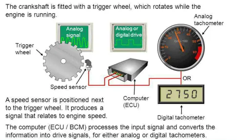
A wide range of instantaneous speed measurement accuracy of high speed sensor Schematic diagram.
A speed sensor is a sensor that converts the speed of a rotating object into a power output.
The speed sensor is an indirect measuring device that can be manufactured by mechanical, electrical, magnetic, optical and hybrid methods. According to the different signal form, the speed sensor can be divided into analog and digital, sample as below:
The output signal value of the analog speed sensor is a linear function of the rotational speed, and the output signal frequency of the digital speed sensor is proportional to the rotational speed, or its signal peak interval is inversely proportional to the rotational speed.
The wide variety and wide range of speed sensors is due to the extensive use of a wide range of motors in automatic control systems and automation instrumentation, and strict requirements for accurate measurements of low speeds (such as one turn per hour), high speeds (such as hundreds of thousands of revolutions per minute), steady speeds (such as errors only) and instantaneous velocities in a number of situations. The commonly used speed sensor has photoelectric type, capacitance type, variable reluctance type and speed measuring generator and so on.
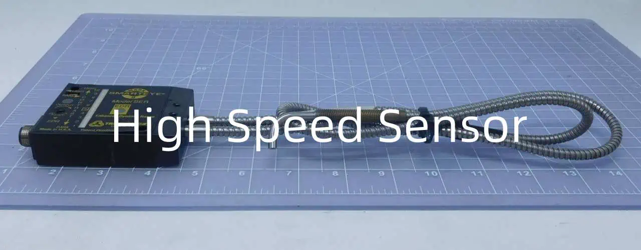
A high speed sensor is a type of transducer that can detect and measure high speed motion, vibration or rotation and convert it into an electrical signal for data acquisition and analysis. High speed refers to frequencies above 10 kHz in most applications. These sensors play a vital role in studying high frequency dynamic phenomena in fields like structural health monitoring, machine condition monitoring, automotive industry, avionics etc. The high sampling rate is necessary to capture enough data points for accurate detection and measurement.
Some common applications of high speed sensors include:
Vibration and modal analysis of structures like buildings, bridges, aircraft wings etc.
Monitoring blade tip deflections in gas turbine engines of jet aircraft.
Engine knocking detection in automotive engines.
Monitoring machine tool vibration in manufacturing industry.
Studying effects of explosions and impacts.
Monitoring pressure fluctuations in fluid flow systems.
Studying acoustic emissions in materials.
This article provides an overview of different types of high speed sensors, their working principles, key specifications, instrumentation for high speed data acquisition and analysis. Circuit schematics are also included for common sensor interfaces.
Types of High Speed Sensors
Some common types of sensors used for high frequency measurements and their typical frequency ranges are given below:
Accelerometers
They measure acceleration and vibration. Useful frequency range – 0 Hz to over 50 kHz. Common technologies:
Measure displacement and position directly. Useful frequency range – 0 Hz to 20 kHz. Common types:
LVDT – Up to 2 kHz
Eddy current sensors – Up to 10 kHz
Capacitive and inductive sensors – Up to 50 kHz
Pressure sensors
Measure dynamic pressure. Useful frequency range – 0 Hz to >100 kHz. Types:
Piezoelectric dynamic pressure sensors
Fiber optic sensors – Up to 100 kHz
Force sensors
Measure dynamic force. Useful frequency range – 0 Hz to 50 kHz. Common types:
Piezoelectric load washers – Up to 30 kHz
Strain gage load cells – Up to 5 kHz
Motion encoders
Measure speed, position, rotation angle. Useful frequency range – 0 Hz to 50 kHz. Types:
Optical incremental encoders – Up to 50 kHz
Magnetic encoders – Up to 10 kHz
Acoustic emission sensors
Measure high frequency stress waves. Useful frequency range – 20 kHz to 1 MHz. Types:
Piezoelectric sensors
Fiber optic acoustic sensors
High Speed Sensor Specifications
Some key specifications of high speed sensors are:
Frequency response – The sensor should have a flat frequency response over the measurement bandwidth.
Sensitivity – Amount of electrical signal output per unit of measured parameter. Higher sensitivity allows resolving smaller signals.
Resolution – Smallest detectable change in the measured quantity.
Dynamic range – Ratio of the maximum to minimum measurable quantity. Wider dynamic range allows measuring both small and large signals.
Phase response – Minor deviations from the ideal 0° or 180° phase are acceptable. Large phase errors make data analysis difficult.
Noise – Should be low for resolving small signals. Critical for high resolution measurements.
Non-linearity – The output should have a linear relationship with the input. Non-linearity causes measurement errors.
Crosstalk – Signals from one axis should not affect other axes. Important for multi-axis measurements.
Temperature range – Sensor should perform well over required operating temperature range.
Size and weight – Important if sensor has to be mounted on structures which have weight and space constraints.
Instrumentation for High Speed Data Acquisition
The sensor output has to be captured by appropriate data acquisition hardware for analysis. Important parameters:
Sampling rate – Must be high enough to avoid aliased spectra according to Nyquist criteria. For frequencies up to 50 kHz, 1 MHz sampling rate is usually sufficient.
Resolution – Analog to digital converter (ADC) resolution between 16 to 24 bits preferred. Lower resolution limits dynamic range.
Bandwidth – Data acquisition system analog bandwidth must be higher than maximum sensor frequency.
Number of channels – Important if using multiple sensors for modal testing, NVH testing etc. 8, 16, 32 channels systems common.
Signal conditioning – Amplification, filtering required to match sensor output to ADC input range.
Antialiasing filter – Low pass filter before ADC to prevent aliasing.
Data transfer speed – Must be fast enough to stream data to processor memory from high sampling rates.
Triggering – Required to start data capture at specific events. Important for transient events like impacts.
Data acquisition software – Manages hardware settings, data streaming, storage and analysis features.
High Speed Sensor Interfacing Circuits
Some common sensor interfacing circuits are shown below:
ICP Accelerometer Interface
ICP (Integrated Circuit Piezoelectric) accelerometers require constant current excitation for proper functioning. The ICP sensor conditioner provides 2-20 mA constant current and converts the sensor output voltage to a low impedance voltage proportional to acceleration. The low pass filter removes frequencies above the sensor range. The amplifier gain is set to match the ADC input range.
AC-Coupled Accelerometer Interface
AC coupled interface is suitable for accelerometers with voltage mode output. The high pass filter blocks the DC component and provides the AC acceleration signal centered around 0V. The gain stage amplifies the signal to match the ADC input range.
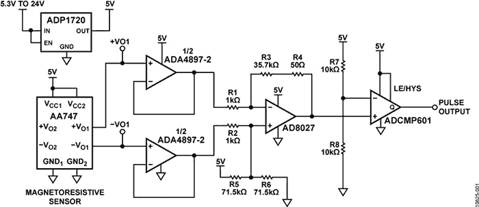
Differential Velocity Sensor Interface
Geophone velocity sensors have a differential coil output. An instrumentation amplifier converts this to a single ended low impedance voltage for digitization. The amplifier gain is set based on the geophone sensitivity and ADC input range.
Bridge Sensor Interface
Strain gages, load cells etc. have Wheatstone bridge type outputs. A bridge completion resistor converts this to a differential voltage input for the instrumentation amplifier. The amplifier gain calibrates the output to engineering units like force, acceleration etc.
Potentiometric Displacement Sensor Interface
Potentiometric displacement sensors like LVDTs have a voltage divider output proportional to position. A difference amplifier converts this to a single ended low impedance output representing the displacement. Excitation voltage must match LVDT specifications.
Digital Encoder Interface
Digital incremental encoders provide quadrature TTL/CMOS pulse outputs for position and speed sensing. A high speed counter chip captures and processes the pulses to give position data. The counter resolution and speed determine the measurement resolution.
High Speed Data Analysis
The captured time domain sensor data is processed using digital signal processing techniques for relevant frequency and time-frequency domain information.
Time Domain Analysis
Analysis in time domain involves:
Plotting sensor output vs. time
Statistical measures like RMS, peak, crest factor etc.
Time waveform parameters like rise time, overshoot, settling time
Time domain averaging for improving signal to noise ratio
Frequency Domain Analysis
Fourier Transform to get frequency spectrum
Analyze dominant frequencies
Compare vibration levels at different frequencies
Identify resonances
FFT spectrum averaging for reducing variance
Order analysis for rotational equipment
Time-Frequency Analysis
Short Time Fourier Transform (STFT)
Wavelet Transform
Understand non-stationary signal characteristics
Analyze transients and machine start-up data
Modal Analysis
Extract modal parameters like frequency, damping, mode shapes
Operational modal analysis techniques
Finite Element model correlation
Structural health monitoring
Proper sensor selection, instrumentation and analysis help gain valuable insights from high speed dynamic measurement data.
High Speed Motion Detection Techniques
Detection and measurement of high speed motion has applications in diverse fields including manufacturing, transportation, material testing, biomechanics and more. Some key techniques used for high speed motion detection are:
1. Laser Doppler Vibrometry
Non contact measurement using Doppler shift of reflected laser beam
Resolves nano and micron level vibrations up to 10 MHz speeds
Low noise, high frequency response
Measures displacement, velocity, acceleration
Used for MEMS devices, acoustic measurements etc.
2. Stroboscopic Video Motion Analysis
High speed video camera with stroboscopic illumination
Motion appears slowed down under strobed light
Allows visualization of fast periodic motion
High recording speeds up to 100,000 fps
Used for speaker diaphragm, rotating machinery motion analysis
3. Photon Doppler Velocimetry
Measures velocity by light scattered from moving particles in flow
Provides instantaneous whole field velocity distribution
Used extensively in fluid mechanics, combustion research
Velocities up to supersonic speeds measurable
4. Capacitive and Inductive Sensors
Non contact displacement measurement
High frequency response up to 100 kHz
High resolution and sensitivity
Small and compact for embedded applications
Used for proximity sensing, precision position control
5. Piezo Film Sensors
Thin piezoelectric polymer films used as sensors
Measure stress, strain, vibration, pressure
Broad frequency range up to 1 MHz
Highly flexible, can be bonded/embedded
Used for acoustic emission, structural health monitoring
6. MEMS Inertial Sensors
MEMS accelerometers, gyroscopes for motion sensing
Detect acceleration, angular rate, vibration
High bandwidths up to 50 kHz
Low cost, small size
Used in IMUs, condition monitoring, navigation
Proper selection of detection technique is key for successful high speed motion measurement and analysis.
Schematic Diagram of a High Speed Data Acquisition System
A typical high speed data acquisition system consists of sensors, signal conditioning, DAQ hardware, analysis software as shown in the schematic diagram:
The sensors transduce the high speed physical phenomenon into electrical signals. Different types of sensors can be used based on the quantity to be measured.
Signal conditioning circuits like amplifiers, filters provide gain, filtering, offset adjustment, common mode rejection etc. to match the sensor output to the DAQ input range.
High sampling rate DAQ device digitizes the conditioned analog signals via an antialiasing filter and ADC. Synchronized multi-channel capture is enabled by a common clock and trigger.
Data is transferred over high speed ports like USB, Ethernet to the analysis software on PC. Buffering helps prevent data loss.
Analysis software has capabilities for time domain waveform display, frequency spectra, order analysis, modal analysis etc. Report generation, data export facilities are included.
Proper schematic design is key for accurate acquisition of high frequency signals and extracting useful information through digital signal processing techniques.
Conclusion
High speed sensors and data acquisition systems enable detailed analysis of high frequency dynamic phenomena that cannot be captured using traditional sensors and DAQ devices. With recent advances, frequencies up to 1 MHz can be reliably measured using MEMS sensors, fiber optic sensors and compact DAQ devices.
Selection of appropriate sensors based on frequency range, operating conditions and output characteristics is vital. Suitable signal conditioning ensures the sensor output is correctly interfaced to the DAQ system. High sampling rates, resolution and bandwidths are essential to avoid aliasing and allow detection of small signals.
Powerful analysis software provides the tools to transform the captured time domain data into useful frequency, order and modal domain information through transforms, spectral analysis and other techniques. This high speed dynamic data is critical for condition monitoring, predictive maintenance, product design validation and other applications.
Frequently Asked Questions (FAQ) related to High Speed Sensors
Q1. What is the key difference between a high speed sensor and a regular sensor?
The main difference is the frequency response. High speed sensors can measure dynamic signals up to 100 kHz and beyond while regular sensors are limited to 1-10 kHz range. High speed sensors use specialized technologies to achieve the fast response required.
Q2. What sensors can I use for high frequency vibration measurement?
Piezoelectric, piezoresistive and MEMS accelerometers are commonly used for vibration measurement in 20 Hz to 50 kHz range. Accelerometers with resonant frequencies up to 500 kHz are available. Optical laser vibrometers can measure up to 10 MHz vibrations.
Q3. What instruments do I need for high speed sensor data capture and analysis?
You need a high sampling rate DAQ device – at least 200 kHz for mechanical vibration measurements. DAQ should have enough analog bandwidth, resolution (16 bits or more) and channels. Software is needed for signal processing, FFT analysis, order tracking etc.
Q4. How do I interface a sensor with voltage output to the DAQ system?
Use a conditioner circuit with gain and filter stages. The gain should amplify the sensor output to match the DAQ input range. Filter out frequencies above the sensor range. Provide excitation if required. Protect sensor from overvoltage.
Q5. Which technique can perform non-contact measurement of high speed periodic motion?
Stroboscopic video motion analysis is ideal for non-contact measurement of high speed periodic motion like speaker cones, fan blades, shafts etc. It uses high speed camera with strobed light source and allows viewing motion in slow motion.
Properly designing trace spacing and widths is critical when laying out printed circuit boards. Together, these parameters impact current carrying capacity, impedance, noise, manufacturability, and signal integrity. Insufficient spacing or improper trace widths can lead to short circuits, crosstalk, excessive EMI, and other issues degrading circuit performance.
This article provides guidance on how to select appropriate PCB trace spacing and widths based on current levels, voltage, impedance targets, noise minimization, and fabrication capabilities. Design examples along with spacing and width determination procedures are also provided.
Trace Spacing Basics
Trace spacing refers to the distance between adjacent PCB traces on a given layer. Key considerations when setting trace spacing include:
Isolation – Prevent short circuits between closely spaced high voltage traces.
Crosstalk – Minimize interference between neighboring traces, especially for fast switching digital or RF traces.
Impedance – Spacing impacts achievable trace impedance based on capacitive coupling.
Current – High current traces require larger spacings to prevent voltage arcing.
Manufacturability – Accommodate tolerances of fabrication processes.
Repairability – Provide adequate spacing for rework, solder mask repair, or trace cuts.
Routing Density – Tighter spacings allow greater layout density.
Balancing these considerations determines optimal trace-to-trace spacing.
Trace Width Basics
PCB Claculator Trace Width
Trace width is the cross-sectional width of a conductive copper track. Key factors influencing width selection include:
Current Rating – Wider widths increase current carrying capacity.
Accommodate fabrication process capabilities and tolerances:
PCB Technology
Minimum Spacing
>6 layer board
5 mils
2-6 layer board
6 mils
Doubleside board
8 mils
Thick copper boards
>10 mils
Safety Margin
Adding margin prevents shorts from process variability:
10-20% extra spacing for margin
More margin for prototyping vs production
Careful application of appropriate design rules ensures reliable trace isolation.
Trace Width Design Rules
Similar considerations guide trace width selection:
Based on Current
Wider traces allow higher current handling:
Trace Current
Minimum Width
< 0.5A
10mils
0.5A – 1A
15mils
1A – 2A
25mils
> 2A
40mils+
May need further widening based on thermal rise limits.
Based on Impedance
Narrower traces yield higher impedance:
Target Impedance
Trace Width
50 Ohms
5-15 mils
75 Ohms
6-25 mils
90-100 Ohms
4-10 mils
Based on Manufacturability
Match trace width to fabrication capabilities:
PCB Technology
Minimum Width
>6 layers
4 mils
2-6 layers
5 mils
Double sided
8 mils
Many factors determine optimal trace widths for reliable performance.
Variable Width Traces
reducing the trace and space size
Varying trace widths along a net’s length can optimize performance:
Taper traces from wider at source to narrower at destination to minimize reflections.
Neck-down before sensitive pins to control impedance. Flare-out after pins.
Minimize stubs and branches by tapering off rather than abruptly ending.
Use wider traces only where needed for higher current. Narrow elsewhere.
Size for voltage drop along route – wider where drop is excessive.
Choke points at junctions intentionally narrow traces to control impedance.
Intelligently varying widths enhances SI performance while optimizing utilitization of available space on the PCB.
Example Trace Width Calculations
Here is an example procedure to calculate a suitable trace width:
Step 1. Determine Required Current
Check electrical schematics to identify the maximum continuous or pulsed current through the trace (Imax). Margin by 10-20%.
Step 2. Determine Maximum Supported Current Density
The PCB laminate material sets a maximum limit on allowable amps/unit cross section area:
Standard FR4 is 200 mA/mil2
High current FR4 rated for 300 mA/mil2
IMS substrates handle 500-1000 mA/mil2
Step 3. Calculate Minimum Trace Width
Use the max current (Imax) and max current density (J) to determine minimum trace width:
Trace Width (mils) = Imax (A) / J (mA/mil2)
Add margin of 20% for reliability. Round up to nearest 5 mils.
Step 4. Verify Against Other Design Rules
Increase width if required by voltage spacing rules. Reduce if other constraints require thinner trace (impedance, thermal relief around pads, etc). Iterate as needed.
With this approach, appropriate widths meeting both electrical and physical needs can be derived.
Example Trace Spacing Calculations
Similarly, trace spacing can be determined analytically:
Step 1. Identify Maximum Voltage
Determine the highest voltage that will be present between the traces. Include fault conditions and margin.
Step 2. Set Spacing For Voltage Clearance
Use table of spacing-to-voltage ratios to choose a spacing that prevents arcing.
Step 3. Evaluate Based on Other Needs
Adjust for target impedance needs if traces are controlled impedance.
Check crosstalk limits for high speed traces.
Verify against any manufacturing minimum spacing rules.
Step 4. Add Safety Margin
Increase spacing from calculations above by 20% as a safety factor for process variability.
Using a structured approach ensures trace spacing and widths chosen meet both electrical and fabrication requirements for a robust, reliable PCB layout.
Summary
Trace spacing and width selection directly impact layout density, electrical performance, manufacturability and cost.
Selection determined by current levels, voltage, target impedance, crosstalk, process capabilities, and safety margins.
Design rules guide spacing and width based on isolation, impedance, noise, fabrication limits, and reliability.
Sophisticated layouts taper traces, vary widths on net spans, and control junction impedances.
Analytic calculations combined with design rule checks validate trace geometries for optimal PCB performance.
Carefully choosing trace widths and spacings is a key PCB layout skill necessary to balance myriad electrical and physical design constraints.
FAQ
How close can two traces be on a PCB?
The minimum spacing is set by voltage isolation needs and process capabilities. Traces under 50V can theoretically abut but at least 2x width spacing is recommended for margin. High voltage traces need much larger spacings.
How are trace widths measured?
Width is measured along the horizontal axis of the trace from soldermask edge to soldermask edge. The copper itself may be wider but spacing rules apply to mask-to-mask gaps.
Can track widths change on a single net?
Yes, tapering traces, widening only where needed, and impedance-controlling neck-downs allow optimization. However, abrupt changes in widths create impedance discontinuities and should be avoided.
What determines trace thickness on PCBs?
Copper thickness is generally fixed for a given PCB laminate and layer count. But wider traces inherently end up with more vertical copper thickness which aids current capacity through greater cross-sectional area.
How much spacing is needed between digital and analog traces?
A minimum of 3x-4x trace width separation is recommended, along with judicious use of ground planes. This prevents coupling noise from fast digital edges into sensitive analog nodes.
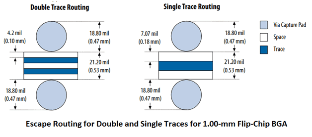
1. The signal circuit that needs to do impedance should be set strictly according to the circuit width and circuit spacing calculated by the pcb stack-up. For example, Radio frequency(RF) signal ( conventional 50R control), important single-ended 50R, differential 90R, differential 100R and other signal circuit, through the stack-up can calculate the specific circuit width circuit spacing (pictured below).
2. The circuit width and circuit spacing of the design should consider the production process capability of the selected PCB production factory. If the circuit width and circuit spacing are designed to exceed the process capability of the cooperating PCB manufacturer, it is light to add unnecessary production costs. It is serious that causes the design to fail to produce. Under normal circumstances, the circuit width is controlled to 6/6mil, and the via is 12mil (0.3mm). Basically, more than 80% of PCB manufacturers can produce it with the lowest cost.
The circuit width is controlled to a minimum of 4/4mil, and the via is 8mil (0.2mm). Basically, more than 70% of PCB manufacturers can produce it, but the price is slightly more expensive than the first case, not too expensive. The circuit width is controlled to a minimum of 3.5/3.5mil, and the via is 8mil (0.2mm). At this time, some PCB manufacturers can’t produce it, and the price will be more expensive. The circuit width is controlled to a minimum of 2/2mil, and the via is 4mil (0.1mm, which is usually a HDI blind buried hole design, which requires laser via).
At this time, most PCB manufacturers can’t produce the price, which is the most expensive. of. The circuit width circuit spacing here refers to the size between the circuit to the hole, the circuit to the circuit, the circuit to the pad, the circuit to the via, the hole to the pad and something like that.
3. Set the rules to consider the design bottlenecks in the design file. If there is a 1mm BGA chip, the pin depth is shallow, only one signal circuit needs to be taken between the two rows of pins, which can be set 6/6mil, the depth of the pin is deep, and two pins need to be taken between the two rows of pins. The signal line is set to 4/4mil; there is a 0.65mm BGA chip, which is generally set to 4/4mil;There is a 0.5mm BGA chip, the minimum circuit width must be set to 3.5/3.5mil; the 0.4mm BGA chip generally needs to be HDI design. Generally, for the design bottleneck,
the area rule can be set (for the setting method, see the end of the article [AD software setting ROOM, ALLEGRO software setting area rule]), the local circuit width is set to a small point, and the other rules of the PCB are set larger for production. Improve the PCB pass rate.
4. We need to be set according to the density of the PCB design, the density is small, the board is loose, the circuit width can be set larger, and vice versa. General can be set by the following steps:
1) 8/8 mil, 12 mil (0.3 mm) via.
2) 6/6mil,12mil(0.3mm)via。
3) 4/4 mil, 8 mil (0.2 mm) via.
4) 3.5/3.5 mil, 8 mil (0.2 mm) via.
5) 3.5/3.5 mil, 4 mil (0.1 mm, laser perforation) for via.
6) 2/2 mil, 4 mil (0.1 mm, laser perforation) for via.
Maintaining controlled impedances on flexible printed circuit boards (flex PCBs) is critical for high frequency applications like RF circuits, high speed networking, automated testers, and medical imaging equipment. The challenges of variable dielectric thickness, dynamic bending, and conductor adhesion require special modeling and fabrication methods to achieve consistent impedances.
This article provides an overview of techniques to design and manufacture controlled impedance flexible circuits to ensure signal integrity and maximize performance.
Impedance Control Importance
Properly controlling impedance on flex PCBs provides several benefits:
Minimizes signal reflections that cause noise and interference
Allows matching with drivers, transmission lines, and receivers
Enables high frequency performance beyond just physical flexibility
Optimizes power transfer and efficiency up to microwave frequencies
Flex PCBs without impedance control should be limited to low frequency analog or digital signals below 10-20MHz that are more tolerant to impedance mismatches and reflections.
Accurate modeling of impedance on flex PCBs considers:
Thin, variable dielectric thickness
Lack of solid reference plane
Impact of bends/folds on dielectric spacing
Deformation when bent that changes spacing
Varying conductor width and profile
Common modeling approaches include:
2D Field Solvers
Most PCB modeling tools rely on 2D field solvers. Requires detailed cross-section definition considering bending, spacing, dielectric properties, and adhesive thicknesses. Provides good correlation to actual flex impedance with proper inputs.
3D Electromagnetic Solvers
Full 3D EM solvers offer the highest accuracy by modeling complex effects of bending, dielectric variations, and component placement. The computational requirements limit applications to smaller flex regions.
Lumped Element Models
A lumped parameter model approximates the distributed transmission line as discrete inductive, capacitive, and resistive elements. Quicker computations but reduced accuracy. Useful for initial estimates.
Validation Prototypes
Building controlled impedance test coupons allows empirical measurement and refinement of the models. This tuning of the simulation tools improves correlation and accuracy.
Developing accurate models requires careful attention to all physical construction details of the flex laminate materials and stackup.
Flex Stackup Design
Key considerations when developing the flexible PCB stackup include:
Select flexible laminate materials with tight impedance tolerances and stability over bending.
Minimize number of laminate layers which makes modeling easier.
Add reference planes wherever feasible to provide low impedance AC return paths.
Maintain symmetry between layer dielectric materials and thicknesses.
Use thicker copper layers to reduce resistive losses. 1oz baseline with 2oz in high current areas.
Model effects of solder mask thickness on impedance.
Ensure good registration between layers to prevent variations.
An optimized stackup minimizes the variability of parameters impacting impedance as circuits flex during use.
Trace Geometry Planning
With the stackup defined, transmission line trace geometry can be selected:
Choose initial trace width based on target impedance, typically between 100-250μm for 50Ω.
Ensure sufficient insulation clearance around traces based on voltage.
Use thicker traces than rigid PCBs due to greater roughness.
Increase spacing between adjacent traces to control coupling.
Minimize number of tight bend angles which cause impedance spikes.
Simulation of actual circuit trace geometry with the defined stackup provides the route to optimizing widths and spacings to hit target impedances.
Maintaining Impedance Under Bending
Special considerations help maintain consistency when flexed:
Model effects of dynamic bending and folding during use to quantify impedance deviations.
Limit the minimum bend radius to reduce impedance variations and conductor strain.
Use thinner laminate materials to provide better flexibility without deforming spacing and dielectric thickness.
Select laminate materials with elasticity to return to uniform spacing after bending.
Increase spacing between conductors to compensate for thickness changes under bend stress.
Understanding impedance variability under bending through modeling, material selection, and design allows mitigating changes when circuits are flexed in actual use.
Manufacturing Processes for Controlled Impedance
Fabrication processes must be optimized for impedance tolerances:
Surface preparation to remove oxides and promote polymer adhesion
Etch processes tuned to achieve precise trace geometry and minimize undercuts
Registration between layers of +/- 0.05mm or better
Symmetrical bond and lamination pressures to maintain dielectric spacing
Modeling and measuring impedance under dynamic bending improves reliability.
With robust design-manufacturing coordination, flexible PCBs can deliver controlled impedances.
Following comprehensive guidelines allows developing flex PCBs with the impedance control needed for mission-critical and high frequency applications.
FAQ
How much does bending decrease the impedance on flex PCBs?
Typical drop is 10-25% when flexed to moderate bend radii. Sharp, tight bends can reduce impedance by over 50% in extreme cases. The effect worsens with thinner flex materials.
Does solder mask thickness impact impedance on flex circuits?
Yes, variability in solder mask thickness and its proximity to traces impacts the capacitance to ground, affecting impedance. Keeping thickness uniform through tight process control is important.
Can flex PCBs use microstrips instead of striplines?
Yes, but a microstrip construction lacks a controlled reference plane and is more susceptible to bending variations. A stripline provides the most consistent impedance under dynamic flexing.
Are there impedance test points on flex PCBs?
Test coupons containing impedance measurement points are often included in the fabrication panel. This allows characterization and correlation to modeling predictions.
How often should controlled impedance models be updated?
Models should be refined based on measured results every 6-12 months. This compensates for any process changes over time. More frequent updates are recommended when first characterizing.
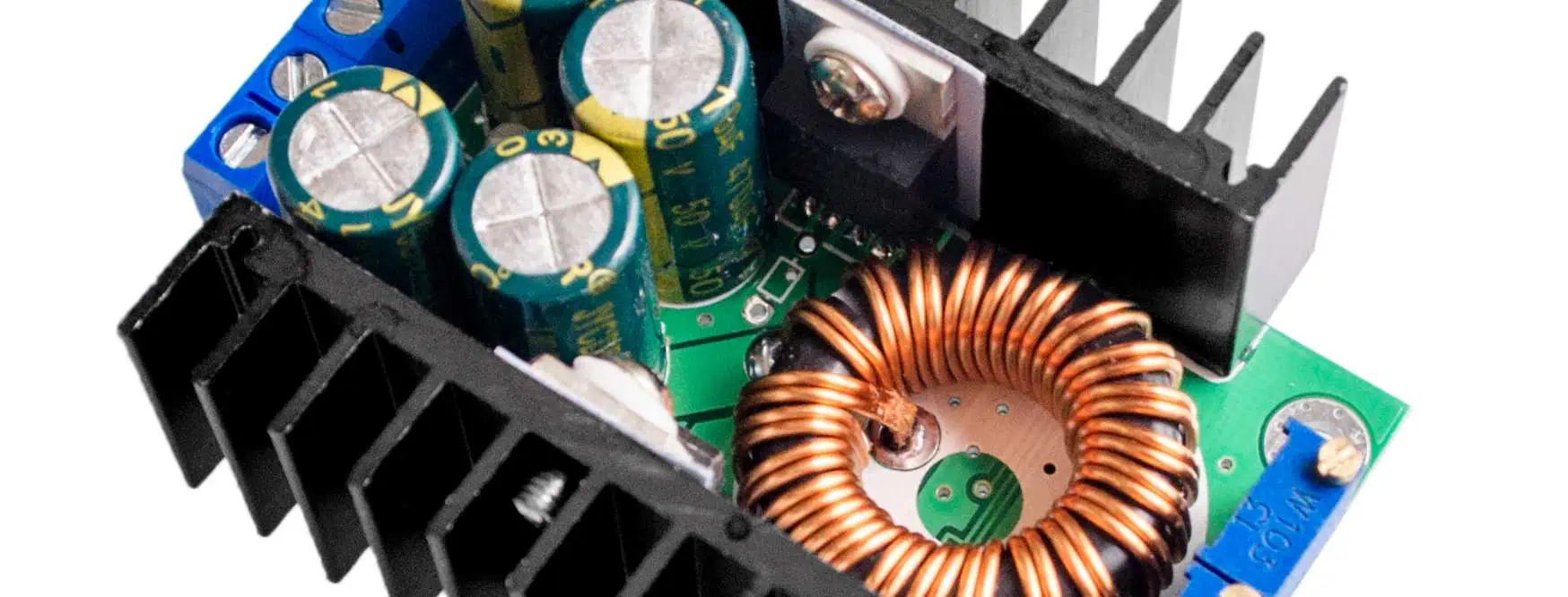
The working principle of the LED driver is to limit the maximum operating current by using the capacitive reactance generated by the capacitor at a certain AC signal frequency. Therefore, the working principle of the capacitor step-down is not complicated.
At 50Hz, the capacitance generated by a 1uF capacitor is about 3180 Ω.
When the AC voltage of 220V is added to both ends of the capacitor, the maximum current flowing through the capacitor is approximately 70mA.Although the current flowing through the capacitor is 70mA, but does not produce power consumption on the capacitor, if the capacitor is an ideal capacitor, then the current flowing through the capacitor is a virtual current, and its work is reactive power.
The use of capacitive buck schematic diagram is a common small current power supply diagram , with small volume,low cost and current is relatively constant and other advantages, and is also commonly used in the driving diagram of the LED.
The following figure shows an actual LED driver diagram with capacitor step-down: Most of the application diagram do not have a varistor or transient voltage suppression transistor. It is recommended that the connection, due to varistor or transient voltage suppression transistor can effectively discharge the mutation current in the moment of voltage mutation (such as led lightning, large power equipment start, etc.), effectively bleed the abrupt current to protect the diode and other transistors, and their response time is generally in the order of micro milliseconds.
The pressure resistance of the filter capacitor C2,C3 depends on the load voltage, which is generally 1.2 times times the load voltage, and its capacitance capacity depends on the size of the load current.
Introduction
Buck converters are DC-DC step down regulators that can provide an efficient and flexible means of driving LED lighting. By converting a higher DC input voltage to a lower adjustable output voltage, buck converters allow controlling the current through and brightness of LEDs.
However, LED loads present some specific design considerations for buck converter circuits regarding dimming methods, startup currents, and topology selections. With careful component selection and circuit configuration, buck regulators can form the basis of robust LED drivers that are compact, efficient, and inexpensive.
Buck Converter Basics
Here is a basic non-isolated buck converter circuit:
The key operating principles:
An inductor and capacitor connected in series smooths the switched input into a lower DC output voltage
Output voltage is a function of duty cycle D = Vout / Vin
Fast switching with pulse width modulation (PWM) maintains voltage regulation
Diode prevents reverse inductor current flow when switch opened
Inductor limits inrush current when switch closes
Buck regulators provide efficient DC-DC conversion at high switching frequencies with minimal components. Output can be adjusted or dimmed by varying the duty cycle.
Using Bucks for LED Drivers
The buck converter’s flexible and efficient output makes it well suited as an LED driver with some design considerations:
Lower Voltage Requirements
LEDs typically operate at 1.5V to 3.5V, much lower than most buck input sources. Large step-down ratio required.
May need wider duty cycle range or two-stage conversion for large input-output differentials.
Constant Current Control
LEDs require current limiting for stable operation. Bucks require output current control rather than just voltage.
Current sense resistor with feedback allows adjusting PWM to maintain constant current through LEDs.
Dimming Ability
Varying LED brightness requires dimming capability. PWM dimming integrates well with buck converter PWM control.
Lower duty cycle reduces average current providing dimming control.
Startup Behaviors
Inrush current control needed for LEDs. Cycle-by-cycle and soft-start techniques used.
Preload may be required to avoid output voltage overshoot on startup.
With good engineering, bucks make excellent LED drivers. But the unique electrical characteristics require special consideration.
LED Driver Topology Comparison
Several buck-based topologies can be used for LED lighting drivers:
Topology
Description
Basic Buck
Simplest option. Requires current sense resistor which wastes power.
Buck with Current Sensing
Replaces sense resistor with low-side current sensing for greater efficiency.
Hysteretic Buck
Uses constant on-time with hysteretic current control. Fast transient response but some ripple.
\Buck-Boost
Allows continued operation as input voltage approaches LED voltage. Prevents dropout.
\SEPIC
Single inductor converter provides input-output isolation and prevents dropout.
Cuk
Provides input-output isolation. High efficiency but higher part count.
Selecting the optimal buck implementation depends on factors like required dimming method, isolation needs, and available input voltage range.
LED Driver Design Considerations
Here are some key design factors when developing a buck LED driver:
Quality ceramics for main filter caps to reduce ESR
Meet ripple current ratings at full load
Provide sufficient capacitance for line and load regulation
Power Switches
MOSFETs or IGBTs selected based on Vin, Iout, and frequency
Logic-level FETs avoid need for driver ICs
Match Rds(on) to efficiency targets
Current Sense
Precision sense resistors or current sense amplifier ICs
Provide sufficient bandwidth for current loop stability
Control ICs
Integrated controllers offer protection features and design ease
Discreet controllers allow greater customization
Component selection balancing cost, size constraints, and performance goals is necessary to produce an optimized LED driving solution.
Design Process Steps
The overall buck LED driver design process involves:
Define target application and requirements
Select topology based on needs like dimming, isolation, etc.
Model power stage and simulate in software for feasibility
Choose controller approach – discreet, integrated IC
Select components meeting operating parameters and design goals
Develop prototype on PCB for testing
Analyze losses, efficiency, thermal performance
Evaluate dimming performance, flicker, and output ripple
Iterate on design to refine and improve as needed
Confirm robustness and lifetime through validation testing
Careful simulation, prototyping, and testing leads to a buck converter LED driver implementation meeting performance goals, cost targets, size constraints, and application requirements.
Summary
Buck converters can provide an efficient LED driving solution but require adaptations.
Key design considerations for LED loads include dimming approaches, current regulation, and startup behaviors.
Performance goals, size constraints, and external controls determine best topology like basic buck, hysteretic, or \SEPIC.
Following robust design practices ensures an LED driver that meets efficiency, reliability, and functional targets.
Buck converters, properly engineered for LED loads, enable high performance and flexible solid state lighting solutions.
FAQ
What are the main disadvantages of using a buck converter for an LED driver?
Higher input voltages require a wide duty cycle range. May need lower frequency for light loads. Most buck ICs lack explicit current regulation. Added components or control loops help overcome these limitations.
What causes output voltage overshoot when a buck LED driver starts up?
At startup, the output cap is fully discharged causing a large inrush until regulation is established. Adding a preload, improving control loop speed, and slow soft-start help mitigate overshoot.
How does a buck LED driver provide constant current?
A current sense resistor or amplifier provides feedback to the regulator which adjusts the duty cycle to maintain a constant peak inductor current. This provides controlled average output current.
Why is inductor selection important for buck LED drivers?
The inductor impacts conversion efficiency, transient response time, and ripple currents. A low loss inductor with saturation current headroom prevents tripping protections during surges.
What dimming architectures can be used with buck LED drivers?
Analog PWM, digital PWM, and DC voltage dimming integrate well with buck converters. PWM options avoid color shift at low brightness. Analog dimming requires wider control loops but avoids flicker.
There are many types of battery chargers on the market: rechargeable alkaline battery chargers, nickel-metal hydride battery chargers, and nickel-cadmium battery chargers. When buying a battery charger, I suggest you buy a multi-function battery charger which can reduce some expenses.
Here is a circuit schematic diagram of the battery charger probe that can be tested by using the probe to prevent battery damage, whether the charger starts charging or improperly connected.
This battery charger probe prevents damage to the battery or allows you to test it yourself, whether the charger starts charging or improperly connected. By using the probe, the cable clamp is connected to the battery positive level for the first time, then the test board touches the negative pole of the battery.
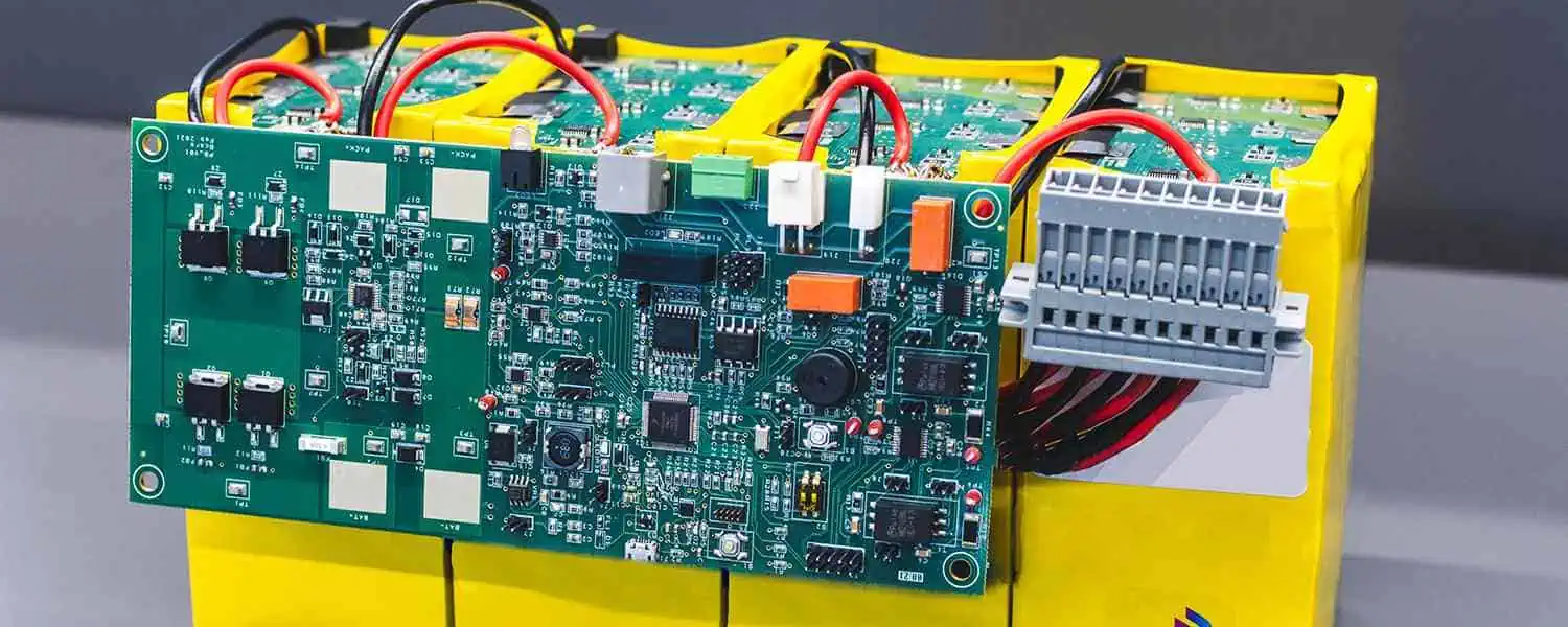
Introduction
Battery temperature sensors play an important role in battery management systems by providing temperature monitoring and protection. The measurement of cell, module, and pack temperatures allows the system to optimize charging conditions, prevent damage from overheating, and estimate battery capacity.
This article explores the impacts of temperature on battery performance and lifetime, the consequences of exceeding safe temperature limits, how and where temperature sensors are implemented, and alternatives when temperature sensing may not be required.
Effects of Temperature on Batteries
Battery cell chemistry determines optimal temperature ranges. In general, temperature extremes degrade batteries through the following effects:
High Temperatures
Accelerated ageing and shorter cycle lifetimes
Loss of active materials and internal structural changes
Increased self-discharge rates
Degradation of internal resistance and power capability
Thermal runaway risk in some lithium-ion types
Low Temperatures
Temporary loss of capacity and lower discharge rates
Increased internal resistance causes voltage drop
Reduced current and power discharge ability
Slower charging rates may be required
Risk of lithium plating in lithium-ion cells
Higher risk of metal corrosion in some chemistries
Keep batteries within a safe operating range improves performance, lifetime, and safety. Temperature monitoring provides feedback to manage these effects.
Without temperature monitoring and control, the following failure modes can occur when battery temperatures go out of safe limits:
High Temperature Effects
Pouch cell swelling leading to fire/explosion
Internal short circuits due to separator damage
Venting of electrolytes
Thermal runaway causing cascading cell failures
Low Temperature Impacts
Permanent capacity loss or premature failure
Internal battery damage from lithium plating
Voltage clipping and inability to deliver rated power
These potential risks demonstrate the need for temperature sensing as part of a battery management system.
Implementing Battery Temperature Sensors
To monitor temperature, sensor placement is important:
Cell Surface Mounting
Attaching sensors directly to cell surfaces provides most accurate measurements but increases pack complexity. Higher quantity of sensors required. Useful for validating cell models.
Module/Pack Mounting
Sensor mounted externally on module or pack enclosure is simpler. Provides general temperature for control but may not detect localized hot spots.
Within Pack
Sensors inserted internally between cells provide intermediate monitoring without direct cell contact. Compromise between complexity and localized readings.
Air Intake/Outflow
Measuring inlet cooling air and outlet heat exhaust temperatures provides indirect pack temperature estimates for basic control. Simplest approach.
Thermal Imaging
Infrared cameras used periodically provide non-contact temperature map of pack to identify hotspots not apparent from discrete sensors.
In most cases, a combination of pack surface sensors and selective internal placement provides sufficient temperature monitoring for control and protection.
Temperature Sensor Selection
A variety of sensor options exist for battery temperature monitoring:
Thermistors – Inexpensive, accurate. Linear and nonlinear types available.
RTDs – Very linear over wide temperature range. Accurate and precise but higher cost.
Compensation – Correct for errors like thermal junction effects in thermocouples.
Calibration – Normalize each sensor output at defined temperatures to maximize absolute accuracy.
Careful circuit design ensures the temperature sensor subsystem provides the battery management system with precision temperature data across the operating range.
Alternatives to Temperature Sensors
While temperature sensors are generally recommended, some alternatives exist for low cost or simpler battery packs:
Model Estimation
Use a thermal model of the battery to estimate temperature based on charge/discharge current, voltage response, and ambient temperature. Lower cost but less accurate.
Current Limiting
Conservatively derate maximum current to prevent heating rather than directly sensing temperature rise. Simple but reduces available capacity.
Periodic IR Scanning
Use a handheld thermal camera to periodically scan pack and check for hot spots instead of continuous monitoring. Only detects issues as they arise.
Exterior Thermal Feedback
Rely on skin temperature sensation, temperature labels, or surface mounted thermochromics to indicate unsafe externals temperatures manually. Provides warning but no control.
While workable for very basic systems, the lack of reliable temperature feedback with these alternatives prevents optimization and reduces safety margins compared to proper thermal sensing and control.
Advanced Temperature Monitoring
More advanced battery systems maximize safety and performance using improved thermal monitoring:
Multiple internal distributed sensors provide temperature maps to the BMS. Detects local hotspots.
Fiber optic distributed sensing embeds thousands of measuring points within modules to improve resolution.
Thermal runaway detection monitors rate of temperature increase as an early warning.
Cell surface insulators with embedded thermistors improve response time and accuracy.
Actively cooled and heated packs maintain uniform stable temperature regardless of conditions.
With sufficient temperature data, battery thermal models can be further refined to simulate thermal behaviors for different use cases and optimize thermal management strategies.
Thermal Management Integration
Incorporating temperature data into thermal management enables:
Reducing charge rate when temperature nears limit to avoid overheating rather than simple fixed current charging.
Proactively cooling the pack when approaching upper limits well before reaching critical temperatures.
Preventing operation in extremely cold environments by temperature dependent output derating or pack heating.
Optimizing cooling system controls based on inlet air and internal temperatures.
Estimating impedances and available capacity based on temperature.
Triggering safe shutdown and isolation when dangerous temperatures are detected.
Integrating temperature monitoring as part of the overall thermal management and battery management systems is key to maintaining safe, efficient, and optimal battery operation.
Summary
Battery temperature heavily impacts performance, lifetime, and safety parameters. Exceeding limits degrades batteries.
Direct temperature monitoring allows optimizing operation as well as preventing failures from overheating or freezing.
Sensor selection, placement, and circuit design ensure robust and noise-free measurements for the battery management system.
Alternatives exist for simple batteries but lack protections of active sensing and control. Advanced techniques provide greater resolution.
Temperature feedback coupled with thermal management strategies maximizes battery efficiency, utilization, and safety.
FAQ
How many temperature sensors are needed in battery pack?
Depends on pack size but a minimum of 3-5 sensors placed at end/middle of pack helps detect basic thermal gradients for control and protection. Larger packs may use 10 or more sensors distributed throughout the modules.
What temperature range do Li-Ion batteries operate in?
Charge: 0°C to 45°C, Discharge: -20°C to 60°C. Wider operating range possible with thermal controls. Lower and upper cutoff limits are used for protection.
What communications bus is used for battery temperature sensors?
A controller area network bus (CAN Bus) is typical for connecting multiple sensors over a common serial data bus. Other options include SPI, ISO-BUS, and I2C. Wireless sensors are also an emerging option.
How often should battery temperature be monitored?
Continuous monitoring provides best results for optimizing charging and prevent over-temperature conditions. For simple packs, occasional sampling may suffice but lacks robust protections.
Why are multiple temperature sensors needed in large battery packs?
A single external measurement cannot detect internal hot spots. Distributed sensors allow finding cells with higher localized heating to properly control charge rates and cooling across large packs.
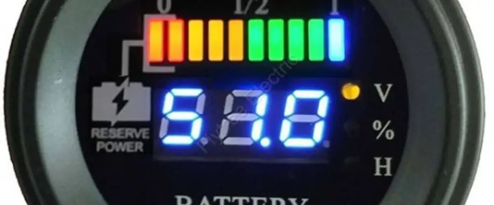
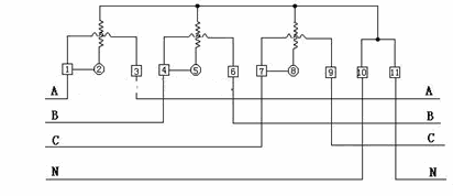
Three-phase watt-hour meter is used to measure the power output (or load consumption) of three-phase ac circuit. Its working principle is exactly the same as that of single-phase watt-hour meter, except that it adopts the way of multiple driving parts and aluminum plates fixed on the rotating shaft in structure to realize the measurement of three-phase electric energy.
Three-phase three-circuit active watt-hour meter uses two sets of driving parts to act on two aluminum plates (or one aluminum plate) mounted on the same shaft, and the principle is exactly the same as that of single-phase watt-hour meter.
The three-phase watt-hour meter fully meets the technical requirements of single-phase 1 or 2-stage in DL/ T645 -1997 and GB/ T17215-1998.With good reliability, small size, light weight, beautiful appearance, advanced technology, 35mm DIN standard installation and other characteristics;And has a good anti – electromagnetic interference, low self – consumption power saving, high precision, high overload, high stability, anti – electric leakage,Long Service life.
Introduction
A watt-hour meter, also known as a kilowatt-hour meter, is an electrical meter that measures the total energy consumed by a residence, business, or an electrical load in kilowatt-hours. It allows power utilities to determine power consumption over a period of time for billing purposes and customers to monitor their electrical energy usage.
This article provides an overview of watt-hour meter operating principles, design types including electromechanical and electronic meters, key components, installation considerations, calibration and accuracy, and trends in smart metering technology.
What is a Watt-Hour and Why Measure It?
A watt-hour is a unit of electrical energy equivalent to a power consumption of one watt sustained for one hour. For example, a 100 watt light bulb powered for 10 hours would consume 1000 watt-hours of energy (100 x 10 = 1000 watt-hr).
By measuring watt-hours, the total work performed or energy consumed by an electrical load can be determined. The utility company uses this information to properly bill customers based on energy use rather than simple power (watts) draw. Customers can also monitor watt-hour usage over time to identify high consumption loads or changes in energy usage profiles.
Some key reasons to measure watt-hours:
Allows fair utility billing based on total energy consumed rather than peak power demand
Enables analyzing usage patterns over days, weeks, months to minimize waste
Identifies high consumption equipment for possible efficiency improvements
Verifies conservation efforts are achieving savings
Provides data to size backup power systems and generators
Operating Principle
Watt-hour meters operate on the principle of counting revolutions of an aluminum disc mounted on a shaft. The disc rotates at a speed proportional to the power flowing through the meter. Counting the revolutions over time therefore provides a measurement of the energy consumed.
The aluminum disc spins between two electromagnets. One creates a magnetic flux proportional to the voltage applied. The other uses current flowing through the meter to generate a magnetic field. The interaction of these two perpendicular magnetic fields produces a torque that rotates the disc at a speed proportional to power (volt-amps).
Gears connect the disc to dials which record the cumulative energy consumption. This method allows the meter to register the total watt-hours used over months or years.
Electromechanical Watt-Hour Meter Operation (Image Credit: BidyutJyoti/Wikimedia)
Types of Watt Hour Meters
There are two primary types of watthour meters in use:
Electromechanical
The traditional electromechanical induction meter uses the rotating aluminum disc as described above. Gears drive mechanical dials to display the watt-hours used.
They provide reliable measurement but are bulky and require manual reading. Electromechanical meters are still in use but being phased out in favor of electronic meters.
Electronic
Newer electronic watt-hour meters replace the physical disc and gears with electronic sensing and measurement of voltage and current. This allows features like:
LCD/LED numerical display of usage rather than dials
Ability to network multiple meters with remote reading
Programmable time-based tariff schedules
Instantaneous power usage readout
Two-way communication for meter configuration
Load control capabilities
Electronic meters are cheaper to produce and enable automated meter reading and advanced smart grid functionality.
Watt Hour Meter Components
The key components found in a watt-hour meter are:
Voltage coils – Apply magnetic flux to aluminum disc proportional to line voltage
Current coils – Generate magnetic field proportional to current flow through meter
Rotating disc assembly – Spins at speed proportional to power consumption
Damping magnet – Stabilizes disc rotation speed to prevent overspinning
Gears – Provide mechanical coupling to dials/display
Dials or display – Cumulatively show watt-hours consumed
Test block – Allows magnetic calibration and accuracy testing
Registers – Record cumulative energy usage over time
Major Components in an Electromechanical Watt-Hour Meter (Image Credit: BidyutJyoti/Wikimedia)
Watt Hour Meter Installation
Proper installation of watt-hour meters is important for accurate measurement:
Mount securely on non-flammable surface away from easily combustible materials
Locate outdoors in protective housing if required by standards
Position the meter so display is easily visible without obstructions
Verify meter socket wiring matches meter terminal design and rated voltages
Use weatherproof conduit fittings aligned properly with enclosure
Leave sufficient wire slack to prevent stresses on connections
Seal openings and knockouts according to local electrical code
Check disc rotation direction and multiplier connections
Verify calibration and seals following installation
Careful mechanical and electrical installation protects the meter and ensures correct energy accounting right from the start.
Calibration and Accuracy
Watt-hour meters are factory calibrated to standards specifying allowed tolerances on errors. Typical accuracy metrics:
Full load – 0.5% to 1% error at nominal current rating
Light load – 1% to 2.5% error at 10% of nominal current
Power factor – 1% to 3% error over 0.5 lagging to 0.8 leading
Various factors impact accuracy:
Magnet strength weakening over time
Bearing wear allowing disc wobble
Dust buildup on critical components
Voltage imbalance between phases
Field calibration and testing procedures help maintain accuracy:
Calibration check at full, light, and zero load
Verify disc rotation speed using timing marks
Current reversal test detects loose or tilted discs
Optional calibration magnets can correct minor errors
Adhering to recommended recalibration intervals ensures minimal watt-hour reading errors.
Trends in Smart Metering
Traditional electromechanical watt-hour meters are increasingly being replaced by sophisticated electronic smart meters that provide additional capabilities:
Two-way digital communication for automatic meter readings
Real-time power usage monitoring
Load limiting and load shedding abilities
Remote reconfiguration and setting of tariff schedules
Power quality metrics like voltage, frequencies, power factor
Tamper and theft detection alerts
Outage reporting and power restoration logging
When networked together into the advanced metering infrastructure (AMI), smart meters allow:
Automated billing and reduction in overhead
Remote insight into demand and grid health
New time-based electricity pricing models
Ability to collect and analyze energy usage data
The transition to smart meters and AMI is a crucial step in modernizing power grids and enabling greater efficiency and reliability through information availability.
Summary
Watt-hour meters measure the total electrical energy used by a load, residence, or facility. This enables utility billing based on consumption.
Traditional electromechanical types used eddy currents and an aluminum disc but are being replaced by electronic meters.
Accurate voltage and current sensing allows determining power usage. Disc rotation per time indicates energy usage.
Careful mechanical and electrical installation is needed for reliable operation. Meters must be periodically calibrated.
Evolution to smart meters provides automation, telemetry, grid analytics, and usage visibility through networked communication.
FAQ
How does a watt-hour meter work electrically?
It works by sensing the voltage and current to derive real power. Two coils generate magnetic fields proportional to the voltage and current. Their interaction causes a disc to rotate at a speed proportional to power. Counting revolutions over time provides energy usage.
What was the main limitation of electromechanical watt-hour meters?
The primary limitation was the need to manually read and record the dial indications to determine electrical energy usage. This was labor intensive and prevented real-time telemetry of consumption data. Modern electronic meters overcome this through digital outputs and networking.
What quantities can smart meters measure beyond watt-hours?
Smart meters contain additional electronics to measure parameters like power factor, voltage, current, frequency, waveform quality, instantaneous usage, and outage information. This provides greater grid and usage insight.
How frequently are utility watt-hour meters calibrated?
Electromechanical meters are typically recalibrated every 5-10 years. Electronic smart meters are solid-state with no moving parts and generally do not need recalibration for 15-20 years assuming acceptable power conditions.
How does meter tampering impact watt-hour accuracy?
Any unauthorized physical alteration like forcing discs to under-record usage, applying external magnets, or electrical tampering will greatly reduce meter accuracy. Smart meters often include tamper detection capabilities to detect and report such activities.