PCB manufacturers are familiar with a lot of materials. For a PCB to function well, several materials are used. However, some materials are specifically designed to meet some certain demands. Arlon 47N isn’t just a regular PCB material. This material is specially designed for heat sink bonding applications. Therefore, we will look further into this material and what it offers.
What is Arlon 47N PCB Material?
Arlon 47N PCB material is a low-flow epoxy prepreg designed for fixing heat sinks to multilayer boards. Also, this material is ideal for bonding multilayer epoxy. It features a minimal lamination temperature that shields components mounted on circuit boards. Arlon 47N is an improved epoxy low flow prepreg system with excellent properties.
This material features discrete fiberglass styles and flow ranges for enhanced process flexibility. Arlon 47N features excellent mechanical, thermal, and electrical properties. All of these properties meet the PCB industry standards. In addition, Arlon 47N PCB material is a cost effective option for high volume commercial applications.
The glass transition temperature of Arlon 47N is 135 degrees Celsius at TMA and DSC. This is a very low Tg value. This means that this material can’t function well in a high thermal environment. Arlon 47N can transform from a solid state to a rubber-like state when it is at 135 degrees Celsius.
High decomposition temperature
The decomposition temperature of this material is 305 degrees Celsius. This means that this material won’t decompose easily. Also, it can only decompose chemically when it is at 305 degrees Celsius. However, the decomposition temperature at 5% weight loss is 315 degrees Celsius.
Very low dissipation factor
The dissipation factor of Arlon 47N PCB material is very low. Also, it features a dissipation factor of 0.02 at 1MHz. Therefore, this material can hardly absorb or discharge heat when exposed to varying temperatures. Also, it is a good insulator system.
Low CTE
The coefficient of thermal expansion is 16 ppmo/C at both X and Y axis. However, the Z-axis CTE is 85 ppmo/C. Therefore, this material can withstand varying degrees of temperature without expanding easily.
High peel strength
Arlon 47N PCB material features very high peel strength. The peel strength is 9.0 (1.6) Ib/in (N/mm) at increased temperatures and after thermal stress. Also, this value is the same after process solutions. This property helps 47N offer great bonding to multilayer boards.
Great surface resistivity
The surface resistivity of Arlon 47N is 8.8 x 10⁶ at C96/35/90. Also, surface resistivity of this material is 1.5 x 10⁶ at E24/125.
Low water absorption
The water absorption rate of 47N is 0.1%. Therefore, this material is ideal for use in PCBs used in humid environments.
Use the standard practices in the industry to process inner layers. The inner layers should be baked for 60 minutes between 107 degrees Celsius and 121 degrees Celsius. Also, this vacuum desiccates the prepreg system for about 12 hours before lamination.
Below are the lamination and drilling processes:
Pre-vacuum within 30-45 minutes
Regulate the rise of heat to about 12oF per minute.
The cure temperature of the product should be 171 degrees Celsius.
Cure time at temperature should be 1 hour.
Use alkaline permanganate to desmear. Also, you can use plasma desmear. Plasma is ideal for achieving positive etchback.
Arlon 47N PCB material is compatible with conventional plating processes
You can make use of standard profiling parameters. However, we don’t recommend chip breaker style routers.
Also, you should bake for 1 to 2 hours at 121 degrees Celsius before HASL or solder reflow.
Impacts of Low Glass Transition Temperature on Arlon 47N
The low glass transition temperature (Tg) is an important property in PCB materials. This property measures the temperature at which Arlon 47N transforms to a rubber-like state. Also, this value determines the mechanical stability of this material.
Arlon 47N offers a low Tg value. Therefore, this material offers a smaller expansion than materials with high Tg values. The operating temperature of Arlon 47N must not exceed 135 degrees Celsius. Arlon 47N will maintain its solid structure if it isn’t exposed to temperatures beyond its limit. Also, the glass transition temperature of Arlon 47N is low. However, a material with high Tg value is ideal for PCBs subjected to hot environments. Therefore, Arlon 47N can only function well below 135 degrees Celsius.
There are several benefits offered by Arlon 47N. This material offers exceptional benefits. Therefore, these benefits include:
Industry approval
Arlon 47N meets the requirements and specifications of most industry standards. Also, the electrical and mechanical properties meet the specifications of IPC-4101/21. In addition, Arlon 47N complies with RoHS/ WEEE standards. Therefore, this PCB material is ideal for PCB fabrication.
Great bond strength
Arlon 47N has improved bond strength to copper. Therefore, it provides great performance in heat sink bonding. Also, the cure temperature of this material is as low as 150 degrees Celsius.
Optimal process flexibility
This material features great process flexibility. This is because of its discrete fiberglass styles and flow ranges. Also, the reduced lamination temperature shields components installed on the PCB.
Cost effective
Arlon 47N is a cost-effective option for PCB fabrication. Therefore, it is suitable for high volume commercial applications.
Great performance
Arlon 47N PCB material offers properties that contribute to its great performance.
Lead-free process compatibility
Arlon 47N has no lead components. In addition, it is compatible with lead-free processing. Therefore, it is an ideal polyimide prepreg system for circuit boards.
Arlon 47N PCB material is primarily designed for bonding multilayer epoxy. This material is useful in:
Bonding multilayer epoxy rigid-flex
Dielectric insulators
Attaching heat sinks to polyimide multilayer boards.
Conclusion
Arlon 47N is a PCB material with exceptional properties. Also, this material was specially formulated to bond multilayer epoxy rigid-flex. In this article, we have discussed the impact of this material on PCB fabrication.
The use of PCB materials for printed circuit boards, as well as other applications is important. This is one reason why it is necessary to make use of a high quality one to ensure that you get the very best delivery.
In this article, we will be talking about the Arlon 45N PCB Material. This is the multifunctional epoxy prepreg and laminate. What this simply means is that it can serve many functions. We will discuss what this material is, its features, application, properties, and recommended process conditions.
If this is of great interest to you, please continue reading. We have a lot in stock for you.
The Arlon 45N PCB Material is known to be tough, and has a high temperature of glass transition with a value of 175 degrees Celsius by DSC. It is a prepreg system and multifunctional epoxy laminate, which is useful in different higher layer count multilayer boards. Making use of the conventional conditions for FR-4, you can process them.
They are relevant in applications such as mother boards and black planes, BGA packaging, multilayer boards of high layer count, and automotive applications. Let’s go into details of the features of this multifunctional material.
What are the Features of the Arlon 45N PCB Material?
The features of the Arlon 45N PCB Material is as follows
Great for a large number of lead-free applications. This PCB material serves different lead-free applications. This means that these applications don’t use lead because of their harmful nature.
Its flammability rating is UL-94 V0. This is the standard the UL has set to help in testing a material’s flammability which means that on any vertical specimen, burning stops in ten seconds.
It has a high glass transition temperature at 175 degrees Celsius. This means that this pcb material has a strong ability to develop glassy-state properties like rigidity, stiffness, and brittleness upon cooling.
Meets the IPC4101/26 specification and description
Also, it is RoHS/WEEE compliant. This means that it has been regulated for any hazardous substance utilized in manufacturing electronic and electrical equipment. This means that this pcb material has passed the RoHS/WEEE compliance.
Resists cracking of the inner layer copper and barrel cracking when fabrication is on
Its peel strength with respect to copper is 8 N/mm after thermal stress. Then at elevated temperatures, it stands at 8 N/mm, while after process solutions, the value is 8 N/mm
Recommended Process Conditions of the Arlon 45N PCB Material
The recommended process conditions of the Arlon 45N PCB material is as follows.
For the Arlon 45N, process the inner layer through strip, etch, and develop making use of the standard practices of the industry.
Furthermore, on the inner layers, make use of brown oxide. Also, adjust the dwell time present in the oxide bath. This makes sure that there is uniform coating.
In addition, bake the inner layers in the rack for an hour at a temperature between 225 degrees Fahrenheit and 250 degrees Fahrenheit. This should be done before lay-up. Also, the prepreg should be vacuum desiccated for about 8 to 12 hours before you laminate.
For the lamination cycle, pre-vacuum it. This should be done for thirty minutes. Also, control the rise in heat to 8 – 12 degrees Fahrenheit every minute between 210 to 300 degrees Fahrenheit.
In addition, the product temperature during the start of cure should be 360 degrees Fahrenheit. Also, the cure time should be 90 minutes. Lastly, cooling down should be done under a maximum pressure of 12 degrees Fahrenheit.
Conclusion
The Arlon 45N PCB Material is known to be tough, and has a high temperature of glass transition with a value of 175 degrees Celsius. Also, it is a prepreg system and multifunctional epoxy laminate, which is useful in different higher layer count multilayer boards. Also, we have discussed its properties, features, applications and other necessary information. If you have any more questions, please feel free to contact us. Furthermore, RayMing PCB is a professional manufacturer of the Arlon 45N PCB Material. Contact us today for the very best!
The Shengyi S1000-2 PCB material offers optimal performance because of its resistance to high heat. This laminate is uniquely designed with little water absorption which is one of the distinct features it possesses. Also, the Shengyi S1000-2 comes with an FR-4 laminate component which is lead free.
Before writing this article, we ensured that we researched every component of the Shengyi S1000-2 PCB material. We found out that this laminate has some amazing features which set it apart from any other laminates. Therefore in this article, you shall find out everything you need to know about the Shengyi S1000-2 PCB material.
First, you need to know that this is a laminate which helps circuit boards have excellent features. Plus, the Shengyi S1000-2 has exceptional anti-CAF conduct. Besides this, it has exceptional thermal resistance and has first-rate through hole accuracy.
The Shengyi S1000-2 is an excellent class of laminate that designers and engineers use to connect various layers of the multilayer circuit board. Meanwhile, this Shengyi S1000-2 helps the connection become firm. Thus, the bond becomes lasting and the PCB board is durable. This is because the laminate secures the layers, protecting it from extreme heat and any humidity effect.
The Shengyi S1000-2 is an FR-4 circuit board component which has some low CTE. Thus, it also has High-Tg. It comes with PCB processability and exceptional adhesion components.
What are The Features of The Shengyi S1000-2?
This laminate has some features that enable it to protect the PCB layers and also makes it avoid any form of moisture effects.
It is important you study the Shengyi S1000-2 PCB material carefully so as to understand its features. When you understand its features perfectly, then you can know the class of laminate this Shengyi S1000-2 is.
UV Resistance and High-Tg
This is one of the important features of the Shengyi S1000-2 PCB material. It is resistant to ultraviolet radiation and as such can hurdle the effects it may have on the PCB layers.
Plus, the Shengyi S1000-2 has a tall glass conversion temperature. Hence, this temperature has the possibility of getting as high as 170 degrees. This is a laminate that has the possibility to always retain its resistance to UV light so that the PCB board wouldn’t be exposed directly to radiation.
The Shengyi S1000-2 PCB material has a very compatible Lead free component which includes the FR-4 circuit elements. As a result of this, it is very safe to use this type of laminate on PCB layers.
Therefore, the Shengyi S1000-2 helps protect the circuit board against environmental pollution as well as any harmful substances. Due to that, the Shengyi S1000-2 always uses lead free compatible FR-4 laminate components.
Exceptional Through Hole Accuracy
This laminate allows material mounting. Plus, one can be certain that drilling into the holes is plausible using the Shengyi S1000-2 PCB material.
Engineers and designers can drill various kinds of holes ranging from small, medium to large sizes into this laminate. Therefore, it becomes so compatible.
High Heat Resistance
One thing is, we cannot overemphasize this feature. When you think of laminate that has high resistance to heat, the Shengyi S1000-2 PCB material is one to use. Interestingly, one can apply this laminate in any temperature, especially high temperature. Owing to its great heat resistance, no negative effect occurs on the PCB layers. It is stable to retain its high temperature resistance at all times.
Low Water Absorption
This laminate is unique because it has low water absorption. This implies that there is a low rate for water to pass through it. Therefore, it always prevents water from entering it at all cost. Concurrently, no matter the moisture, this laminate can withstand water absorption.
Interestingly, one can make use of the Shengyi S1000-2 PCB material in various applications. Therefore, it serves multiple functions.
Automobiles
One can apply this laminate on automobiles. Regardless, you can move it anywhere. It enhances your automobiles performance. As a result, it protects the automobiles from any hazardous damage.
Computers
You can apply this laminate for effective communication in computers. It is mostly available in phones and computers.
Now, there are waterproof smartphones that are resistant to water. This laminate makes it possible.
Router Equipment
There is the application of the Shengyi S1000-2 on routers. Thus, it makes it easier for internet connections. Interestingly, it also has dust resistance apart from resistance to water and heat. Therefore, one can use this laminate for routers.
Advantages of Using The Shengyi S1000-2 PCB Material
There are numerous advantages of using this kind of laminate for your circuit boards or automobiles.
Durability
When it comes to long-lasting laminate, the Shengyi S1000-2 has potential to be durable. It is resistant to harsh environmental pollution. At the same time, it can withstand humidity or heat conditions.
Quicker Processing Modes
It has speed when it comes to processing. The processing modes are quicker than any other type of laminates. Your PCB board can operate faster than you can imagine with the Shengyi S1000-2.
This is one advantage with this laminate. Earlier we discussed that you can apply the Shengyi S1000-2 PCB material on automobiles, phones, and computers. Thereby, it performs multiple functions. It has a tendency to perform effectively on various applications.
Easy to Design
The Shengyi S1000-2 PCB material is very easy to design. Wherefore, anyone interested in designing this laminate can find it easy and interesting to do. Also, it allows you to be creative and innovative with your designs.
Conclusion
The features of the Shengyi S1000-2 PCB material are numerous. It is a kind of laminate that designers enjoy using for their circuit board.
Also, this is a class of laminate that is weather resistant. This implies that it is applicable for use under sunshine or rain. Plus, it is highly durable and resistant to high temperatures. You can test its flammability, volume resistivity, and dielectric components. These are some of the properties of this laminate you can always test.
There are different reliable materials for printed circuit boards. The materials or laminates from Isola are known for their high performance and usually feature in resin formulations. These laminates’ designs are top-quality. Furthermore, with their great features, it will surely meet the needs of any demanding requirements for complex printed circuit boards.
In this article, we will be answering whatever questions you have on your mind regarding the Isola FR408hr PCB material. If you desire learning about the options necessary for treatment, the quality, features, benefits of this PCB material, we have everything covered in here.
The Isola FR408hr PCB material has to do with the high-performance prepreg and FR-4 laminate system. Furthermore, this PCB material is great for multilayer printed circuit boards where there’s a need for thermal performance and maximum reliability.
Furthermore, this PCB material integrates the copyrighted multifunctional high performance epoxy resin system of Isola, which has been strengthened with the use of E-glass fabric.
Also these features along with its great moisture resistance, helps in the creation of a product which closes the void from a thermal and electrical aspect.
Features of the Isola FR408hr PCB Material
Below are the main characteristics and features of the Isola FR408hr PCB material
Prepreg appears like a roll or panel
The Isola FR408hr PCB material has a temperature of glass transition of 230 degrees Celsius
Important Mechanical Properties of the Isola FR408hr PCB Material to Consider
Below are some of the main mechanical features of the Isola FR408hr PCB material, which you must consider.
Peel Strength
This is the measure of the bond strength between the Isola FR408hr PCB material and its copper conductor. 180 degrees should be the separation angle. Furthermore, the test of the peel strength has to be finalized under these conditions.
After the thermal stress where the Isola FR408hr PCB material is floated on solder for about 10 seconds at a temperature of 288 degrees Celsius.
Also, at temperatures that are elevated where the Isola FR408hr PCB material is exposed to air or hot fluid at a temperature of 125 degrees.
The last condition is after the exposure of the process chemicals where the product is subjected to some procedures in a chemical or thermal process.
Note that after the thermal stress, the Isola FR408hr PCB material has a peel strength of 5.5 lb/inch. Also, after the process solutions, it has a peel strength of 5.1 lb/inch.
Delamination Time
This signifies the time the Isola FR408hr PCB material will resist delamination. Delamination has to do with the resin separation from laminate, fiberglass, or foil, at a given temperature. At 260 degrees temperature, the delamination time for the Isola FR408hr PCB material is I hour. At a temperature of 288 degrees, the time is 30 minutes.
Young Modulus
This is also the tensile modulus and it also determines the strength of the Isola FR408hr PCB material. However, this also evaluates the ratio of the strain over the stress in any direction.
This mechanical property has a measurement unit along the length direction of 3695 ksi and along the cross direction, it has a value of 3315 ksi.
Flexural Strength
This property determines the Isola FR408hr PCB material’s capacity to fight against or endure any mechanical stress and stay without breaking.
This test involves the support of the edges of the Isola material, coupled with the applying of the load at the middle. In the length direction, the Isola FR408hr PCB material has a flexural strength of 72.5 ksi. Also, at the cross direction, the Isola FR408hr PCB material has a flexural strength of 58.0 ksi.
The system of the Isola FR408HR PCB material has great UV blocking, as well as laser fluorescing. With this, you are sure to enjoy maximum compatibility with AOI systems, solder mask imaging (photo-imageable), and systems of optical positioning.
As a result of this, this ensures throughput and high accuracy when constructing and assembling the Isola FR408HR PCB.
Lower Loss and Enhanced Expansion of the Z-axis
The Isola FR408HR PCB material offers an advancement of 30% in the expansion of the Z-direction. However, this delivers a lower loss as well. This means an additional 25% when it comes to electrical bandwidth compared to other competing products.
Other benefits of the Isola FR408HR PCB material include:
There are many benefits of using Arlon 85NT PCB material for your applications as well as circuit boards. Apart from useful areas of applications, this laminate material is one of the widely used PCB materials by designers and engineers. This pure polyimide laminate material is produced from aramid substrate which is known to be non-woven.
In this article, you shall find out interesting information about Arlon 85NT PCB material and what this prepreg system works for. Also, it is highly durable and doesn’t absorb water like some other laminates and prepreg systems.
What Kinds of Resistance Does Arlon 85NT PCB Material Have?
Each prepreg system and laminate material has different kinds of resistance. The ability to resist certain degrees of temperature or extra heat solely depends on the properties of such laminate. Also, the materials used in fabricating such prepreg systems determine if such PCB material can withstand unfriendly or toxic environmental factors. However, let us consider some Arlon 85NT resistance traits.
This is one of the kinds of resistance this prepreg system has. This feature makes Arlon 85NT have potential to resist flow of heat both on its internal and external surfaces. This laminate material can indicate thermal resistance in all its applications. Therefore, this laminate works in high temperatures. It has exceptional thermal reliability which distinguishes it from other prepreg systems.
Water Resistance
This is very important for all laminates and prepreg systems. Although the level at which laminates can absorb water is considerably different. This laminate is waterproof and has a low rate of water absorption.
Thereby, it has the capacity to hold water. It serves as a barrier to moisture condensation or doesn’t allow the flow of water through its components. Hence, this laminate is durable and works in diverse applications and different atmospheres.
CAF Resistance
The Arlon 85NT PCB material can withstand the procedures for electrochemical corrosion or migration. Interestingly, this aids how long lasting this laminate material can be. This prepreg system has the ability to retain its high performance because of its CAF resistance.
UV Resistance
This prepreg system can resist any ultraviolet radiation which often affects the performance of many PCB materials. Since it can block any ultraviolet radiation, it makes it become durable. Therefore, heat, high temperature or light radiation can’t affect this laminate material because of its resistance rate.
The Advantages of Using The Arlon 85NT PCB Material
There are many benefits that come with using this type of prepreg system. It works effectively for most applications because of its potential to resist some dangerous environmental conditions.
High Rate of Resistance
Earlier we listed the different kinds of resistance levels this laminate material has. One benefit with using Arlon 85NT is that its resistance rate is high such that no harmful chemicals or UV light, high degrees of temperature can affect it. This is one thing to always check out for in PCB materials.
Simple Processing Modes
When it comes to the processing modes of Arlon 85NT, it is very simple. This kind of laminate doesn’t require extra procedures for processing it. The processing modes are quicker and simpler in comparison to other PCB materials. It has faster speed when in operation in many applications or multilayer circuit boards.
Durability
This is one advantage of using this prepreg system. When it comes to high durability, this PCB material is one that gives you value for your money. This is because engineers and designers always ensure this material is compatible with lead free assembly. Thus, it can be potent for years connecting multilayers in the circuit boards.
Multiple Performance
When we talk about versatility, this is the laminate material to opt for. This is because it serves multiple purposes for different applications. That is why it is easier to use Arlon 85NT for various applications. It is not a rigid kind of prepreg system that works only on one type of application.
Thermal Stability
We shouldn’t forget that the ability to retain stability under high temperature is one unique feature of this laminate material. With increasing temperature, this prepreg system can still work without any hindrance.
It is paramount to always check out for the mechanical properties of this laminate material. This prepreg system with exceptional dimensional stability has the following mechanical components.
When you apply force on this material, these mechanical properties are liable to change afterwards. Therefore, it is paramount to consider these mechanical properties very well.
Peel Strength
This is one of the mechanical properties of Arlon 85NT that designers look out for. This is because it can enhance bonding of this laminate on various kinds of surfaces. However, with too much force, the peel strength may become affected.
Elasticity Modulus
You should consider the potential of this prepreg system to withstand any deformation resulting from heat application. When you apply heat on laminates, it has the possibility of changing form. This implies that it requires accurate measurement for the elasticity modulus of Arlon 85NT.
Poisson Rate
You need to consider the ratio of modification involving the width for each unit of this type of laminate material. The ratio of modification shows how change occurs per width of Arlon 85NT. Therefore, it alters modification in length of each unit length of the prepreg system.
Note that one can use this prepreg system in various areas. There is no restriction to the diverse fields a designer can use. Therefore, in optical communication services, medical, defense, legal, and automobiles, one can use this laminate material without any hindrance. It works for applications irrespective of the degrees of temperature of such an environment.
Conclusion
Arlon 85NT PCB material is durable and is weather resistant. One of the key resistance to check out for is the thermal resistance. This is because it indicates how it works in varying degrees of temperature. The mechanical properties of this laminate material are important. You should check out for its peel strength among other mechanical properties. No doubt, this prepreg system works in various applications and gives value for your money.
Printed circuit boards (PCBs) form the backbone of electronics products. Their fabrication and assembly provides employment to hundreds of thousands globally. PCB manufacturing involves creating the bare printed circuit boards. PCB assembly populates the boards with components to produce functional printed circuit assemblies (PCAs). While interconnected, PCB manufacturing and circuit board assembly involve distinct processes and require different skills.
This article examines and compares various roles and responsibilities in PCB fabrication jobs versus circuit board assembly jobs. It provides insights into the work environment, technical skills, qualifications, training, and career growth opportunities associated with each area.
Overview of PCB Manufacturing Jobs
PCB fabrication transforms base materials like laminates and copper foils into complex, multi-layer circuit boards ready for component mounting. Manufacturers employ operators, technicians and engineers across these key departments:
PCB Processing
Involves equipment operation for processes like:
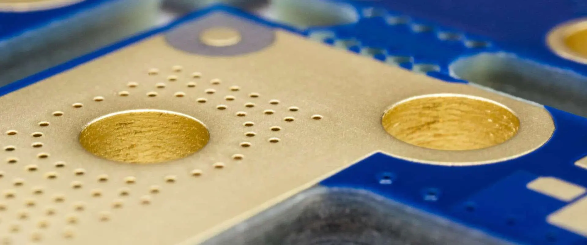
Drilling – Creates holes for vias and component leads
Plating – Deposits copper in drilled holes and on surfaces
Coating – Applies photoresist for imaging conductors
Assist engineers with process troubleshooting and improvement
Support changeovers between PCB designs and orders
Inspection Technicians
Perform visual inspection of PCBs at each process step
Use optical systems to measure conductor widths, spacing and hole sizes
Execute electrical testing like continuity checks and isolation resistance
Document inspection results on travelers and logs
Generate discrepancy reports for failed boards
Prepare certification packages with inspection data
Quality Engineers
Develop inspection plans and sampling criteria
Create procedures for measurements, testing and reporting
Conduct failure analysis on defective boards
Identify root causes and corrective actions
Monitor process performance and quality metrics
Lead continuous improvement initiatives
Maintenance Technicians
Execute preventive maintenance like cleaning and lubrication
Diagnose and troubleshoot equipment failures
Repair or replace defective components
Align and calibrate machines to specifications
Document all maintenance and repair activity
Support equipment installations and upgrades
Key Skills Needed for PCB Manufacturing Jobs
Essential skills for PCB manufacturing roles include:
Equipment Operation: Knowhow to correctly operate and control equipment like drilling machines, plating tanks, exposure units and solder mask screen printers.
Process Knowledge: Understand chemistry, parameters and procedures for processes like developing, etching, stripping and legend printing.
Inspection: Able to perform visual inspection and use tools like microscopes, calipers and electrical testers.
Testing: Skills in testing PCB characteristics like solderability, electrical properties and chemical concentrations.
Quality Systems: Know techniques like sampling, SPC, root cause analysis and corrective actions.
Math: Must apply math for calculations like solution concentrations, production yields and process capability ratios.
Technical Documentation: Can read and interpret specifications, procedures, drawings and datasheets.
Communication: Able to share information clearly between shifts, teams and departments.
Troubleshooting: Diagnose and debug issues with equipment, processes and materials.
Safety: Follow all chemical, electrical and machine safety procedures.
Education and Training for PCB Manufacturing Jobs
Test Electronic Components on a Circuit Board
Typical education and training pathways into PCB manufacturing include:
High school diploma or GED
Technical certification in electronics manufacturing
Associate degree in electronics engineering technology
On-the-job training on equipment and processes
IPC training for standards like IPC-A-600, IPC-A-610, IPC J-STD-001
OEM training on proprietary equipment and procedures
Certifications like CIT (certified IPC trainer) and CIS (certified IPC specialist)
Advanced roles like process engineering or quality engineering require bachelor’s or master’s degrees in engineering disciplines.
Continual skills upgrading through refresher training is essential due to evolving PCB technology.
Career Growth in PCB Manufacturing
Typical career growth paths in PCB fabrication include:
Operator > Lead Operator > Supervisor > Production Manager
Operators can progress to lead roles with coaching skills. Further advancement possible into production supervision and management.
Technician > Senior Technician > Engineer
Technicians can transition into senior tech roles with additional training on new processes and equipment. Some progress into process engineering positions.
Engineers can evolve from working on a process to leading entire new product introduction or manufacturing engineering. Management roles possible for senior engineers.
Manager > Director > VP Operations
Managers expand scope from one department to multiple departments or site leadership. Progression into executive roles like VP operations possible with experience.
Overview of Circuit Board Assembly Jobs
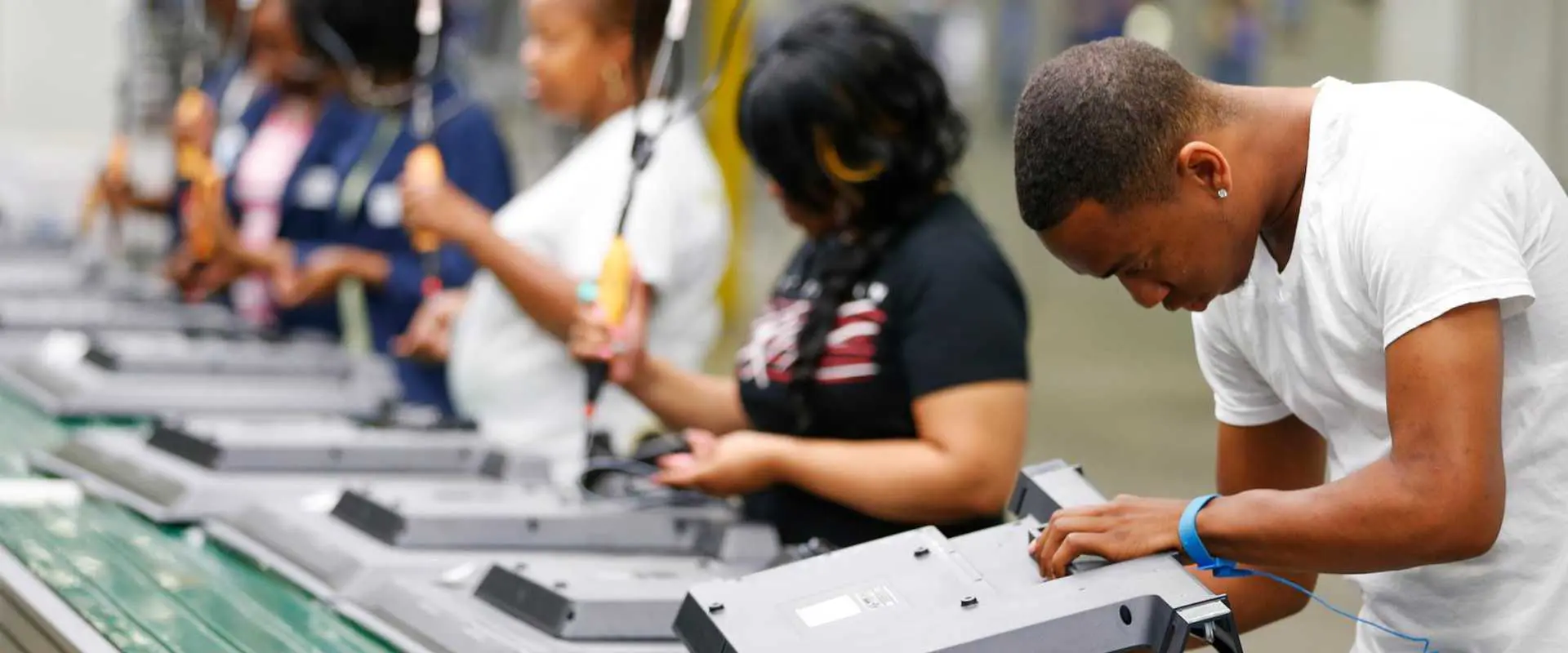
Printed circuit board assembly (PCBA) involves mounting and soldering electronic components onto PCBs using both automated and manual processes. Key departments are:
Cleanroom environment for many processes. Chemical usage.
Production floor environment. ESD control required.
Qualifications
High school diploma or IPC training certification. Associate degree preferred.
High school diploma. IPC training a plus. Associate degree helpful for test engineering roles.
Critical Skills
Operating fabrication equipment. Performing process steps like developing and stripping. Conducting inspection and testing.
Operating SMT and through-hole assembly equipment. Manual soldering techniques. Conducting inspections and testing like ICT and AXI.
Training
On-the-job training on specific equipment. IPC programs for standards knowledge.
Training on assembly procedures. IPC-A-610 and J-STD-001 certification. ESD control.
Career Growth
Progression from operators to technicians and engineers. Advancement into management roles.
Evolution from operators to senior operators, supervisors and managers. Test engineers can advance through engineering levels.
Work Schedule
Generally first shift. Overtime possible.
Primarily first shift but sometimes second and third shifts needed. Weekend work possible.
Hazards
Chemical handling. Equipment operation.
Repetitive strain injuries. Fatigue from standing.
Summary of Key Differences
In summary, key differences between PCB manufacturing versus circuit board assembly work:
PCB fabrication involves chemical processing while PCBA is primarily mechanical assembly.
More significant chemical and contamination controls required in PCB manufacturing.
PCB manufacturing relies heavily on operating specialized equipment for each process step.
PCBA depends more on manual skills like soldering, inspection, and conformal coating.
Foundation for PCB manufacturing roles is IPC standards knowledge while IPC-A-610 and J-STD-001 training is more essential for PCBA.
PCB manufacturing provides opportunities to progress from operators to engineers while advancement in PCBA is generally on the operations management track.
Hazards are more related to chemical exposure in PCB fabrication while ergonomic issues are prevalent in PCBA.
Conclusion
In conclusion, PCB manufacturing and PCBA both offer rewarding careers with good advancement potential within electronics manufacturing. While the day-to-day roles and responsibilities differ significantly between the two areas, fundamental skills like quality focus, technical aptitude, communication and problem-solving are critical throughout. With the growth in cutting-edge products needing advanced PCBs and rising volumes requiring large-scale assembly, there are continuing job opportunities in both PCB fabrication and circuit board assembly.
FAQ
1. What are the main process steps involved in PCB manufacturing?
Reflow soldering – Melting paste to form solder joints
AOI – Checking component placement and solder joints
Conformal coating – Applying protective coating
ICT – In-circuit testing functionality
4. What types of circuit board assembly defects can be detected through inspection and testing?
Common PCBA defects found through inspection and testing:
Missing or misoriented components
Insufficient solder fillets, shorts between joints
Cold solder joints, tombstoned components
Solder bridges, skewed parts, billboarding
Wrong components, bent leads, damaged parts
Insufficient coating coverage or non-uniformity
Electrical opens, intermittent connections
Functionality failures or marginal performance
5. How are career growth opportunities different between PCB manufacturing versus circuit board assembly?
PCB manufacturing provides path from operators to engineers.
PCBA careers typically progress from operators to supervisors and managers.
PCB manufacturing offers opportunities to advance through engineering levels.
PCBA provides growth from machine operation roles to production leadership roles.
Both offer ways to expand scope and responsibility with experience.
Is Salary of PCB Assembly Jobs Good ?
PCBs or print Circuit boards are crucial tech components. Almost every high-tech component ranging from smartwatches to phones requires a PCB to function. They have proven that you can rely on them regarding quality delivery and efficiency. However, you know that PCBs go through a manufacturing process to create the final product you use? For this process to become successful, human resources and intelligence become essential. However, you cannot just wake up one day and decide that you are a PCB assembler. You have to follow some steps to reach the top, and that is what this article is all about. We shall review PCB assembly jobs, what it takes to become a PCB assembler and why you should consider becoming a PCB assembler.
What do PCB assembly Jobs entail?
Well, a circuit board assembly job entails using electronic components to build PCBs and prepare them for use by consumers. In this particular profession, your responsibilities are to:
PCBs bear extensive use in the tech industries, and with the growing tech popularity, we can only expect more uses to arise. Therefore, we can predict that job opportunities in the PCB assembly sector are looking to grow as the days go by.
Since 2012, job opportunities in this particular field have grown by about four percent.
Can you guess the annual salary of a PCB assembler? If so try it out and then compare your answer with the salaries that we shall go through in a bit.
PCB assemblers earn different salaries. We can attribute this to:
Experience differences
Category differences, etc.
Here is a basic breakdown of how PCB assemblers earn. I hope you got one of them right:
25th percentile – They earn 30,000 USD annually, which translates to 2,500 USD monthly
Average percentile – They earn 33,382 USD annually which translates to2,781 USD monthly
75thpercentile – They earn 36,500 USD annually, which translate to 3,041 USD monthly
Top Earners – They earn 41,500 USD which translate to 3,458 USD monthly
It takes some time to become a top earner, but with a lot of determination and resilience, you can get there.
So now you know what a PCB assembly job entails; it’s now time to help you become one.
How can you become a PCB Assembler?
If you wish to become a PCB assembler, then you will need these academic qualifications:
A high school diploma – You can also use a GED certificate in this case. These certificates prove that you have gone through and understood everything taught in high school. High school education helps you understand the basics of PCB assembly. You, however, still need to undergo further studies to become a PCB assembler.
Studies in manufacturing high-tech gadgets – It helps prepare you to work with complex PCBs. What’s more, you gain an associate degree or a certificate.
In the process of further studies in the manufacturing of high-tech gadgets, you get to learn about:
Component identification
Inspection techniques
Soldering skill
PCB assembly
All these skills help you become a great PCB assembler. They also boost your confidence, which motivates you to do your job perfectly.
However, besides just educational qualifications, you also need to have:
Excellent eye-to-hand coordination
Manual dexterity, and
Blueprint reading skills.
It is also good to note that you will be working with color-coded wires; this means that color deficiency might lower your performance.
PCB Assembly Jobs
We have gone through what PCB assembly jobs entail, how to become a PCB assembler, and the salary to expect. Now let us look at some PCB assembly jobs that can come your way:
Technician
Inspector
Shipment specialist
Some employees construct PCBs while others work with robotics to create more sophisticated board configurations. Remember that different clients require varying designs. Hence the configurations keep on changing to deliver the required end products.
Technician gig
If you are looking to work as a technician, then here is what to expect.
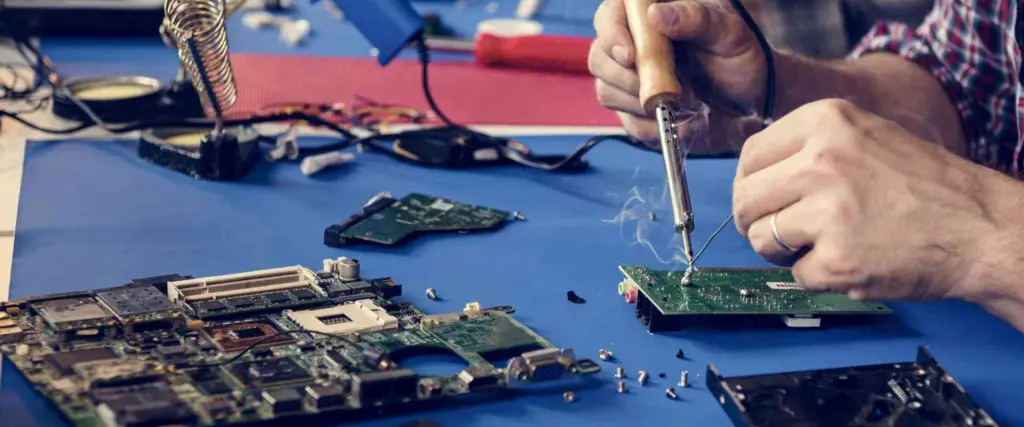
Technicians place specific electronic components onto a new circuit board. They then solder these components to keep the print circuit board together permanently.
From cellphones to kitchen ovens, a lot of consumer devices use PCBs. It is the job of a technician to:
Interpret circuit schematics
Construct PCBs that provide user-defined functions
The end product is what you use in your day-to-day devices.
However, consumers cannot get their PCB directly from the technician. And that is where a shipment specialist comes in.
A Shipment Specialist Gig
Shipment specialist package PCB for, you guessed it, shipment. They wrap PCBs in packaging that’s static resistant, which protects the PCB from both electrical and physical damage.
The shipment specialist’s job is crucial as any PCBs that incur damage during shipment must be recycled or discarded. Unfortunately, these two processes, recycling and discarding, incur extra costs to the manufacturer. Thus the manufacturer tries as much as possible to minimize shipment damages.
Moreover, goods that incur damage during transportation are of no use to the consumer. Therefore, they cannot pay for them; this adds to the net loss due to bad shipment.
However, some customers fake good damages to avoid paying for PCBs. So, how can we deal with this case? That is where the inspector comes in.
The inspector’s gig
Before initializing the shipment process, the inspector must visually inspect the PCB to ensure that they are in good condition. They then have to test the PCBs to ensure they function properly. The inspector inserts the PCB inside a “test fixture” and then powers it to test each function. However, because PCB production happens in bulk, testing each PCB becomes pretty much impossible. They hence select some PCB samples, test them, and then make their conclusion.
And those are some of the jobs you can score having PCB assembly knowledge.
Conclusion
PCBs are a great part of technology; therefore, if you love tech, you will probably love PCB assembly jobs. The jobs come in many different variations; all meant to assemble a PCB to completion and deliver it to the consumer. Each job is unique in its own way; you can hence look for one specific area, major in it, and become a pro to start earning big.
Shengyi PCB materials have been existing for a while now. These materials provide an effective solution to PCB fabrication issues. With the advancement in technology, there is a high need for high performance PCBs. With the right material a high performance and high end PCB can be fabricated.
Also, the properties of a PCB material will determine its performance. Therefore, it is important to use the right PCB material for fabricating your boards. In this article, we will be discussing the Shengyi 1600 PCB material and its properties.
What is Shengyi S1600?
Shengyi S1600 is a conventional FR4 PCB material. This laminate features great properties like great tracking resistance and UV blocking. It functions as the base material for a printed circuit board. This PCB base material is ideal for fabricating high end PCBs. Also, this board features properties like high tensile strength and high temperature resistance.
Shengyi 1600 has got great features which include:
UV blocking
This conventional FR-4 PCB material is great at blocking UV rays from the PCB. Therefore, it protects a circuit board from the impact of UV rays.
Great tracking resistance
The comparative tracking index (CTI) of Shengyi S1600 PCB material is ≥ 600V. CTI describes the leakage current resistance of base material of a PCB. The CTI value specifies Shengyi S1600 resistance against ecological impacts like moisture. Also, this value evaluates the proportionate resistance of Shengyi S1600.
Good PCB Processability
Shengyi S1600 PCB material features great PCB processability. Also, this means that this base material is ideal for PCB manufacturing.
The Mechanical and Thermal Properties of Shengyi S1600
Shengyi S1600 has great thermal and mechanical properties. Each of these properties contributes to the performance of ShengyiS1600.
Low glass transition temperature (tg)
The glass transition temperature of Shengyi S1600 is 135 degree Celsius. This means that at 135 degree Celsius, the temperature of Shengyi S1600 will transform from hard to soft. A PCB base material with this Tg value provides great insulation and low water absorption rate.
Coefficient of thermal expansion (CTE)
The coefficient of thermal expansion measures the changes in the size of a material in response to varying temperature. The CTE (Z axis) of Shengyi S1600 is 55 ppm/℃ before glass transition temperature. After Tg, the CTE is 308 ppm/℃.
Decomposition temperature (Td)
Td describes the temperature at which Shengyi S1600 decomposes chemically. The Td of Shengyi S1600 is 310 degree Celsius at 5% weight loss. When a material goes beyond its Td value, changes to its properties are irreversible.
Thermal stress
This refers to mechanical stress caused by temperature change of a material. This helps to create a relative ability of PCBs to withstand the thermal excursions related to rework and assembly. Also, the thermal stress of Shengyi S1600 is >100S at 288 degree Celsius.
Flexural strength
This describes the ability of a PCB material to resist breakage during bending stress. Also, it specifies how Shengyi S1600 resist bending deflection during energy application to the PCB. Therefore, the flexural strength of Shengyi S1600 is 550 MPa.
Peel strength
This evaluates the adhesive strength of materials bonded together. Also, it describes the ability of Shengyi S1600 to resist forces that can peel it apart. The peel strength of Shengyi S1600 is 1.8 N/mm after thermal stress at 288 degree Celsius.
Shengyi S1600 provides several benefits. Due to the benefits, this laminate is widely used in PCB fabrication. Below are the benefits of Shengyi S1600
Very durable
Shengyi S1600 PCB material is very durable. Also, this PCB base material can withstand environmental conditions. They have great thermal properties which enable them to tolerate heat or moisture.
Used in wide range of applications
This is another benefit of the Shengyi S1600. Also, you can use this PCB material in a wide range of applications. Also, it can perform differently in several applications. Therefore, it is a part of a PCB with several functions.
Easy to design
It is very easy to design this PCB base material. Therefore, you can work with different designs that suit your application requirement.
Great mechanical and thermal properties
Shengyi S1600 has great thermal and mechanical properties. For instance, the CTE and decomposition temperature of this material is excellent. Also, these properties have a great impact on the performance of the PCBs.
Limitations of Shengyi S1600
Irrespective of the benefits of Shengyi S1600, this material has its downsides.
The solder mask on a circuit board shields the circuit from any form of corrosion. Also, it prevents the formation of unwanted bridges between elements. Furthermore, Shengyi S1600 isn’t ideal for solder mask rework. When a solder mask damages during or after manufacturing, there is need for repair. However, Shengyi 1600 doesn’t allow solder mask rework.
Not ideal for anti-CAF application
A PCB that is resistant to CAF is anti-CAF. Conductive anodic filament (CAF) is the formation of a metallic filament from an electrochemical migration process. Also, CAF can lead to failures in PCB. Shengyi S1600 is not ideal for anti-CAF applications.
Shengyi S1600 is ideal for fabricating PCBs used for consumer electronics. Also, you will find this laminate in consumer electronics like refrigerators, television, and more.
Power base board
This PCB material is ideal for designing power base boards. Due to its great mechanical and thermal properties, it is a right option for power base boards.
This is a flat panel display technology commonly found in computer monitors and TVs. Also, Shengyi S1600 is widely used for designing LCD. This device uses liquid crystals to generate an image. Also, you can find it in mobile phones.
Power delay product (PDP)
Shengyi S1600 is vastly used for PDP applications.
Conclusion
Shengyi S1600 PCB material is an efficient base material for fabricating circuit boards. This laminate features excellent thermal and mechanical properties. Also, it has great benefits. Therefore, this article has provided vital information you need to know about Shengyi S1600.
“Nelcote E-720 Epoxy Prepreg, 581 Quartz Reinforced” is fiberglass. It is a two-part epoxy resin material that consists of stiffenings in the form of fibers and a hardener. This material is most often helpful in manufacturing composite parts for industrial purposes, but it has also been beneficial in automotive applications. Unfortunately, the material is not suitable for direct exposure to sunlight as it will lose its mechanical and physical properties.
It is not uncommon for aircraft and other vehicle manufacturers to use this material to manufacture their parts. This material has found the most success in manufacturing aircraft, such as those used by Rayming PCB & Assembly. It has also been helpful to manufacture orthopedic implants, boats, automobile items such as clutch facings, and various other items.
Physical properties
The physical properties of this material are typical for composite material. The density of the material is in the range of 1.5 to 1.8 grams per cubic centimeter (g/cm3) and has low thermal expansion. This means that it will expand or contract less than other materials when subjected to thermal changes, making it highly resistant to thermal stresses. The material’s glass fabric, fibers, and epoxy matrix set the thermal expansion.
The mechanical properties are also fairly typical, with a tensile strength in the range of 8 to 10 gigapascals (GPa), a compressive strength in 9 to 10 GPa, and a flexural modulus close to 500 GPa. These properties make working with and easy on tools when machining and shaping it. In addition, it has good wear resistance and good dimensional stability.
Electrical properties
The electrical properties are non-existent. The material is electrically conductive but is not a good insulator. Therefore, we cannot use it in requiring electrical insulation.
Chemical Properties
The chemical resistance of this material is fairly poor, and we should not use the material should remain in these conditions. At elevated temperatures, it will react with various chemicals, including mild acids, sodium hydroxide, and water. Therefore, we should use it in a controlled environment and appropriate measures to prevent exposure to chemicals, moisture, and other harmful substances.
As stated above, this material is not suitable for use in direct sunlight. It will lose its mechanical and physical properties after only a short exposure period. It is also highly susceptible to moisture absorption. The fiberglass will absorb as much as 20% of its weight in water after only 24 hours of exposure. Therefore, we should not store the material in a dry location with low relative humidity.
As a fibrous material, this material will produce health hazards during its processing and handling. The fibrous materials can become airborne and irritate the respiratory tract, so all personnel who contact this material must wear respiratory protection rated for nuisance dust. The workers should also wear eye protection and gloves to prevent any skin contact with the material.
The manufacturing process for producing this material is fairly simple. First, we process and mill the raw material to produce fiberglass. Next, we extrude this fiberglass through a die and then cured in a closed oven. The fibers are then stretched in a mold, resulting in the part’s final shape.
This material can be challenging, but the correct tools can make it easier.
The processing of this material is straightforward. The raw material is ground and milled in a rotary tool. We should accurately measure the module we are going to use. The part should have a significant amount of bimorphism, meaning that there will be more variation in strength along the X direction than along the Z direction. This gives the technicians more control over how easily the part will successfully deform in bending applications.
The fibrous component of the material is extruded through a die and then cured in a closed oven. This part of the processing will determine how easily the part will bend when the true stresses are applied. The fibers are then stretched in a mold and exothermically cured to cure the resin.
After being processed, you need to select this material for your application. We can use it for many applications, but you must make certain considerations.
Uses of Nelcote E-720 Epoxy Prepreg, 581 Quartz Reinforced
The first consideration is the final shape of the part. The part must be in a predetermined shape before it is processed. In addition, the part must be as symmetrical as possible and have as even a surface finish as possible. This will help ensure that the material will process correctly with little to no warpage and low variation in strength.
We should also determine the type of load imposed on the part. When we fly the part, it will be subject to a certain weight from the aircraft itself and its people. When used in a structural application on buildings, bridges, or other structures that need support, the part must be suitable for the exact amount of stress.
1. Composite parts
The best use for this material is to make composite parts. These are almost always stronger than their composites parts counterparts made with aluminum alloys because they have much higher resistance to deformations. Composites can withstand more strain before breaking and recover from deformation more quickly than their counterparts. This makes the parts more resistant to fatigue, which is the reason for failure in many parts. Composite parts also have more excellent resistance to impact than traditional aluminum alloys. This can be very important when the part could potentially be dropped or impacted.
2. Fairings
Another excellent application for this material is to make fairing parts. The best example of this is aircraft parts. These components must fit perfectly onto the aircraft’s body but do not require any strength or durability. The material can also be helpful for radar and radio antennas and movable horizontal surfaces like those on an airplane tail.
3. Inlet Ducts
Another application for this material is to make inlet ducts. The best use of this material would be to make parts used in engines and other machinery. The material is lighter than aluminum alloys and can allow the part to vibrate less, reducing the noise produced by the machinery.
4. Nacelles
The final application for this material would be to make nacelles for aircraft. Nacelles are a part of the aircraft that can significantly affect the performance of a plane. They consist of parts that we will not expose to any harsh conditions, as they are away from other components. The best use of this material is to make components that cannot vibrate, reducing the amount of noise produced by the machinery.
The final application for this material would be to make radomes. The radomes help to resist the impact of the space around a satellite, allowing the satellite to operate in an environment that can produce high winds. This helps to protect equipment from damage or erosion.
6. Secondary Aircraft Structures
The final application for this material would be to make parts used in secondary aircraft structures. These parts include struts and tails that do not require much strength or support but still must withstand the forces of flight.
Conclusion
Nelcote E-720 is an excellent material used for many different applications. The material has very strong fibers and provides excellent resistance to impact and vibration. The best aspect of this material is that it can be helpful in various environments, including those exposed to the elements or harsh chemicals.
The best use for this material is to manufacture composite parts. These parts give the greatest resistance to fatigue and impact because they can recover from strain much faster than their aluminum counterparts.
Epoxy is a family of cured end products or basic components of epoxy resins. When it is in its liquid form, it can infuse, coat, and laminate materials such as carbon and wood to provide:
Waterproofing
Strength
Durability
After drying the epoxy, it becomes a resin that provides many benefits to various components, especially PCBs. However, there are many epoxies in the market today, each bearing different benefits and applications. We shall hence look at the Nelco N4000-7 EF Halogen-Free Epoxy. An epoxy that is not just efficient but also environmentally friendly.
About the Nelco N4000-7 EF Halogen-Free Epoxy
The Nelco N4000-7 EF Halogen-Free Epoxy is an eco-friendly epoxy that offers CAF resistance for:
Features of the Nelco N4000-7 EF Halogen-Free Epoxy
The Nelco N4000-7 EF bears the following features:
Outstanding thermal stability and moisture resistance
The Nelco N4000-7 EF is compatible with lead-free assembly for designs that have a high layer count. The design is also environmentally conscious for high-reliability applications.
The low moisture intake makes this epoxy reliably during the solder reflow process. It also comes in handy during the repair procedure.
Electrical values that are not compressed
When it comes to electrical performance, this epoxy has no compromises. It eliminates bromine, making it more efficient when you compare it with other bromine components.
Also, if you compare this epoxy with other FR-4 standard loss epoxy systems, you will note that it has superior electricity performance.
Halogen Free
The Nelco N4000-7 EF provides a halogen-free and lead-free solution. It is hence eco-friendly.
CAF resistance
CAF resistance plus low Z-CTE offers a prolonged reliability rate for complex design using:
The Nelco N4000-7 EF has the following electrical properties:
Volume resistivity – as per volume resistivity, the Nelco N4000-7 EF takes on the following values:
1.00e + 13 ohms-cm (C-96/35/90)
1.00e + 13 ohms-cm (E-24/125)
Surface resistance – the surface resistance of the Nelco N4000-7 EF is as follows:
1.00e +12 ohms (C-96/35/90)
1.00e + 12 ohms (E-24/125)
Dielectric constant – the dielectric constant of the Nelco N4000-7 EF is as follows:
At a frequency of 1.00e + 10 Hz, the dielectric constant stands at 3.8 (spit post cavity)
At a frequency of 1.00e + 9 Hz, the dielectric constant hits 4.0 (RF impedance)
When the frequency is set to 1.00e + 6 Hz, the dielectric constant hits 4.1
Dielectric strength – the dielectric strength of the Nelco N4000-7 EF stands at:
39.4 kV/mm
Dielectric Breakdown – the dielectric Breakdown of the Nelco N4000-7 EF is:
>=50000 V
Dissipation factor – the dissipation factor of the Nelco N4000-7 EF is as follows:
At a temperature of 1.00e + 6 Hz, the dissipation factor is 0.013
When you turn up the frequency to 1.00e + 10Hz, the dissipation factor hits 0.016
Arc resistance – The arc resistance of the Nelco N4000-7 EF is:
158 seconds
Descriptive properties of the Nelco N4000-7 EF
The Nelco N4000-7 EF bears the following descriptive properties:
Methylene chloride resistance – Nelco N4000-7 EF epoxies have a methylene chloride resistance of:
0.02
T260 (minutes) – The T260 of the Nelco N4000-7 EF is:
> 30
T288 (minutes) – the T288 of the Nelco N4000-7 EF lies between:
2-4
Z-axis expansion (in percentage) – The Nelco N4000-7 EF has a Z-axis expansion of:
3.5 (500C to 2600C)
Conclusion
The Nelco N4000-7 EF Halogen-Free Epoxy has no halogens, and it supports lead-free assembly. These two features make the Nelco N4000-7 EF Halogen-Free Epoxy environmentally friendly. Therefore, if you are all about a greener future, you will love this epoxy. What’s more, it has CAF resistance and CTE, which boosts its durability. Therefore, when you utilize this epoxy, the final product will ultimately have a longer life span. Hence, if you are looking to save the planet and develop quality, you should try out this excellent epoxy.
Printed circuit boards are a core part of electronic devices. This board serves as the foundation of most electronics. Also, it determines the functionality of devices. Therefore, it is crucial to utilize high-quality material for its manufacturing.
PCB manufacturing involves the use of several materials. However, PCB laminates is the basic raw material used in fabricating PCBs. The Arlon 33N is one of the most efficient polyimide materials for PCB fabrication. This article focuses on Arlon 33N and how it impacts PCB manufacturing.
Arlon 33N PCB material is a polyimide material that imitates the high reliability and performance features of 31N. This PCB material is a UL 94 V-0 polyimide and prepreg system. Also, this material combines the high performance characteristics of polyimide with flame retardance. In addition, this material features the strength of Arlon 31N and 76N. With its flame retardant properties, this material meets the requirements of UL94 V-0.
The resin system is polyimide that features low Z-axis expansion throughout severe thermal excursions. Therefore, this offers plated through-hole integrity. Arlon 33N is much tougher than conventional polyimide. Also, this material is less vulnerable to fracture during profiling and hole drilling. Arlon 33N is another safe PCB material. This material features carcinogenic materials. Therefore, it has no MDA.
This high Tg PCB laminate reduces risk of latent PTH defects. Arlon is a well-known PCB laminate manufacturer. Therefore, this material was specifically designed for use in high performance PCB applications. Also, due to the features and benefits of this material, it is widely used across diverse applications.
Arlon 33N features properties that contribute to its high performance and reliability. Therefore, it is important to know these properties.
Thermal property
The decomposition temperature of this material is 353 °C. However, the Td value at 5% weight loss is 389 °C. This high Td value contributes to the thermal reliability and performance of this material.
Arlon 33N features an exceptional glass transition temperature (Tg). The Tg value is greater than 250 °C at TMA.
The Z-axis CTE of this material is 53 ppm/°C below Tg. When it is above Tg, the Z-axis CTE is 164 ppm/°C. Also, the Z-axis CTE is very low. Therefore, this provides more benefits when used in PCB fabrication.
The dielectric constant of this material is 4.25 at 1 MHz. This is a very high dielectric constant.
This material features a very low dissipation factor (Df). The Df is 0.01 at 1MHz. This means that it doesn’t absorb or discharge heat easily. Arlon 33N is a good insulator. Therefore, it is ideal for high thermal applications.
The volume resistivity of Arlon 33N at (C96/35/90) is 7.2 x 10⁷ MΩ-cm. Also, the volume resistivity at (E24/125) is 4.5 x 10⁸ MΩ-cm.
The surface resistivity of this material at (C96/35/90) is 4.1 x 10⁸ MΩ-cm. Also, the surface resistivity at (E24/125) is 1.6 x 10⁹ MΩ-cm.
Mechanical property
The water absorption rate is 0.21%. This rate is very low. Therefore, Arlon 33N PCB material restricts the amount of water a circuit board will absorb. Therefore, this material is suitable for PCB manufacturing.
The peel strength to copper at elevated temperatures is 7.2 (1.2) Ib/in (N/mm). Also, the peel strength to copper after process solutions is 7.5 (1.3) Ib/in (N/mm).
Ensure you adjust dwell time during the oxide bath. This will help to provide uniform coating.
Bake the inner layers within 107 -121 degrees Celsius before lay-up. Also, bake in a rack for 60 minutes.
Use alkaline permanganate to desmear with settings ideal for polyimide. However, plasma desmear is better for positive etchback.
Arlon 33N is compatible with conventional plating processes.
You can use standard profiling parameters. However, it isn’t advisable to use chip breaker style.
Bake at 121 degrees Celsius before solder reflow of HASL.
Advantages of Arlon 33N PCB Material
This PCB material provides a lot of benefits when used in PCB fabrication.
Low Z direction expansion
Arlon 33N PCB material features low z-expansion. This helps to enhance the reliability of plated through-hole on higher layer count multilayer PCBs. Also, it improves through-hole reliability in applications that require thick PCBs for mechanical purposes. This feature reduces PTH defects risk caused during device attachment and solder reflow. Also, the low Z-axis expansion enhances the reliability of via in thermal cycling conditions.
Excellent copper peel strength retention
The copper peel strength retention of this material is very high. Also, this enables multiple rework cycles and soldering. Therefore, this is suitable in applications that require field repairs.
Industry approval
Arlon 33N PCB material adheres strictly to industry standards. The mechanical and electrical properties of this material meets the requirements of IPC-4101/41 and /40. In addition, it meets the requirements of UL94 V-0 flammability and RoHS.
Environmentally friendly
When environmental safety is a crucial factor, Arlon 33N is the right material to use. This material doesn’t contain any MDA. The non-MDA chemistry helps to resist drill cracking. Also, there are no carcinogenic materials in it. It is bromine and lead-free. Therefore, it is safe for humans and their environments.
Arlon 33N provides high thermal resistance for very high temperature burn-in applications. This is because of the use of pure polyimide in this material. Also, Arlon 33N is a high thermal material reliable for high temperature environments.
The automotive and transportation industries require the use of high performance PCB material. Arlon 33N PCB material is widely used in powertrain and UTH. Also, you will find this material useful in designing exterior and interior parts of automobiles. It plays a critical role in designing under-hood automotive controls.
Electrical and electronics
You will find these PCB materials in parts and components of electrical devices. Also, you will find them in consumer electronic devices.
Industrial
Arlon 33N PCB material is useful in designing some industrial electronic devices. The industrial system is exposed to high temperatures. Therefore, the use of high thermal PCBs is advisable.
Conclusion
This article has explained everything you need to know about Arlon 33N. This PCB material offers a lot of benefits and features.