
RAYPCB · ENGINEERING GUIDE
Arlon 47N: Low-Flow Epoxy Heat-Sink Bonding
Arlon 47N is a low-flow epoxy prepreg used for controlled bonding, including rigid-flex regions and heat-sink attachment. Its engineering task is to form a suitable bond within the thermal and geometric limits of the adjacent materials. It should not be presented as a universal high-conductivity thermal interface material.
This page follows the heat-sink bondline and its limitations. The Arlon material hub provides the broader family selection.
Keep the lower-temperature bonding context explicit
The official 47N sheet describes a tetrafunctional modified epoxy system with Tg 130°C and an optional reduced lamination-temperature route. It cites IPC-4101/21 modified for low flow. The optional route and the normal process guidance should not be collapsed into one universal cure setting.
The adjacent board, heat sink and any already-mounted components can impose different limits. The responsible manufacturing team must qualify the actual process. A low cure-temperature option is not proof that every assembled board can safely undergo the proposed bonding cycle.
Evidence and construction decision
| Item | Source or model boundary | Action for the design review |
|---|---|---|
| Form | 47N low-flow epoxy prepreg | Bonding material, not a qualified thermal interface. |
| Tg | 130°C typical | Different from 49N and 51N. |
| Cure guidance | Reduced and normal routes differ | Qualified manufacturing instructions govern the build. |
Define both the mechanical bond and the thermal path
Show the metal type, surface condition, flatness, bond area and target separation. Identify whether the heat source covers the full bond area or a small local region. Electrical insulation and mechanical attachment may remain important even when heat transfer is the main objective.
Voids, surface preparation and local pressure can affect the finished bond. The material name does not communicate an acceptable void criterion or a completed thermal resistance. Put those requirements in the drawing and evidence plan.
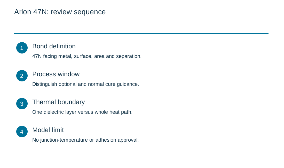
| Review item | What to establish |
|---|---|
| Bond definition | 47N facing metal, surface, area and separation. |
| Process window | Distinguish optional and normal cure guidance. |
| Thermal boundary | One dielectric layer versus whole heat path. |
| Model limit | No junction-temperature or adhesion approval. |
Use a one-dimensional resistance model as a limited illustration
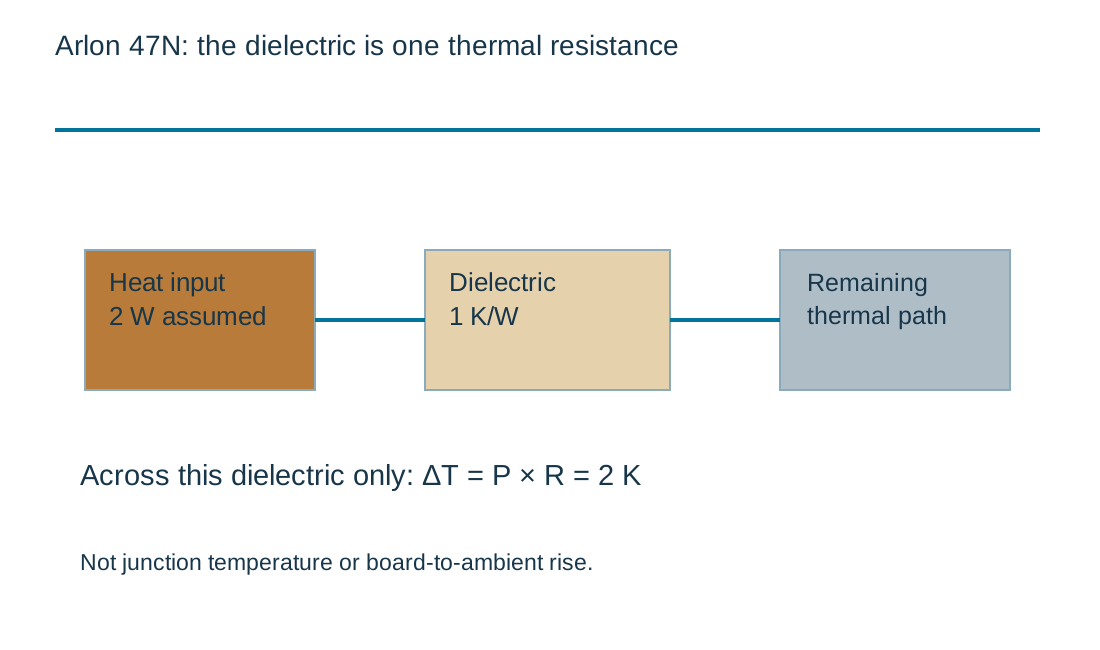
The tool calculates R = t/(kA) for one uniform dielectric layer. With hypothetical thickness 100 µm, conductivity 1 W/(m·K) and area 100 mm², the resistance is 1 K/W. At 2 W through that layer, the across-layer temperature difference is 2 K.
Those inputs are not 47N specifications. The model excludes spreading, interfaces, copper, heat-sink geometry and ambient conditions. It does not calculate junction temperature or authorize a working voltage. Use measured or controlled material data before applying the arithmetic to a real bond.
IMS dielectric thermal-resistance illustration
IMS dielectric thermal-resistance illustration
Use the current inputs and keep the assumptions
Start with the example only to inspect the units and the calculation boundary. Replace every assumption with a value tied to your own document or measurement. An empty numeric field is not zero. The review-reference field is a local label; avoid entering customer names, confidential part numbers or other private information into a public worksheet.
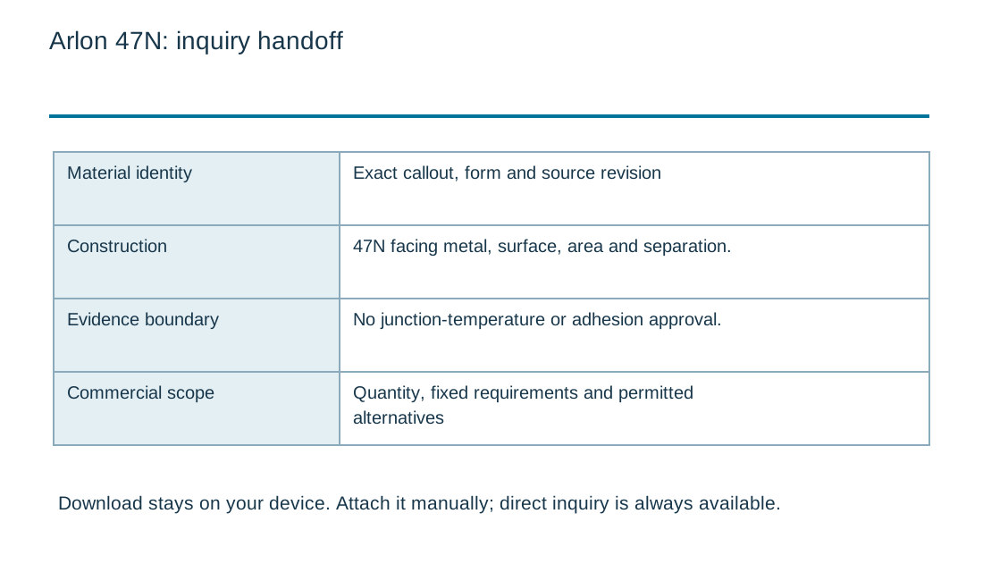
After calculating, read the notes alongside the numerical result. Changing any input invalidates the displayed result and disables its download until you calculate again. For a comparison, keep the units, geometry, material condition and measurement boundary consistent. A long decimal result does not imply equally precise input data. The downloadable record stays on your device and can be attached manually to an inquiry. It is not automatically transferred into the Contact form.
If an input is unknown, identify the person or document needed to resolve it. Do not fill a gap with a favorable generic value simply to obtain a result. You can request a material or fabrication review without using the tool. The arithmetic illustrates a relationship; it does not accept a construction, certify a material, establish current pricing or replace a supplier process specification.
| Input | What to establish before using it |
|---|---|
| Review reference | Nonconfidential revision label. |
| Dielectric thickness · µm | Actual insulating layer only, excluding copper and aluminium. |
| Through-thickness conductivity · W/(m·K) | Hypothetical value; replace with exact grade and method. |
| Uniform heat-flow area · mm² | Ideal common area through the insulating layer; no spreading. |
| Heat through this layer · W | Allocated steady heat flow, not total electrical input power. |
Optional cost comparison from your own allowances
Use a quotation or a clearly labeled internal assumption for each input. Keep the quantity, construction and inspection scope the same when comparing alternatives. This uncalibrated planning model adds entered values; it contains no current market rates and does not issue a RAYPCB quotation. You can contact the team without completing it.
Optional project allowance comparison
Compare higher-temperature bonding routes when required
49N and 51N address different epoxy low-flow contexts. Review the required bond geometry, assembly sequence and adjacent-material limits before proposing a change. A higher Tg alone does not prove better adhesion or lower thermal resistance.
If the challenge is filling thick copper or metal-core clearances with polyimide, 84HP is a separate material task. Do not substitute it solely because a drawing contains both a heat sink and thick copper.
Keep process details out of unsupported web shortcuts
The public 47N sheet includes an availability table with 85N-prefixed entries and an inconsistent drill-size unit presentation. Clarify the actual ordering and process documentation with the supplier. Do not derive a material code or machine setup from an ambiguous public table.
Agree which evidence demonstrates bond quality: representative cross-section, thickness, adhesion or thermal measurements as appropriate to the requirement. A single favorable material number cannot replace that finished-interface evidence.
Request a heat-sink bonding review with comparable cost inputs
Send the exact grade, facing materials, geometry, surface condition, thermal requirement, electrical insulation requirement and permitted process window. Include quantity, assembly state and inspection scope. Identify any component that cannot tolerate the proposed exposure.
The optional allowance tool adds user-entered values only. It has no current 47N price or qualified thermal model. The next useful step is a proposed bond construction and verification plan, with open questions visible before production release.
Review supplied form, local geometry and process together
A stackup is an agreement about physical construction, not just a vertical list of copper layers. Give each dielectric interval an identity and distinguish cured core thickness from the pressed thickness of bonding material. State whether copper is included in every quoted dimension.
Review the implications of a material change across impedance, lamination, drilling, registration and assembly exposure. A replacement with a similar headline Tg or Dk can still require a different geometry or process. Preserve the approved layer order, copper distribution assumptions and measurement basis with the manufacturing files.
Use the worksheet to organize a review, then obtain the fabricator's proposed construction and tolerances. Close differences before release. The final stackup, drawing and procurement material list should reference the same revision, especially when multiple suppliers or repeat orders are involved.
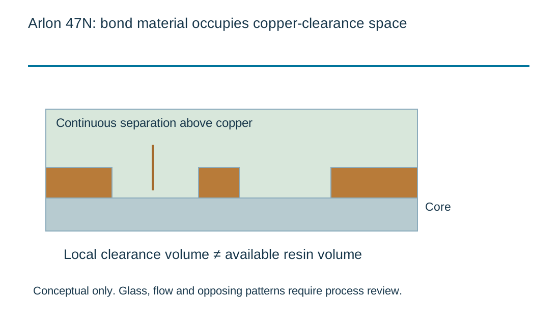
Bonding materials cannot be selected from a cured-laminate table alone. Establish whether the product is woven-glass prepreg, another reinforced bonding system or resin-coated copper. Each form has a different relationship between its supplied condition and the finished dielectric interval. Preserve the exact product and source revision in the proposed build.
Local copper distribution matters. Average coverage can conceal a large clearance region, a thick copper transition or a difficult target area. Supply the actual artwork and identify the locations that drive filling, registration or opening requirements. A single global thickness or aspect ratio does not characterize every local feature.
Process guidance should be applied by the responsible manufacturing team to the actual construction. A public document does not replace press-load qualification, handling controls or an approved drilling and metallization route. Do not use a generic bake or cure instruction for an unidentified bonding material.
Agree how the critical features will be verified. Representative cross-sections, dimensions and appropriate electrical or reliability evidence answer different questions. Keep the selected locations and acceptance requirements with the drawing so that a successful easy region is not mistaken for evidence about the most demanding feature.
Standards, source context and limits
Use the edition, amendment and material-document revision named in the purchase agreement. A standards title, marketing label or supplier product family does not establish that a particular lot meets a requirement. Public summaries are useful for scope; the controlled specification and applicable test method govern acceptance.
The examples on this page are illustrative engineering scenarios. They are not RAYPCB production records or guaranteed material values. Source links identify the organizations responsible for the referenced information. Confirm applicability to the exact grade, construction and test condition before carrying a number into a drawing or qualification report. Sources were reviewed on 3 October 2026. A public catalog search is not proof that an unlisted product never existed. Where the exact designation or current technical sheet could not be verified, this page provides a clarification workflow rather than an invented material specification. Current supply, construction availability and qualification remain separate questions.
For fabrication scope and the agreed construction requirements, see PCB manufacturing.

