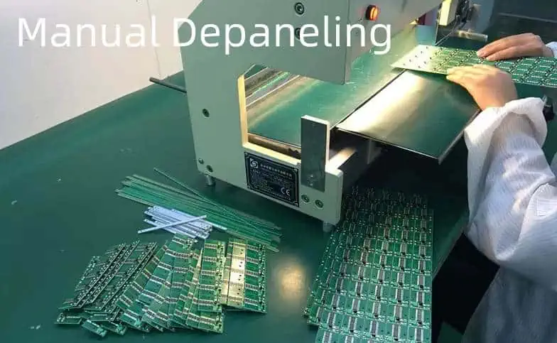
Laser depaneling is a cutting-edge technology that uses a focused laser beam to separate individual PCBs from a larger panel. This method offers numerous advantages over traditional mechanical depaneling techniques, especially when dealing with delicate or uniquely shaped PCBs like round ceramic boards.
The Science Behind Laser Depaneling
Laser depaneling works on the principle of material ablation. The laser beam, typically a CO2 or UV laser, is focused on the PCB material, vaporizing it along a predetermined path. This process creates a clean, precise cut without applying mechanical stress to the board.
Key Components of a Laser Depaneling System
Laser Source
Beam Delivery System
Motion Control System
Vision System
Exhaust and Filtration System
Advantages of Laser Depaneling for Round Ceramic PCBs
Precision: Laser cutting offers unparalleled accuracy, crucial for round shapes.
Stress-Free: No mechanical stress is applied to the delicate ceramic material.
Clean Cuts: Laser cutting produces smooth edges without debris.
Flexibility: Easily adaptable for various board shapes and sizes.
Programmability: Can be quickly reprogrammed for different designs.
Preparing for Laser Depaneling of Round Ceramic PCBs
Material Considerations
Ceramic PCBs have unique properties that make them ideal for certain applications but also require special handling during the depaneling process.
Development of more efficient and powerful laser sources
Advancements in automated handling and inspection systems
Conclusion
Laser depaneling of round ceramic PCBs represents a significant advancement in PCB manufacturing technology. By offering precision, flexibility, and stress-free separation, it enables the production of high-quality, complex PCB designs. As the electronics industry continues to demand more sophisticated and compact designs, the role of laser depaneling in PCB manufacturing is set to become increasingly important.
FAQ
Q1: Is laser depaneling suitable for all types of ceramic PCBs?
A1: While laser depaneling is suitable for most ceramic PCBs, the specific parameters may need adjustment based on the type of ceramic material, thickness, and board design. It’s particularly effective for round ceramic PCBs due to its precision in cutting curved paths.
Q2: How does the cost of laser depaneling compare to traditional methods?
A2: Initially, the setup cost for laser depaneling can be higher than traditional methods. However, it often proves more cost-effective in the long run, especially for high-volume production or when working with complex or delicate designs like round ceramic PCBs.
Q3: Are there any limitations to the thickness of ceramic PCBs that can be laser depaneled?
A3: While laser depaneling can handle a wide range of thicknesses, extremely thick ceramic PCBs may require multiple passes or a combination of techniques. The maximum thickness depends on the power of the laser and the specific properties of the ceramic material.
Q4: How does laser depaneling affect the electrical properties of ceramic PCBs?
A4: When done correctly, laser depaneling has minimal impact on the electrical properties of ceramic PCBs. The heat-affected zone is typically very small, and the process doesn’t introduce mechanical stress that could affect the board’s performance.
Q5: What maintenance is required for a laser depaneling system?
A5: Regular maintenance of a laser depaneling system typically includes cleaning of optics, checking and replacing filters, calibrating the laser and motion control systems, and inspecting for any wear or damage to components. The frequency of maintenance depends on usage but is generally less intensive than mechanical depaneling systems.
Analog signals form the foundation of countless electronic systems, from precision sensors to high-fidelity audio equipment. However, these signals are particularly vulnerable to noise interference, which can severely impact performance and accuracy. This comprehensive guide reveals proven strategies to eliminate noise in PCB analog circuits and achieve optimal signal integrity.
Understanding Analog Signal Noise
What Is Analog Signal Noise?
Noise represents any unwanted electrical interference that corrupts your desired signal. Unlike digital systems that can tolerate some distortion, analog circuits require exceptional signal purity for accurate operation. Even minimal noise can cascade into significant performance degradation.
Types of Analog Signal Noise
External Noise Sources:
Electromagnetic interference (EMI) from radio frequencies
Noise contamination results in several critical issues:
Signal-to-Noise Ratio (SNR) Degradation – Reduces the system’s ability to distinguish meaningful signals from background interference, directly affecting measurement precision and dynamic range.
Measurement Accuracy Loss – Particularly devastating in sensor applications where small signal changes carry important information. Even minor noise can mask critical data or introduce false readings.
Communication Errors – In analog communication systems, noise increases bit error rates and reduces effective transmission distance and data rates.
Dynamic Range Limitations – Noise floor elevation reduces the usable signal range, forcing designers to use higher signal levels or accept reduced performance.
Common Noise Sources in PCB Design
Electromagnetic Interference (EMI)
EMI represents one of the most challenging noise sources in modern electronics. High-frequency switching circuits, wireless devices, and power electronics create electromagnetic fields that couple into sensitive analog circuits through multiple mechanisms.
Radiative Coupling occurs when electromagnetic waves propagate through space and induce currents in PCB traces acting as antennas. The effectiveness of this coupling depends on trace length, orientation, and frequency.
Conductive Coupling happens when noise travels through shared conductors like power lines, ground connections, or cable shields. This mechanism often proves more problematic than radiative coupling in well-designed systems.
Power Supply Contamination
Modern electronic systems place enormous demands on power supplies, creating various noise mechanisms that directly corrupt analog signals.
Switching Regulator Noise introduces high-frequency ripple and switching transients that can couple into analog circuits through power connections or electromagnetic radiation.
Load Regulation Errors occur when varying current demands cause voltage fluctuations that modulate analog signal references and bias points.
Ground Bounce happens when rapid current changes in digital circuits create voltage variations in the ground system, affecting analog circuit reference levels.
Ground System Problems
Poor grounding practices create some of the most insidious noise problems in mixed-signal systems.
Ground Loops form when multiple return paths exist between circuit sections, allowing noise currents to circulate and create voltage differences between supposedly common points.
Impedance Variations in ground planes cause voltage drops proportional to current flow, creating noise voltages that affect sensitive analog circuits.
Thermal Gradients across large ground planes can create thermoelectric voltages that appear as low-frequency noise in precision circuits.
Crosstalk Mechanisms
Signal crosstalk occurs through capacitive and inductive coupling between nearby conductors, with the coupling strength depending on physical proximity, signal frequencies, and circuit impedances.
Capacitive Crosstalk dominates at higher frequencies and shorter trace separations, where electric field coupling becomes significant.
Inductive Crosstalk affects circuits with larger current loops and becomes more problematic as switching speeds increase.
Essential PCB Layout Techniques
Strategic Circuit Partitioning
Effective noise reduction begins with intelligent PCB layout that separates incompatible circuit functions and minimizes coupling opportunities.
Physical Separation – Position analog and digital circuits on opposite sides of the PCB or in separate board regions. Maintain at least 10mm separation between high-speed digital switching circuits and sensitive analog sections.
Ground Plane Strategy – Implement separate analog and digital ground planes connected at a single star point near the main power supply. This prevents digital switching currents from flowing through analog ground paths.
Power Domain Isolation – Use separate power supplies or carefully filtered power sections for analog and digital circuits. Digital switching creates significant power supply noise that can corrupt analog performance.
Trace Routing Optimization
Proper trace routing dramatically reduces noise susceptibility and electromagnetic emissions.
Minimize Loop Areas – Keep signal and return path loops as small as possible to reduce both magnetic field coupling and radiation. Use ground planes to provide short return paths for all signals.
Controlled Trace Lengths – Keep analog signal traces short and direct. Every millimeter of trace length increases noise pickup and signal degradation potential.
Orthogonal Routing – Route analog and digital traces perpendicular to each other when crossing is unavoidable. This minimizes the coupling area and reduces crosstalk.
Differential Pair Matching – For differential signals, maintain tight coupling between positive and negative traces while ensuring consistent impedance and equal trace lengths.
Ground Plane Design Excellence
A well-designed ground plane serves multiple critical functions in noise reduction.
Solid Ground Coverage – Maintain continuous ground plane coverage under analog circuits without breaks or slots that force current detours. Any ground plane discontinuities create impedance variations and potential noise issues.
Via Stitching – Use multiple ground vias to connect ground planes on different layers, reducing ground impedance and providing multiple return paths for high-frequency currents.
Thermal Management – Consider thermal effects in ground plane design, as temperature gradients can create thermoelectric voltages that appear as noise in sensitive circuits.
Power Supply Noise Mitigation
Advanced Decoupling Strategies
Effective power supply decoupling requires understanding the frequency-dependent behavior of different capacitor types and implementing a comprehensive filtering strategy.
Multi-Capacitor Networks – Use parallel combinations of different capacitor values to address various frequency ranges. Typical combinations include 0.1μF ceramic capacitors for high-frequency decoupling (>1MHz), 10μF tantalum capacitors for mid-frequency range (1kHz-1MHz), and larger electrolytic capacitors for low-frequency supply variations.
Strategic Placement – Position decoupling capacitors as close as possible to IC power pins, minimizing the inductance of connecting traces. Use short, wide traces or direct via connections to reduce parasitic impedance.
ESR Considerations – Select capacitors with appropriate Equivalent Series Resistance (ESR) characteristics for your application. Very low ESR capacitors can cause resonance issues, while higher ESR provides damping but reduces high-frequency effectiveness.
Linear Regulator Implementation
Linear regulators provide superior noise performance compared to switching regulators but require careful implementation for optimal results.
Low-Dropout Regulators – Modern LDO regulators offer excellent noise performance with PSRR (Power Supply Rejection Ratio) exceeding 60dB at low frequencies. Select regulators with high PSRR across your frequency range of interest.
Output Filtering – Add LC filters to regulator outputs for additional noise reduction. Use inductors with appropriate current ratings and low DC resistance to prevent voltage drops.
Thermal Management – Implement adequate heat sinking for linear regulators, as thermal noise increases with temperature and excessive heat can degrade performance.
Switching Regulator Optimization
When switching regulators are necessary for efficiency reasons, specific techniques can minimize their noise impact on analog circuits.
Frequency Planning – Choose switching frequencies that avoid interference with analog signal frequencies. Use spread-spectrum switching when available to distribute noise energy across a wider frequency range.
Layout Isolation – Isolate switching regulator circuits from analog sections using ground plane gaps and physical separation. Shield switching nodes with ground planes to contain electromagnetic emissions.
Post-Regulation Filtering – Follow switching regulators with linear post-regulators or comprehensive LC filters to remove switching noise before supplying analog circuits.
Advanced Grounding Strategies
Star Grounding Implementation
Star grounding provides the foundation for low-noise analog circuit design by eliminating ground loops and minimizing noise circulation.
Single-Point Connection – Connect all circuit ground returns to a single, low-impedance point typically located near the main power supply. This prevents ground currents from one circuit affecting another circuit’s ground reference.
Current Path Analysis – Analyze all current return paths to ensure they flow through predictable, low-impedance routes. High-current digital switching should not share return paths with sensitive analog signals.
Mechanical Considerations – Ensure the star ground point has excellent mechanical and electrical integrity. Use large copper areas or bus bars to minimize resistance and inductance.
Ground Plane Architecture
Modern PCB designs rely heavily on ground planes for both power distribution and noise control.
Layer Stack-up Planning – Position ground planes strategically in the PCB stack-up to provide shielding between signal layers and maintain controlled impedances.
Plane Segmentation – When separate analog and digital ground planes are necessary, carefully plan their connection strategy to maintain low impedance while preventing noise coupling.
Via Management – Use adequate via counts to connect ground planes between layers, with special attention to high-current areas where multiple vias may be necessary to handle current density.
Isolation Techniques
Advanced isolation methods can effectively separate noisy and sensitive circuits while maintaining necessary signal connections.
Transformer Isolation – Use isolation transformers for AC signals or power transfer where complete galvanic isolation is required. Transformers provide excellent common-mode noise rejection.
Optocoupler Implementation – Digital signals can be isolated using optocouplers, breaking ground loops while maintaining signal integrity. Select optocouplers with appropriate speed and noise characteristics.
Capacitive Isolation – AC signals can be coupled through carefully selected capacitors that block DC and low-frequency noise while maintaining signal transmission.
RC Low-Pass Filters – Simple RC filters provide effective high-frequency noise attenuation with minimal component count. Calculate time constants carefully to avoid signal bandwidth limitations.
LC Filter Networks – LC filters offer superior performance for power supply filtering and can achieve higher attenuation rates than RC filters. Consider inductor parasitic resistance and capacitor ESR in performance calculations.
Pi-Section Filters – Multiple-stage filters using pi-section configurations can achieve very high attenuation levels for stubborn noise problems.
Active Filter Solutions
Active filters using operational amplifiers provide greater design flexibility and can achieve complex frequency responses.
Sallen-Key Topology – This popular active filter configuration offers good performance with standard operational amplifiers and provides design flexibility for various filter responses.
Multiple Feedback Designs – Multiple feedback filter architectures can achieve high Q factors and steep roll-off characteristics for demanding applications.
State-Variable Filters – These versatile filters can simultaneously provide low-pass, high-pass, and band-pass outputs from a single circuit.
Differential Signal Processing
Differential signaling provides inherent noise immunity by canceling common-mode interference.
Instrumentation Amplifiers – Purpose-built instrumentation amplifiers offer excellent common-mode rejection ratios (CMRR) exceeding 100dB and provide the foundation for high-performance differential signal processing.
Balanced Line Drivers – Use differential line drivers for signal transmission over longer distances or in high-noise environments. Maintain tight coupling between differential pair traces.
Common-Mode Filtering – Add common-mode chokes to differential signal lines to attenuate common-mode noise while preserving differential signals.
Component Selection Guidelines
Low-Noise Semiconductor Selection
The choice of active components significantly impacts overall system noise performance.
Operational Amplifier Specifications – Prioritize low input voltage noise density (typically <10 nV/√Hz), low input current noise, and high gain-bandwidth product. Consider input bias current requirements for high-impedance sources.
Reference Voltage Sources – Use precision voltage references with low temperature coefficients and noise specifications. Buried zener references typically offer superior noise performance compared to bandgap references.
Analog-to-Digital Converters – Select ADCs with appropriate resolution and sampling rates for your application, considering that higher resolution generally requires better noise performance from preceding circuits.
Passive Component Optimization
Passive components contribute both wanted and unwanted characteristics to circuit performance.
Resistor Technology – Metal film resistors offer lower noise than carbon composition types, while wirewound resistors provide the lowest noise but have parasitic inductance. Consider thermal coefficients for precision applications.
Capacitor Characteristics – Ceramic capacitors provide excellent high-frequency performance but may exhibit microphonic effects. Film capacitors offer better stability and lower distortion for audio applications.
Inductor Selection – Choose inductors with appropriate saturation current ratings and low DC resistance. Toroidal cores generally provide better electromagnetic compatibility than rod cores.
Crystal and Timing Components
Clock sources can contribute significant noise to mixed-signal systems through both conducted and radiated coupling.
Crystal Oscillator Specifications – Low-jitter crystal oscillators reduce phase noise that can affect analog circuit performance. Consider temperature stability and aging characteristics.
Clock Distribution – Use proper clock buffering and distribution techniques to minimize clock-related noise injection into analog circuits.
Frequency Planning – Choose clock frequencies that avoid interference with analog signal frequencies, considering harmonics and intermodulation products.
Shielding and Protection Methods
Enclosure Design Principles
Mechanical enclosures provide the first line of defense against external electromagnetic interference.
Faraday Cage Effectiveness – Metal enclosures create Faraday cages that attenuate external electromagnetic fields. Effectiveness depends on enclosure material, wall thickness, and seam quality.
Aperture Management – Any openings in the enclosure (display windows, connector panels, ventilation) reduce shielding effectiveness. Use conductive gaskets and proper grounding to maintain shielding integrity.
Cable Entry Points – Implement proper cable shielding and filtering at enclosure entry points to prevent noise from entering through cable connections.
Internal Shielding Strategies
Internal shielding can isolate sensitive circuit sections from noise sources within the same enclosure.
PCB-Level Shielding – Use PCB-mounted shield cans over sensitive analog circuits. Ensure proper grounding of shield cans to maintain effectiveness.
Compartmentalization – Design internal enclosure compartments to separate analog and digital circuit sections, using conductive dividers where necessary.
Cable Routing – Route sensitive analog cables away from noisy digital cables and power conductors. Use shielded cables for critical analog signals.
Gasket and Grounding Systems
Proper grounding of shielding systems is essential for their effectiveness.
Conductive Gaskets – Use EMI gaskets at all enclosure seams to maintain electrical continuity and prevent electromagnetic leakage.
Ground Plane Connectivity – Ensure excellent electrical connection between enclosure grounds and PCB ground planes using multiple connection points.
Corrosion Prevention – Use appropriate materials and platings to prevent galvanic corrosion at grounding interfaces, which can degrade shielding effectiveness over time.
Testing and Validation
Noise Measurement Techniques
Proper measurement techniques are essential for characterizing noise performance and validating design improvements.
Oscilloscope Analysis – Use digital oscilloscopes with appropriate bandwidth and sensitivity to measure noise levels. Consider oscilloscope noise contributions when making sensitive measurements.
Spectrum Analyzer Applications – Spectrum analyzers reveal noise characteristics in the frequency domain, helping identify specific noise sources and frequencies.
Network Analyzer Measurements – For AC measurements, network analyzers can characterize transfer functions and identify resonances that may contribute to noise problems.
Signal Integrity Assessment
Comprehensive signal integrity testing ensures that noise reduction efforts don’t compromise signal quality.
Eye Diagram Analysis – For digital signals, eye diagrams reveal the combined effects of noise, jitter, and intersymbol interference on signal quality.
Total Harmonic Distortion – THD measurements quantify the impact of noise and nonlinearity on signal purity, particularly important for audio applications.
Signal-to-Noise Ratio Testing – Direct SNR measurements provide quantitative assessment of noise reduction effectiveness.
Environmental Testing
Real-world performance requires testing under actual operating conditions.
Temperature Variation – Test noise performance across the expected temperature range, as thermal effects can significantly impact noise levels.
Power Supply Variation – Verify noise performance with power supply variations that may occur in actual applications.
Electromagnetic Compatibility – Conduct EMC testing to ensure the design meets regulatory requirements and performs well in realistic electromagnetic environments.
Real-World Case Study
Project Background: Precision Temperature Monitoring System
A medical device manufacturer needed to develop a precision temperature monitoring system capable of 0.01°C accuracy over a -40°C to +85°C range. The initial prototype suffered from significant noise issues that prevented meeting accuracy requirements.
Initial Problem Analysis
Symptom Identification – Temperature readings showed random variations of ±0.5°C, far exceeding the required accuracy. Noise appeared as both high-frequency fluctuations and slow drifts.
Noise Source Investigation – Testing revealed multiple noise sources: switching power supply ripple, crosstalk from nearby digital circuits, and thermal gradients in the PCB ground plane.
Performance Requirements – The system needed to achieve better than 10μV noise performance to meet accuracy goals with the selected temperature sensor.
Solution Implementation
PCB Layout Redesign – Separated the analog sensor circuit to a dedicated PCB section with its own ground plane. Implemented guard traces around sensitive signal paths and minimized trace lengths.
Power Supply Architecture – Replaced the switching regulator with a low-noise linear regulator for the analog section. Added comprehensive decoupling with multiple capacitor values ranging from 0.01μF to 100μF.
Filtering Implementation – Added a two-pole active filter with 10Hz cutoff frequency to attenuate high-frequency noise while preserving the temperature signal bandwidth.
Shielding Enhancement – Implemented a grounded copper shield over the analog section and used a metal enclosure with proper EMI gaskets.
Results and Validation
Noise Reduction Achievement – Noise levels decreased from 50μV RMS to less than 2μV RMS, enabling the required measurement accuracy.
Temperature Performance – Final system achieved ±0.005°C accuracy over the full temperature range, exceeding the original requirements.
Production Considerations – The solution proved manufacturable and cost-effective, with noise performance remaining consistent across production units.
Lessons Learned
Early Design Consideration – Addressing noise issues during the initial design phase proves far more cost-effective than retrofit solutions.
Systematic Approach – Identifying and addressing all noise sources simultaneously provides better results than piecemeal improvements.
Measurement Validation – Comprehensive testing with proper instrumentation is essential for validating noise reduction effectiveness.
Frequently Asked Questions
What’s the most effective single technique for reducing analog signal noise?
Implementing a proper ground plane design typically provides the greatest noise reduction benefit. A solid, continuous ground plane reduces impedance, provides shielding, and eliminates many coupling mechanisms that cause noise problems. However, comprehensive noise reduction requires combining multiple techniques rather than relying on any single approach.
How do I choose between ferrite beads and inductors for noise filtering?
Ferrite beads excel at suppressing high-frequency noise (>1MHz) and provide resistive damping that prevents resonances. Use them for power supply decoupling and digital signal filtering. Inductors work better for lower frequencies and power applications where you need to maintain DC characteristics while filtering AC noise.
Can switching power supplies ever be used in low-noise analog designs?
Yes, but they require careful implementation. Use high switching frequencies (>2MHz) to push noise above analog signal bandwidths, implement comprehensive output filtering, and physically isolate the switching circuits from analog sections. Post-regulation with linear regulators often provides the best compromise between efficiency and noise performance.
How much improvement can I expect from differential signaling?
Properly implemented differential signaling can provide 30-60dB common-mode noise rejection, dramatically improving performance in noisy environments. The improvement depends on maintaining good balance between the differential pair traces and using receivers with high common-mode rejection ratios.
What’s the minimum spacing needed between analog and digital circuits?
Maintain at least 10mm separation between high-speed digital switching circuits and sensitive analog sections. However, physical spacing alone isn’t sufficient – you also need proper ground plane design and power supply isolation to prevent coupling through shared conductors.
How do I measure noise in very low-level analog signals?
Use a spectrum analyzer or low-noise oscilloscope with appropriate input coupling and bandwidth limiting. Ensure your measurement setup doesn’t contribute more noise than the circuit under test. Consider using averaging techniques and proper grounding of measurement equipment.
Should I use separate analog and digital ground planes?
This depends on your specific application. Simple designs often work better with a single ground plane to avoid ground loop issues. Complex mixed-signal designs may benefit from separate planes connected at a single star point. The key is understanding current flow paths and minimizing shared return paths between noisy and sensitive circuits.
What role does PCB material selection play in noise reduction?
PCB dielectric properties affect signal integrity and EMI performance. Low-loss materials reduce signal degradation, while materials with stable dielectric constants minimize variation with temperature and frequency. For most applications, standard FR-4 provides adequate performance when proper design techniques are followed.
How do I handle noise in battery-powered portable devices?
Battery-powered devices have unique advantages (no power line interference) and challenges (limited power budgets). Focus on efficient low-noise regulators, careful power management, and consider that battery impedance can create noise coupling between circuits. Use proper decoupling and consider the effects of battery aging on noise performance.
What’s the best approach for reducing 50Hz/60Hz power line interference?
Implement notch filters tuned to the power line frequency and its harmonics, ensure proper grounding and shielding, use differential signaling where possible, and maintain adequate separation from power conductors. Twisted pair cables and common-mode chokes are particularly effective for this type of interference.
Conclusion
Achieving low-noise analog signal performance requires a systematic approach combining proper PCB layout, component selection, power supply design, and shielding techniques. While noise elimination represents one of the most challenging aspects of analog circuit design, the techniques presented in this guide provide a comprehensive framework for success.
The key to effective noise reduction lies in understanding that noise problems rarely have single causes or solutions. Instead, successful designs address all potential noise sources simultaneously through careful planning and implementation. By following these proven strategies and adapting them to your specific requirements, you can achieve the clean, precise analog signals essential for high-performance electronic systems.
Remember that noise reduction is an iterative process requiring careful measurement and validation at each step. Start with the fundamentals of good layout and grounding, then add filtering and shielding as needed to meet your performance goals. With proper attention to these details, even the most demanding analog applications can achieve excellent noise performance.
Nixie tubes represent a captivating piece of electronic history, offering a warm, vintage aesthetic that continues to fascinate electronics enthusiasts and hobbyists. This comprehensive guide will walk you through creating a Nixie tube clock using a unique freeform wire construction technique that eliminates the need for a traditional printed circuit board (PCB).
Understanding Nixie Tubes
What Are Nixie Tubes?
Nixie tubes are cold-cathode display devices invented in the 1950s, featuring a wire mesh anode and multiple cathodes shaped like numerals. When a specific cathode is energized, it glows with a distinctive orange-red color, creating a mesmerizing display of numbers.
Q1: Is a freeform wire construction as reliable as a PCB?
A: While different, a well-executed freeform construction can be equally reliable. Proper design, soldering, and mechanical support are key to long-term performance.
Q2: How dangerous is the high voltage in a Nixie tube clock?
A: High voltage components require careful handling. Always use proper insulation, avoid direct contact, and implement safety features like current limiting.
Q3: Can I use different types of Nixie tubes?
A: Yes, but ensure compatibility with your power supply and switching circuits. Verify pinout and voltage requirements for each tube type.
Q4: What’s the typical power consumption of a Nixie tube clock?
A: Approximately 2-5 watts, depending on tube type and display duration. Implementing power-saving modes can reduce overall consumption.
Q5: How long do Nixie tubes typically last?
A: Quality Nixie tubes can last 50,000-100,000 hours (5-11 years of continuous operation) with proper care and moderate usage.
Conclusion
Building a Nixie tube clock using freeform wire construction represents a challenging yet rewarding project that combines vintage electronics, precise engineering, and artistic expression. Each step requires careful consideration, technical skill, and creative problem-solving.
The journey of creating such a clock is as valuable as the final product—a testament to the enduring fascination of vintage electronic technologies and the maker’s spirit of innovation.
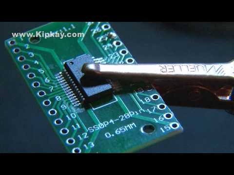
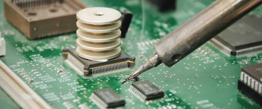
Printed Circuit Board (PCB) chip package soldering is a critical process in electronic manufacturing that demands precision, technical expertise, and a thorough understanding of various soldering techniques. This comprehensive guide will explore the intricate world of chip package soldering, providing detailed insights into methods, processes, and best practices.
Q1: What is the most critical factor in successful chip package soldering?
A: Precise temperature control and proper flux application are crucial. Consistent, controlled heat and clean surfaces ensure reliable solder joints.
Q2: How do I choose between different soldering methods?
A: Consider package type, component sensitivity, production volume, and available equipment. Each method has specific advantages for different scenarios.
Q3: What are the main challenges with BGA package soldering?
A: BGA packages have hidden connections, requiring advanced alignment techniques, X-ray inspection, and precise temperature profiling.
Q4: How can I minimize soldering defects?
A: Implement strict process controls, use high-quality materials, maintain clean work environments, and invest in proper training and equipment.
Q5: Are lead-free soldering techniques really necessary?
A: Yes, lead-free soldering is increasingly important due to environmental regulations and health considerations. Modern techniques have significantly improved reliability.
Conclusion
PCB chip package soldering represents a complex intersection of technical skill, scientific precision, and technological innovation. Mastering these techniques requires continuous learning, attention to detail, and a commitment to quality.
As electronic devices become increasingly sophisticated, soldering techniques will continue to evolve, demanding adaptability, expertise, and a deep understanding of emerging technologies.
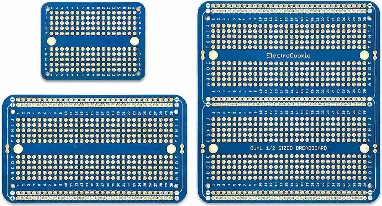
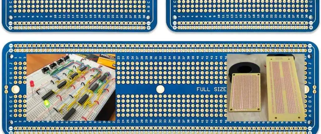
Stripboard, also known as Veroboard, is a versatile and popular prototyping medium for electronic circuits. This comprehensive guide will walk you through the intricacies of creating circuits on stripboard, from understanding its basic structure to mastering advanced techniques for reliable and efficient circuit design.
Understanding Stripboard Basics
What is Stripboard?
Stripboard is a type of prototyping board consisting of a rigid substrate with parallel copper tracks running in a single direction. Unlike breadboards, stripboard provides a more permanent solution for circuit development and testing. Its simple yet effective design makes it a favorite among hobbyists, students, and professional electronics engineers.
Q1: How do I prevent short circuits on stripboard?
A: Carefully cut tracks between components, use insulating tape if needed, and always double-check your track cuts with a multimeter before powering the circuit.
Q2: Can I reuse a stripboard after desoldering components?
A: Yes, but be cautious. Excessive heating can damage copper tracks. Clean the board thoroughly and inspect for any track damage before reuse.
Q3: What’s the difference between stripboard and breadboard?
A: Stripboard provides a more permanent solution with soldered connections, while breadboards offer temporary, solderless prototyping with easy component replacement.
Q4: How precise do track cuts need to be?
A: Cuts should completely separate the copper track. Use a magnifying glass or continuity tester to verify complete separation.
Q5: Are there alternatives to manual track cutting?
A: Some advanced users employ chemical etching or laser cutting for precise track modifications, but manual cutting remains the most accessible method.
Conclusion
Mastering stripboard circuit construction requires practice, patience, and attention to detail. By understanding the fundamentals, investing in proper tools, and developing precise techniques, you can create robust and reliable electronic circuits.
Whether you’re a hobbyist, student, or professional, stripboard remains an invaluable tool in the electronics prototyping arsenal. Continual learning and experimentation will enhance your skills and expand your capabilities in electronic circuit design.
Introduction: Why 5V Regulator Protection is Critical
5V voltage regulators power the backbone of modern electronics, from Arduino projects to industrial control systems. However, without proper protection circuits, these essential components remain vulnerable to electrical stress that can cause catastrophic system failures. This comprehensive guide explores how to design robust protection circuits that safeguard your 5V regulators and ensure long-term reliability.
Understanding 5V Voltage Regulators
What is a 5V Regulator?
A 5V voltage regulator maintains a constant 5-volt output regardless of input voltage fluctuations or varying load conditions. These regulators are indispensable for powering:
Integration with IoT connectivity for remote monitoring and control.
Adaptive Protection
Algorithms that adjust protection parameters based on operating conditions.
Self-Healing Circuits
Systems that automatically recover from fault conditions.
Conclusion
Implementing comprehensive protection circuits for 5V regulators is essential for creating reliable electronic systems. By understanding the various failure modes and protection techniques, engineers can design robust circuits that prevent damage and ensure long-term operation.
The key to successful protection design lies in:
Identifying all potential failure modes
Selecting appropriate protection methods
Proper component sizing and placement
Thorough testing and validation
Balancing cost with protection requirements
With careful attention to these factors, your 5V regulator protection circuits will provide years of reliable service, protecting valuable equipment and preventing costly downtime.
Additional Resources
For more detailed information on specific protection components and design techniques, consult manufacturer application notes and industry standards such as IEC 61000 for electromagnetic compatibility and IEC 60950 for safety requirements.
Programmable integrated circuits (ICs) like Field-Programmable Gate Arrays (FPGAs), Complex Programmable Logic Devices (CPLDs), and microcontrollers require precise identification through standardized markings. These markings are essential for proper identification, supply chain traceability, regulatory compliance, and preventing counterfeiting.
This comprehensive guide provides engineers and manufacturers with a structured approach to defining effective IC marking procedures that balance technical requirements, regulatory compliance, and operational efficiency.
What is Programmable IC Marking?
Programmable IC marking consists of alphanumeric codes, symbols, logos, and identifiers that are printed or laser-etched directly onto the IC surface. These markings serve multiple critical functions:
Product identification through unique part numbers and manufacturer details
Supply chain traceability for quality control and recall management
Regulatory compliance with international standards like RoHS, CE, and UL
Brand protection through manufacturer logos and anti-counterfeiting features
Programming status indicating whether the IC is blank or pre-programmed
Essential Elements of IC Markings
Core Information Requirements
Part Number: The unique model identifier (e.g., XC7A35T-1CPG236C for Xilinx FPGAs) that specifies the exact IC variant and capabilities.
Manufacturer Identity: Company name or logo for brand recognition and authenticity verification.
Date Code: Manufacturing date in standard format (e.g., 2125 for week 25 of 2021) enabling age tracking and warranty management.
Lot/Batch Code: Production batch identifier crucial for traceability and quality control investigations.
Country of Origin: Required for customs compliance and international trade regulations.
Additional Marking Elements
Regulatory Symbols: Compliance marks such as RoHS, CE, FCC, or AEC-Q100 for automotive applications.
Programming Information: Status indicators like “Blank,” “Pre-Programmed,” or firmware version numbers.
Security Features: Anti-counterfeiting elements including unique serial numbers, QR codes, or holographic elements.
Step-by-Step Marking Procedure
Phase 1: Requirements Analysis
Regulatory Research Begin by identifying all mandatory markings for your target markets. European markets require CE marking, while China mandates CCC marks for certain products. Environmental regulations like RoHS must be clearly indicated on compliant devices.
Industry Standard Compliance Follow established standards such as JEDEC JESD22-B111 for moisture sensitivity requirements and IPC-7351 for component labeling guidelines. Military and aerospace applications require adherence to MIL-STD-883 or AS9100 standards.
Phase 2: Content Definition
Mandatory Information Framework Establish the core elements that must appear on every IC: part number, manufacturer identification, manufacturing date, and country of origin. These elements form the foundation of your marking system.
Optional Enhancement Features Consider adding firmware version numbers, programming status indicators, or application-specific text like “For Industrial Use Only.” These additions provide valuable information for end-users and system integrators.
Security Integration Implement anti-counterfeiting measures through QR codes linked to authentication databases or laser-etched serial numbers that are difficult to replicate.
Phase 3: Layout Design
Spatial Optimization Design markings to fit within available IC surface area, typically 3×3 mm for compact packages. Avoid placement near wire bondingpads, thermal vias, or heat-sensitive regions that could affect IC performance.
Typography Selection Use clear, legible fonts such as sans-serif typefaces (Arial recommended) with minimum heights of 0.5 mm for laser etching and 1.0 mm for ink printing to ensure readability under magnification.
Visual Hierarchy Arrange information by importance, placing critical identifiers like part numbers in prominent positions while organizing secondary information logically around the primary markings.
Phase 4: Technology Selection
Laser Marking Systems Ideal for permanent, high-precision applications with excellent durability. Best suited for ceramic or plastic packages (QFP, BGA). While initial equipment costs are high, operating costs are low with no consumables required.
Inkjet Printing Cost-effective solution for high-volume production with lower equipment investment. Suitable for consumer electronics where absolute permanence isn’t critical. Consider environmental protection for outdoor or harsh-environment applications.
Chemical Etching Provides deep, tamper-proof markings primarily for metal-can packages. Offers excellent durability but is limited in package compatibility and design flexibility.
Phase 5: Quality Validation
Automated Inspection Implement Automated Optical Inspection (AOI) systems using machine vision to verify marking alignment, contrast ratios, and character legibility. Establish minimum contrast thresholds (typically 30% for laser marks).
Environmental Durability Testing Subject marked samples to accelerated aging tests including humidity exposure, temperature cycling (-40°C to 125°C), and UV radiation to verify marking permanence under operational conditions.
Human Readability Assessment Conduct systematic readability tests using standard magnification tools to ensure markings remain legible throughout the product lifecycle.
Phase 6: Traceability Implementation
Database Integration Develop centralized tracking systems linking lot codes and serial numbers to production records, enabling real-time supply chain visibility and rapid response to quality issues.
Digital Code Integration Implement 2D barcodes or QR codes encoding essential product information for rapid scanning and automated data capture throughout manufacturing and distribution processes.
Phase 7: Documentation and Training
Specification Documentation Create comprehensive marking specification documents detailing approved fonts, sizes, placement coordinates, contrast requirements, and inspection criteria. Include visual examples and tolerance specifications.
Personnel Training Conduct thorough training programs for production staff, quality inspectors, and suppliers to ensure consistent implementation and proper handling procedures.
Phase 8: Continuous Improvement
Regular Auditing Establish periodic review cycles to assess marking quality, compliance status, and effectiveness. Update procedures to reflect regulatory changes or design improvements.
Feedback Integration Collect input from field engineers, customers, and supply chain partners to identify improvement opportunities and address practical challenges.
Common Challenges and Solutions
Space Limitations
Challenge: Miniaturized packages like WLCSP provide minimal marking area. Solution: Develop standardized abbreviation systems and prioritize critical information. Consider alternative marking locations on package substrates.
Cost vs. Durability Trade-offs
Challenge: Balancing marking permanence with production economics. Solution: Apply risk-based marking strategies, using premium methods for high-reliability applications while optimizing costs for commercial products.
Counterfeiting Prevention
Challenge: Sophisticated counterfeiters can replicate standard markings. Solution: Implement multi-layer security including cryptographic QR codes, holographic elements, and database verification systems.
Industry Best Practices
Standardization Across Product Lines Maintain consistent formatting conventions for part numbers, date codes, and layout structures to reduce confusion and streamline manufacturing processes.
Critical Information Prioritization Position the most important identifiers (part numbers, lot codes) in the most visible and protected locations on the IC package.
Process Automation Leverage automated inspection systems to minimize human error, increase throughput, and maintain consistent quality standards.
Early Validation Test marking procedures during prototyping phases to identify and resolve issues before full production implementation.
Case Study: Automotive FPGA Marking
Project Requirements
An automotive supplier needed compliant markings for engine control unit FPGAs meeting AEC-Q100 automotive standards with enhanced durability for harsh operating environments.
Implementation Strategy
The team selected laser marking on ceramic packages, incorporating part numbers, date codes, AEC-Q100 compliance logos, and QR codes for complete traceability.
Validation Process
Extensive testing included thermal cycling (-40°C to 125°C), vibration testing, and salt spray exposure to verify marking durability under automotive operating conditions.
Results
The implementation achieved full regulatory compliance with durable, traceable markings that maintained legibility throughout accelerated life testing equivalent to 15 years of automotive operation.
Future Technology Trends
Smart Marking Systems
Emerging technologies include embedded RFID tags and NFC-enabled codes providing real-time tracking capabilities and enhanced authentication features.
AI-Enhanced Inspection
Machine learning algorithms are being developed to detect subtle counterfeiting attempts and automatically adjust inspection parameters for optimal quality control.
Sustainable Marking Solutions
Environmental considerations are driving development of eco-friendly marking inks, energy-efficient laser systems, and biodegradable security features.
Conclusion
Successfully defining programmable IC marking procedures requires systematic planning, cross-functional collaboration, and careful attention to regulatory requirements. By following structured implementation phases and incorporating industry best practices, manufacturers can develop marking systems that enhance product identification, ensure compliance, and protect against counterfeiting while optimizing production efficiency.
The continued evolution of programmable ICs demands ongoing adaptation of marking procedures to address new technologies, regulatory changes, and security challenges. Organizations that invest in robust marking systems will benefit from improved supply chain visibility, enhanced product authentication, and stronger customer confidence in their products.
Frequently Asked Questions (FAQs)
General Questions
Q: What is the difference between programmable and non-programmable IC marking? A: Programmable IC markings often include additional information such as programming status (blank or pre-programmed), firmware version numbers, and security features for field updates. Non-programmable ICs typically only require basic identification markings like part numbers and manufacturing details.
Q: How long do IC markings need to remain legible? A: Marking durability requirements vary by application. Consumer electronics typically require 5-10 years of legibility, while automotive and industrial applications may require 15-25 years. Military and aerospace applications often require markings to last the entire operational lifetime, which can exceed 30 years.
Q: Are there international standards for IC marking? A: Yes, key standards include JEDEC JESD22-B111 for moisture sensitivity markings, IPC-7351 for component labeling, and ISO/IEC 80079 for explosive atmosphere equipment. Regional requirements include CE marking for Europe and CCC marking for China.
Technical Questions
Q: What is the minimum font size for IC markings? A: Minimum font heights are typically 0.5 mm for laser etching and 1.0 mm for ink printing. However, this may vary based on package size, marking technology, and readability requirements. Some miniaturized packages may require smaller fonts with enhanced contrast.
Q: Can QR codes be used on small IC packages? A: Yes, QR codes can be miniaturized to fit on IC packages as small as 3×3 mm. High-resolution laser marking systems can create readable QR codes containing basic product information, though data capacity is limited by size constraints.
Q: How do you prevent thermal damage during laser marking? A: Use pulsed laser systems with controlled power settings, optimize marking speed to minimize heat buildup, and select appropriate wavelengths for the package material. Conduct thermal analysis during process development to establish safe operating parameters.
Compliance and Quality Questions
Q: What happens if IC markings don’t meet regulatory requirements? A: Non-compliant markings can result in customs delays, market access restrictions, product recalls, and regulatory penalties. In severe cases, products may be banned from certain markets until compliance is achieved.
Q: How often should marking quality be inspected? A: Implement statistical process control with sampling rates based on production volume and criticality. Typical inspection frequencies range from 100% for aerospace applications to statistical sampling (e.g., 1 in 100) for commercial products.
Q: What anti-counterfeiting measures are most effective for ICs? A: Multi-layer approaches work best, combining physical security features (laser-etched serial numbers), digital authentication (encrypted QR codes), and database verification systems. No single method is foolproof, but layered security significantly increases counterfeiting difficulty.
Production and Cost Questions
Q: What’s the cost difference between marking technologies? A: Laser marking has higher equipment costs ($50,000-$200,000) but lower per-unit costs and no consumables. Inkjet systems cost less initially ($10,000-$50,000) but require ongoing ink and maintenance expenses. Choose based on production volume and durability requirements.
Q: Can existing production lines be retrofitted with marking systems? A: Yes, most marking systems can be integrated into existing production lines. Consider factors like line speed, package handling requirements, and available space. Modular marking systems offer flexibility for retrofit applications.
Q: How do you handle marking for different package types in the same product family? A: Develop scalable marking templates that adapt to different package sizes while maintaining consistent information hierarchy. Use standardized abbreviations and symbols that work across all package variants to maintain brand consistency and reduce training requirements.
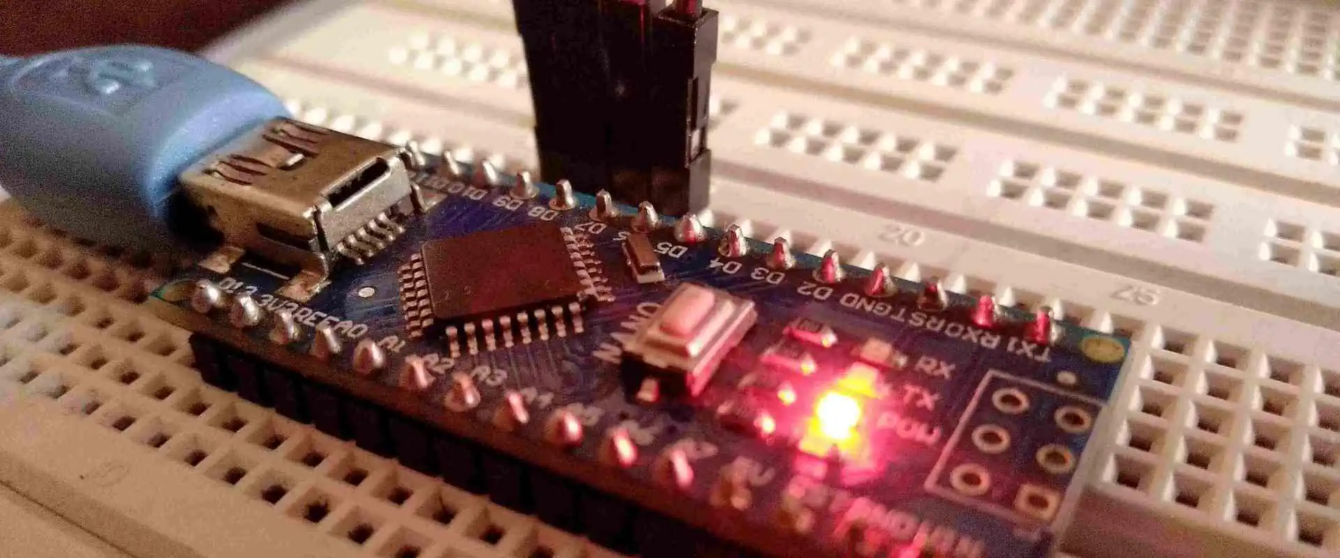
In this final installment of our microcontroller tutorial series, we will delve into the practical aspects of bringing your microcontroller-based project to life: soldering and programming the circuit. By this stage, you should have a solid understanding of microcontroller basics, circuit design, and component selection. Now, it’s time to assemble your circuit and program the microcontroller to perform its intended functions. This tutorial will guide you through the soldering process, programming techniques, and troubleshooting tips to ensure your project is successful.
1. Introduction to Soldering
Soldering is the process of joining two or more electronic components together using a filler metal called solder. It is a fundamental skill in electronics, enabling you to create permanent and reliable connections between components and a printed circuit board (PCB). Proper soldering ensures that your circuit functions as intended and minimizes the risk of loose connections or short circuits.
1.1 Tools and Materials Needed
Before you begin soldering, gather the following tools and materials:
Soldering Iron: A temperature-controlled soldering iron is ideal for precision work.
Solder: Use rosin-core solder with a diameter of 0.8mm or 1mm for general-purpose soldering.
Flux: Flux helps improve the flow of solder and ensures clean connections.
Soldering Stand: Keeps the soldering iron safe when not in use.
Sponge or Brass Wool: For cleaning the soldering iron tip.
Desoldering Pump or Braid: For correcting mistakes or removing components.
PCB and Components: Your designed circuit board and the necessary components.
Safety Gear: Safety glasses and a well-ventilated workspace.
Prepare the Soldering Iron: Heat the soldering iron to the appropriate temperature (typically 300-350°C). Clean the tip using a damp sponge or brass wool.
Position the Components: Insert the components into their designated holes on the PCB. Ensure they are flush against the board and properly aligned.
Apply Heat and Solder: Touch the soldering iron tip to the component lead and PCB pad simultaneously. After a second, feed a small amount of solder onto the joint. The solder should flow smoothly and form a shiny, cone-shaped joint.
Inspect the Joint: A good solder joint should be smooth, shiny, and free of cracks or voids. If the joint looks dull or lumpy, reheat it and add a bit more solder.
Trim Excess Leads: Use wire cutters to trim any excess component leads close to the solder joint.
1.3 Common Soldering Mistakes
Cold Joints: Occur when the solder doesn’t melt completely, resulting in a weak connection. Reheat the joint and add fresh solder.
Bridging: Happens when solder accidentally connects two adjacent pins or pads. Use desoldering braid to remove excess solder.
Overheating: Excessive heat can damage components or lift PCB pads. Work quickly and avoid prolonged contact with the soldering iron.
2. Assembling the Circuit
Once you’ve soldered all the components onto the PCB, it’s time to assemble the circuit. Follow these steps:
Double-Check Connections: Use a multimeter to verify continuity and ensure there are no short circuits or open connections.
Secure the PCB: Mount the PCB in its enclosure or on a stable surface to prevent movement during testing.
Connect Power: Attach the power supply to the circuit, ensuring the voltage matches the microcontroller’s requirements.
Test Basic Functionality: Before programming, verify that the circuit powers up without issues (e.g., no smoke or overheating).
3. Programming the Microcontroller
Programming is the process of uploading code to the microcontroller, enabling it to perform specific tasks. The exact steps depend on the microcontroller you’re using (e.g., Arduino, PIC, STM32), but the general process is similar.
3.1 Tools and Software
Development Board (Optional): Some microcontrollers, like the Arduino, can be programmed using a development board.
Programmer/Debugger: Devices like the AVR ISP, ST-Link, or PICkit are used to upload code to the microcontroller.
IDE (Integrated Development Environment): Software like Arduino IDE, MPLAB X, or STM32CubeIDE for writing and compiling code.
USB Cable: For connecting the microcontroller to your computer.
3.2 Writing the Code
Open the IDE: Launch the appropriate IDE for your microcontroller.
Create a New Project: Set up a new project and select the correct microcontroller model.
Write the Code: Use C, C++, or another supported language to write your program. Include necessary libraries and define pin configurations.
Compile the Code: Check for errors and compile the code into a binary file (hex file) that the microcontroller can execute.
3.3 Uploading the Code
Connect the Microcontroller: Use a programmer/debugger or USB cable to connect the microcontroller to your computer.
Select the Programmer: In the IDE, choose the correct programmer and communication port.
Upload the Code: Click the “Upload” button to transfer the compiled code to the microcontroller.
Verify the Upload: The IDE will display a success message if the upload is complete. If there’s an error, check the connections and settings.
3.4 Debugging and Testing
Serial Monitor: Use the serial monitor in the IDE to view debug messages and monitor the program’s behavior.
LED Indicators: Add LEDs to the circuit to visually confirm the program’s execution.
Multimeter and Oscilloscope: Measure voltages and signals to ensure the circuit is functioning as expected.
4. Troubleshooting Common Issues
Even with careful assembly and programming, issues can arise. Here are some common problems and their solutions:
Circuit Doesn’t Power On:
Check the power supply connections and voltage.
Verify that the polarity of components like capacitors and diodes is correct.
Code Doesn’t Upload:
Ensure the programmer is properly connected and recognized by the IDE.
Verify that the correct microcontroller model and communication settings are selected.
Unexpected Behavior:
Review the code for logical errors or incorrect pin assignments.
Check for loose connections or faulty components.
Overheating Components:
Disconnect power immediately and inspect for short circuits or incorrect component values.
5. Best Practices for Soldering and Programming
To ensure a successful project, follow these best practices:
Work in a Clean, Organized Space: Keep your workspace tidy to avoid losing components or making mistakes.
Use Quality Tools: Invest in a good soldering iron, solder, and other tools for reliable results.
Follow Datasheets: Refer to the datasheets for your microcontroller and components to ensure proper usage.
Test Incrementally: Test each part of the circuit as you build it to catch issues early.
Document Your Work: Keep a record of your circuit design, code, and any changes you make for future reference.
6. Expanding Your Project
Once your circuit is soldered and programmed, you can expand its functionality by:
Adding Sensors: Integrate sensors like temperature, motion, or light sensors to gather data.
Connecting to Displays: Use LCDs or OLEDs to display information.
Implementing Communication: Add modules for Wi-Fi, Bluetooth, or serial communication to enable remote control or data transfer.
Enhancing Power Management: Incorporate battery packs or solar panels for portable or off-grid applications.
7. Conclusion
Soldering and programming are the final steps in bringing your microcontroller project to life. By mastering these skills, you can create reliable, functional circuits that perform a wide range of tasks. Remember to take your time, follow best practices, and don’t be afraid to experiment and learn from mistakes. With practice, you’ll gain confidence and be able to tackle more complex projects in the future.
This concludes our five-part microcontroller tutorial series. We hope these guides have provided you with a solid foundation in microcontroller basics, circuit design, component selection, and practical implementation. Happy building!
In the rapidly evolving world of electronic design, efficient methods for generating schematic symbols are crucial. CSV (Comma-Separated Values) files offer a powerful and flexible approach to streamline the symbol creation process across various electronic design automation (EDA) platforms.
Q1: How Accurate Are CSV-Generated Schematic Symbols?
A1: Accuracy depends on input data quality and generation algorithm sophistication. Properly structured CSVs can produce symbols with 95-99% fidelity to original component specifications.
Q2: Can I Generate Symbols for Complex Integrated Circuits?
A2: Yes, but complex ICs require more detailed CSV structures and potentially more advanced generation algorithms to capture intricate pin configurations.
Q3: What Are the Most Common Challenges in Symbol Generation?
A3: Primary challenges include managing diverse pin configurations, maintaining consistent visual representation, and ensuring cross-platform compatibility.
Q4: How Do I Handle Variations in Component Specifications?
A4: Implement flexible parsing mechanisms, use template-based generation, and develop robust error-handling routines to manage specification variations.
Q5: Are There Open-Source Tools for Symbol Generation?
A5: Multiple open-source solutions exist, including Python-based libraries and specialized EDA community scripts that facilitate CSV-to-symbol conversion.
Conclusion
Creating schematic symbols from CSV files represents a sophisticated intersection of data management, programming expertise, and electronic design principles. By understanding and implementing the comprehensive strategies outlined in this guide, designers can revolutionize their symbol generation work
Precision is paramount in printed circuit board (PCB) design, and the ability to seamlessly convert between different measurement units is a critical skill for electronics engineers and designers. This comprehensive guide explores the intricacies of switching between millimeters (mm) and mils in PCB layout software.
Q1: Is There a Universal Conversion Standard Across All PCB Design Software?
A1: While conversion principles are consistent, specific implementation varies between software platforms. Always verify conversion accuracy within your specific design environment.
Q2: How Precise Are Automatic Unit Conversion Tools?
A2: Modern conversion tools offer high precision (99.9%), but manual verification is recommended for critical design parameters.
Q3: Can Unit Conversion Affect Signal Integrity?
A3: Theoretically minimal impact, but precise conversion is crucial to maintain exact dimensional relationships in high-frequency designs.
Q4: What Are the Most Common Conversion Errors?
A4: Typical errors include rounding mistakes, grid misalignment, and incomplete library updates during conversion process.
Q5: How Often Should I Verify Conversion Accuracy?
A5: Recommended verification after initial conversion, before final design submission, and whenever design rules or component libraries are updated.
Conclusion
Unit conversion in PCB layout represents a sophisticated process requiring technical precision, systematic approach, and comprehensive understanding of dimensional relationships. By mastering these techniques, designers can seamlessly navigate between measurement systems while maintaining design integrity and manufacturing compatibility.


