How Main PCB Impacts the Functionality of Electronic Devices

Shengyi S1000-2 PCB

Printed circuit boards are of great importance in the electronics world. Also, our everyday devices feature PCBs. Most people donโ€™t understand the technology behind the devices they use. Therefore, it is important to understand the basics of a PCB.

A main PCB is the core of an electronic. It plays a crucial role in the performance of electronic devices. Also, the main PCB is the circuit board in which electrical components are mounted on. In this article, we will explain more on main PCBs and what function it offers.

What is a Main PCB?

A main PCB is a flat board that provides mechanical support to electronic components. Also, this board uses conductive pads to accept the terminals of the component. A main PCB uses planes and traces to electrically connect the componentโ€™s terminals.

There are two major functions of the main PCB. The first is to attach electronic components in specific locations on the outer layers. Secondly, it offers electrical connections between the terminals of a component. Also, the main PCB serves as the platform in which electronic components are carefully installed.

The main PCB is the building block of most electronic devices. Also, this PCB can be single-sided, double-sided, or multilayer. The main PCB is a flat sheet of insulating material that features a copper foil layer laminated to the substrate. Also, this board holds electronic circuits together. The main PCB features electroplate copper conductors. These conductors go through holes known as vias.

Furthermore, a main PCB can feature multiple layers of copper. The board complexity depends on the number of layers and the interconnection between them. Multilayer main PCB offers better signal integrity and more routing options. However, this main PCB can be very costly to manufacture. Also, it is time consuming.

The two-layer PCB is very easy to manufacture. This is because it features copper on the two sides. However, multilayer boards join additional internal copper layers. The four layer main PCB features more routing options compared to the two layer board.

Components of a Main PCB

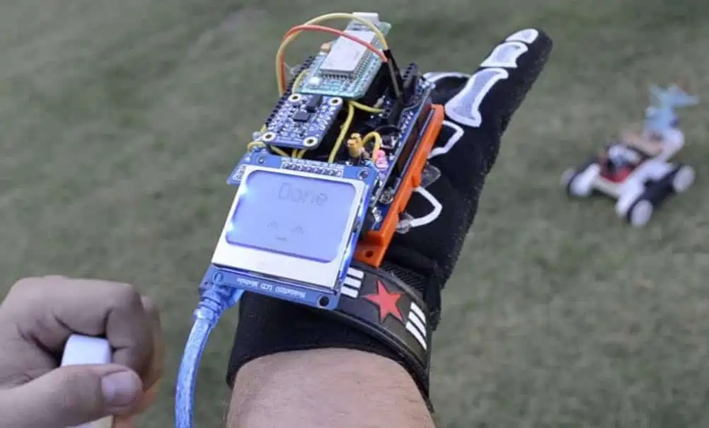
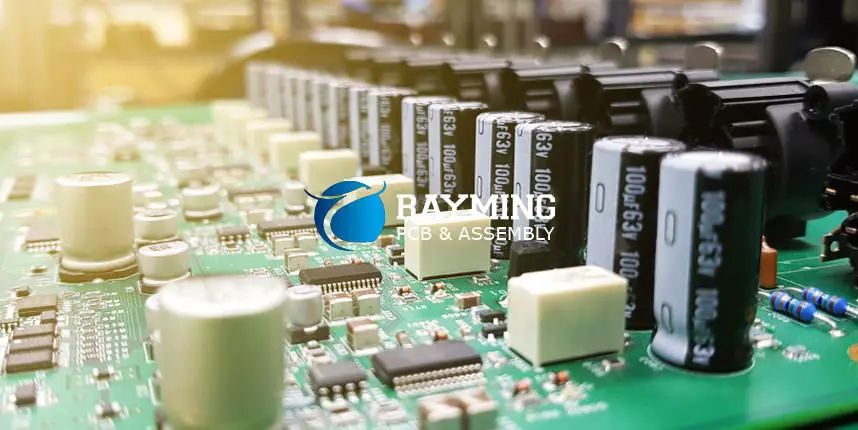
The main PCB features some electronic components. Also, these components are crucial to the performance of a device. The components of a main PCB include resistors, capacitors, and more. Each of the components on a main PCB has its own function. Some of the components on a main PCB include:

Capacitor

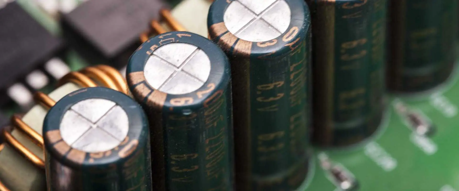
A capacitor holds electrical charge within the main PCB and discharges it. This component collects opposite charges on two different conductive layers.

Resistor

A resistor is a crucial component in the main PCB. This component enables the transmission of electric current. Therefore, it generates a voltage and discharges electric power as heat. Resistors are available in different materials. Also, these components are color coded to indicate their resistance value.

Sensor

The sensor plays a crucial role in a main PCB. This component indicates the changes in the environmental conditions. Therefore, it produces an electrical signal in response to the change it detected. This signal is then sent to other electronic components on the main PCB.

Diode

Diode is a component that enables the flow of electric current in one direction. Diodes can block the flow of current in the wrong direction. The light emitting diode (LED) is the most common diode.

Inductor

This is similar to a capacitor. An inductor stores energy in a magnetic field whenever current flows via them. Also, this component can block signals within the main PCB. It can block the interference from another piece of equipment.

Transistor

The transistor serves as an amplifier that controls electronic signals in a PCB. Also, there are various types of transistors. However, the bipolar transistor is the most common type. This transistor features the collector, emitter, and the base.

Materials Used for Main PCBs

The common materials used for the manufacturing of the main PCB include substrates, copper, and solder mask.

Substrates

The main PCB can feature flexible or rigid base materials. This depends on the PCB application. Also, rigid main PCBs use polyimide or FR4. However, flexible main PCBs utilize high-temperature polyimide films.  

Copper layer

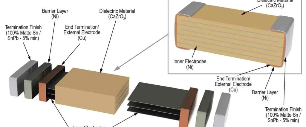
The copper layer is the copper coating or copper foil on one side or two sides of the PCB. The purpose of the copper layer is to offer electrical signals between the components on the board.

Solder mask

The soldermask is another primary material used for main PCBs. This material protects the PCB. Therefore it functions as a PCB skin. The solder mask is a protective material made of polymer.

Silkscreen

This material is also referred to as nomenclature. It is usually laminated on the component side of a main PCB. Also, the silkscreen layer helps to represent logos, settings, and symbol switches.

Main PCB Fabrication Process

The fabrication process of the main PCB involves several steps. The PCB manufacturer must carry out these steps carefully.

  • Develop the image of the circuit through photo tooling or direct imaging.
  • Remove too much copper from inner layers. This helps to reveal pads and traces.
  • Develop the PCB layer stackup by laminating PCB material with pressure and heat. Prepreg is necessary in this step as it facilitates the bonding process.
  • Drill holes to mount holes through vias and hole pins. The holes help to enhance the placement of components via PTH technology.
  • Apply a solder mask. Soldermask uses ultraviolet light. Also, apply the soldermask to the entire surface of the board for soldering metal pads.
  • Add surface finish to the board. There are various surface finish options for your PCB. Ensure you use the appropriate surface finish for your board.
  • Inspect and test the board for any defects or errors. This stage is critical as it ensures the functionality of your main PCB.

Conclusion

The main PCB is a core component of an electronic device. Without this PCB, an electronic device canโ€™t function. Therefore, this PCB is of great importance in electronics production. Also, the main PCB is widely used in different applications and industries. This PCB offers mechanical support and electrical connection to electronic devices.

What are the Functions and Characteristics of Amplifier PCB?

Amplifier PCB

Amplifier circuit boards play a crucial role in the designing of some electronic devices. These boards are often regarded as the heart of an amplifier. Amplifiers are useful in sound reproduction. Therefore, you will find amplifier PCBs in devices that generate sounds. For instance, a loud speaker features an amplifier PCB. Therefore, we will be discussing the amplifier circuit board in this article.

What is an Amplifier PCB?

An amplifier PCB is a circuit board that generates an enhanced version of an input signal that is fed into input terminals. This PCB is the building block of an amplifier. Typically, this type of PCB features some electronic components that accept a signal. Also, these components enhance the strength of an amplifier by passing the signal via a transistor or tube.  

PCBs are in different capabilities and sizes. However, they feature components soldered to a substrate. The most important part of the amplifier PCB is the substrate. The wafer on which the components sit is made of a resin reinforced with fiberglass.

Amplifier PCBs feature several electronic components. However, the actual amplifier is a single component. Furthermore, this board houses several capacitors and resistors that offer different functions. Also, it will feature output and input terminals for the amplified signal and original signal respectively.

Technically, many boards feature large heat sinks connected to the amplification component. An amplifier circuit board can be large or small. This depends on the application. Several portable headphone amplifiers are small. The circuit boards can measure a few square inches. However, amplifier PCBs for a professional audio or a large audiophile home amplifier can be very large. This PCB can measure more than 100 square inches.

Most times, amplifier PCBs lack one essential component which is the power supply. For a battery powered amplifier, the battery provides the power. Also, there is no need for intervening circuitry. Many small amplifiers integrate an external power supply. There are majorly two types of amplifier circuit boards. These are the audio and power amplifiers.

Difference between Amplifier PCBs and Normal PCBs

An amplifier PCB is different from a normal PCB. The manufacturing of a normal PCB requires the use of through-hole technology. This technology helps to mount PCB components and drill many holes. Also, another technology commonly used is the surface mount technology.

However, the manufacturing process of an amplifier PCB is different. This PCB is usually fabricated via a schematic capture. A software known as EasyEDA helps to place components. Also, the complexity of the circuit determines the physical aspects of the board.

Some factors are very important when placing components in an amplifier board. These are thermal and geometry factors. Also, in an amplifier PCB, the power output and input functions in response with the resistance of the transistors.

The dielectric constant of this PCB is better than that of a normal PCB. However, these two PCBs require the use of schematic diagrams in their design. Also, a normal PCB can be manually designed via a Photomask.

Functions of Heat Sinks in Amplifier PCBs

Amplifier PCBs feature heat sinks that help to dissipate heat generated during operation. Also, these heat sinks are usually made of aluminum materials. This is because these materials feature high conductivity levels. Also, the ability of aluminum to withstand abrasion and corrosion makes it a better option.

These heat sinks work with the help of thermovia and copper coins. Also, thermovia are holes located below heat-generating components. The heat sink is often mounted on the amplifier PCB. Also, the mounting of these sinks requires some components.

When mounting an amplifier PCB, components line solder pins and shur-lock tabs are essential.  Heat sinks play a crucial role in amplifier boards. These heat sinks enhance thermal management in amplifier PCBs.  Thermal management is crucial in amplifier boards.  

Uses of Amplifier PCB

Amplifier PCBs serve several purposes. These circuit boards are ideal for use in several applications. Also, these boards are the major point of operation when transforming analog signals to digital signals. First of all, the signals need to be amplified.

  • An amplifier PCB helps to enhance the amplitude of signals. While doing this, it maintains other aspects like frequency.
  • This PCB can transform analog signals to square waves. Therefore, it takes advantage of the high input saturation.
  • An amplifier circuit board has a high voltage and high output resistance. Therefore, this allows it to offer adequate output to drive loudspeakers.
  • This board helps to identify metal fatigue. Also, they help in ultrasound scanning and ultrasonic cleaning.
  • An amplifier board with a constant gain between AC and DC is useful in oscilloscopes.
  • There is not much gain due to the low input resistance of this board. Therefore, it functions as a buffer between the receiver and the circuitry. Also, it prevents unwanted signals.

Characteristics of an Amplifier PCB

Amplifier circuit boards possess the following characteristics:

High input impedance

This is very important at the input signal as it helps the voltage drop entirely on the amplifier. There will be no voltage drop across the amplifier for low input impedance. Therefore, amplifier circuit boards require low impedance materials. Also, high input impedance is crucial to avoid loading. The operational amplifier would absorb large amounts of current if it had low input impedance.

Limited bandwidth

It is crucial to consider a bandwidth that suits the frequency it should amplify when designing amplifiers. There will be loss of signal frequency if there is a narrow bandwidth. Meanwhile, there may be noise if the bandwidth is very wide.

High open-loop gain

This is the ability of an amplifier to enhance the power of the signal. This can be measured between the input and output ports when the circuit has no feedback. Also, it is very possible to get many feedback levels when there are high open loop gains.

Low output impedance

The signal amplifies when the voltage drops across the operational amplifier. You can lose signal across the device the amplifier feeds.

Conclusion

Amplifier PCBs have great uses and advantages. In this article, we have provided detailed information about amplifier circuit boards and what they do.

What is Microchip FPGA?

Microchip FPGA

Introduction to Microchip FPGAs

Microchip FPGAs are field programmable gate array chips designed and manufactured by Microchip Technology. As one of the leading FPGA vendors, Microchip offers a comprehensive portfolio of FPGAs for a wide range of applications.

This article provides an overview of Microchip’s FPGA products, key features and technologies, design software tools, target applications, and competitive positioning.

Microchip FPGA Product Families

Microchip has several FPGA product lines targeting different applications:

PolarFire FPGAs

PolarFire FPGAs are Microchip’s low power, security-minded FPGAs for demanding embedded applications.

Key attributes:

  • Lowest power consumption โ€“ up to 50% lower dynamic power
  • Defense-grade security features
  • Small form factors โ€“ from 100K to 500K logic elements
  • RISC-V CPU cores for hybrid FPGA+SoC designs
  • Radiation-tolerant options for space systems

SmartFusion2 SoC FPGAs

SmartFusion2 integrates an FPGA fabric along with an ARM Cortex-M3 CPU, memory, and peripherals for a complete system-on-chip (SoC).

Key highlights:

-166K to 500K FPGA logic elements

  • 800 MHz ARM Cortex-M3
  • Comprehensive I/O options including PCIe, Gigabit Ethernet and DDR3
  • Suitable for rugged embedded systems

IGLOO2 FPGAs

IGLOO2 chips are optimized as low power FPGAs for automotive, industrial and consumer applications.

Key features:

  • Very low static and dynamic power
  • Up to 150K logic elements
  • Cost-optimized design and fabrication
  • Extended temperature range options

RTG4 Radiation Tolerant FPGAs

The RTG4 FPGAs are designed for high reliability in space flight systems and high energy physics.

Highlights:

  • Exceptional radiation tolerance to single event effects
  • RTAX-S/SL rad-hard product grades
  • Up to 1.2M system logic cells
  • Wide temp range of -55C to +125C

This wide portfolio addresses needs across defense, automotive, industrial, aerospace, and other sectors.

Key Benefits of Microchip FPGAs

Microchip FPGAs offer several technology advantages compared to competitors:

Lowest Power Consumption

Through innovations like 40nm fabrication, advanced power gating, and voltage scaling, Microchip FPGAs achieve remarkably low static and dynamic power. This allows efficient deployment in power-constrained embedded systems.

Defense Grade Security Features

Microchip FPGAs provide hardware and intellectual property protection through secure boot, key management, authentication, anti-tamper detectors, and encryption engines.

RISC-V CPU Cores

Selected Microchip FPGAs feature RISC-V CPU cores for hybrid FPGA+SoC designs. RISC-V is an open standard instruction set architecture.

Radiation Hardness

For space applications, Microchip’s RTG4 and PolarFire FPGA options provide industry-leading radiation tolerance and reliability.

FPGA+SoC Convergence

Unique solutions like SmartFusion2 combine FPGA flexibility with ARM CPU capabilities for a pre-integrated SoC in one chip.

These technology capabilities allow Microchip to target a broad spectrum of embedded, industrial, aerospace and other applications.

Design Ecosystem

To simplify and accelerate development with Microchip FPGAs, the company offers several software tools:

Libero SOC Design Suite

Libero is Microchip’s unified IDE for FPGA design, simulation, synthesis, place and route, and programming. It streamlines the full FPGA workflow.

Key features:

  • Intuitive GUI with point and click design entry
  • Integration with popular HDLs such as VHDL and Verilog
  • ModelSim FPGA Edition simulator included
  • Timing driven place and route engine
  • Secure production programming capabilities
  • Support for all Microchip FPGA families

SoftConsole Integrated Development Environment

SoftConsole is an Eclipse based IDE for software development targeting Microchip’s SoC FPGAs like SmartFusion2 and PolarFire. It enables embedded C/C++ application development, RTOS integration, debugging and more.

MPLAB Harmony and MPLAB X

For ARM and PIC microcontroller development, Microchip provides the MPLAB ecosystem of tools including MPLAB Harmony SDK and MPLAB X IDE. These can be used in conjunction with SoC FPGAs.

By providing a unified set of design tools tailored for its FPGAs, Microchip simplifies and accelerates time to market.

Target Applications

Microchip FPGAs are designed into a diverse set of applications across industries:

Aerospace and Defense

  • Flight and weapons systems
  • Radar and imaging systems
  • Encryption and Secure communications

Automotive

Industrial

  • Motor drives
  • Power monitoring and control
  • Remote I/O modules

Medical

  • DNA sequencing instruments
  • MRI and imaging systems
  • Patient monitoring

Consumer

  • Hardware security modules
  • Home automation
  • IoT edge nodes

With their focus on low power and reliability, Microchip FPGAs are well suited for embedded systems in rugged environments. The company continues to expand into emerging applications like artificial intelligence (AI) as well.

Competitive Positioning

The FPGA market is dominated by Xilinx and Intel (formerly Altera). However, Microchip is staking out a strong position through its focus segments:

Low Power Embedded Systems

Microchip’s low power innovations have carved out a niche in embedded applications where Xilinx and Intel FPGAs are often too power hungry.

Radiation Hardened Aerospace

In the satellite and space segment, Microchip’s radiation tolerant RTG4 FPGAs have a commanding market share.

Automotive

FPGAs like IGLOO2 and PolarFire offer the reliability and security needed in vehicle systems.

Mid-Range Densities

By targeting FPGAs with 10K to 500K logic elements, Microchip avoids direct competition with the FPGA giants.

SoC Integration

Unique hybrid FPGA+SoC devices like SmartFusion2 provide integrated solutions unmatched by competitors.

Through these focused efforts, Microchip has emerged as a formidable contender in the global FPGA industry. The company is steadily gaining market share in many expanding applications.

Conclusion

In summary, key points about Microchip FPGAs:

  • Breadth of product portfolio covering different densities, markets, and features
  • Extensive design tool suite enables complete application development
  • Focus on low power, security, SoC integration and radiation hardness
  • Targeting key growth applications in defense, industrial, automotive, aerospace segments
  • Carving out specific niches vs leading vendors Xilinx and Intel

With each new product generation, Microchip continues innovating in power efficiency, performance, reliability, and security. Backed by its strengths in embedded systems, Microchip is cementing its position as a top FPGA provider for mission-critical applications.

Frequently Asked Questions

What are some of Microchip’s key FPGA product families?

Major FPGA families include PolarFire, IGLOO2, SmartFusion2, and RTG4. Each targets different densities, power levels, features, and applications.

What design software does Microchip offer for FPGA development?

Microchip provides the Libero SOC FPGA design suite, SoftConsole IDE for SoC development, and MPLAB ecosystem for programming and debugging.

What are some advantages of Microchip FPGAs over competitors?

Advantages include extremely low power, integrated SoC capabilities, radiation tolerance, defense-grade security, and a focus on the specific needs of embedded and industrial applications.

What applications are Microchip FPGAs designed for?

Key target applications span aerospace, automotive, industrial, medical, defense, and consumer segments. Specific uses cases include flight systems, vehicle networks, motor drives, patient monitoring and more.

How does Microchip position against the leading FPGA vendors?

Microchip carves out segments such as low power embedded, radiation hardening and SoC hybrids while avoiding head-on competition across the entire market with Xilinx and Intel.

What is the Difference Between ARM and FPGA Processors?

Xilinx Kintex-7 FPGA price

Introduction

ARM and FPGA are two very different types of processors used for a wide range of applications. Understanding the key differences between these architectures is important when selecting the right processor for a given application.

This article will provide an overview of ARM and FPGA processors, compare their architectures and performance attributes, analyze their programming approaches, and highlight suitable applications for each technology. Key differences will be summarized in tables throughout the article.

ARM Processors Overview

ARM processors are 32-bit and 64-bit RISC (Reduced Instruction Set Computer) CPUs that are designed for low cost and power efficiency. ARM cores are extremely popular in mobile and embedded devices due to their minimalist, power-optimized architecture.

Some key attributes of ARM processors:

  • RISC architecture with simpler instructions that execute in single clock cycles
  • Fixed hardware logic and execution pipelines
  • Excellent energy efficiency and low heat dissipation
  • Scalable performance from microcontrollers to application processors
  • Available as standardized cores licensed to many vendors
  • Requires software development in C/C++ or Assembly

ARM cores are used in billions of devices including smartphones, tablets, microcontrollers, and other embedded systems. Leading vendors like Qualcomm, Samsung, Nvidia, AMD, and Apple design their own ARM-based chips.

FPGA Processors Overview

FPGAs (Field Programmable Gate Arrays) are integrated circuits that can be programmed and reconfigured after manufacturing. This enables an FPGA to effectively morph into a custom computing device tailored for each application.

Key attributes of FPGAs:

  • Flexible fabric of logic blocks and routing that can be reconfigured
  • Parallel processing architecture optimized for data flow applications
  • Hardware level programmability using HDLs like Verilog or VHDL
  • High performance potential for parallel workloads
  • Well suited for DSP, ML, image processing, etc
  • Widely used for hardware acceleration and prototyping

While not as ubiquitous as ARM chips, FPGAs are popular for niche applications requiring custom hardware-level optimization and processing.

Architecture Comparison

ARM and FPGA processors have fundamental differences in their architecture and implementation:

ParameterARM ProcessorFPGA
Design PhilosophyRISC fixed architectureReconfigurable fabric
Processing ApproachSequential von NeumannParallel dataflow
Execution LogicFixed pipelines and data pathsReprogrammable logic blocks + routing
Hardware FlexibilityNone, fixed functionHighly flexible, customizable logic
Software FlexibilityHigh, can run different OS & appsLimited without HW changes
Performance AttributesPredictableApplication dependent
ProgrammingC/C++, AssemblyHDL (Verilog/VHDL)
Development ApproachSoftware algorithmsHardware logic synthesis

This table summarizes the key architectural differences between the two technologies:

RISC vs Reconfigurable Logic Architecture

The core design philosophy behind ARM and FPGA processors are completely different. The RISC architecture used in ARM chips has fixed hardware logic blocks tuned for efficiency in executing software instructions. In contrast, FPGAs contain a flexible fabric of logic blocks with programmable interconnects that can be rewired as needed.

Sequential vs Parallel Processing

ARM uses a classic sequential von Neumann architecture where instructions are executed one after another. FPGAs employ a dataflow architecture that processes data in parallel through customized pipelines. Multiple operations can occur simultaneously.

Fixed Pipelines vs Reconfigurable Logic

ARM processors rely on hardwired logic blocks and execution pipelines tailored for RISC instructions. With FPGAs, any hardware function can be synthesized using the basic logic elements, letting you customize data paths and control logic.

Software vs Hardware Flexibility

ARM processors are software-flexible – different operating systems and applications can run on the same ARM core. FPGAs are the opposite – they are hardware-flexible and must be physically reprogrammed for new functions, but software is largely fixed.

This contrast in fundamental architecture leads to major differences in performance, programming, and use cases.

Performance Comparison

Both ARM and FPGA offer excellent performance, but in very different ways:

Performance AttributeARM ProcessorFPGA
Processing StyleSequentialParallel
Clock SpeedsUp to ~3 GHzTypically 100-400 MHz
Latency10s – 100s of cyclesSingle cycle throughput
ThroughputGigabytes/secTerabytes/sec potential
Performance ScaleUp to multicore CPUs10X-100X speedups possible
Power EfficiencyExcellentConfigurable for efficiency
Cost EfficiencyLow cost per unitHigh development costs

Let’s analyze the key performance differences:

Sequential vs Parallel Execution

The von Neumann nature of ARM processors means they execute operations sequentially, albeit with some instruction parallelism via pipelines. FPGAs process data simultaneously in customized parallel pipelines, enabling much higher throughput. However, latency is lower on ARM cores.

Clock Speed Differences

ARM cores reach clock speeds up to around 3 GHz today by optimizing critical paths for fast sequential execution. FPGAs typically run at 100-400 MHz but make up for lower clocks through massive parallelism.

Throughput and Latency

ARM processors can complete single operations faster due to higher clocks (latency in 10s-100s of cycles). However, FPGA throughput for highly parallel tasks like encryption or image processing can be orders of magnitude higher (terabytes/sec).

Performance Scalability

ARM scales well to multicore CPUs with shared memory access. FPGAs can provide 10X-100X speedups for parallel workloads by customizing logic, but single thread performance lags.

Power and Cost Efficiency

ARM excels at power efficiency for mobile devices with clock gating and power management features. FPGAs can also be tuned for power efficiency but higher performance comes at a cost premium, while ARM chips leverage economies of scale.

For the right applications, FPGAs can significantly outperform ARM processors. But ARM remains superior for general purpose computing and single-threaded tasks.

Programming Model Comparison

ARM and FPGAs have completely different programming methodologies:

Programming AttributeARMFPGA
Primary LanguagesC/C++, AssemblyVerilog, VHDL (HDLs)
Abstraction LevelSoftware algorithmsHardware logic
Device LearningNot requiredMust learn FPGA fabric
Programming ApproachProcedural, sequentialConcurrent, parallel
DebuggingSoftware debuggingHardware verification
OptimizationCompiler optimizationsLogic synthesis optimization

Some key aspects:

Software vs Hardware Languages

ARM processors are programmed using software languages like C/C++ and Assembly to implement algorithms. FPGAs require hardware description languages (HDLs) like Verilog and VHDL that describe digital logic gates and connections.

Abstraction from Hardware

Software programmers can develop code without knowledge of the underlying processor. With FPGAs, you must understand the low-level fabric in order to synthesize logic that maps efficiently.

Programming Paradigm

ARM code is written procedurally with sequential instructions. FPGA logic must be designed concurrently with parallel data flows in mind. Different mental models are required.

Debugging and Optimization

Software debugging tools are more mature. FPGA optimization relies heavily on the synthesis tool mapping designs to the underlying hardware as efficiently as possible.

FPGA programming has a much steeper learning curve but enables hardware-level customization. ARM programming is more accessible thanks to abundant software resources.

Use Case Comparison

Given their differing attributes, ARM and FPGAs are suited for very different applications:

Use CasesARM ProcessorsFPGAs
Mobile devicesExcellent fitNot suitable
Embedded systemsWidely usedOverkill for most
IoT endpointsWell suitedPremium use cases
Cloud accelerationLimited suitabilityExcellent fit
DSP algorithmsCapable for many appsHigher performance possible
Computer visionOften sufficientMore demanding apps benefit
Autonomous vehiclesGenerally not usedCritical for some subsystems

Here are some typical use cases that favor ARM or FPGAs:

Mobile Devices

ARM processors are designed for mobile applications where low power draw is critical. FPGAs are overkill for smartphones and tablets due to cost and power constraints.

Embedded Systems

ARM MCUs and application processors power most embedded electronics like home appliances, sensors, industrial, etc. FPGAs are usually too expensive for mainstream embedded use.

IoT Endpoints

ARM Cortex M class MCUs feature in most IoT endpoint designs. Some higher performance IoT applications utilize FPGAs where ML acceleration is required locally.

Cloud Acceleration

FPGAs are widely used to accelerate computationally intensive tasks in data centers by customizing parallel pipelines. ARM servers have limited suitability currently.

Computer Vision

Lower resolution computer vision runs well on ARM chips. But FPGA acceleration becomes important for higher resolution or when deep learning algorithms are used.

Autonomous Vehicles

ARM processors typically do not have the performance for autonomous vehicle subsystems. FPGAs are critical for sensor fusion, perception, and decision making.

For any given application, the tradeoffs between these technologies must be carefully evaluated when selecting a processing platform.

Conclusion

ARM and FPGA processors have fundamental differences in architecture, programming, performance attributes, and typical applications.

Key Takeaways:

  • ARM processors feature a RISC architecture optimized for low cost and power efficiency. FPGAs provide a flexible fabric of logic blocks that can be reconfigured.
  • ARM uses a sequential von Neumann architecture while FPGAs leverage parallel dataflow processing.
  • FPGAs can accelerate suitable parallel workloads by 10X-100X but have a steep development curve. ARM offers broadly accessible software-based programming.
  • ARM excels in mobile and embedded devices. FPGAs are used where custom hardware acceleration is critical.

Understanding these complementary technologies is important when architecting systems. With their respective strengths, ARM and FPGAs will continue powering many of the world’s electronic devices into the foreseeable future.

Frequently Asked Questions

What are the key differences between ARM and FPGA architectures?

ARM uses fixed RISC processor cores while FPGAs provide reconfigurable logic fabrics. ARM has a sequential von Neumann architecture whereas FPGAs use a parallel dataflow architecture.

When is ARM processors the best choice over FPGA?

ARM processors are superior for mobile applications, embedded systems, and general purpose computing where low cost and power efficiency are critical. Their software programmability is also more accessible.

When is FPGA the right choice over ARM processors?

FPGAs are chosen for applications requiring custom hardware acceleration and parallel processing. They excel in cloud acceleration, high performance DSP and computer vision algorithms, and critical autonomy systems.

Can ARM processors be reconfigured like FPGAs?

No, ARM processors have fixed architecture and cannot be reconfigured at the hardware level. FPGAs can be reprogrammed even after manufacturing to morph into customized accelerators.

Do FPGAs completely replace ARM processors?

No, FPGAs complement rather than replace ARM processors in most systems. ARM CPUs are still used to execute control, I/O and application layer software alongside FPGA acceleration. The technologies have different strengths.

How Does a MEMS Motion Sensor Work ?

MEMS Motion Sensor

Introduction to MEMS Motion Sensors

A MEMS (Micro-Electro-Mechanical Systems) motion sensor is a tiny microchip that contains microscopic mechanical structures that can detect motion and acceleration. MEMS motion sensors have revolutionized the field of motion sensing and are used in countless applications today.

Some key facts about MEMS motion sensors:

  • They are extremely small, often just a few millimeters in size. This allows them to be integrated into tiny electronic devices.
  • They are inexpensive to manufacture in high volumes using semiconductor fabrication techniques. This makes them cost-effective options for motion sensing.
  • They can accurately measure motion, acceleration, vibration, tilt, and rotation along one, two, or three axes.
  • They have extremely low power consumption, making them suitable for battery-powered devices.
  • They can withstand high G-forces and harsh environments.

In this article, we will explore the underlying working principles and architecture of MEMS motion sensors. We will focus on two main types:

  • Accelerometers – measure linear acceleration.
  • Gyroscopes – measure angular velocity and orientation.

How Does an Accelerometer MEMS Motion Sensor Work?

An accelerometer is a MEMS sensor that measures proper acceleration or g-force. This is the acceleration experienced relative to freefall, which is caused by inertial forces. Accelerometers are essential components in devices where motion detection and tilt sensing are needed, such as smartphones, fitness trackers, game controllers, and drones.

The basic working principle of a MEMS accelerometer is that a small proof mass is suspended by springs inside a cavity. When the sensor experiences an acceleration, the proof mass deflects due to Newton’s second law of motion (F=ma). This deflection is then measured electrically to determine the acceleration.

Key Components

A MEMS accelerometer contains the following key components:

  • Proof mass – A tiny block of silicon attached to the substrate by suspension springs. It moves when accelerated.
  • Suspension springs – Hold the proof mass in place and allow it to deflect when accelerated. Made of silicon.
  • Capacitor plates – Stationary plates that measure capacitance changes as the proof mass moves between the plates.
  • Sensor substrate – A silicon wafer that forms the base. Etched using MEMS fabrication techniques.

Capacitive Sensing

The most common way accelerometers detect proof mass movement is by capacitive sensing. The principle is that the capacitance between two plates changes when the gap between them changes.

The proof mass forms one plate of a capacitor, while the substrate has fixed plates attached to it. As the proof mass moves due to acceleration, the gap between the plates changes, causing a change in capacitance. This change is converted to an electrical signal that is proportional to the acceleration.

By detecting capacitance changes along two or three axes, the accelerometer can measure acceleration in multiple dimensions.

Types of MEMS Accelerometers

There are several types of MEMS accelerometers based on their internal structure and sensing mechanism:

  • Piezoresistive – Uses piezoresistors on the spring arms to detect stresses.
  • Piezoelectric – Uses piezoelectric materials that produce a voltage when stressed.
  • Thermal – Contains heated gas in the cavity that changes temperature distribution when accelerated.
  • Tunneling – Uses quantum tunneling effects between tip and surface electrodes.

However, capacitive sensing is by far the most common approach due to its simplicity, low-power, and robustness.

How Does a Gyroscope MEMS Motion Sensor Work?

A gyroscope is a sensor that can measure angular velocity and orientation. MEMS gyroscopes are essential for inertial guidance systems, stabilizing cameras, VR headsets, drones and other applications where precise rotational motion sensing is needed.

While early gyroscopes contained spinning masses, MEMS gyroscopes work completely differently by using microscopic structures that leverage the Coriolis effect.

The Coriolis Effect

The Coriolis effect causes a deflection of moving objects when viewed in a rotating reference frame. On Earth, this effect causes moving air masses to be deflected, creating large-scale weather patterns and ocean currents.

In a MEMS gyroscope, the proof mass is driven to vibrate at a constant frequency by electrostatic forcing. When the sensor rotates, the vibrating proof mass gets deflected orthogonal to its original vibration axis due to the Coriolis effect. This deflection is measured capacitively to determine angular velocity.

By detecting deflections along multiple axes, the 3D rotational motion can be measured.

Types of MEMS Gyroscopes

There are two main types of MEMS gyroscopes:

  • Vibratory – Uses a vibrating proof mass as described above. Most common type.
  • Optical – Uses a resonating cavity and detects changes in light patterns when rotated. Complex but highly accurate.

Both types are able to measure angular velocity with a high degree of precision.

Fabrication of MEMS Motion Sensors

MEMS motion sensors leverage the same fabrication techniques used to manufacture integrated circuits and microprocessors. This enables mass production and integration with CMOS electronics. Here is an overview of the manufacturing process:

Silicon Wafer Preparation

Fabrication begins with blank silicon wafers about 1 mm thick. These wafers are highly polished on one side. An epitaxial layer is then grown on the polished side under vacuum and high heat. This layer defines the thickness and properties of the MEMS structures.

Depositing and Patterning Thin Films

Next, layers of conductive, insulating and piezoelectric materials are deposited on the wafer using techniques like chemical vapor deposition (CVD), sputtering, oxidation, and molecular beam epitaxy. Each material is patterned by photolithography and selective etching to form the electrodes, capacitor plates, and piezoelectric elements needed.

Bulk Micromachining

The silicon wafer is then etched from the backside to form cavities and tunnels where the MEMS structures will move. This bulk micromachining utilizes deep reactive-ion etching to carve extremely precise shapes out of the silicon.

Surface Micromachining

Additional layers are then deposited and patterned on the top surface to construct the delicate springs, weights, and gaps that make up the MEMS mechanical structures. The gaps are often sealed under vacuum or inert gas.

Capping and Dicing

In the final steps, the MEMS elements are sealed using wafer bonding under a protective cap. The wafer is then diced into hundreds of tiny MEMS motion sensor dies using a diamond saw. The dies are assembled into packages with electronics.

This entire process leverages the same equipment used to fabricate computer chips, allowing MEMS motion sensors to be manufactured in large volumes.

Applications of MEMS Motion Sensors

MEMS motion sensors are enabling many disruptive applications and technologies due to their microscopic size, low cost and excellent performance:

Consumer Electronics

  • Smartphones – Accelerometers for screen orientation and gyroscopes for pitch/roll/yaw sensing.
  • Game controllers – Accurate tilt and motion tracking for immersive gameplay.
  • Digital cameras – Image stabilization with gyroscope and accelerometer data.

Automotive Systems

  • Electronic stability control – Gyroscopes detect yaw and prevent skidding.
  • Airbag deployment – Accelerometers sense rapid deceleration for airbag release.
  • Navigation systems – Accelerometers augment GPS data for accurate position tracking.

Industrial

  • Condition monitoring – Vibration monitoring with accelerometers helps predict machine failures.
  • Platform stabilization – Gyroscopes and accelerometers enable stable positioning.
  • Robotics – Motion sensing for navigation, mapping and coordination.

Fitness and Sports

  • Wearable fitness trackers – Built-in accelerometers count steps and analyze workouts.
  • Smart footwear – Inserted sensors provide gait analysis and improve athlete performance.
  • Motion tracking – Accurately tracks complex motions like swings, pitches and more.

As MEMS fabrication continues to evolve, motion sensors will find new applications across industries. Their small size and low cost makes them ideal for integrating motion sensing capabilities into mass-market consumer products and niche industrial solutions alike.

Conclusion

MEMS motion sensors have completely transformed the fields of inertial guidance, motion tracking, and platform stabilization due to their microscopic size and excellent performance. By leveraging capacitive and Coriolis sensing principles, accelerometers and gyroscopes respectively provide precise measurements of linear and angular motion. With robust, cost-effective fabrication techniques adapted from the semiconductor industry, MEMS motion sensors will continue to enable innovative motion-aware devices and technologies.

Frequently Asked Questions

What are the key components inside a MEMS accelerometer?

MEMS accelerometers contain a movable proof mass suspended by springs, fixed capacitor plates to detect proof mass motion capacitively, and a substrate that houses these components. Acceleration deflects the proof mass and causes capacitance changes proportional to acceleration.

How does a MEMS gyroscope measure angular velocity?

It uses a vibrating proof mass. When the sensor rotates, the Coriolis effect causes the vibrating proof mass to deflect orthogonal to its vibration axis. This deflection is measured capacitively and is proportional to angular velocity.

What fabrication process is used to manufacture MEMS motion sensors?

Semiconductor micromachining techniques adapted from integrated circuit fabrication are used. This includes deposition, photolithography, bulk and surface micromachining, and wafer bonding/dicing to mass produce tiny MEMS structures on silicon wafers.

What are some applications of MEMS motion sensors?

Key applications are in consumer electronics like smartphones and game controllers, automotive systems like airbag deployment, industrial platforms and robotics, fitness wearables, and motion tracking in sports. Their small size and low cost make them widely usable.

What are the advantages of MEMS motion sensors over conventional motion sensors?

Compared to larger conventional sensors, MEMS motion sensors are microscopic in size, extremely low cost at high volumes, and have very low power consumption. Their performance is often superior despite the tiny footprint.

Functions of a PCB Controller in a Circuit Board

PCB controller

A circuit board electrically connects and mechanically aids the whole parts of an electronic device. Also, this board aids the proper functioning of an electronic device. A printed circuit board is often referred to as the heart of most electronics.

It is reasonable enough to design a PCB controller. A PCB controller can offer several functions. This PCB controller comes with generic specifications. For instance, a PCB controller can serve as a payment machine controller. This article seeks to provide more information about PCB controllers.

What is a PCB Controller?

A PCB controller plays a crucial role in the functioning of a circuit board. This component helps to perform different tasks. Also, a PCB is a chip designed for controlling electronic devices. A controller is stored in an integrated circuit. In addition, a PCB controller is often built on a PCB.

PCB controllers are widely used in consumer electronics and industrial applications. These controllers are widely used for several purposes. Also, a PCB controller designed for automotive applications can offer different specifications than one for wireless communication.

Generally, controllers are electro-mechanical devices which make use of input signals to change values. PCB controllers get voltage inputs from source and analyze these inputs. These controllers use via signal outputs to manage condition changes.

A PCB controller is usually mounted in control panels and enclosures. Also, this controller features inputs and outputs.

Factors to Consider When Choosing a PCB controller

When choosing a PCB controller, it is advisable to consider some factors. It is important to consider factors like speed and core size.  These factors depend on the applications of the PCB. For instance, core size impacts cost. Therefore, designers should choose as much as needed. Also, power and speed efficiency are trade-offs. Therefore, designers should consider the requirements of the intended application.

It is advisable to check out the peripherals that are active. This helps to optimize power consumption. Another important factor to consider is the control method. There are options for control methods. However, this varies by the type of PCB controller.

Also, designers need to consider the flash memory on the chip. It is important the chip has enough flash memory to backup applications.

How to Design PCB Controller

A general purpose PCB controllerโ€™s design requires generic specifications. Also, a PCB controller can perform different functions with several firmware. A general purpose PCB controller features a microchip and a microcontroller. Also, there are other components like power management and peripheral interface.

Switches and cables from external sensors run to the PCB controller. The controller is then well-secured to a terminal rack or industrial enclosure. It is ideal to design a general purpose controller on a single circuit board.

However, a cost saving design could need upgrade work when you consider the applications of these general purpose controllers. General purpose PCB controllers are widely useful in applications with exposure to harsh electrical environments. Therefore, it is advisable to use a modular design with several PCBs.

A general purpose PCB controller enables users to remove important components. You donโ€™t need to dismantle the entire unit from the enclosure. You can easily remove the faulty PCB module and plug a new one.

Best Design Practices for a General Purpose PCB Controller

To make upgrades and repairs easier, it is advisable to separate your controller into several modules. However, this may be a wasted effort if you donโ€™t segregate components well. The guidelines below will help you design a general purpose controller.

Separate the PCB controller into two modules. This is the MCU module and I/O module. Also, you will need to mount the I/O module into an enclosure. You can easily plug the MCU module into the I/O module. Passive PCB components with long life cycles are on the I/O module. The MCU module features more intelligent components like memory chips and the MCU.

Also, components like the memory chips and MCU can experience failure. Therefore, it is advisable to segregate high use and passive components. A component that is likely to fail should be on the easy-to-remove MCU module.  Also, there is a need for interconnectivity between the modules with board-to-board connectors.

In addition, it is important to allocate ground pins and sufficient voltage on the inter-board connectors. Designing PCB controllers requires carefulness. Therefore, it is important to consider ease of support and long-term brand reputation. Also, you have to focus on making firmware enhancements and excellent designs.

In addition, to achieve the best PCB controller design, a good software is crucial. The best PCB software helps you to design PCB controllers into modules. Also, this software can manage different schematic blocks.

Applications of PCB Controllers

PCB controllers are an important part of a PCB. This component plays a vital role. It is responsible for the proper functioning of a circuit board. Therefore, it is ideal for use in different applications.

Consumer electronics

Consumer electronics like smartphones and TVs feature PCB controllers. These electronics require a PCB controller to function properly. A wide variety of consumer electronics feature PCB controllers. Communication devices like smartwatches and tablets also feature PCB controllers.

Medical devices

Medical devices require PCB controllers to function well. PCB controllers are important for the functionality of these devices. For instance, devices like imaging systems and infusion pumps need PCB controllers. The medical industry has continued to use electronic devices.

Automotive components

Automotive components also feature PCB controllers. For instance, automotive components like navigation and sensors feature PCB controllers. Most systems that carry out some basic functions of a vehicle feature PCB controllers. Also, PCB controllers offer several functions in automotive components.

Industrial electronics

Electronics arenโ€™t only used for consumer purposes. Also, electronic appliances power several part of equipment in manufacturing and distribution centers. Appliances used in the industrial system require PCB controllers.

Conclusion

A PCB controller can offer several functions. This PCB controller is specifically designed with generic specifications. Also, it is a crucial component in a PCB. Therefore, it is ideal for use in several applications. We have discussed vital information about PCB controllers in this article.

Full tutorial capacitor symbol types and Capacitance formula

PCB Capacitor

Capacitors are one of the most commonly used passive components in electronics design. They store electric charge and find widespread use for applications like filtering, energy storage, timing circuits and more. Hundreds of capacitor symbols are used in circuit schematics to denote the various types and styles available.

This comprehensive tutorial provides a full reference on identifying capacitor symbols. We examine the symbols associated with different capacitor types based on dielectric material, structure, packaging and functionality. Useful tables summarize key details and a circuit example illustrates real-world usage. Finally, the standard capacitance formula is derived along with examples calculating capacitance for different geometries.

Capacitor Symbol Overview

Capacitor symbols represent two conductors or plates separated by an insulator or dielectric. Here are the most common generic symbols:

The parallel straight lines denote two separate conductors. When packaged, dashed lines may be added:

Polarity markers are sometimes used to denote the positive and negative terminals:

Fixed Value Capacitor Symbols

When the capacitor value is known, it can be specified numerically in units of Farads:

Standard metric prefixes like micro, nano or pico are used. Eg 10nF, 47ฮผF.

Variable Capacitor Symbols

Variable capacitors have symbols with arrows denoting tunability:

Trimmers are a type of variable capacitor tuned by a screwdriver for circuit calibration:

Polarized Capacitor Symbols

These indicate required polarity and terminal connections:

Electrolytic Capacitor Symbol

Often used in power supply filtering applications.

Tantalum Capacitor Symbol

Offers small size and reliability for surface mount boards.

Non-Polar Capacitor Symbols

These capacitors have no polarity requirements:

Ceramic Capacitor Symbol

Very common as cost effective SMD decoupling capacitors. Values up to few ฮผFs.

Mica Capacitor Symbol

Used for stable high tolerance capacitors. Expensive compared to ceramic.

Film Capacitor Symbols

Offer very high insulation resistance and low losses. Popular as coupling and by-pass capacitors.

Capacitor Symbols by Dielectric

Dielectric material also differentiates capacitor types:

Air Capacitor Symbol

Ideal dielectric but impractical size. Used for standards.

Vacuum Capacitor Symbol

Used when minimum dielectric loss is critical. Expensive to manufacture.

Glass Capacitor

Borosilicate glass as dielectric. Low loss, temperature-stable.

Mica Capacitor

Mica sheet between plates. Stable high Q capacitor.

Ceramic Capacitor

Made from porous ceramic materials. High volume SMD type. Values up to few ฮผFs.

Plastic Film Capacitor

Uses plastic films like polyester. Very high insulation resistance.

Electrolytic Capacitor

Uses electrolyte as dielectric to achieve high capacitance. Requires correct polarity.

Tantalum Capacitor

Uses tantalum pentoxide dielectric. Polarized, higher CV/volume ratio.

Capacitor Symbols Table Summary

SymbolCapacitor TypeCharacteristicsApplications
Fixed CapacitorKnown capacitance valueCoupling, decoupling, filters
Variable CapacitorTunable capacitanceTuning circuits, trimmers
ElectrolyticHigh capacitance, polarizedFiltering, energy storage
TantalumMedium capacitance, polarizedPortable electronics
CeramicLow cost, small sizesDecoupling, bypassing
FilmHigh stabilitySignal coupling, tuning
MicaStable, low lossHigh frequency tuning

Capacitor Symbols in Circuit Schematics

Here is an example circuit using multiple capacitor symbols:

  • C1 is fixed value AC coupling capacitor
  • C2 is variable trimmer capacitor
  • C3 is polarized tantalum capacitor
  • C4 and C5 are generic capacitors

This shows a real-world usage scenario of the various capacitor symbols in a schematic diagram.

Deriving Capacitance Formula

The capacitance value depends on physical and material aspects of the capacitor. Here we derive the basic parallel plate capacitance formula.

Consider two parallel plates of area A separated by distance d. When potential difference V is applied, charge Q gets stored:

Charge Q is proportional to voltage V:

Q = C * V

Where C is capacitance in Farads.

Capacitance C relates charge and voltage as:

C = Q/V

For parallel plates:

Q = ฮต * ฮต0 * A/d

Where:

  • ฮต0 is permittivity of free space
  • ฮตr is dielectric constant of material between plates

Therefore:

C = ฮต * ฮต0 * A/d

This is the capacitance formula for simple parallel plate capacitors.

More complex geometries like coaxial, cylindrical and spherical require modified formulas that incorporate their dimensions.

Example Capacitance Calculations

Let’s calculate the capacitance for some sample scenarios:

Parallel Plates

  • Plate Area A = 50cm x 50cm = 2500cm2
  • Separation d = 2mm = 0.02cm
  • Using air dielectric (ฮตr = 1)

Plugging in values:

C = ฮต0 * ฮตr * A/d C = 8.854 x 10-12 * 1 * 2500/0.02 C = 44.27nF

Cylindrical Capacitor

  • Inner radius r1 = 5mm = 0.05cm
  • Outer radius r2 = 10mm = 0.1cm
  • Length l = 20mm = 0.2cm
  • Using Teflon (ฮตr = 2.1)

Formula is:

C = (2ฯ€ฮตl)/ln(r2/r1)

Calculating:

C = (2*ฯ€*8.854x10-12*2.1*0.2)/ln(0.1/0.05) C = 24.2pF

Frequently Asked Questions

Multilayer Ceramic Capacitor

What does the capacitor symbol represent?

Capacitor symbols in schematics represent two conductors or plates separated by an insulator. This generic symbol is used for all capacitor types and styles.

How do you identify different types of capacitors?

Symbols may include polarity markers, value designations or specific styles to denote electrolytic, tantalum or variable capacitors. The circuit context also provides clues on likely type.

When should variable capacitor symbols be used?

Variable/tunable capacitors like trimmers have symbols with arrows on one or both plates. These are adjusted to set capacitance for tuning resonant circuits or calibration.

What is the most commonly used capacitor symbol?

The most ubiquitous capacitor symbol is the two straight parallel lines without polarity markers, representing fixed non-polarized capacitors. Common examples are ceramic disc capacitors.

What factors determine capacitance value?

Key factors affecting capacitance are plate area, separation distance between plates and the dielectric type. These geometric and material factors are incorporated in the standard capacitance formula.

What is Intel Agilex FPGA ?

Agilex FPGA

The Intel Agilex series marks the latest generation of FPGAs from Intel, succeeding the Stratix 10 lineup. First released in 2019, Agilex combines innovations in underlying FPGA fabric along with advanced SoC architecture to address the growing needs of data-centric applications.

This article provides a technical deep dive into the Agilex FPGA family. We examine the new HyperFlex architecture, embedded memory and DSP blocks, transceiver innovations, integrated PCIe 5.0, security features, device family variants and target applications for Agilex FPGAs.

Intel Agilex FPGA Overview

Here are some key highlights of the Agilex generation of Intel FPGAs:

  • Manufactured on 10nm process with 2nd generation HyperFlex architecture
  • Densities up to 1.7M logic elements (LE), 90Mb RAM and 48Mb FIFO
  • Up to 112G transceivers, PCIe Gen5 Hard IP blocks
  • Embedded controllers based on dual ARM Cortex-A53
  • Advanced security framework with cryptography accelerators
  • Support for HBM2/HBM2E memory integration
  • Designed for Data Center, Networking, Wireless Infrastructure and Military applications

HyperFlex FPGA Architecture

Agilex FPGA

Agilex FPGAs leverage an innovative fabric architecture called HyperFlex to deliver customized flexibility and performance.

HyperTiles

The basic building block of HyperFlex architecture is called a HyperTile. Each HyperTile contains:

  • Programmable Logic Blocks for implementation of logic
  • Local Hyper-Registers for sequential elements
  • Embedded Memory Blocks
  • DSP Slices for arithmetic operations
  • Interconnect for routing

By repeatable tiling of HyperTiles, different variants can be created within a single device family like Agilex.

Adaptive Fabric

A key capability of HyperFlex architecture is its adaptability to application requirements through the mix of HyperTile types, interconnect bandwidth and Precision DSP blocks.

This adaptability allows customization of an Agilex FPGA to optimize for bandwidth, logic utilization, signal processing needs or low power consumption.

Performance Benefits

HyperFlex enhancements yield significant gains over previous generation FPGAs:

  • Up to 40% higher logic density
  • Up to 2X increase in DSP performance
  • Up to 40% power savings

Combine to make Agilex suitable for high performance computing applications.

Agilex Device Family

The Agilex portfolio offers variants optimized for different application needs:

DeviceKey Features
Agilex FOptimized for lower cost and power
Agilex IHigh bandwidth I/O
Agilex MHigh DSP and memory density

Density options scale from 100K to 1.7M LEs. Higher density M models will be added in future.

Embedded Memory Blocks

On-chip memory resources available in Agilex FPGAs include:

M20K โ€“ 20 Kb embedded memory blocks, up to 3,522 blocks per device

MLAB – Smaller 640 bit registers, up to 1,966 per device

Provide 90Mb of embedded RAM along with advanced ECC support.

Integrated DSP Blocks

Agilex FPGAs integrate high performance DSP blocks called Hyper-DSP slices. Each slice contains:

-Multiply adder unit with 27×27 multiplier

-48-bit accumulator

-48-bit pre-adder

Deliver up to 7.4 TeraMACs of signal processing capability for wireless and image processing applications.

Programmable Analog

Analog mixed signal capabilities are enabled through:

FPAAs – Field Programmable Analog Arrays integrate programmable analog blocks

DSPs – Allow implementing data converters and PLLs

RTLs – Routable clock networks for synthesizing converters

PCI Express Hard IP

To support high speed interconnect, Agilex offers hardened PCIe Gen5 controller blocks with up to 32 lanes at 32GT/s data rates.

Delivers over 256GB/s bandwidth for 5G, networking and compute acceleration workloads.

Integrated HBM Memory Controllers

Large memory bandwidth is enabled by supporting integration of High Bandwidth Memory (HBM):

  • HBM2 – Up to 8-Hi stacks, 2.4Gbps per pin
  • HBM2E – Increased to 3.2Gbps per pin speed

Provides bandwidth up to 410GB/s from a single HBM2E stack.

Embedded ARM Controllers

Dual core ARM Cortex-A53 processors running up to 1.5 GHz are available as hard controller blocks. Used for managing and monitoring the FPGA fabric.

Security Framework

To safeguard applications, Agilex includes:

  • Hardware Root of Trust for secure device identity
  • DPA countermeasures and side channel analysis mitigation
  • AES-GCM 256-bit cryptography accelerators
  • Tamper resistant design with sensitivity analysis countermeasures
  • Support for securely downloading and updating FPGA images in the field

Transceiver Innovations

SerDes connectivity up to 112G PAM4 is enabled through enhancements like:

Multirate support – Ability to individually configure each lane’s rate from 6.4Gbps to 58Gbps

DSP Engine – Programmable DSP in each transceiver for defining equalization, sorting and interleaving

Embedded eye monitors – Monitor link health, eye diagrams without external equipment

Soft CDR – Digitally configurable clock data recovery allowing rate matching

Design and Programming

Agilex FPGAs are programmed using:

Intel Quartus Prime – Provides a unified environment for synthesis, place and route, timing analysis, power optimization and programming.

OpenCL – High level programming framework to accelerate applications in hardware.

Target Applications

Agilex families address a diverse set of workloads:

Data Center – Network acceleration, AI inferencing, big data analytics, storage

Wired Networking – 100G to 400G packet processing, network attached storage

Wireless 5G – Base stations, backhaul infrastructure, Remote Radio Heads (RRH)

Military/AvionicsRadar, communications, image processing

Test and Measurement – High speed automated test equipment (ATE)

Broadcast – Video bridging, compression, graphics

Frequently Asked Questions

What is the main innovation in Agilex architecture?

Agilex employs the new HyperFlex architecture which provides customizable FPGA fabric using tiles with adaptable interconnects, memory and DSP blocks. This architecture can be optimized across variants for specific application needs.

How does Agilex compare against earlier Intel FPGAs?

Agilex delivers higher performance, density and bandwidth compared to previous generation Stratix 10 FPGAs based on a 10nm manufacturing process and architectural enhancements.

What are the key application areas for Agilex FPGAs?

The primary segments for Agilex are Data Centers, Wired and Wireless Network Infrastructure, 5G, Military Embedded Systems, Test and Measurement Systems and Broadcast Video.

What is the main benefit of embedded controllers in Agilex?

The integrated ARM Cortex-A53 controllers allow managing the FPGA fabric, system bring up, communicating with host processors and implementing control logic without consuming programmable logic.

How does Agilex enable integration of HBM memory?

Agilex provides HBM2 and HBM2E memory controllers as hard IP blocks, enabling large external HBM stacks to be interfaced over high speed channels delivering up to 410GB/s bandwidth.

How to Choose the Best PCB Substrate for Board

materials for microwave PCB

Introduction

The printed circuit board (PCB) substrate, also known as the base material, serves as the foundation upon which the entire board is built. The properties of the substrate have a major influence on the performance, manufacturability and reliability of the PCB. With a wide variety of substrate materials available, from FR-4 to high-frequency laminates to ceramic and metal core boards, selecting the optimal material is critical.

This article provides a comprehensive guide on how to select the best PCB substrate material for a given application. It covers:

  • Overview of key PCB substrate materials
  • Important substrate properties and characteristics
  • Matching substrate properties to PCB requirements
  • Substrate recommendations for common PCB types
  • High frequency vs. low frequency substrate considerations
  • Factors driving substrate selection like cost, manufacturability etc.
  • Substrate properties comparison charts
  • Real-world examples of substrate selection

With the right knowledge, electrical engineers can choose a PCB substrate that maximizes performance, cost-effectiveness, manufacturability and reliability.

Overview of Major PCB Substrate Materials

Sheldahl Material

There are three broad classes of materials used as printed circuit board substrates:

Organic Substrates

Organic substrates, also known as laminates, use insulating polymer resins reinforced with fiberglass for mechanical strength. Some common types include:

  • FR-4 – Flame resistant glass-reinforced epoxy laminate. Most common low-cost substrate.
  • CEM-1 – Cotton paper and epoxy composite. Low cost option for low layer counts.
  • FR-5 – Woven glass reinforced epoxy with improved thermal performance over FR-4.
  • High-frequency laminates – PTFE or hydrocarbon based composites engineered for optimal RF/microwave performance. Rogers 4000ยฎ and 6000ยฎ series are common.
  • Flexible substrates – Polyimide films and laminates enabling flexible PCBs. DuPont Kaptonยฎ HN and Sheldahlยฎ flex materials widely used.

Inorganic Substrates

Inorganic substrate materials include ceramics and metal base boards:

  • Alumina – Aluminum oxide ceramic board. Provides excellent insulation and thermal properties.
  • Aluminum nitride – Higher thermal conductivity than alumina with similar electrical insulation.
  • Metal core boards – Base metals like aluminum or copper clad with dielectric for insulation. Highly thermally conductive.

Composite Substrates

Combine properties of organic and inorganic materials:

  • Metal-clad laminates – Organic FR-4 or polyimide laminate bonded to thin metal foil. Combines flexibility and shielding.
  • Ceramic-filled PTFE composites – Mix ceramic and PTFE to tailor dielectric properties and CTE. Rogers RO3000ยฎ series is a common type.

Now that we have outlined the major substrate material options, let’s look at how specific properties affect PCB performance.

Important Properties of PCB Substrate Materials

There are a number of key material properties that influence the choice of PCB substrate for a given application. Some of the most important ones include:

Dielectric Constant (Dk)

  • Defines how readily a material transmits electromagnetic waves.
  • Lower Dk allows faster electric signal propagation which improves high frequency performance.
  • Typical substrate Dk range: 2.5 to 10.8.

Dissipation Factor (Df)

  • Indicates how much signal loss occurs in a material.
  • Lower Df reduces losses and increases quality factor Q.
  • Typical substrate Df range: 0.002 to 0.025.

Coefficient of Thermal Expansion (CTE)

  • Indicates the degree to which a material expands with temperature.
  • Matching CTE between layers minimizes stresses and risk of delamination.
  • Typical substrate CTE range: 17 to 7 ppm/ยฐC.

Thermal Conductivity

  • Defines how readily heat transfers through a material.
  • Higher values enable better thermal management of heat-generating components.
  • Typical range: 0.25 to 170 W/m/K.

Glass Transition Temperature (Tg)

  • Indicates the temperature where a polymer transitions from rigid glassy state to soft rubbery state.
  • Higher Tg improves material stability at elevated temperatures.
  • Typical range: 130ยฐC to 280ยฐC.

Moisture Absorption

  • Moisture absorption lowers insulation resistance and can reduce reliability.
  • Lower values preferred for stable electrical performance.
  • Typical range: 0.1 to 5.0%.

Z-axis CTE

  • Indicates expansivity perpendicular to the board layers.
  • Lower Z-axis CTE minimizes interconnect stresses and via failures.
  • Typical range: 30 to 70 ppm/ยฐC.

Let’s look at how we match these substrate properties to the requirements of different types of PCBs.

Matching PCB Substrate Properties to Board Requirements

rogers substrate

To select the optimal PCB substrate material, you need to consider the electrical, thermal, mechanical and physical requirements of the specific application and match candidate materials accordingly.

Here is an overview of how substrate properties align with the needs of some common PCB types:

High Frequency RF/Microwave PCBs

  • Critical needs – Low Dk, low Df, stable electrical properties, controlled impedance
  • Candidate materials – PTFE or ceramic-filled PTFE laminates like Rogers RO3003; Hydrocarbon laminates like Rogers RO4350

High Layer Count Multilayer Boards

  • Critical needs – Dimensional stability, low Z-axis CTE, low moisture absorption, high Tg
  • Candidate materials – FR-4, high Tg epoxy laminates, PTFE composites

High Power PCBs

  • Critical needs – Thermal conductivity, dielectric strength, Tg, CTE match
  • Candidate materials – Insulated metal substrate, ceramic-filled laminates, ceramic boards

High Reliability Aerospace & Defense

  • Critical needs – Stable electricals, low moisture absorption, high flexibility
  • Candidate materials – Polyimide films, quartz-reinforced laminates

Automotive Electronics

  • Critical needs – Lead-free compatibility, thermal stability, flame resistance, robustness
  • Candidate materials – FR-4, high Tg laminates with UL 94 V-0 rating

Flexible Circuits

  • Critical needs – Flexibility, bend radius, chemical resistance, layer bond strength
  • Candidate materials – Polyimide films, reinforced flexible laminates

Let’s look at some specific recommendations for common PCB applications.

PCB Substrate Selection Guidelines

Here are some general guidelines on selecting the optimal PCB substrate material for different classes of boards:

Low Frequency/Digital PCBs

  • FR-4 – The baseline cost-effective choice. Serves most digital/low freq needs.
  • CEM-1 – Very low cost option for simple double sided boards without plated through holes.
  • FR-5 – Improves thermal conductivity over FR-4 while retaining UL rating.

RF and Microwave PCBs

  • PTFE laminates – Prime choice for >10 GHz. Low Dk and Df. Examples: Rogers RO3003.
  • Hydrocarbon laminates – Cost-effective option for moderate RF requirements. Rogers RO4350.
  • Ceramic filled PTFE -Tunable electrical properties. Rogers RO3006.
  • Quartz glass laminates – Extremely low loss for high freq. Rogers RT/duroid 6006.

High-Speed Digital PCBs

  • FR-4 – Primary choice. Serves most digital applications up to GHz range.
  • Halogen-free laminates – For environmental compliance requirements. Tachyon 100G.
  • Low-loss laminates – Help maximize signal integrity at multi-GHz frequencies. Rogers RO4350.

High Layer Count and HDI Boards

  • FR-4 – Widely used for high layer count boards up to 20+ layers.
  • High Tg epoxies – Enables lead-free assembly temperatures. Panasonic Megtron 6.
  • Low Dk laminates – Minimizes layer-to-layer crosstalk.

High Power and Thermal Management

  • Insulated Metal Substrate (IMS) – Metal core PCBs with dielectric coating. Highly thermally conductive.
  • Ceramics – High thermal conductivity and temperature resistance. Aluminum nitride or alumina boards.
  • Thermally conductive laminates – Enhanced dielectric thermal conductivity. T-lam and metal-clad laminates.

Flexible Circuits

  • Polyimide films – Prime choice. Kaptonยฎ or Upilexยฎ films enable high flexibility and bend radius.
  • Flexible laminates – Reinforced films for better dimensional stability. Dupont Pyraluxยฎ AP.

Automotive Electronics

  • FR-4 – Widely used thanks to proven reliability, UL rating and lead-free process compatibility.
  • High Tg laminates – Withstand higher temperatures. Panasonic Megtron DZ-2.
  • Halogen-free laminates – Meet environmental regulations. Isola 370HR.

This provides a good starting point for selecting substrates based on the PCB application. But there are many other factors driving material selection as we will see.

High Frequency vs. Low Frequency Substrate Considerations

Alumina Substrate
Alumina Substrate

Let’s compare some of the key considerations when choosing substrates for high frequency versus low frequency PCBs:

High Frequency RF/Microwave Substrates

  • Minimize dielectric constant and loss
  • Stable electrical properties over frequency and temperature
  • Controlled dielectric thickness and tolerance
  • Smooth copper surface
  • Thermal expansion matching between layers
  • Moderate glass transition temperatures

Low Frequency/Digital Substrates

  • Moderate dielectric constants acceptable
  • Loss and impedance control less critical
  • Focus on cost, manufacturability and reliability
  • Lead-free assembly compatibility
  • UL flammability ratings
  • Higher glass transition temperatures

While FR-4 is suitable for many digital boards, critical RF boards may require advanced low-loss laminates to achieve peak performance. But cost and manufacturability remain important considerations for any substrate type.

Key Factors Driving PCB Substrate Selection

Some of the main considerations when choosing a PCB substrate material include:

Electrical Performance

  • Dielectric constant, loss, breakdown voltage, leakage current
  • Impedance control, signal speed, signal integrity
  • Frequency range, power handling, Q factor

Thermal Performance

  • Thermal conductivity, maximum operating temperature
  • Thermal management of components and traces
  • Temperature cycling resistance, thermal shock performance

Mechanical Properties

  • Flexural and tensile strength, impact resistance
  • Hardness, chemical resistance, abrasion resistance

Physical Attributes

  • Flammability and fire resistance rating
  • CTE and mechanical stability
  • Moisture absorption, outgassing properties -Thickness and dimensional tolerance

Manufacturing Factors

  • Board fabrication process compatibility
  • Soldering and assembly process compatibility
  • Availability, lead times and cost
  • Ease of prototyping and fabricating high volumes

Reliability

  • Shock, vibration and acceleration tolerance
  • Withstand operating environment conditions
  • Lifetime performance under thermal cycling
  • Resistance to common failure modes

Understanding these multiple factors helps guide the substrate selection to match design requirements.

PCB Substrate Materials Properties Comparison

To help compare options, here is a table showing key property ranges for some common PCB substrate material types:

MaterialDkDfCTE (ppm/ยฐC)Thermal Cond. (W/m/K)Tg (ยฐC)
FR-44.2-4.80.02-0.02512-200.3130-140
CEM-14-50.02-0.0470-1400.23105-125
Rogers RO300330.0013170.31280
Rogers RO4350B3.480.003720-300.61>280
Taconic TLY2.90.00861.1280
Megtron 63.8-4.00.018-0.02512-150.35170
Alumina Ceramic9.40.0001724N/A
Aluminum Nitride8.80.00034.6170N/A
Polyimide3.40.008200.12260

This highlights how properties can vary widely between substrate families. The optimal balance depends on the priorities like cost, performance and manufacturability.

Real-World PCB Substrate Material Selection Examples

To help illustrate substrate selection in practice, here are some examples:

Case 1: Cell Phone RF Front End PCB

Requirements: Handle 5G FR2 frequencies up to 6 GHz, power amplification circuits, impedance control, low cost

Selected Substrate: Rogers RO4835, thin cores, LoPro prepreg

Case 2: Space Satellite Communications PCB

Requirements: Extreme stability over temp. cycling, non-outgassing, withstand vibration/shock, moderate freq. range

Selected Substrate: Polyimide laminate with quartz reinforcement

Case 3: High Power LED Lighting PCB

Requirements: High thermal conductivity to manage power dissipation, electrical insulation, metal trace patterns

Selected Substrate: Thermally conductive aluminum metal core substrate

Case 4: Automotive ABS Control Unit

Requirements: Lead-free soldering compatibility, flame resistance rating, withstand under-hood temperatures

Selected Substrate: FR-4 with high Tg resin system (>170ยฐC)

This illustrates how substrate selection depends on balancing the key electrical, mechanical, thermal, physical and manufacturing requirements of each unique PCB application.

Frequently Asked Questions about PCB Substrates

Here are some common FAQs related to selecting PCB substrate materials:

Q: What are some of the newest PCB substrate materials available?

Some newer materials include ultra-low loss laminates like Rogers RO3003 LoPro, thermally conductive substrates like Ventec VT-5A series, and LCP (liquid crystal polymer) films for flex circuits.

Q: How are substrate requirements different for double sided vs multilayer PCBs?

Multilayer PCBs demand tighter control of Dk and Df for impedance control, lower Z-axis CTE to minimize interlayer stress, and dimensional stability for thinner dielectrics.

Q: What materials enable embedded passives and components?

High frequency laminates compatible with laser drilling/ablation are preferred for embedded components. Thermally conductive materials aid heat dissipation.

Q: What substrate materials are suitable for rigid-flex PCBs?

Flexible polyimide films bonded to glass-reinforced laminates like FR-4 provide a solid rigid-flex solution. Adhesives and bondplys are used.

Q: How do material costs compare between standard and advanced substrates?

Standard FR-4 is lowest cost. Prices rise moving to high freq laminates, thermally conductive boards, and advanced ceramics.

Conclusion

Selecting the optimal PCB substrate material requires striking the right balance between electrical, thermal, mechanical and manufacturing properties to meet the needs of the particular application. While standard FR-4 will suffice for many digital and low frequency boards, engineers must take a broader perspective and consider advanced materials for more demanding applications.

The PCB substrate directly impacts many aspects of board performance, manufacturability, reliability and cost. Investing time upfront to make the best material choice based on design requirements will maximize the probability of success, avoid unnecessary risk, and prevent costly redesigns.

What Does it Mean to Breakout a BGA 0.4 MM Pitch?

BGA 0.4 MM Pitch

Having a pitch of 0.5mm and more, generally, we recommend that you use non-solder mask define pads for your ball grid arrays. This pad will ensure better adhesion as regards the ability of the solder to hold the copper sides as well as the topmost surface. With respect to BGA 0.5 mm pitch, majority of part manufacturers still prefer to use NSMD pass.

If granted, there is a need to ensure that the fab house has the ability to perform well when it has to do with mask registration. Thereโ€™s nothing good about having pads which are part (half) NSMD and part (half) SMD. Of course, we have seen that.

As soon as you reach the BGA 0.4 mm pitch, things will likely get different. Of course, we have started seeing more of these happening. In some wafer scale package (WSP) or chip scale package (CSL), LGA and BGA parts have started showing up in the BGA 0.4 mm pitch, and some larger parts such as the OMAP processor

Furthermore, at this size, youโ€™ll start seeing more risks associated with solder bridging with respect to NSMD pads. With small geometries, routing the escape traces on the topmost layer will not be possible as well. The pad has to be a solid metal with no exceptions. Avoid making use of a solder mask in capping the vias present at this pitch too. Make sure it is all metal.

Breaking out a BGA 0.4 mm Pitch

One thing all designers of printed circuit boards will agree on is that breaking out a BGA requires discipline and precision. When breaking out a ball grid array, you are applying a fanout solution. Then you will route the traces from the fanouts to the deviceโ€™s perimeter before the PCBโ€™s general routing. Below are two illustrations on a BGA 0.4 mm pitch breakout.

BGA 0.4 mm Pitch Breakout

To become a printed circuit board master for HDI begins with gaining knowledge on the breaking out of a BGA. Note that ball grid arrays (BGAs) are known to possess the largest density of array pins and I/O connections on a specific device. Regarding the layout, this part is very complex.

Since breaking out a BGA can be done in many ways, we will be teaching you with an example the process involved in breaking out a BGA 0.4 mm pitch. To ensure a great design practice, thereโ€™s a need to handle the layout systematically. You have to ensure that you can fanout, as well as connect the pads with the BGA. Drawing of short tracks is another great design practice.

Before you go ahead with breaking out a BGA 0.4 mm pitch, you have to consider the overall size as well as the pin out of that part. This way it becomes possible to make use of a technology that is very cost efficient.

To fan out a BGA 0.4 mm pitch, this geometry doesnโ€™t work out to help you route traces in-between the pins. Furthermore, the gaps and traces are usually very small to reach enough layers and then get the pins all fanned out.

Therefore, for a BGA 0.4 mm pitch, you will need a buried and blind vias. The routing of the pins present on the BGAโ€™s outermost row will be on Layer 1, while those on the following row will be on Layer 2. The way in which the BGA pins out determines the routing of the BGA.

Example 1: Breaking out a BGA 0.4 mm Pitch

This is a standard BGA 0.4 mm pitch. The most appropriate way of fanning it is making use of a blind and buried vias. You begin by adding the layer 1 to the layer 2 blind via on the entire BGAโ€™s GND pins. Now you have completed the job with the GND pins, and so there is no need to do the routing.

Drill and Pad Sizes for BGA 0.4 mm Pitch

Traces will be absent between the top layer pads. So, these pads could be 10 mils and then feature between them a 5.7 gap. Concerning the larger pads, allow the manufacturer to drill a laser drill of 4 to 5 mil for the blind and buried vias.

Also, the distance in-between the layers of the board have a huge role to play in the drill size. This will make it possible to shut the hole and then produce a flat pad to work with the BGA.

 Sequential Lamination

Now, letโ€™s say this board has 8 layers. You will laminate the second to the seventh layer together. From layer 2 to layer 3, you can make use of laser drill. Note that this will be your two to three 3 buried via. Also, take note that it is possible to use a buried via of layer seven to six. This also holds for layer two to layer 7. However, thereโ€™s a need for the two to seven to have a larger pad and drill.

The first and eighth board layers will now undergo lamination on the board. Also, you will conduct a laser drill from the first layer to the second layer. If needed, you can also do the tenth to the ninth layer.

Example 2: Breaking out a BGA 0.4 mm Pitch

Here, we are dealing with a BGA 0.4 mm Pitch on a 6 by 6 matrix. Its space/trace is 4 to 5 mil, with 8-mil pads and 4-mil lasers. Furthermore, the routing strategy features staggered and stacked vias.

Also, the PCB features 4-mil vias. Furthermore, the thickness of the material between the first and second layers has to be a maximum of 4 mils. The rule for the aspect ratio requires a dielectric of 4 mils between the first and second layers. Also, you must keep the stackups symmetrical.

Conclusion

We hope we have explained to you how to breakout a BGA 0.4 mm pitch. To have a full understanding, we advise that you read it over again. Please feel free to ask you questions if you have any.