TPS54308DDCR is a Buck Converter IC with Component Reduction Capabilities

TPS54308DDCR

A buck converter, also called a buck regulator, is a regulator device added to a circuit board as an Integrated Circuit (IC). It is a one of the types of DC-to-DC converters and like the converters, the regulator helps to โ€œbalanceโ€ or โ€œeven outโ€ the current.

There are several variations of this out there and Texas Instruments is one of the leading manufacturers. The company has manufactured a standalone buck converter but this time, it made the TPS54308DDCR into a buck regulator with synchronization features.

If you are looking for an all-around buck regulator that does a combo of power or current regulation and component reduction; you have one here on the TPS54308DDCR.

So, in this article, we are going to talk extensively about how it works.

The Synchronous Operations

TPS54308DDCR is a 28-V, 3-A, synchronous buck converter IC, meaning that it offers multiple functions at once. For emphasis, it supports the following:

  • The implementation of a constant-frequency, peak current mode control. This control features helps to reduce the systemโ€™s output capacitance.
  • It improves the systemโ€™s performance both during the load and line transients.
  • TPS54308DDCR leverages the optimized internal compensation network to simplify the control loop design and to improve the minimized use of external components.

Advanced Current Protection

FULL PCB MANUFACTURING Quote

There is no doubt that one of the functions of a buck regulator is to simplify the current conversion process. However, TPS54308DDCR implements an advanced form in the form of a cycle-by-cycle current limit.

It is a current-limiting feature implemented on both the high-side MOSFETs. The implementation goes a long way to bolster the TPS54308DDCR systemโ€™s protection, when it is operating in an overload or overvoltage mode.

Another part of the current protection is the implementation of the low-side MOSFET freewheeling current limit. It is a โ€œcurrent enhancing featureโ€ that prevents current runaway in TPS54308DDCR.

Just like the above protective features are improving TPS54308DDCRโ€™s current protection, there is also another feature that does it better. The name is Hiccup Mode Protection. It comes in handy when the system has been in an overcurrent or overvoltage current for a long time. When that happens, the Hiccup Mode Protection would be triggered to further protect the system after the overcurrent condition persists.

TPS54308DDCR Reduces Component Counts

More components added to the buck converter could further the expansion and depending on the application, it might not be worthwhile. Therefore, it is pertinent to have measures in place to reduce the proliferation of additional components added into the system.

TPS54308DDCR uses the combination of internal loop compensation, two (3) integrated switching FETs and a 5-ms internal soft start function to reduce the number of components used.

Like Limited Components; Like Smaller Footprints

Just like the TPS54308DDCR reduces component counts, it is also doing that to maintain the smaller footprint design.

By default, the system integrates MOSFETs and use a small-sized SOT-23 package/case. The combo allows for the system to integrated and used with many applications requiring a smaller footprint. Besides, these features also enable the system to achieve a higher power density.

Current Inrush Minimization

It is also possible to minimize or reduce the speed at which current flows into the IC. That is done through TPS54308DDCRโ€™s support for the 5-ms soft-start time function. It helps to regulate the speed of current flowing into the system.

TPS54308DDCR Uses an Overvoltage Comparator

Sometimes, the reason why a circuit board or an electronic device has more voltage than it can handle is because there is no โ€œregulatory deviceโ€ in place. TPS54308DDCR offers something like that to help keep the voltage or current within โ€œgood working conditions.โ€

The solution offered here is called the overvoltage comparator. As the name signifies, it compares the voltage, especially when it goes above the recommended rating.

To make the most out of this comparator, the system activates the overvoltage comparator when the regulated output voltage is above 118% than the recommended or nominal voltage.

The activation of the overvoltage comparator goes a long way to minimize the excessive output overvoltage transients. However, there is more to how the comparator works. Once the comparator is turned on or activated, it would have to facilitate the switching off of the high-side MOSFET. The MOSFET will remain that way and prevented from self-turning-on, pending when the output voltage is below 104%.

Thermal Shutdown Capabilities

In severe circumstances, it would be expedient to force TPS54308DDCR to shut down. For this to happen, the system must have delegated the Output Overvoltage Protection (OVP) to reduce the extent of releasing the output voltage, pending when the system has been recovered from the strong unload transients.

However, when the overvoltage is not regulated in good time, it would then be up to the thermal shutdown function to force the system to โ€œrest.โ€

The internal thermal-shutdown circuitry works by forcing the TPS54308DDCR from further switching, especially when the junction temperature is above 165หšC.

Benefits of a Buck Converter

You now know that TPS54308DDCR can help in minimizing the number of components required, balance the current (power) conversion process and improve the systemโ€™s performance.

However, there are a couple of other benefits to using it. These are some of them:

1. Lowered BOM Costs

TPS54308DDCR can reduce or save up on the costs of getting Bill of Materials (BOMs) for the target device. The first reason is that it reduces the number of components used in the target device, meaning that it doesnโ€™t need more components that could attract more costs.

The second cost-saving feature is the provision of a wide range of protection features, including an overvoltage, overcurrent and over-temperature features. With these protective features in place, it is certain that TPS54308DDCR will help cut down on the security threats that could hamper the systemโ€™s performance.

2. It has Minimum Design Needs

There is little or no need to be โ€œoverboardโ€ with designing or configuring TPS54308DDCR. That is because of the limited components needed, the synchronized performances and the adjustable soft-start function.

Final Words

TPS54308DDCR helps in bolstering power or current switching, via the support for a balanced operating frequency, an excellent output capacitance and a high-switching frequency.

KSZ9131RNXC-TR: A Gigabyte Ethernet Transceiver with Support for RGMII

KSZ9131RNXC-TR

The support for RGMII and Gigabyte Ethernet transceiver are two remarkable features we think makes KSZ9131RNXC unique. Now, in this article, we will explain the functions of these concepts and how they come together to offer an improved functionality for the target applications.

Gigabyte Transceiver Function

KSZ9131RNXCโ€™s core function is to be a gigabyte transceiver โ€“ a medium of establishing communication across different devices across a lengthy distance.

The communication-related connections are further enhanced with the support for the RGMII. We will get to this shortly in this article.

Real-Time Data Transmission

Data transfer speed is optimum, thanks to the real-time speed used here. KSZ9131RNXC is a triple-speed Gigabyte Ethernet transceiver, featuring the trio of:

  • 10BASE-T
  • 100BASE-TX
  • 1000BASE-TX

By leveraging this data transfer interface, KSZ9131RNXC potentially speeds things up, via the multi-standard support. The supported standards include CAT-5, CAT-6 and CAT-5e.

These standards also support the transmission and reception of data, including the additional support for the Unshielded Twisted Pair (UTP) cables.

KSZ9131RNXC Offers Several Diagnostic Features

FULL PCB MANUFACTURING Quote

Detecting and fixing some of the common problems associated with transceiver usage are also enabled on KSZ9131RNXC. It supports a wide range of diagnostic features, such as:

1. Data Path Verification

KSZ9131RNXC prevents inordinate transmission of data to paths where they arenโ€™t needed. That is the idea behind the provision of the following to verify the digital and the analog data paths:

  • Local loopback
  • Remote function
  • Externa function

2. Fault Detection

KSZ9131RNXC detects faults, facilitates the debugging process and helps in fast-tracking product deployment via the fault detection capability.

It uses the Parametric NAND Tree Support to detect faults between the KSZ9131RNXC and the circuit board.

On the other hand, there is the LinkMD TDR-based cable diagnostic for identifying the faults with copper cabling in the transceiver.

The RGMII Connection

KSZ9131RNXCโ€™s provision or support for the RGMII is to enable the seamless connection to the RGMII MACs in the Gigabyte Ethernet processors. The connection is also extended to the switches that enable fast data transfer up to 1000 Megabytes per second.

However, there is more to the use of an RGMII, especially in a Gigabyte Ethernet transceiver. According to Wikipedia, Reduced Gigabit Media-Independent Interface (RGMII) is a type of Media-Independent Interface (MII).

RGMII offers an additional reduction in the number of pins usable with the Gigabit Media-Independent Interface (GMII).

The reduction can put the RGMIIโ€™s pin count at 14, as opposed to the 27 used with the GMII. Also, the pin reduction is facilitated via the removal of the non-required, collision-indication signals and the halving of data lines at double speed.

Generally, MIIโ€™s are designed to facilitate the real-time connection of a Fast Ethernet, typically the one that can achieve up to 100 Mbit/per second with a Media Access Control (MAC) block; to a PHY chip.

Advantages of the RGMII

Here are some of the upsides to using the RGMII support on the KSZ9131RNXC:

3. Multi-PHY Chip Connection

KSZ9131RNXC can be used to establish a connection to a PHY chip in different ways. For example, it can be used to make a direct connection to the PHY chip on a Printed Circuit Board (PCB). It can also be used to make an indirect connection, through the MACโ€™s connection to an external PHY via a pluggable connector.

4. RGMII Supports Multiple Media Connections

KSZ9131RNXCโ€™s RGMII can also be used to establish a connection to several media peripherals, such as fiber optic and twisted pair.

The amazing thing about this connection method is that the connection can be made without necessarily making any design-related changes to the MACโ€™s hardware.

5. Energy-Detect Power-Down Mode

KSZ9131RNXC can also detect the power-related options on the transceiver. Through the Energy-Detect Power-Down Mode, the transceiver takes note of the power iterations, especially when the cable is not attached.

Therefore, if the power supply is imbalanced, the mode would have to reduce the transceiverโ€™s power consumption.

6. Pair Swap Corrections

KSZ9131RNXC also has a dedicated automated detector and pair swap corrector. The two come in handy when detecting and fixing anomalies relating to pair polarity, pair swap and pair skew.

There is also the Automatic MDI/MDI-X Crossover feature used to detect and correct the pair swaps at all the speeds of operation.

Single Supply Operation

Without enabling overt power supply to the transceiver, KSZ9131RNXC took care to regulate the process. It uses the On-Chip LDO Controller, which supports up to 3.3 volts of single supply operation.

The major requirement here is a single, external FET, which is then used to generate up to 1.2 volts to the Core.

Speed Negotiation

KSZ9131RNXC can also negotiate the transceiverโ€™s speed, via the auto-negotiation process. It paves the way for the device to automatically select the best and highest link-up speed, which could be up to 1000 Megabytes per second (Mbps).

The feature also allows for the automatic selection of the ideal duplex, which could either be half or full.

KSZ9131RNXCโ€™s Properties

These are the features or the attributes of this Gigabyte Ethernet transceiver:

AttributesDescription
Number of Receivers/Drivers4/4
TypeTransceiver
Mounting StyleSurface-mounted
Receiver Hysteresis500 mV
Package/Case48-VFQFN Exposed Pad
Type of ProtocolGigabit Ethernet
Voltage SupplyBetween 1.71 volts and 3.63 volts
Type of Supported DuplexesHalf and Full
Operating TemperatureBetween 0หšC and 70หšC
Supported Data RatesBetween 10Mbps and 1000Mbps

KSZ9131RNXCโ€™s Duplex

KSZ9131RNXC supports both the half and the full duplex options. According to TechTarget, โ€œduplexโ€ has to do with the mode of communication for signal transmission. The popular formats are half-duplex, full duplex and simplex mode.

The half-duplex has to do with the signal transmission and โ€œdata communicationโ€ mode that allows both parties to communicate โ€“ but not at the same time. Therefore, this duplex option only permits one part of the channel to communicate, after which the other will do the same.

The full duplex is the opposite of the former in the sense that it allows for simultaneous communications. Since this is a two-way communication channel and signal transmission model, it is possible for the involved channels to send and receive data at the same time.

Finally, the hallmark of KSZ9131RNXCโ€™s performance is the MDC/MDIO management interface for the PHY register configuration.

KSZ8795CLXICโ€™s Ethernet Controller with On-Chip Termination

KSZ8795CLXIC

Ethernet controllers are interface Integrated Circuits (ICs), designed to allow communications using an Ethernet protocol. Most of the time, it uses hardware components to make this drive.

Now, in this article, you will find out what the KSZ8795CLXIC has to offer, in terms of improving the communications between consumer electronics.

Ideal for Embedded Designs

These Ethernet interface ICs are ideal for embedded designs and applications, especially those using the Ethernet protocol.

Ethernet interface ICs also make up a bulk of the semiconductor packages, ranging from SOIC, QFN, and TQFP.

KSZ8795CLXIC as an Ethernet Controller

FULL PCB MANUFACTURING Quote

Before going further, we want to mention that Ethernet interface ICs come in different packages. KSZ8795CLXIC is based on the Ethernet Controller package.

As an Ethernet Controller, it is used to determine the basis of the packet of data, i.e., if it is ideal for use with the local computer or another computer based on the same network.

At this point, the interface IC has a decision to make and the accuracy of that decision reflects in the next move.

For example, if the Ethernet Controller detected that the packet of data is meant for the other computer (using the same network), it would discard the data.

It would only admit or allow the passage of the packet of data if it is meant for the local computer. In that case, it would pass along or relay the packet of data to the processor.

A Wide Selection of Power Solutions

In addition to segmenting the packet of data, KSZ8795CLXICโ€™s Ethernet Controller also ensures that the performance is optimum. It supports a wide range of power solutions, including the Wake-on LAN (WoL), Energy Efficient Ethernet (EEE) and PME.

Dynamic Clocking Capabilities

The ability to โ€œclockโ€ perfectly or distribute clock functions across the entire device is an important factor to consider. However, in some instances, and depending on the use case, the clocking performance might not be optimum.

That is why we are pleased to see the provisions to mitigate against that on the KSZ8795CLXIC Ethernet Controller. The controller ensures the best clocking performance, by providing a Dynamic Clock Tree Control. This control function works by reducing clock usage in areas where there is little or no need for the same.

That way, KSZ8795CLXICโ€™s clocking performance is only limited to the circuit board areas where they are required.

Crossover Support

Since Ethernet Controllers help in packet data segmentation, it is imperative to see it through. Therefore, enabling interfacing across the supported applications is a must. However, the task can be daunting and will likely take up more time.

It is on this premise that KSZ8795CLXIC features the HP Auto MDI/MDI-X Crossover Support. This function eliminates the need for differentiation of the crossover cables from the straight cables โ€“ especially for targeted applications.

Excellent Management Interfaces

In addition to supporting some of the best power management solutions, KSZ8795CLXIC also supports the best managerial interfaces.

KSZ8795CLXIC supports two (2) management interface nodes, which include MIIM and SPI only. It also extends the support to all the PHY registers through the MDC/MDIO interfaces; the SPI access all registers and the MIIM node access.

The Tail Tagging Mode

Recall that the major use case for an Ethernet Controller is to segment packet data. The segmentation process is bolstered by the Tail Tagging Mode. It is a function, dedicated to informing the processor on which data to prioritize and which not to.

Ideally, it adds a byte before the FCS and is supported on Port 5. When it is time to segment the data, the mode informs the Process on which Ingress Port the packet data is to be received โ€“ and whether it is to be prioritized or not.

Power Reduction

KSZ8795CLXIC is all-in for excellent thermal performance and power management. That is why it uses the on-chip termination resistors, alongside the internal biasing to enable differential pairs to cut down on excessive power usage.

Provision of Multiple CPU Data Interfaces for Port Configuration

KSZ8795CLXIC supports multiple CPU data interfaces, via the effective addressing of the emerging and the current fast Ethernet and Gigabit Ethernet applications.

That enables the multiple CPU data interfaces to work with the aforementioned Ethernet applications for the Port 5 GMAC configuration. The configuration, when effected, will see the Port 5 made into any of the following modes:

  • RMII
  • GMII
  • MII and;
  • RGMII

Advantages of Working with Ethernet Controllers

KSZ8795CLXIC offers the following benefits:

1. Easy Interfacing

Most Ethernet controllers make an interface or establish connections with multiple devices with ease.

2. Small Body Size

Smaller body sizes are in the favour of Ethernet controllers, as that permits for the usage in many small form-factor circuit designs.

3. High-Performance Optimization

KSZ8795CLXIC is also optimized for use with the high-performance applications. Examples of supported applications are:

  • Networked measurement and control systems
  • Set-top/game box
  • Integrated DSL/cable modem
  • VoIP Phone
  • Wireless LAN Access Point + Gateway
  • Automotive applications
  • IPTV POF
  • Standalone 10/100 Switch
  • Industrial control applications
  • Broadband Gateway/Firewall/VPN
  • It is also used with Gigabit Ethernet applications and cost-sensitive applications.

Other Types of Ethernet Interface ICs

KSZ8795CLXIC is an Ethernet Controller and that makes it one of the Ethernet Interface ICs. Here are some of the others:

4. Ethernet Transceivers

The primary function of an Ethernet transceiver is to connect the electronic devices, including computers to a network.

The Ethernet transceiver comprises some of the high-powered components, ranging from a receiver and a transmitter.

Both of those components help the transceiver to detect the incoming signals and to place the signals unto the network.

5. Ethernet Switches

These are dedicated switches that provide both switching and providing control to the circuit board.

The ideal composition of the Ethernet switches is to circuit board of an Ethernet switch. The switches also work in unison with the fans and power supply with one goal โ€“ to bolster the optimum switching capabilities of the IC.

Conclusion

KSZ8795CLXICโ€™s combination of the on-chip termination resistors and internal biasing helps in reducing power consumption. It also simplifies the board layout, saves more PCB spaces and offers an overall cost-reduction.

What Does Fast Charging Technology Entail?

Fast Charging PCB

One important feature to have in phones of today is fast charging. It ensures that all through the busy day or batteries remain topped up and ensure we are back in action in a few minutes. Moreover, there are different standards that different companies offer, and the speed of charging is usually dependent on chargers and cables. All of these could be a little bit confusing; therefore, weโ€™ll be making some sense of it here.

If this is your first time getting to know about the fast charging technology, the whole idea is providing additional power to your battery through the USB port instead of the connectorโ€™s power of 2.5W. If you have been wondering why it takes several hours for your USB port to charge your device, this is the reason.

In the absence of this fast charging quality, the old USB-A poets could be very slow. By default, the USB-C ports could be faster (about 15W faster0, however, no guarantees exist. Furthermore, the fast charging devices of today falls within 18W and 65W power worth.

In addition, the charge time ranges between 30 minutes to one hour. On the market, you can find 120W very fast charging phones, though they are not the norm. In addition, the fast charging is not only reserved for the wired charging today. Wireless charging also involves getting in the game.

If you really wish to know how the technology functions as well as the well-known fast charging standards, please continue reading.

Ways of Fast Charging a Battery

15w Fast Charging

Before we consider the standard of fast charging, let us consider some of the basics concerning the charging up of batteries. Just like other electronic devices, batteries can function with some voltage. Also, they can output and input a specific quantity of current. In addition, having extra of the two yields more power, which will lead to faster charging.

Moreover, batteries feature extremely strict limits of operation, most especially in terms of voltage. This has to be followed to help in safe charging. In addition, the fast charging of any battery isnโ€™t just about throwing much current and voltage possible at the battery. Rather, the process of battery charging is divided in two major phases. These are constant voltage and constant current.

Furthermore, fast charging technology exploits the constant phase. It achieves this through the pumping of enough current in the battery before reaching the peak voltage. What this means is that the fast charging technology will be most effective when the battery is below 50%. However, its impact on the charge time is diminishing immediately the battery surpasses 80%.

Incidentally, the constant current charging is known as the least detrimental period to the long-term health of the battery. Higher constant voltage, coupled with heat is detrimental to the life of the battery.

Other Methods

Many manufacturers make use of some techniques in increasing their batteryโ€™s capabilities to improve the charging time of batteries. Take for instance, batteries that are more expensive could come with a greater C-rate as well as new materials that have the ability to fight against higher temperatures and higher currents.

In addition, batteries having multi cathode and anode tabs could reduce the internal resistance of a battery. It can also increase the current. Furthermore, the dual cell batteries usually divide this current across the two batteries that are in parallel. This is to ensure that the battery have a faster charging appearance.

Optimizing the charge times of a battery also deals with the current and voltage monitoring. It also involves the optimization of algorithms. Coupled with temperature, you can feed this data back to the smart chargers of optimizing the power delivery onto a device like the Smartphone. Now, the power negotiation is the place where the fast charging standards are relevant.

Overview of the Fast Charging Standards

fast charging pcba

Now, we understand the way fast charging functions, now it is time to consider the different standards that you can find in smartphones, as well as other gadgets.

USB Power Delivery

This is the first charging specification, which the USB-IF published in 2012. The USB power delivery since 2020 has now become the most commonly supported of all charging standards when it comes to the Smartphone industry. Although, so many phones sports faster standards, most of todayโ€™s phones supports USB power delivery over the USB-C port.

Also, like the fast charging technology standards, the USB power delivery works with a data protocol for communication between the phone and the charger. This helps in negotiating the highest power delivery that is tolerable for the handset and its charger. In addition, the USB power delivery usually scales in power ranging between 0.5W and 100W.

Usually smartphones utilize about 18 to 25W of charging power with the USB PD. Also, the standards allow bi-directional power. This enables the phone to be able to charge some other peripherals. In addition, smartphones making use of USB PD includes Google Pixel5 AND Apple iPhone 12.

In addition, the latest USB power delivery standard also involves the programmable power supply (USB PD PPS), which is optional. Also, this helps in introducing additional flexible voltage control, which makes it more useful for quick fast charging. An example of a fast charging phone that makes use of the USB PD PPS is the Samsung Galaxy Series (S21).

Qualcommโ€™s Quick Charge

This might not be as prominent in the charging space as it was some years back. This is due to the growth in the USB PD and proprietary standards. However, it is currently in the 5th generation and it is still being supported in different smartphones.

Also, the most recent of the Quick Charge 5 is compatible with the initial revisions of the Quick Charge and the USB PD. In addition, it is compatible with the specification of the USD PD, and can provide a power of about 100W to gadgets that are more demanding. This power is much more than initial revisions that typically offers about 27W and 18W of power to gadgets that are compatible.

Furthermore, with an incremental voltage of operation that can reach 20V, a current of 3A โ€“ 5A, the Quick Charge 5 resembles the USB PD PPSโ€™ fast charging abilities. In addition, Qualcomm usually augments the standard with the identification capabilities of the charger coupled with the thermal, current, and voltage protection protocols. In the words of Qualcomm, it is designed to be safer compared to the standard.

Other well-known proprietary standards

Over these years, many other companies created t5heur own quick-charging standards. Also, most of these were developed when the USB-A ports were well-known. Although, some of them are now less or more obsolete due to the USB PD proliferation and the move to the USB-C. Moreover, some still stick around as a result of great support by the legacy devices or due to the fact that they are faster compared to whatโ€™s on offer with standards that are more universal.

The protocol of the Apple 2.4A helps in augmenting the standard USB-A ports having a current of 2.4A instead of the 0.5A capabilities. IPhones that are older, as well as the choosing of much older gadgets, use these capabilities in charging up from the older ports.

The Adaptive Fast Charge of Samsung is a similar standard that is designed to serve the older smartphones of Samsung Galaxy. Also, it is supported in generation models that are newer. This offers a power of about 15W, which makes it slower compared to the modern fast charging technology.

Other older and less popular standards like Pump Express of MediaTek and the Turbo Charge of Motorola have depreciated. You can still find extremely quick charging standards across the phone industry, especially from the Chinese manufacturers. These include SuperVooc of Oppo, SuperCharge of Huawei, Warp Charge of OnePlus and the 120 watts charging technology of Xiaomi. In addition, these technologies can range between 40W to 120W, surpassing the implementations that is seen with the USB Power and Quick Charge Delivery Standards.

Regarding good news, the proprietary chargers from Xiaomi and OnePlus are becoming to support USB PD coupled with their personal protocols. This makes sure that these power brinks fast charge different devices and reduces the requirements for many adapters.

What is Wireless Fast Charging?

FULL PCB MANUFACTURING Quote

Wireless charging features similar hurdles and principles as the wired fast charging. Still, devices need a quick chargeable battery as well as a method that aids the communication of information from a gadget to its charger. Then, thereโ€™s an additional complication of transferring large amounts of power efficiently over air.

Furthermore, Qi, which is pronounced as chee, is a widely adopted standard for the wireless charging space. Similar to the USB PD, this standard has been able to pass through several revisions. This improved the communication use and power capabilities of the standard. Also, Qi integrates reverse wireless charging, this allows phone to slow charge the other wireless devices and gadgets.

The version 1.0 of Qi which was released back in 2010, offered a power of just 5W. Over a few years, this has now expanded to power of 15W, 30W, up till 65W for the larger devices. Moreover, the 15W seems to be known as the upper limit for the Smartphone world. O many devices even decide to opt for configurations that are slower like 7.5W and 10W configurations. Therefore, compared to wired charging, Qi is slower.

Other Wireless Fast Charging Technologies

Also, Apple released its wireless fast charging technology in 2020 with MagSafe. Furthermore, MagSafe charges at a power of 15W. This makes it slower than the 20W of the wired power of iPhone 12, which the USB Power Delivery provides.

Moreover, there is an increasing market for a faster wireless charging standard, most especially among the Chinese brands. In addition, Oppo has a 65W wireless SuperVooc. Also, Huawei has the 40W technology and OnePlus has 50W Warp Charge, just to explain a few. Also, at least 100W wireless charging is touted as well. However, we are not yet able to see any technology appear in the commercial products.

The main key to achieving fast wireless charging is using more coils for the transfer of current over air. Moreover, this comes with a side effect, which costs more to be able to implement. This usually takes extra space, and then increases the charging temperatures.

Although fast and wireless charging is very possible, it isnโ€™t the best way to charge smartphones as well as other gadgets.

What is the Future of the Fast Charging Technology?

We all know that technology is evolving rapidly. Also, you can have little faith in the fact that the fast charging technology will become the universal standard very soon. Furthermore, there is a high chance that fast charging will replace the average chargers slowly within a few years.

Fortunately, as a result of a huge growth in cords, adapters, charge controllers, and integrated circuitry, phones can potentially recharge within a few minutes rather than several hours. Also, of recent, the early model fast chargers gained wide recognition due to their promises to be able to increase the portability of your device, and charge it at a faster rate.

As the fast charging technology becomes very accessible and evolves, then fast charging will only keep growing. With manufacturing, it only improves further. The present prototypes have incredible speeds. This can be seen in the claim of Xiaomi that it has a HyperCharge technology that has the ability to charge a battery of 4000mAh within eight minutes. However, as these new standards are completely developed and made available in the market, weโ€™ll surely learn about them.

RayMing PCB and the Fast Charging Technology

Rayming is one of the top manufacturers of fast charger PCB circuit boards. This shows that our company is top-notch and is ready to work with recent developments and trends. The fast charging technology is evolving and becoming very accessible and only time will tell if it will take over or not. But the fact is that some of our mobile phones already fast charging technology is already in use today.

The Complete Guide to PCB Design and How It Affects Video Electronics and Systems

Video Electronics PCB

Whether you are planning to enter the world of video electronics and PCB or you already work in this field, there are many things to consider before you begin. You’ll want to read about the history of video electronics and PCB engineering and the challenges of designing and building a working circuit board. You’ll also want to learn about the functions of different video electronic components.

PCB design is a complex and time-consuming process, but it can be quick and easy with the right tools and technology. It’s also one of the most important steps in designing any electronic device. With today’s hardware complexity, PCB designers have to deal with challenges not just limited to circuit design but also software and firmware development, prototyping, troubleshooting and testing.

The PCB design process is not just about drawing lines on paper anymore. Itโ€™s about using the right software to do the job. The software should help you easily create your circuit board and make it easy to test for errors.

Video electronics engineering is an engineering branch focusing on designing and developing video-related equipment.

Video electronics engineers are responsible for designing, developing and testing video systems. They are also responsible for researching new methods to improve these systems.

Using PCB in Video Electronics is a great way to bring your design to life, but before you start, make sure you know all about the different components, such as the camera, which you’ll be using, and how to handle them. Then, you’ll be ready to start the design process.

Introducing Video Electronics in the PCB Design Industry

Video Electronics

Video electronics is a branch of electronics that deals with the generation, processing, storage, retrieval, and display of images. We also term Video Electronics as VLSI (Very Large Scale Integration), which deals with integrating large circuits on a single chip.

PCB design is designing an electronic circuit for use in a computer or other electronic device. It typically includes both printed circuit board design and integrated circuit design.

The video electronics industry is fast-paced and competitive. To stay ahead of the competition, PCB design is crucial for manufacturing. With the help of PCB design software, engineers can create new products faster and more efficiently.

PCB design software has been around for decades and has evolved to meet the needs of todayโ€™s engineering professionals. These days, itโ€™s not just about creating a plan for your PCB but also about simulating it to ensure it will work before you start manufacturing.

What is Video Electronics and How Does it Work?

Video Electronics is a complex system with many components working together to create the video signal. It starts with an analog signal, before conversion into a digital signal. Finally, this digital signal is encoded and compressed before transmission to the TV or other display device.

It’s important to understand how video electronics work because they have many benefits that make them better than other video display methods. For example, video electronics are more efficient, provide better quality and are cheaper than some of the alternatives on the market today.

Video electronics is a technology that enables the transfer of digital video. We can measure its functionality in terms of bandwidth, color depth, and other parameters. Several electronic devices have incorporated video electronics into their specifications, including plasma displays, LCDs, televisions, computer monitors, and even video game consoles.

The modern interconnect standards for digital video playback include HDMI, DisplayPort, and Digital Visual Interface. These standards transfer digital video from a computer to a television or monitor, with resolutions ranging from 640×480 to 7680×4320.

The best quality video is delivered at the smallest average bit rate. The size of the frame, and the number of pixels in the image determine the average bit rate. A high bit rate is suitable for video played at real-time, such as games, while a low BPP is suitable for less demanding scenes.

The MPEG file is an example of the fusing of still images to produce moving images. It is one of the most complex processes in video technology. The MPEG file is a sequence of multiple processes; each demonstrated on a computer screen.

PCB Manufacturing Processes and Technologies

FULL PCB MANUFACTURING Quote

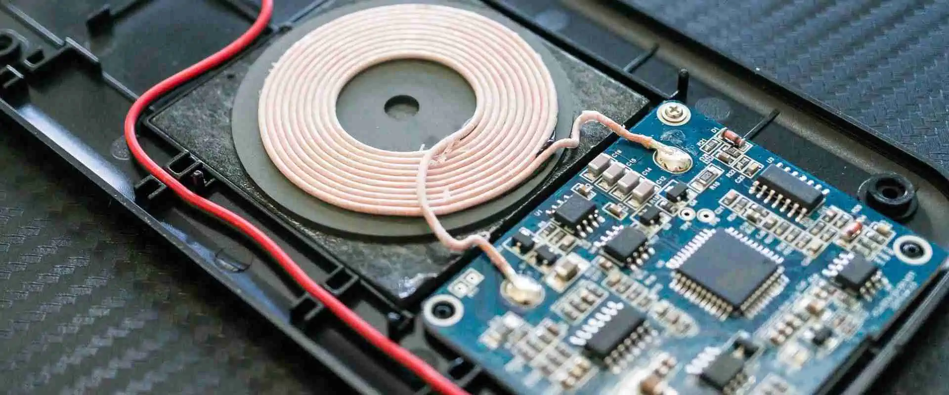
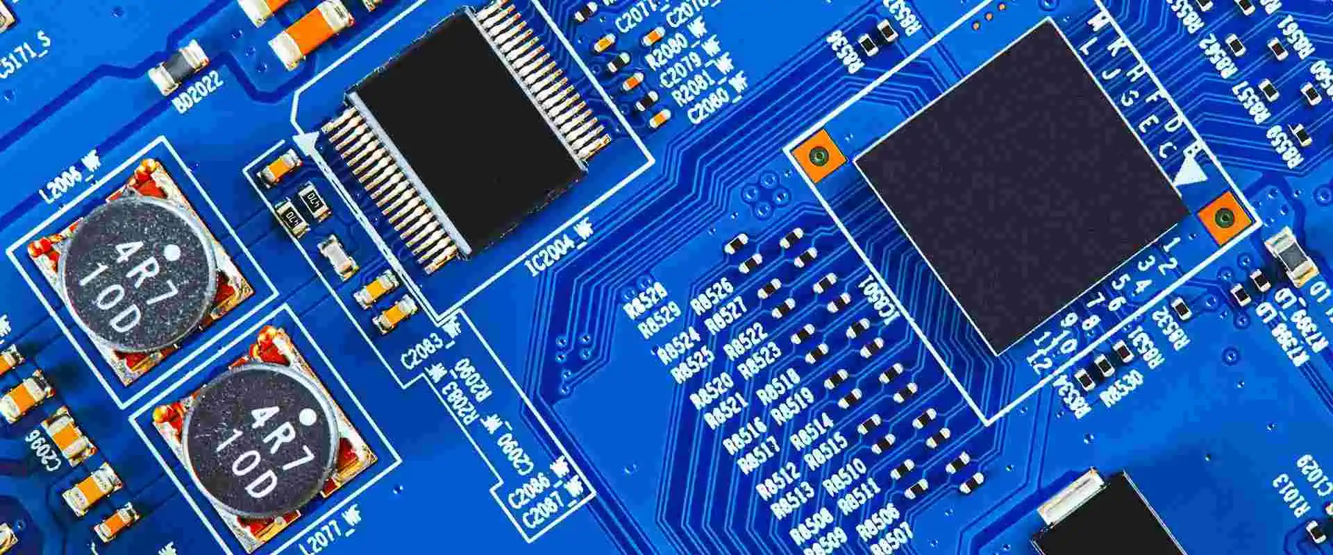
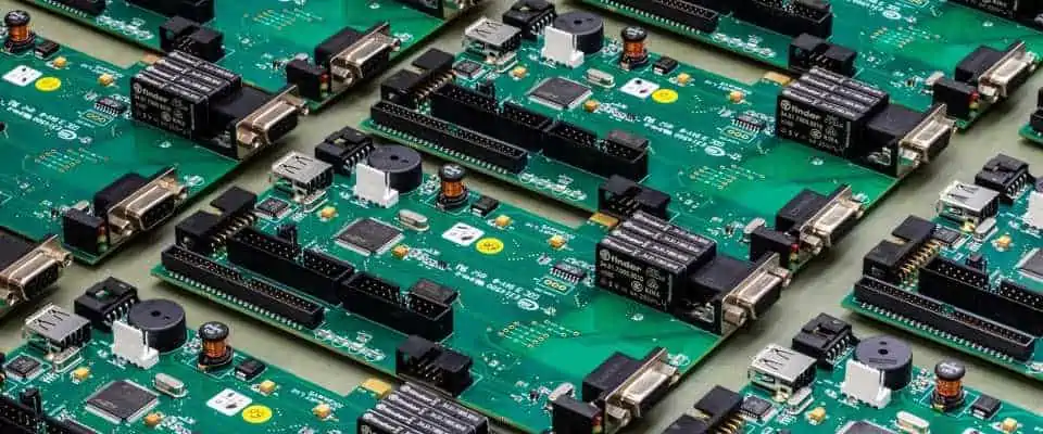
PCBs are the heart of any electronic device. Printed circuit boards (PCBs) are the basic building blocks of electronic circuits. They are the system’s brain where all the components connect and interact.

A PCB is a thin, flat board with copper tracks on it, on which you mount and connect electronic components to form an electrical circuit. They have thin boards, usually fiberglass, which provide the board’s core strength and resist breakage.

There are many different types of PCBs. You can make some PCBs from commercial off-the-shelf components (COTS). These components are available in pre-made forms. They are often less expensive than traditional PCBs.

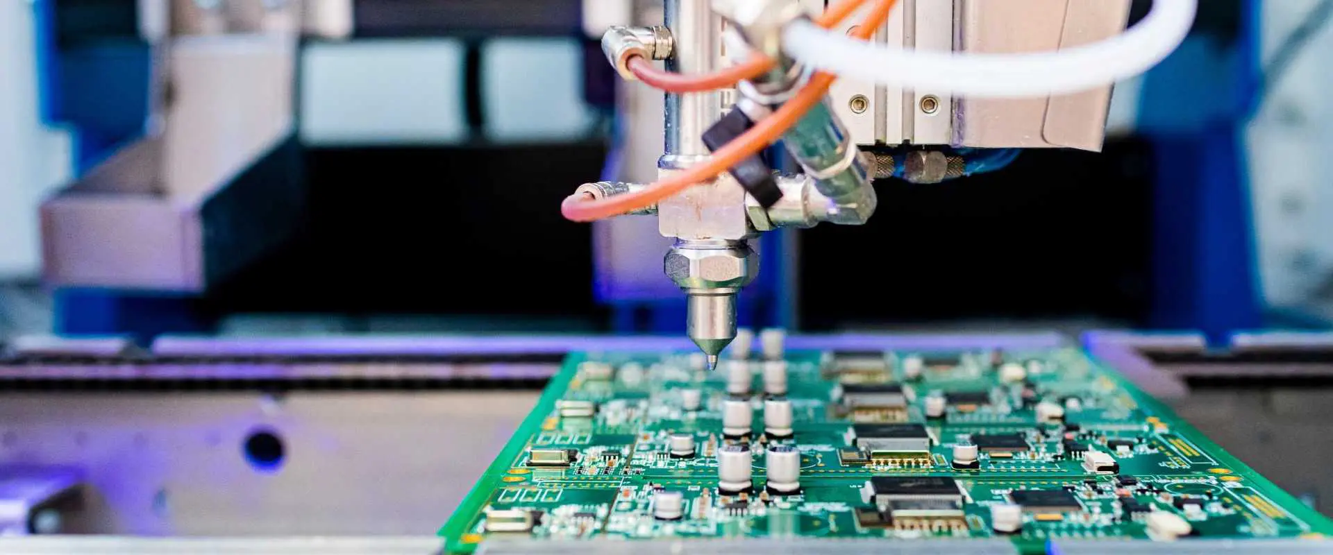
A common PCB industry trend is using autoplacers, which reduce the number of steps required to produce a PCB. This technology uses laser sensors to scan layers and compare a digital image to a Gerber file. The machine then marks the locations of the components with ink-jet writing.

There are many manufacturing processes and technologies used to manufacture PCBs. The process depends on PCB complexity, your technology, and a company’s production capacity.

PCB Manufacturing Processes:

  • Drilling
  • Soldering
  • Assembly
  • Lamination
  • Coating

These boards also undergo a thorough testing process. This test ensures that the board is functional.

PCB manufacturing is a complex process that requires a high level of expertise. In addition, PCB manufacturers must focus on quality at every stage of the process.

Printed circuit board manufacturing has significantly improved components’ size, track, and reliability. It also has made components cheaper and easier to produce. The Internet of Things (IoT) is also a growing trend. It enables wireless home connections and remote monitoring. This trend has increased the demand for smart, scalable devices.

How Video Electronics Affects PCB Industry

Printed circuit boards (PCBs) are critical components of many electrical devices. They are useful in everything from TVs to smartphones. They connect different components through a complex array of circuits. This allows them to provide advanced features.

Advances in 3D printing technology are impacting the PCB industry. These printers are smaller and more affordable. They are also eco-friendlier. There are expectations of increased demand for PCBs. Projections show that this market will grow at a CAGR of 3.3% until 2023.

The rapid development of consumer electronics drives the growth of the PCB market. The computer industry will continue to lead the market as the most common application for PCBs. However, the consumer electronics industry will also experience the highest growth.

The telecom industry uses PCBs in telecom towers, which transmit signals to cell phones. These towers need PCBs that can withstand outdoor environments. They also require PCBs for internal devices.

PCBs are useful in medical applications, including heart rate and blood glucose monitors. The industry is also experiencing increased demand for wearable electronics. We can incorporate these devices into clothing, sports helmets, and other accessories.

The medical industry is constantly developing uses for electronics. These devices are also becoming part of the Internet of Things. Various wearable electronics are now applicable in devices such as smartwatches. They also incorporate sensors, which monitor blind spots.

Advances in biodegradable PCBs are also impacting the PCB industry. This technology will also allow for more flexible PCB designs. It will also reduce the amount of components in a PCB. This will decrease the environmental impact of the electronics industry.

The demand for PCBs will continue to grow due to the increasing demand for high-speed data. However, the consumer electronics industry will experience the largest growth because of the increased demand for connected devices.

Challenges in Video Electronics Design

Various companies are taking their first plunges into the microfabrication scene. While some design engineers are well versed in microfabrication, others are still in the dark. The evolution of the microelectronics market is causing many companies to grapple with microfabrication for the first time. The resulting solutions can potentially improve a company’s bottom line, but taking the plunge requires careful thinking.

The best place to start is by defining the key roles and responsibilities of the various design reviewers. Next, the agency manager must communicate internally and with all reviewers to ensure everyone is on the same page. Finally, it will ensure a more efficient review process.

The best way to do this is to establish an open line of communication with all key reviewers, so that each is aware of the others’ viewpoint. This will also ensure that each reviewer has an opportunity to discuss their opinion and make a contribution.

The most obvious solution to this challenge is to hire a third party design house. These firms have the technical expertise and the know-how to design for you. In addition to video and audio, these companies offer a variety of other microelectronics and software solutions. The key to success is finding a design house with a deep understanding of the microelectronics space and a willingness to partner with you.

As a result of this partnership, you will take advantage of the best in class microelectronics solutions. This includes a high-end video processor from TI integrated with a Spartan-6 FPGA from Xilinx. This combination allows you to take advantage of the latest and greatest video and audio technology.

Why it is Hard to Design and Build a Working Circuit Board

Video device

Printed circuit boards are useful for mechanically supporting electronic components. They are typically composed of copper sheets laminated onto a non-conductive board. The circuit board is then assembled and wired with components.

If you plan to build a PCB, there are many things to know. One of them is how to minimize design problems. You can do this by using specific software and expertise. The best way to do it is to look for companies that offer a thorough DFM check.

EMI, or electromagnetic interference, refers to the unwanted effects of electromagnetic energy. It can cause problems with a circuit board’s function. One way to prevent EMI is to increase the ground area of the PCB. Another way is to compartmentalize the board. This means that some parts of the board are for power circuitry and others are for passive components.

If you plan to design a circuit board, you can start by drawing a schematic. There are several tools that you can use to draw a schematic. You can also use a schematic that someone else created. But you should be aware that a schematic is not a complete design. It simply contains information about the connections of components on the board.

After drawing a schematic, you can transfer it to a PCB. The best way to do this is to use a laser printer or photocopy machine. Another option is to print the schematic on magazine paper and then iron it onto the PCB board. Finally, you can paint the PCB board with a silkscreen, which can be any ink color.

Before soldering, you should clean the conductor area. You can use a soft cloth with no lint or use isopropyl alcohol to clean it.

Mousebites for separating boards from panels

Printed circuit boards are applicable in various consumer electronics, including computers, video games, TVs, cell phones, and home entertainment systems. To produce and assemble them, manufacturers need reliable boards that will meet the requirements of consumers. They also need low cost PCBs to meet the demand.

To get the most out of a PCB, it’s important to choose the right manufacturer. You need a manufacturer with a track record and experience. And Rayming Technology is your goo to PCB manufacturer. They have the right tools and know-how to prepare the PCB for assembly. In addition, they can customize the panel design to suit your company’s needs.

You must clean the PCB before each assembly. This is important to avoid liquid damage to the PCB. The design of the PCB is also important. Plan the layout of the holes to ensure that the components are firm.

It’s also important to have enough tabs to support the PCB. The tabs must be large enough to withstand the board’s weight and have a clean edge to avoid splintering.

The PCB needs testing. This will ensure that the mouse bites are not faulty and that you place the components in the right locations. It’s also a good idea to check for short circuits and defects in the copper layer. This will ensure that the mouse bites are the best PCB of all time.

Clean the PCB to prevent splattering liquid. You can achieve this with the use of hooks on the holes. It’s also a good idea to use a high-quality drill bit to ensure that you drill the holes as deep as possible.

Fingers

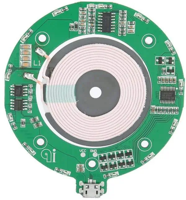
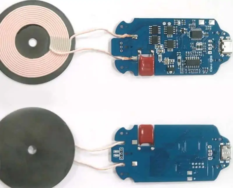
Printed Circuit Boards (PCBs) are good in video electronics to transfer signals. They help connect external devices to a PCB, enhance video graphics, and distribute digital signals.

A PCB gold finger is a gold-plated connector, or interconnection point, used to transfer signals. Gold has excellent conductivity and oxidation resistance, which prevents wear and tear on board edges.

We always standardize a PCB gold finger into a variety of thicknesses. Thinner fingers are good for prototypes and prototype boards, while thicker fingers are for boards needed in production.

Use Gold Fingers for connecting two boards or other peripheral devices to a motherboard. These connections are necessary for transferring signals and ensuring that a PCB does not wear out or fail. Gold Fingers can connect external speakers, scanners, and subwoofers to a PCB.

Gold Fingers should be able to handle up to 1,000 plug-out cycles. They should also have a smooth texture and no excess plating. They should never be near solder masks. Design them with great precision.

In addition to the standard thickness of 0.062 inches, PCB Gold Fingers should also contain 5 to 10 percent cobalt for increased rigidity. In addition, cobalt enhances the PCB gold finger’s ability to resist abrasion.

Making PCB gold fingers involves several steps, such as beveling, surface finish, and plating. The beveling process smoothens the edges of PCB Gold Fingers, which helps minimize sloping edges.

Automated optical inspection

Video electronic test

AOI or automated optical inspection is a visual inspection technique that uses light imaging. Automated inspection is becoming a major part of the PCB manufacturing industry. Using an AOI system is critical to ensuring that a product is of high quality.

An AOI system consists of an image capture system, a camera, and processing software. These components work together to provide the best possible image of the PCB assembly. The image capture system can consist of a single camera or several cameras. Using multiple cameras can provide more detailed imaging. The software controls allow the cameras to move to the proper position to maximize the quality of the imaging.

An AOI system can detect a variety of defects. For example, it can help to identify surface defects, open circuits, and thin solders. It can also detect poorly placed parts or shorts.

Various algorithms identify the errors. The AOI system then compares the image with the pattern from a good board. This gives the AOI system the information it needs to determine whether the assembly is defect-free.

AOI systems can be programmed to identify defects in PCB assemblies. To use an AOI system, the manufacturer must supply the specifications for an acceptable board. The specifications will serve as a gold standard during the inspection process.

An AOI system consists of a machine vision camera to capture an image of the PCB assembly. The processing software processes and analyzes this image before generating a product profile. You can compare this profile with the image of the golden board, which is known to be defect-free.

Electromagnetic compatibility

During PCB design, electromagnetic compatibility issues are typically responsible for re-design cycles. The good news is that there are some simple steps that you can take to improve PCB performance.

First, you should group the PCB components according to the type of signal they will carry. For example, designing a D/A converter should include analog PCB components. On the other hand, if you are designing a PCB that uses digital signal processing, you should include digital PCB components.

Second, you should route the signal traces properly. The length of the signal traces will determine how much electromagnetic interference it will carry. To avoid electromagnetic interference, keep the length of the signal traces short.

Third, you should decouple capacitors to avoid a large loop. A large loop can cause problems such as ringing.

Electromagnetic interference

EMI (electromagnetic interference) is a form of interference that disrupts the signaling in electronic devices. Natural or man-made sources can generate it. It can travel through space, plastic, insulators, or other materials. The interference can cause severe damage to electronic devices.

Two types of sources cause EMI: electromagnetic fields (electrical energy) and static discharges. Natural or man-made sources create electromagnetic fields, while static discharges result from any static source, including lightning.

Both types of interference have different characteristics. The most common type is continuous electromagnetic interference. This type occurs when a circuit is steadily running.

Lightning and switching systems produce impulse electromagnetic interference (EMI). However, you can reduce natural EMI by separating high-speed signals and filtering them to reduce their length.

Thermal expansion

Using a PCB in video electronics can mean high temperatures and associated problems. These issues can lead to circuit failures and even combustible substrates. The best way to avoid these problems is to select the right materials for your board.

The best material for your board depends on the type of circuitry and the frequency at which you will use it. The dielectric constant of the materials used to make your PCB is also a consideration. For example, titanium ceramics can have a higher dielectric constant.

The best way to minimize thermal expansion is to choose a high Tg matrix. The dielectric breakdown voltage of a material is also important. This is because it indicates how much voltage a material can handle before it breaks down.

Soldering techniques

Using PCBs in video electronics requires some soldering techniques. For starters, you need to have the proper tools to get the job done. You should also know your parts and how they are connected. If you don’t, you might end up with a mess.

The first step in soldering is to apply liquid flux to the PCB. This will remove any deposited oxides and make the board cleaner. Alternatively, you can use a flux pen.

Next, you must apply the correct solder amount to your component. You don’t want to put too much solder on your part, or you could end up with a short. This is where a multimeter comes in handy.

You may also need to use a piece of cardboard or silicone to hold your component. This will prevent it from getting all over your hands and keep your board flat.

PCB camera

Among the latest innovations in the field of camera electronics, the PCB camera is one of the most popular. The basis of this technology is the principle of electronic shuttering, which guarantees a unified image. It is common in surveillance systems and cellular phones.

PCB cameras have a picture sensor mounted directly on the camera board. The image sensor consists of a CCD (charge-coupled device) and CMOS (complementary metal oxide semiconductor). The CCD is a sensitive device that reacts to various electrical transients. A hermetically sealed chamber houses the CCD. This prevents condensation and allows for a wider range of detection.

The image sensor has an auto-exposure feature. The camera also uses several selectable lens types.

Conclusion: The Necessity of PCB Design for Video Electronics

PCB design is the backbone of any video electronics. Therefore, it is important to have a PCB design that you can customize according to the needs of the product. In this case, it is important to have a PCB design that you can customize according to the needs of the product. If there is an existing schematic or PCB design for a video product and if it can be modified to accommodate your project’s specific needs, use this rather than starting from zero.

Why You Should Opt For PCB Assembly Outsourcing

indian pcb manufacturer

Due to the growing demand for electronics by consumers, there has been a corresponding increase in the demand for PCB assembly services. Of course, it was the standard practice (and still is) for some OEMs to handle PCB assembling, but outsourcing PCB assembly accrues many benefits.

Itโ€™s, therefore, no surprise that companies are now looking to PCB assembly outsourcing to ensure they do not get overloaded on PCB assembling and miss-delivery schedules and lose customers as a result. This has induced an uptick in the number of companies dealing in PCB assembly outsourcing, and its benefits multiply by the day.

Should You Outsource Your PCB Assembly?

Outsourcing your PCB assembly is usually a good choice for new and old electronics manufacturers. From trying to match the costs of maintaining a manufacturing line to traversing the intricacy of PCB production, the advantages are just too many to count.

However, as with many sectors and industries, consistent quality benefits matter greatly, and this sector is no different. This article refreshes some definitions and highlights the benefits and processes of PCB assembly outsourcing.

What is PCB Simplified for a Beginner?

FULL PCB MANUFACTURING Quote

A PCB (printed circuit board) is a completely assembled circuit board with all the electronic circuitry devices needed to function effectively. These are unlike typical wiring boards used in standard electronics that do not offer complex functionalities.

What is a Printed Circuit Board Assembly?

This describes a completed board; after all processes, such as soldering and installation, have taken place on it. The pathways (conductive) etched in the laminated copper printed circuit boards are applied in a non-conductive substrate to create the assembly.

The last stage of the manufacturing process of a PCB design layout is adding electronic components to the boards. Only then can an electronic device be capable of performing its function.

Who Handles PCB Assembly Services?

A circuit board assembler handles PCB assembling. While their basic role is to solder electronic components such as (transistors, diodes, resistors, inductors, etc.), they also have to be able to recognize board patterns, follow sample boards correctly, and select electrical components.

In addition, they should know how to read wiring diagrams and handle tools needed for a quality finished product. All of this must be according to the important data in the product documentation.

How to Know Itโ€™s Time to Change Your PCB Assembly Outsourcing

PCB assembly outsourcing can be a tad difficult without the right PCB manufacturer. While your current supplier might seem like the best business partner you ever had (probably they offer some other services), you need to know when itโ€™s time to ditch that supplier for a new one. You must recognize and spot signs that itโ€™s time to change your supplier.

Below are some indicators and situations that can help you decide to change your supplier:

  • There is a general rumor about the scarcity of specific components making the rounds, and you need more news about it from your supplier. Either he is getting it somewhere else, or he has yet to learn what is happening.
  • You need to learn about how exactly your Printed Circuit Boards are manufactured. Your supplier deigns to inform you about how exactly he handles mass production. This answers your question of who is in control, you or your supplier.
  • Your deliveries, especially for medical projects, need to be on time, and production is getting less efficient. This might mean your supplier can no longer handle the agreed levels of delivery, or he is no longer working effectively.
  • You begin to receive more complaints about product defects and control devices, and more partners are returning defective items to such a vendor. This has to do with the quality of your products’ desired volume, which takes you back to your supplier.

What Are the Benefits of Outsourcing PCB Assembly?

Below are some reasons why you should opt for PCB assembly series outsourcing:

โ— Lesser Lead Times

There is so much good collaboration between contractors in numerous fields, which is no different in the PCB assembly industry. These long-lasting ties with their colleagues in the business can help you in a way. It can help you get your components faster and even allow for easy logistics once in a while. In other words, they can help you with lead times.

This is not a bad idea to handle all of these yourself, but you might get more benefits from using PCB contractors with more beneficial connections, and the network is, of course, more advantageous. The choice is yours anyway, like with low volume high mix or high mix low volume design modifications.

โ— Operating Cost Rationalization

Most SMT assembly for general manufacturing companies comprises far more than the costs of a manufacturing line and the staff required to run it properly. Experienced EMS companies that offer a legacy product usually have a better and well-structured environment for production than your own SMT assembly or any regular SMT assembly company that can assemble high-volume orders of parts in-house.

You will get good value for your money, even in tens of thousands or tens to hundreds, from shipping, storage, or procurement at a reduced cost of the PCB design you want. All of this is due to the beauty of specialization and the safety of inspection equipment at a lower cost.

Experienced and professional EMS are well-versed in cutting costs to manufacture and oversee assembly services for any business without sacrificing the quality of production batches or product versions.

Factors such as price and material availability disparities and short component life cycles must be handled equally and as smartly as possible. Mistakes at this stage are very costly, so highly experienced hands are needed.

Also, outsourcing your production to a proficient PCB contractor and suppliers of well-run SMT assembly services is a good choice for startups and low-capital organizations in this field. Not only will you get good inventory management, but you can also subscribe to product batch manufacturing because these company types depend on cash stored in material for a long while from time to time is crucial.

Conclusion

You may have an idle team on the ground and new and hungry machines ready to create all you need. Maybe you donโ€™t have one or understand how contract PCB fabrication works. Whichever way, you need solid PCB assembly services from a skilled electronics manufacturer like Rayming PCB & Assembly with proven system solutions and a short component life cycle you can trust.

If you need added advantages such as design assistance, ensure that the electronics manufacturer you choose can handle all that you need, and that means ensuring they can do what you need. Ensure you do your homework on your full-service PCB vendor.

Top 10 Companies to Manufacture semiconductor – Complete Guide

manufacture semiconductor

Semiconductors are big assets for different domains, so it is beneficial to learn about the products that function similarly to semiconductors for various devices and the giant companies that specialize in producing semiconductors. These are made from a fine substance called silicon. An extensive process is what manufactures extremely useful semiconductors. These include oxidation, metallic wiring, and many other crucial steps. 

In this post, we will explore the production process of semiconductors with all the essential steps in detail for better understanding. 

Steps in the Manufacturing Semiconductor Industry

1. Silicon Substrate Semiconducting Properties 

The initial step in producing semiconductors is to position them on each other to form a stack. It is a complex symmetry and a complicated structure. The main factor that makes the semiconductors strong and efficient is the silicon wafer chip. It is the foundation that makes the semiconductors serve long through their performance. This silicon which is useful for semiconductors is obtainable directly from the sand. Below is the detail of the process that extracts silicon from sand for the production of semiconductors. 

  • Collect a considerable amount of sand from melting, and then turn this sand into small or big crystals. 
  • This forms the ingots of silicon which are broad and heavy. Cut these ingots into fine wafer surfaces of silicon which are fragile and slim to appear. 
  • The upper layer of these ingots is not only uneven but also needs proper refining so that the circuitry that includes the semiconductor performs well on all counts. 
  • These wafers have a special line-based design on the upper layer. 

The average size of the silicon wafer processing determines the number of semiconductors. Small wafers cannot produce semiconductors in bulk. 

2. Oxidation 

Semiconductor Manufacturing Process

The silicon wafer produced recently does not contain the conductive ability. There is another process that makes these wafers conductive. It is a crucial step, and the slightest negligence in this step can ruin the ability of wafers. The process of oxidation is important for silicon wafers. Spray the oxygen in the form of vapors on these wafers, which creates a fine coating on these wafers. Now, this layer acts as a protective layer from water leakages and protects the circuits from sparks as well. Due to this fact, it is important to execute the process of oxidation on the wafers with complete vigilance and care to not compromise their functioning while on the circuit boards. 

3. Photolithography 

The step of photolithography refers to producing a design of the circuit with the help of water. It is identical to the process of capturing a photo from a camera. It includes a photo mask which is an important factor in the process of photolithography. There is a special computer that produces the design of the circuit in an efficient way. The photoresist is a material that actually produces circuit design on water. It gets applicable equally on the oxide layer present on the wafer when this substance comes into contact with the light. The light penetrates the photo mask. 

4. Etchin โ€“ Remove Unnecessary Materials

Etching means cleaning the wafer from unwanted residue and remains of the process so far. It helps in excluding the residue from the water layer just produced in the previous step. It ensures that only patterns are with the wafers. A special method of gas or liquid etching is useful to remove substances from the layers. There is a difference between both types of etching which is why it is important to consider both techniques before beginning to implement one of them. 

  • Wet Etching: It includes effective chemical substances only. 
  • Dry Etching: It includes plasma or gas in some cases for the process. 

Suppose there is a stack of semiconductors that is smaller than the width of a common paper. Both the steps of etching and photolithography are frequently executable on each layer present in this stack. There is also a fine insulator which is in the form of a film, that divides these layers to provide feasibility during these processes. It also protects the stack as well. The entire process is also identical to the production process of Multilayer printed circuit boards. 

5. Deposition & Implementation of Ion  

The deposition is the process that delivers a thin atomic layer on the wafer. There are several benefits to attaching this layer to the previous layers already present on a particular wafer. It is a feasible method and does not take much time as well, and It accurately attaches the deposition layer to the wafer. It is the main layer that provides the semiconductors with different electrical as well as conductive attributes. The process also includes a sub-step of ion implementation. A semiconductor also has some impurities due to the extensive process of manufacturing. All the abovementioned steps are important to give electrical and conductive attributes to these wafers so that they can work with several other circuits without any complications. 

6. Metal Wiring

Metallic wiring is important to make this entire set-up work which is why this should be done with utmost precision by the responsible technicians. This step conducts the electrical signals throughout the entire circuit. A clear and uninterrupted path is needed for the smooth current flow of the circuit. A thin layer of metals like titanium, tungsten, or others is also useful to conduct electricity in a flawless manner regarding the performance of the semiconductor in the future. 

7. EDS โ€“ Energy Dispersive Spectroscopy

The step is energy dispersive spectroscopy. This is a crucial step since it develops effective chip manufacturing of semiconductors. It can also be useful to eliminate faulty microchips that can create complications in the future while performing. The unit of yield is for measuring the relativity of prime chips as compared to one wafer on the basis of MCC or maximum chip count. This testing step is important to shortlist the best pieces for assembling into the circuit boards. 

8. Packaging in the semiconductor manufacturing process

Packaging is the step that winds up the production process. The whole structure of the previously produced wafers is divided into small chips that can be easily attached to an electronic device that functions with the help of a semiconductor. The chips that have been securely cut are then positioned on the printed circuit boards. The sub-step of bonding combines both the contact points of these chips and the substrates. Then another sub-step of molding gives these chips a proper shape that fits with the circuit boards. Then sealing and naming of these chips is important to differentiate them from others that have been produced. This mainly helps in shipping and delivering the semiconductors to the suppliers and direct clients. 

Top Best Semiconductor Manufacturing Companies

FULL PCB MANUFACTURING Quote

1. Intel 

Intel operates from California. It has been a giant producer of semiconductors for many years. It houses a huge workforce of employees and technicians, which are spread around 45-46 countries. The famous product of Intel is the X86 microprocessor and its other variants. These are important for the smooth functioning of laptops and other similar devices. These processors get assembled in the devices of Lenovo, HP, and many more. There are motherboards, integrated circuits, graphics chips, and others delivered and produced by the company. The company is reliable to get in touch with regarding such services. 

2. Samsung Electronics

Samsung is a Korean producer of world-class electronics. The most famous of them are Samsung smartphones and smartwatches. It has been operational for many years and provides consumers with extraordinary electronic appliances. The semiconductors of the company are exceptional in their functioning. These semiconductors are present in tablets as well. The company has a solid stance among the pool of electronic producers, which makes it reliable for new consumers on all counts. 

3. (TSMC) Taiwan Semiconductor Manufacturing Company

It is on the list of major producers of semiconductors and relevant chips. It is a standalone producer of these chips in Taiwan, which is an impressive factor about the company. These semiconductors are useful for Apple products and others. The company has also been successful in generating decent revenue through the delivery of its well-produced semiconductors and chips.ย 

4. SK Hynix Inc

This is a special agency to produce memory semiconductors which are important for electronic gadgets. It is functional in South Korea and has different offices in many regions of the globe. There is a large workforce that handles the company and its global operations. The clients of the company are Apple, Dell, and HP. The other products offered by the company are smartphones and CD players, along with others. All of its products have no parallel in performance, durability, and precision. 

5. Broadcom Corporation

It is an American manufacturer of semiconductors that have been functional for many years. Their semiconductors are useful to be installed in mobile phones, PCs, and many other devices. The company produces encryption-based chips, which are helpful in the domains of E-commerce and defense. The main objective of these chips is to accelerate the functions of the electronic devices they are attached to. A special series offered by the company delivers uninterrupted WiFi, which is an important feature in mobile phones. These chips are also supportive of different brands like Android and Apple. 

6. Qualcomm

The products of Qualcomm are not only wireless but also helpful in the domain of software development and implementation. These services are the main character for the progress and solid stance of the company. The company offers not only semiconductors but also laptops and transportation equipment for its consumers. The first ever chip produced by the company was Centriq 240. Its success and acceptance among consumers empowered the company to produce more chips identical and different from this flagship chip that address the problems of digital users. 

7. Micron Technology

The company operates from Idaho. Its specialty is semiconductors, and it also offers services that enhance data storage for consumers. These devices are effective in securing personal data on computers. Also, the semiconductors produced by Micron are useful when it comes to precise functioning. The agency is a giant and houses many employees who are all adept and devoted to their responsibilities. There have been some incredible innovations brought to light by the company. These are microSD cards with exceptional storage capacity.  

8. Applied Materials

It is another good producer of semiconductors. They specialize in electronic gadgets, computer accessories, mobile phones, and other devices. These also deliver the raw materials needed for the production of the chips of semiconductors. These are also important for the production of useful coatings and layers needed for some devices. The company is reliable when it comes to its claims and services. It is also one sole reason to provide feasibility to the consumers on all counts. 

9. Nvidia Corporation

It is another producer that operates from California. The company produces not only remarkable semiconductors and relevant chips for them but also manufactures graphic processing units as per the orders of the clients and the needs of the consumers. These are inevitable for gaming computers which contain some extra and unique features as compared to other computers. The most renowned processing unit from Nvidia is the GeForce RTX 3060 Ti which is on top of the dependable GPUs for gaming enthusiasts. The company is also important to consider for supercomputing websites that are highly active around the globe. The processors of the company are useful for mobile phones, tablets, and other devices for daily usage. 

10. Texas Instruments Inc.

Texas Instruments (TI) is a seasoned player in the game. It is among the most experienced producers of semiconductors for consumers. The company works with the help of a large workforce, which is the backbone of the company. The main products are the special embedded processors and also analog chips and microchips, along with the production of useful semiconductors. The products offered by the company are accessible and are supportive of all types of devices, no matter the software. The company itself is a major supporter of the industry. There have been several successful devices produced by the company that laid the foundation for the modern production of tech-based electronics. These are transistors and calculators. 

Reasons Why Manufacturing Semiconductors Is Essential

semiconductor manufacturing machine

There is no doubt in the fact that several authorities have reported the downfall and deficit of semiconductors in the industry. There are many reasons for it. These factors can greatly impact the perspective of using semiconductors in a laymanโ€™s life. These induce power in all the electronic appliances that might be portable or not. Whether it is a small device like a mobile phone or a giant device like a plane, semiconductors are equally beneficial for their performance. These devices have actually helped technology evolve to a large extent. These are responsible for the amount of progress and joy we all have experienced over the last years through the existence of technology. In this section, we will learn why semiconductors are important for smooth work-life balance and typical electronic devices. 

Why are Semiconductor Manufacturing Processes Essential?

In the past days, computers were the only devices that were reliable for people. These were invented way before the early silicon oxide film microchips. Computers were big in size and also consumed a huge amount of power all the time for proper functioning. Semiconductors became a good alternative to fussy computers. These were quick to produce, function, and more reliable than others. These were more affordable than computers. The adjustable shapes and sizes of these semiconductors helped in the astonishing emergence of mobile phones, smartwatches, and other gear, which developed a whole industry of electronics for producers, suppliers, and consumers. It is important to know about those sectors which cannot survive without semiconductors. 

Industries Count on Semiconductor Manufacturers 

All sorts of machines with variable magnitudes work with semiconductors. These chips are important for their fine performance. These semiconductors are important for internet connections, automobiles, and smart devices, which are commonly used by every other consumer. Below are some important sectors which completely depend on semiconductors for their well-being and commercial progress at the same time. It is not wrong to say that these sectors have the ability to generate bigger revenue due to the existence of semiconductors and pertinent chips. 

  • Computing

The most integral domain which relies on semiconductors is computing. The chips, like semiconductors, are integral to developing strong connections between the servers and the clients. These work with the help of a binary code to give directions to the instructions of the users. It can be either for downloading something or saving a file on the computer. Typical types of semiconductors used in the computing industry are GPUs and microprocessors. These are designed to assist the devices in non-jarring performance. These secure the battery life and maintain the performance as well. 

  • Telecommunication

The semiconductors function similarly to the computing industry for telecommunicate operations. The goal is to regulate machine-based activities. This can also vary according to the type of semiconductor chip used for a certain operation. The patterns also vary from one electronic to the other. The chips for mobile phones have the ability to smooth out navigation, battery life, and many other features. The function of these chips is also different when it comes to overall performance. Other devices used in the telecommunication field also include such chips for effective functioning.

  • Household Appliances

Typical household electronic appliances like washing machines, microwaves, ACs, and others cannot work properly without semiconductors. These semiconductors render different features like temperature regulation, automation, and timing functions, all due to the installment of semiconductors in these devices. These have made the functioning of home appliances easier. So that these can contribute to making the life of users more feasible, these chips are being evolved at a rapid pace, and the bar of their excellence is rising at the same time to meet the expectations of the clients.

  • Banking

Semiconductors are also helpful in banking operations. These are tech-based and ease the hectic banking activities for the officials and the customers as well. Banks are among the top investors of semiconductors owing to their benefits on a regular basis. These rely on expanding chip manufacturing for flawless operations. The computers for digital interaction, accounting activities, and others related to banking are all feasible due to semiconductors. These can prove to be beneficial when installed in surveillance cameras and ATMs when enhanced technically. 

  • Security

The field of security can gain huge advantages by using semiconductors. These can be used in alarm systems, security equipment, and locking systems to ensure complete security and protection of the premises regarding houses and offices. These are tech-based, which makes them effective in sending quick alerts to the users through their computers and mobile phones if someone sneaks into their premises discreetly.

  • Healthcare

Healthcare is another big fan of semiconductors. It is true that healthcare centers and hospitals implement cutting-edge technologies for different purposes. The medical equipment that uses semiconductors is not only reliable and durable but also performs quick surgeries and diagnoses, which save the lives of hundreds of patients daily. These are accurate pacemakers, monitors, diagnostic machines, scanners, and many more. The chip production of semiconductors in these machines is for enhancing the features like scanning fingerprints, hands, temperatures, patientโ€™s vitals, and much other stuff regarding the health of a patient. 

Final Thoughts 

The existence of semiconductors is important for daily survival. These have transformed a complex life into a much simpler one for millions of people. These are also beneficial for the essence of life and regular commute. Plus, the activities related to office and home are equally feasible due to the effective performance of these semiconductors through various devices. 

In this post, we have learned about some major producers of semiconductors and the industries where semiconductors are mostly used for the daily survival of consumers. So that technical complications can be kept at bay that can be irreversible later. 

Your Guide to Getting the STM32F427VIT6 32-Bit Microcontroller

STM32F427VIT6

STM32F427VIT6 is a 32-bit single-core Microcontroller (MCU). It is designed for the low-power applications.  This MCU is also used with a variety of applications or devices, such as home audio appliances, motor drive and application control devices and alarm systems.

In this article, we cover the STM32F427VIT6 extensively, talking about the function of its 32-bit core processor and every other thing in-between.

STM32F427VIT6 is a User-Centric MCU

Microcontrollers are those semiconductor devices used for enabling user-based configuration of the logic elements. It is therefore, not a surprise that the STM32F427VIT6 inherits the same characteristic, as it is a fully user-programmable MCU.

That is why you can optimize it for a wide range of applications, ranging from alarm systems, printers, medical equipment, scanners and HVAC systems.

Another aspect of STM32F427VIT6โ€™s user-programmability is the compatibility with the STM32F2xx devices โ€“ which is the family of Microcontrollers (MCUs) from where it came from.

We also want to point out that STM32F427VIT6โ€™s functionality is largely buoyed by the 32-bit single-core Microcontroller (MCU) architecture.

According to the manufacturer, this core is derived from the wider Arm Cortex-M4 CPU, which comes with a combination of Floating Point Unit (FPU), and an Adaptive Real-Time Accelerator (ART).

From the above, one can say that the STM32F427VIT6, besides being fully user-programmable, it also designed to facilitate the MCUโ€™s functions.

The 32-Bit Architecture

FULL PCB MANUFACTURING Quote

One would think that the 32-Bit single-core on the STM32F427VIT6 is the only point where a 32-bit would be used on this MCU.

Interestingly, this type of bit is also used in a number of other places. For example, there is a 32-bit RISC processor attached to the Arm Cortex, from where STM32F427VIT6 is able to deliver the highest levels of performances expected of a Microcontroller (MCU) powered by this type of processor.

There is also a 32-bit data word that serves as the โ€œderivative pointโ€ for the Cyclic Redundancy Check (CRC).

For emphasis, the CRC is a protective feature on STM32F427VIT6, which is designed to verify the transmission and storage of data on this Microcontroller (MCU).

The calculation unit needed by the CRC to do that is to be derived from both a fixed generator polynomial and the 32-bit data word.

The Multi-AHB Bus Matrix

The 32-bit architecture is also deployed for use with the Multi-AHB Bus Matrix. The function or role here is to be the โ€œinterconnectorโ€ that combines all the major peripherals (masters), such as the USB HS, CPU, DMA2D, DMAs, LCD-TFT, and Ethernet.

The interconnection made here is designed to help both the aforementioned master (peripherals) and the slave (peripherals) to be connected. Examples of the slaves connected to the masters are:

  • APB
  • Flash Memory
  • AHB
  • RAM
  • FMC

The interconnection made via the Multi-AHB Bus Matrix allows for the aforementioned peripherals (both the masters and the slaves) to be optimized for the highest levels of speedy functions.

Robust Application Security

It wouldnโ€™t be worth it if the Microcontroller (MCU) doesnโ€™t โ€œspeed things up.โ€ For that reason, STM32F427VIT6 has been optimized to offer the highest performance levels, such as the protection of the target applications.

A combination of the Memory Protection Unit (MPU) and the full set of DSP instructions are required to further enhance the target applicationsโ€™ security.

STM32F427VIT6 is Designed for the Latest Embedded Applications

Newer technologies and operating modules are rolled out as the days go by. When it comes to MCUs, the configuration processes and techniques have to be top-notch to assure of the devicesโ€™ capabilities.

The basis of the STM32F427VIT6 on the Arm Cortex-M4 core processor with the Floating Point Unit (FPU) is a major step to that end. The combined function of the processor and the FPU allows for the real-time application and or implementation of all that the STM32F427VIT6 MCU has to offer.

Besides, this dual architecture is also responsible for STM32F427VIT6โ€™s capability to provide a low-cost MCU development platform, cut down on design iterations through the advanced response to interrupts and offer an improved computational performance.

STM32F427VIT6 also boasts of one of the lowest-cost Microcontroller (MCU) architectures because of the dramatic reduction of the pins and the overall reduction of excessive power/current usage.

Program Memory

Different memory types are used to program a Microcontroller (MCU). The choice has to do with the target applications, the extent of the applications and the data reading mode.

STM32F427VIT6 packs a punch of those with the integration of the Flash program memory type. Flash is a type of non-volatile memory used in most semiconductor devices. The Flash memory offers data reprogramming and erasing.

On the STM32F427VIT6, it offers much more than that โ€“ it can also be embedded to the device. The embeddable nature of the Flash program memory allows for the storage of both programs and data/wireless information.

Interestingly, the Flash memory, despite the non-volatility, also offers fast data processing, up to 2 Megabytes per second (Mbps).

STM32F427VIT6 Uses DMA for Memory Management

The Flash program memory allows for fast data transfer, but much more can be done to that end. STM32F427VIT6 uses the DMA Controller (DMA) to achieve a more stable and facilitated data transfer process.

The core attributes of the DMAโ€™s functions to the STM32F427VIT6 include:

  • Dual configuration by software and the hardware connected to the DMA Controller to handle the DMA requests.
  • The support of two general-purpose dual-ports DMA on the STM32F427VIT6. The DMA1 and the DMA2 helps the MCU to manage different memory functions by leveraging the 8 streams attached to each of the DMAs. It is therefore, through this connection that STM32F427VIT6 can handle the memory-to-peripheral, memory-to-memory and peripheral-to-memory data-induced transfers, almost at the same time.

Conclusion: STM32F427VIT6 Achieves a Balanced Performance Via the ART Architecture

STM32F427VIT6โ€™s Adaptive Real-Time Accelerator (ART) is a concise architecture for scaling this Microcontroller (MCU)โ€™s functions.

It functions or works by optimizing its memory accelerator to align with STM32F427VIT6โ€™s Art Cortex Floating Point Unit (FPU)โ€™s processors.

The optimization made here sees to the dual function of the two to achieve an increased program execution speed, from the 128-bit Flash memory.

ISL81387IAZ: A Dual Protocol Transceiver with ESD Protection

ISL81387IAZ

ISL81387IAZ is a dual protocol transceiver, ideal for configuring devices based on the RS-232 and RS-485 standards.

This blog post will help you understand how the dual protocol works.

User-Based Configurations

ISL81387IAZ is a user-configurable BiCMOS interface Integrated Circuit (IC). It can be configured to fit into a variety of performances, including the RS-232 transceiver, RS-422 and the RS-485 differential transceiver.

Power Management

Balancing the performance and power usage of a transceiver are two important considerations. We are pleased to see that ISL81387IAZ has some measures in place to help this function better.

For example, the low-current shutdown modeย is an excellent solution, as it can turn off the device once it goes below 35ยตA.

Board Layout Simplicity

FULL PCB MANUFACTURING Quote

ISL81387IAZ also has a dedicated feature called true flow-through pinouts. These pinouts help the transceiver in offering the best mapping or layout for configurations.

ISL81387IAZ also supports the loopback mode; a function that allows for the self-testing of the circuit board functions.

The loopback mode also helps in keeping the transceiver active. For example, it comes in handy to keep the outputs connected to the loads during the loopback function. That way, connection-related issues, such as shorted cables or connections can be easily detected during the operation.

Problem-Free Communications

By โ€œproblem-free communications,โ€ we refer to the data transfer rate. ISL81387IAZโ€™s data transfer rate is between 115kbps and 20 Mbps. Both of these are user-programmable and comply with the RS-485 transmitter mode.

The transmitter supports up to three (3) data rates, which are both slew rate limited.

Open-Short Function

Also called the full fail-safe operation, the open-short function is one feature that keeps this transceiver active. The activeness is culled from the ability to keep the Rx output in a high state, especially if the inputs are shorted or opened together.

The RS-485 Mode

ISL81387IAZ can be configured through any of the modes, as it is a dual protocol transceiver. The RS-485 mode is one of such modes and it offers additional features to the transceiver. Here are some of these features:

Charge Pump Disabling

When the ISL81387IAZ is in the RS-485 mode, it often disables the charge pump. For emphasis, the charge pump is often activated during the RS-232 mode usage, as it aids the generation of the compliant ยฑ5 Tx output levels.

However, once the RS-485 mode is active, the charge pumpโ€™s capacitors is eliminated, likewise the charge pump is disabled.

Low Noise

The disabling of the charge pump also leads to lesser noise during the transceiverโ€™s operations. Besides, ISL81387IAZ has a general noise-limiting capability, via the large (2.7-volt) differential VOUT. This function can improve the noise immunity capabilities of the RS-422 and RS-485 networks/modes.

Power-Savings

Since the charge pump is active, it tends to consume more power. By disabling and eliminating the further usage, the RS-485 mode saves more power in the process.

Packaging as a Performance Catalyst

ISL81387IAZ uses a QFN package/case โ€“ and that serves as a boost to the performance. These are some of the catalyst-like features:

1. Pin Flexibility

The QFN package/case uses a combination of the active high and the low Rx outputs. This function enables the pins to have an increased flexibility; up to the point that the combined function of the DEN and RXEN functions allow the Tx/Rx directional control via a single signal.

2. Lower Speed

The QFN package supports a lower speed and an edge rate option, capable of clocking 115 kilobytes per second. The combined function of the edge rate option and the lower speed are ideal for making ISL81387IAZ ideal for longer bus lengths or optimization for EMI-sensitive designs.

3. Supply Voltage Compatibility

As a way of making the supply voltage compatible, the QFN package has been optimized along the lines of logic supply voltage pin (VL). The pin makes the package ideal for enabling the VOHย level of logic outputs. By enabling this, it becomes easier to combine the switching points of the logic inputs compatible with the supply voltage in another mixed voltage system.

Product Attributes

Here is a tabulated breakdown of all of the components making up ISL81387IAZโ€™s dual protocol transceiver:

AttributesDescription
DuplexHalf
TypeTransceiver
Operating TemperatureBetween -40หšC and 85หšC
Voltage โ€“ Supply (minimum to maximum)Between 4.5 volts and 5.5 volts
Supported ProtocolsRS-485, RS-232 and RS-422
Mounting StyleSurface Mount Technology (SMT)
Data (transfer) Rate20Mbps
Number of Supported Receivers and Drivers2/2
Receiver Hysteresis35 mV

Important Points to Note about ISL81387IAZโ€™s Dual Protocol Architecture

Transceivers are dedicated devices that necessary hardware resources to enable the real-time communication of devices over an extended cable length or trace length.

4. The Need to Find a Balance in Transceiver Performance

The major industrial interfaces used in ISL81387IAZ are the RS-232 and the RS-485 standards. The two offer improved functions and that is why they have been combined inside the ISL81387IAZ transceiver.

On the one hand, we have the RS-232, a transceiver interface standard that became popular in the early 60s. It works by providing a single-ended, full-duplex interface to enable point-based consumer electronics communication. The RS-232 interface standard also combines receiver grounds and ground wire connection to facilitate a common interface for receiving and transmitting (data) signals.

On the other hand, we have the RS-485 interface standard, which became popular in the early 1980s. The most outstanding function is the drastic improvements made in the data transmission, across longer distances โ€“ and even in noisy environments and working conditions.

Those are the basics. Why were the RS-232 and RS-485 interface standards combined? The formation of a dual protocol interface with the two is because of the need to combine the two interfacesโ€™ functions, as both of them have viable functions to offer.

Through this combined function, the interfaces now offer individualized solutions. For example, the RS-232 interface standard helps in the following ways:

  • Enabling interface connection to either the single network or extended over long distances.
  • It enables an easy routing of signal traces to the local controllers.
  • The RS-232 interface standard also boosts the data rates, up to 400kbps. It does it excellently, without exceeding or going above the recommended, maximum slew rates.

On the other hand, the integration of the RS-485 interface standards makes the following contributions to the ISL81387IAZ dual protocol transceiver:

  • Implementation of a high-speed mode.
  • It supports the networking of up to 32 unit loads via a multi-point bus topology.

Wrapping Up

ISL81387IAZ combines the RS-232 and the RS-485 interface standards to make the transceiver flexible and versatile. The versatility is derived from the local controllerโ€™s capability of acting independently as an interface converter or driving the different bus systems.

All you need to know about Printed Electronics Manufacturers

PCBA Conformal coating

Printed electronics manufacturing is a huge industry that is a big part of the electronics market. PCBs are also helpful in a wide range of applications, including displays and sensors for carbon monoxide, ozone, alcohol, hydrogen sulfide, and nitrogen dioxide.

Printed Electronics Technology

Printed electronics technology is the process of creating electronic circuits on flexible substrates. It is a new technology that combines the benefits of traditional additive manufacturing techniques with the advantages of new materials. In addition, it is an environmentally-friendly, time-saving, and conformal manufacturing method.

Printed electronics technologies include screen printing, gravure printing, flexographic printing, and inkjet printing. Each printing method can produce a layer thickness of up to 20 mm. Screen printing is excellent for printing thicker prints.

Printed electronics are in a wide array of applications in traditional industries such as automobiles and transportation. However, they are still in the early stages of development.

Printed Electronics Companies

FULL PCB MANUFACTURING Quote

Printed Electronics companies include those that develop electronic circuits and devices by using additive fabrication methods. These suppliers also include those that manufacture printed circuit boards. Some top players in the Printed Electronics market include Rayming Technologies, NovaCentrix, Palo Alto Research Center Incorporated, E Ink Holdings Inc., Thin Film Electronics, Inc., and BASF SE.

Printed Electronics is a growing market with new products coming on line and a competitive landscape that includes top players. The market consists of a variety of applications, including Smart Media Products.

APAC is a key market for printed electronics. Its rapid industrialization and urbanization are helping drive the market’s growth. This region accounted for 44.6% of the global market in 2021. The region is one of the world’s largest consumer goods and industrial product producers. China is also experiencing rapid growth in the market.

The leading provider in the Printed Electronics market has adopted product launch strategies to gain growth in APAC. They include LG Display Co., Ltd., Samsung Electronics Co., Ltd., and Epson of Japan.

Golden Valley Products has a rich history in the printed electronics market. It manufactures high-quality, highly durable printed electronics for the automotive and medical industries.

Blue Spark Technologies is a printed electronics company founded in 2002 as Thin Battery Technologies. Its customer base includes manufacturers, integrators, and product designers. It develops proprietary power sources for its products.

T-ink has applied printed electronics to self-heating apparel, car weight reduction, and secret military equipment. It also works with Hallmark on interactive tablecloths and pillow radios for Toys ‘R’ Us.

Printed Electronics Solutions

Printed electronics solutions are an emerging field of additive manufacturing. Technology can make electronics cheaper, more flexible, and easy to integrate. It also makes it easier to design electronics on a large scale.

These materials need to be able to provide improved electrical performance and processability. The materials also need to be chemically compatible. They also need to be stable in terms of environmental stability.

Printed electronics solutions are also becoming more critical as the Internet of Things develops. Objects integrate with sensors and tags that gather information and share it with the cloud.

Printed electronics solutions offer a unique way to manufacture large-scale electronics at low costs. In addition, they can be highly automated to keep labor costs down.

The display segment led the largest printed electronics market share in 2020

Printed electronics are electrical devices that we print on a substrate. The technology uses less energy and is exceptionally lightweight, bendable, and shatterproof. This technology also provides cost efficiency, dependability, and low maintenance requirements.

The demand for printed electronics is increasing due to many advantages. As a result, the market will reach USD 44.4 billion by 2030. The major drivers of the market include the increasing application of printing technologies, increasing demand for thinner electronics, and mass production costs. In addition, the market will grow at a rate of 18.5% from 2021 to 2030.

The increasing popularity of advanced consumer electronics products largely drives the demand for PCBs in the consumer electronics sector. In addition, the market is growing faster in the forecast period due to increased investments in R&D activities. In addition, the rising use of IoT devices will create new growth opportunities for the market.

Screen printing vs. inkjet printing

We can produce Printed electronics with several different processes, such as screen printing or inkjet. These techniques differ in their advantages, challenges, and cost.

Screen printing is the most common technique used in manufacturing PCBs. It involves the transfer of conductive inks onto a substrate through a finely woven mesh. The non-conductive inks are solvent-based or UV-curable. This technique has many advantages and can be adapted to meet many different requirements.

Screen printing is an established technology that has been helpful for centuries. However, it is unsuitable for hazardous environments or for people uncomfortable with chemicals. It can also be significantly cheaper than other printing technologies.

Gravure printing process

Printed electronics is a technology that uses printing processes to create electronic devices. It is a highly versatile process used to make a wide range of electronic devices. The process produces a thin layer of ink applied to a substrate.

Gravure printing is a technique that uses a copper cylinder and a steel coating to transfer ink to a substrate. The process has significant advantages over competing print processes. The speed and simplicity of the process make it ideal for large-scale, long press runs. It also excels at producing the world’s smallest precision objects.

Printed sensors for carbon monoxide, ozone, alcohol, hydrogen sulfide, and nitrogen dioxide

Printed sensors help to measure gaseous compounds such as carbon monoxide (CO), ozone, alcohol, hydrogen sulfide (H2S), and nitrogen dioxide (NO2). The sensors depend on a wide range of transduction elements. They connect to a microcontroller. These sensors are helpful for indoor air quality monitoring. They help to detect flammable, combustible, and other toxic gases. They are mainly essential in surface mount technology applications.

Optimizing its active sites can enhance the sensing performance of the sensor. Moreover, the structure should be designed in such a way that it has high adsorption capacity and high conductivity. We can achieve this by incorporating MOFs with polymeric materials.

Moreover, polymeric materials have high electrical conductivity and great surface area. These features make them an excellent material for developing innovative nanohybrid sensors.

Factors Pushing the Growth of Electronics Manufacturers

Electronics-Assembly-Companies-in-Turkey

Electronics manufacturers are implementing technology into different products, including consumer, industrial, and medical electronics. Multiple applications include smart packaging, smart labels, and smart sensors. These devices enable quality control, alert patients about medicine dosages, and help healthcare professionals monitor patients remotely.

PCBs can produce thin, flexible shapes, allowing manufacturers to create low-cost sensors. This technology is gaining popularity in the automobile industry, e-readers, and smart glasses. The technology also creates smart labels, providing call-to-action information and alerting patients to medicine dosages. The industry leader also sees increasing demand for smart packaging equipped with NFC chips. This technology will be a quick replacement for traditional packaging.

APAC is a key market for electronics manufacturers. It is home to growing semiconductor and large electronics manufacturing industries. It is also experiencing rapid urbanization and industrialization, which will contribute to its growth. As a result, electronics manufacturers focus on emerging markets, such as Asia Pacific, to expand their reach. In addition, many manufacturers focus on product launches and distribution partnerships to increase their regional presence.

Electronics manufacturers are using new technologies requiring specialized machinery and personnel development. Emerging technologies also require a large investment in research and development since the cost of new materials and equipment is high. As a result, manufacturers must focus on producing robust products and lightweight materials to drive growth.

Flexible electronics are crucial to the electrification of vehicles

Increasingly, researchers are exploring the potential applications of flexible electronics in the automotive industry. This technology includes electronic displays, sensors, logic/memory applications, and photovoltaics. These devices include flexible materials, such as plastic, paper, metal foil, and flex glass.

Using nature-derived materials for flexible electronics is a great way to benefit the environment. It is also beneficial to the development of electronics. Moreover, these materials can have intriguing properties.

Flexible electronics are designed to be flexible, bendable, and stretchable. This means they can be helpful in clothing, medical devices, or consumer products. For example, a new flexible electronic circuit could move with the user’s body, staying in place without adhesive. In addition, we can use it to develop interactive wallpapers that double as touchscreen displays.

Some of the most demanding applications of flexible electronics are solid-state lighting applications. These include OLEDs or organic light-emitting diodes. OLEDs display digital information on television screens.

Developing suitable processes for the manufacturing of flexible electronic components is essential for the development of this industry. These processes will also make flexible electronics more convenient to use and interact with.

Low-cost processes

Printed electronics are electronic devices we fabricate partially or fully on a substrate. They have a lower carbon footprint and are recyclable. They can manufacture custom parts or designs. This technology is attracting attention in the electronics industry.

Printing electronics can create all electronic components, including light-emitting diodes (LEDs), batteries, and radio frequency identification (RFID) devices. Conductive inks and substrates used to print electronics include synthetic or natural polymers. PCBs are helpful in various applications, including the healthcare, consumer electronics, and automobile industries.

Printed electronics can include many capabilities, including flexible substrates and biodegradable materials. As a result, the market opportunities for PCBs are growing at a fast pace. It is also attracting the attention of academia and industry.

Printing technologies have enabled manufacturers to design new structures that were previously impossible. It also has facilitated the use of unorthodox materials. This strategy allows manufacturers to create cost-effective small production runs to produce customized customer solutions.

Changing the viscosity of an ink

Changing the viscosity of the ink is a driver of growth for electronics manufacturers. Inkjet printers are ideal for low-viscosity materials. Therefore, the inkjet segment will witness a substantial growth rate over the forecast period.

Increasing the solid content of ink also decreases the sintering temperature. However, higher sintering temperatures can cause metal precipitation. In addition, the annealing process may require higher temperatures and longer processing times.

Printing printed electronics requires coordinated development of ink supplies and printing processes. Inks belong to conjugated polymers, charge transfer complexes, and organic metal chelates. Some inks can be used in high-performance applications, while others can help in low-performance applications. Depending on the application, the ink can be used for printing, squeezing, gravure, screen printing, and offset lithography.