The Xilinx Zynq System-on-Chip combines an ARM Cortex-A9 dual-core processor with programmable logic fabric and is a flexible and high-performance gadget. A detailed understanding of the device architecture and the design tools and processes offered by Xilinx is necessary for designing a system around the Zynq SoC.
System Requirements and Architecture Design
Determining the needs and architecture of the system is the first stage in developing a system around the Zynq SoC. This entails specifying the high-level architecture of the system as well as the individual functionality and performance requirements that the system must meet. Suppose the system is a video processing programme, for instance. In that case, the requirements can include the capacity to handle high-resolution video at a particular frame rate and support for several video formats.
The architecture design process comprises choosing the proper hardware and software components to achieve the system requirements. This may involve determining the number and kind of peripherals, such as Ethernet, USB, or HDMI interfaces, that will be necessary for the instance of the Zynq SoC. Moreover, the right ARM Cortex-A9 processor configuration, including the core count and clock speed, may need to be chosen.
A system-on-chip (SoC) called Xilinx Zynq combines a customizable logic fabric with an ARM-based processing system. As a result, high levels of integration and flexibility are made possible in embedded system designs.
There are a few crucial procedures to take while designing hardware for Zynq:
Determine the system’s requirements: The requirements must be clear before any hardware design can start. This includes elements like performance, power use, and I/O specifications.
Select the right Zynq device: Xilinx provides a variety of Zynq devices with varying processing capabilities and levels of integration. Choose the device that best fulfills the system specifications.
Create the processing system: Zynq’s system may use Xilinx’s Vivado software. Configuring the ARM processors, memory interfaces, and other system-level components falls under this category.
Create the programmable logic fabric: The programmable logic fabric may also result from Xilinx’s Vivado software. This entails creating the digital circuits that will be helpful in the FPGA.
Link the processing system and the programmable logic fabric: After the processing system and the programmable logic fabric are ready, they must be linked. The AXI bus interface is commonly essential for this.
Test and debug the design: It is critical to properly test and debug the design before deploying it in a real system. We can accomplish this with Xilinx’s Vivado software and external test equipment.
Ultimately, creating hardware for Zynq necessitates a thorough knowledge of hardware and software design concepts. In addition, it is critical to properly prepare and test the design at each stage to verify that it fits the system requirements.
Software Design
The software element of the system must be available in addition to the hardware. This entails choosing an appropriate operating system (such as Linux or FreeRTOS) and designing software programs to operate on it.
Because Xilinx Zynq devices mix programmable logic with an ARM-based processing engine, software design is essential for working with these devices. Following are some significant phases in the Zynq software design process:
Choose an appropriate operating system: The Zynq may run various operating systems, including Linux, FreeRTOS, etc. Choose the operating system that best meets the needs of the system you are developing.
Create processing system software: Zynq’s processing system incorporates one or more ARM processors that we can program using common development tools and languages, including C, C++, and Python. Develop software that runs on ARM processors and performs system-level functions.
Create software for the programmable logic fabric: we may also program Zynq’s programmable logic fabric with high-level synthesis tools like Xilinx’s Vivado HLS. Finally, create software to do bespoke digital signal processing, acceleration, or other operations on the programmable logic fabric.
Link the processing system to the programmable logic fabric: You’ll need to develop an interface utilizing Xilinx’s AXI bus or another protocol to enable communication between the software running on the processing system and the programmable logic fabric.
Test and debug the software: As with hardware design, extensively test and debug the software running on the Zynq. This is possible using regular debugging tools and procedures.
Improve performance and power consumption: Zynq devices are extremely flexible and configurable, allowing you to tune software for performance and power consumption. This can include adjusting clock speeds, power management features, and other settings.
After the hardware and software designs are complete, the system must be integrated and tested for functionality. Assembling the hardware components, putting the software into the system, and evaluating its operation are all part of this process.
The following steps are part of the integration and verification process:
Hardware assembly entails assembling the hardware components following the PCB layout design. This entails soldering components onto the PCB and connecting them with wires or traces on the board.
FPGA Fabric Setup – The Zynq SoC’s fabric must implement the custom logic built during the FPGA design process. This entails creating a bitstream file from the FPGA design and loading it into the Zynq SoC.
Configuration of the bootloader and operating system – The bootloader and operating system must be suitable to boot and operate the software programs. Configuring the bootloader and kernel settings to detect hardware components and load the relevant drivers is required.
Software Application Development – Software applications such as user interfaces or signal processing algorithms must execute the system. Xilinx offers a variety of pre-built software programs and examples. They may be helpful to get started with bespoke software development.
System Verification – After integrating the hardware and software components and assembling the system, it must be tested to ensure its functionality. This entails testing to ensure that the hardware components are functioning properly and the software applications are functioning as intended.
Debugging and Troubleshooting – If problems are discovered during system verification, debugging and troubleshooting procedures must be employed to identify and resolve the issues.
Iteration and refinement – Once problems have been found and fixed, the system design may need to be refined and iterated to increase its performance or usefulness.
Implementation and Testing
Implementation and Testing of Xilinx Zynq in the design process
Various procedures must happen while implementing and testing designs on the Xilinx Zynq platform. Here’s a high-level summary of the procedure:
Simulation: The first stage uses a hardware description language such as VHDL or Verilog to design and simulate the system. This stage entails thoroughly describing the system’s functioning and behavior and simulating it to ensure it fits the design specifications.
Synthesis: The design is then synthesized into a gate-level netlist using a tool like Xilinx Vivado. The high-level RTL description translates into a low-level gate-level implementation that we can write onto the Zynq platform.
Implementation: The next step is to use the Vivado implementation tool to implement the idea on the Zynq platform. This stage entails inserting and routing the design onto the target device and creating programming files for the Zynq platform.
Testing: Once we implement the design on the Zynq platform, we must test it to ensure it satisfies the specifications. This process entails executing a series of tests to ensure the system’s operation and identify any flaws or mistakes to address.
Debugging: We must debug the design if any faults or defects are discovered during testing. This stage entails employing debugging tools and techniques to discover and resolve faults preventing the system from working correctly.
Deployment: After extensively testing and debugging the design, it may eventually go to the target environment. The final design files help program the Zynq platform, which integrates into the target system.
Overall, creating and testing ideas on the Xilinx Zynq platform necessitates a deep grasp of the Zynq platform and the tools and techniques needed to program it. Nonetheless, with careful design and execution, building strong and versatile systems capable of meeting a wide range of application needs is feasible.
Due to its adaptability and flexibility, the Xilinx Zynq SoC is appropriate for various applications across numerous industries. Here are some of the uses for the Xilinx Zynq SoC:
Aerospace and Defense:
The aerospace and defense industries use Xilinx technology extensively because of its high performance, low power consumption, and capacity for challenging data processing tasks. Avionics, radar and electronic warfare, satellite communications, cybersecurity, unmanned systems, and decision-making processes are a few examples. A strong development foundation for cutting-edge aerospace and defense systems that need high-performance computing, real-time data processing, and low power use Xilinx technology. Moreover, it is the best option for various aerospace and defense applications due to its flexibility, adaptability, and scalability.
Automotive:
Because of its excellent performance capabilities, low power consumption, and capacity to handle complicated data processing tasks, Xilinx technology is frequently helpful in the automotive industry. ADAS, autonomous vehicles, infotainment systems, vehicle networking, powertrain control, and more are a few examples.
ADAS applications use Xilinx FPGAs, including lane departure warning, adaptive cruise control, collision avoidance, and autonomous vehicle systems like perception, decision-making, and control. High-resolution visuals, intricate user interfaces, and digital signal processing duties can all depend on infotainment systems. In addition, real-time data processing and communication duties necessary for transmitting data between various vehicle components depend on vehicle networking.
Engine performance and fuel economy can improve with powertrain control. Overall, Xilinx technology provides a strong platform for creating modern automotive systems, and various automotive applications benefit significantly from its flexibility, adaptability, and scalability.
Consumer Electronics:
A strong and adaptable platform, the Xilinx Zynq system-on-chip (SoC) can be helpful in various applications, including consumer electronics. The following are some possible uses of the Zynq in consumer electronics:
Zynq is available in smart home appliances like security cameras, smart speakers, and home automation systems. The SoC is perfect for various applications thanks to its processing capability and low power consumption.
Gaming Consoles: Because of Zynq’s powerful processing capabilities and capacity for handling graphics-intensive programs, gaming consoles can also utilize it.
Set-Top Boxes: Zynq’s processing power and capacity to support numerous streaming protocols can also be helpful by set-top boxes, which access TV streaming services.
Wearable Technology: The Zynq is perfect for wearable technology, such as smartwatches and fitness trackers, because of its tiny form factor and low power consumption.
Drones: The Zynq is ideal for use in drones and other unmanned aerial vehicles because it can simultaneously analyze data from several sensors (UAVs).
Custom hardware accelerators can be implemented in each application using Zynq’s programmable logic, boosting performance and consuming less power. Overall, the Xilinx Zynq is a robust and adaptable platform. It may be helpful in a variety of applications for consumer electronics.
The Xilinx Zynq system-on-chip (SoC) is a versatile and powerful platform suitable for various industrial automation applications. The Zynq SoC integrates a dual-core ARM Cortex-A9 CPU and programmable logic into a single chip. It makes it ideal for systems requiring high-performance computing and real-time control.
These are some applications for Xilinx Zynq in industrial automation:
Control systems for industry: The Zynq SoC can operate various industrial processes, including motion control, machine vision, and process control. It can handle real-time control jobs while processing data from sensors and other devices because of its high-performance processing capabilities and configurable logic.
Industrial communication systems: The Zynq SoC may implement numerous industrial communication protocols such as Ethernet, CAN, and Modbus. Thanks to its inbuilt CPU and programmable logic, it can perform data processing, protocol translation, and other communication-related duties.
Industrial IoT systems: The Zynq SoC may be a gateway device in industrial IoT systems. It allows communication between the system’s sensors and devices. Thanks to its processing power and programmable logic, it can interpret and analyse data from sensors and communicate with other devices in the system.
Robotics and automation systems: The Zynq SoC suits many robotics and automation systems, including robot control, vision systems, and motion control. Thanks to its processing power and programmable logic, it can handle complex control tasks and real-time data processing.
The Zynq SoC may be helpful in various test and measurement devices, including oscilloscopes, signal generators, and data-collecting systems. Thanks to its processing capability and programmable logic, it can handle real-time data collecting and processing and execute numerous signal processing methods.
Communications
Zynq may be used to construct wireless communication systems such as LTE, Wi-Fi, Zigbee, and other protocols. Designers may leverage the customizable FPGA fabric to construct bespoke wireless protocols or algorithms. On the other hand, the high-performance ARM Cortex-A9 CPU can execute communication software stacks.
Zynq may help create digital signal processing methods needed in communications. They include modulation, demodulation, error correction, channel equalization, and filtering. In addition, the FPGA fabric may help build specialized signal processing algorithms, while the CPU can perform higher-level software operations.
Network processing services such as routing, packet filtering, and network security may use Zynq. In addition, the CPU can run networking software stacks, whilst the FPGA can implement unique networking functionalities.
Overall, Xilinx Zynq is an adaptable platform that may be helpful in various communication applications. Because of its high-performance CPU and programmable FPGA, it is an excellent candidate for creating unique communication services or supporting established communication protocols.
In the past, analog PCBs were commonplace, but with the emergence of digital systems, traditional design principles were challenged. Today, many advanced appliances rely on analog or mixed-signal designs. It’s imperative for designers to reassess their approach to analog printed circuit board design and overcome outdated guidelines. While every analog system is unique, adhering to a few key design principles can help achieve low noise & effective EMI testing.
This article outlines the key principles for designing analog PCBs & provides practical tips for implementing them. While these guidelines offer a general approach to analog PCB design, it’s essential to grasp their underlying concepts. Understanding these concepts is vital, as they apply to various types of PCBs beyond analog circuits.
Digital circuits are less prone to noise distortion than analog circuits. The binary nature of digital signals allows them to tolerate a broad data range as legitimate input, resulting in reliable performance. In contrast, even minor noise interference can significantly affect the operation of analog circuits. Moreover, analog circuits encompass a series of functions such as modulation, reception, transmission, amplification, and demodulation, among others. Noise distortion can arise at these stages, making it challenging to maintain the necessary noise level ratio and minimize crosstalk. This complexity adds to the design and implementation of analog circuits.
Achieving efficiency & accuracy in analog circuit layout is complex and costly. In contrast, digital circuit design is relatively straightforward, with a wide range of automated equipment. As a result, digital PCBs are not only cost-effective but also precise.
Analog circuits interface with this physical world directly, without requiring conversion, thus avoiding any information loss. On the other hand, digital circuits rely on (ADC) and DAC circuits. It can lead to data loss & degradation of information. Therefore, precise guidelines must be followed for the routing and layout of the signals to minimize these effects.
Analog signals in the mixed-signal circuitry are particularly susceptible to interference from digital signals due to their more harmonic frequency. Therefore, great care should be taken when designing High-frequency clock signals. SMPS circuits in analog-digital PCBs to prevent noise interference that could disrupt the operation of the analog circuits.
To ensure optimal performance, frequency terminations must be carefully selected for sensitive analog circuits. To mitigate the effects of space radiation, it’s recommended to separate the analog and digital circuits physically. The shield box effectively shields against electromagnetic distortion.
In analog circuits, the ground plane design is of utmost importance since any interference can disrupt the return path of signals. However, this is not a significant concern with circuits as they can tolerate noise in signal reference planes.
Parasitic components, such as capacitance and inductance, can create issues in PCB design when pads are placed near. If a significant voltage change occurs in one trace, it can negatively impact the voltage capacity of neighboring traces, resulting in errors. Digital circuits frequently experience high inrush currents, leading to scenarios where parasitic components can cause issues. To minimize electromagnetic noise, it is advisable to decrease the inductive impedance of these digital circuit traces (pads). Also, limit capacitive coupling in analog circuits.
While there are commonalities in designing digital and analog circuits, it’s crucial to appreciate the differences to develop an efficient design strategy in PCB design. With advanced EDA tools, designers can benefit from in-built support to assess potential noise problems in the layout. This capability is particularly advantageous when creating mixed-signal printed circuit boards, helping to minimize circuit re-spins.
When designing PCBs, it is crucial to consider various factors that apply to both analog circuits & speedy digital circuits. Fortunately, numerous contract manufacturers possess the necessary expertise to support and fabricate both types of PCBs. Additionally, they are equipped to manage electromagnetic interference (EMI) problems and ensure regulatory compliance. It is essential for successful printed circuit board prototyping/assembly. Teaming up with proficient CMs is highly beneficial. They possess knowledge of the distinctive approaches needed for digital and analog PCB design(layout).
After creating your circuit designs, the next step in the design process is to establish the layer stack. Typically, constructing the analog layer stack follows similar principles to those utilized in constructing a digitally printed circuit board stack-up. It’s important to keep in mind the following guidelines.
Power and ground: When laying out your PCB, it’s crucial to incorporate an ample number of ground traces that surround crucial signals and plan the power distribution routing accordingly. Although newer designers may initially focus on significant routing analog interconnects. It’s advantageous to prioritize this task early on to enable effective planning of your signal and power routing.
Power at high frequencies: In the case of an analog printed circuit board requiring high power & high frequencies, it’s essential to provide highly stable power, which may entail high currents. It is recommended to use a layer inside a circuit board for a power layer. Also, place a ground layer on layer next to it.
Material selection: In my opinion, most designers would favor using low-loss Teflon laminates for all the layers in the analog circuit boards. However, it’s not necessary to use these expensive materials. If you are not working at high frequencies and your routes are short, an FR4 laminate will likely suffice when your interconnects aren’t too long. If you require a low-loss laminate, you can contact your fabricator. Also, inquire about using a hybrid printed circuit board stack-up.
Mixed-signal Grounding
If your board includes a digital portion, the placement of components becomes more complicated. When working with digital circuits, it’s best to use only one ground plane instead of separating them physically since digital circuits work faster and could cause interference.
It is recommended to carefully plan the layout to ensure that return tracks from the analog and digital blocks are separated. So, Using analog & digital planes separately is still advocated by many design guidelines. Because it can be challenging to achieve natural separation of return paths at low frequencies.
Mixed-signal Power
In dual-mode power, it is common to split the power/energy plane into separate analog and digital circuit sections, just as you would with a digital plane working at various supply voltages. Try to put these sections in the same place on the circuit board and connect them to the nearby ground plane.
Dealing with Unused Op-amps
An operational amplifier is an essential component in analog circuit boards and is likely present. However, some op-amps within an op-amp circuit may not be useful. If left unconnected, these floating leads can generate noise that may spread to the active op-amps, ultimately leading to a deterioration in the signal quality.
When employing a power supply source, it’s important to first connect the output to the minus input. It establishes negative feedback & guarantees that the output will accurately track the input signal. Then, attach a voltage splitter with matching resistors to both the non-reversed input & ground pin to set the Inlet potential to the middle of a linear range.
Routing in analog PCBs is with preserving the integrity of the analog signals through interconnects to the receiver end. Unlike digital PCBs, analog PCBs typically have fewer nets. It allows for early experimentation with different layouts until a feasible floor plan is available. To aid in this process, consider the following routing guidelines:
Trace length: When designing analog PCB, it’s crucial to keep the traces as short & direct as possible, especially as signal frequency increases. Additionally, it’s essential to pay close attention to the lengths of the signals and minimize any potential losses.
Enforce impedance matching: Even when dealing with very short trace lengths, it’s advisable to enforce capacitance(impedance) matching to ensure optimal power transfer between circuits without any reflections. It may involve designing capacitance-matching networks for critical circuits/components to achieve this goal.
Consider coplanar routing: Printed circuit board routing can allow you to achieve high isolation while maintaining impedance control.
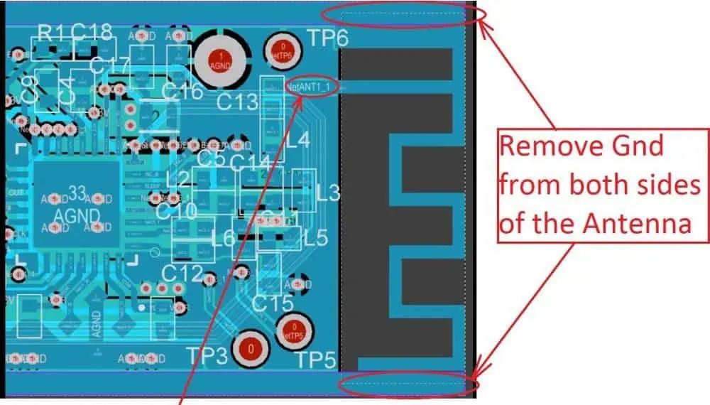
Minimize use of vias: To minimize the loss in an S-matrix of interconnect, it’s advisable to reduce the number of vias and avoid unnecessary layer transitions. Additionally, the remaining vias can act as antennas and generate strong radiation. You can find more information about this topic in our article.
When working with a particular frequency range on your board, It’s a good idea to think about routing through a layer inside the circuit board between the plane layers. It is important to ensure that the vias have the proper size & space from the planes to accommodate your working frequency. However, this task is challenging and cannot be easily calculated. Therefore, we advise examining this point through measurements, such as S-parameters. When a signal goes through the via into the interior layers of the circuit board, the impedance of the via is affectable by nearby planes and other conductors.
Designing an analog printed circuit board layout requires careful consideration. Still, by utilizing appropriate design tools & rules-driven software, you can implement the design principles for all digital circuits to maintain a noise-free analog circuit system and ensure signal and power quality.
Altium Designer® offers the best features for PCB layout. Whether for analog, mixed-signal, or digital PCBs, all within a single layout environment. It includes powerful routing equipment that can enhance your productivity.
The objective of the guidelines presented here is to prevent interference in analog boards that either comprise a digital segment or multiple analog signals with various frequencies by facilitating efficient routing & placement.
1. Keep Consistent Ground Potential
Achieving a consistent ground potential across the entire system is the primary rule for creating analog PCBs. Typically, this involves connecting ground nets in the system, ensuring that any voltage steps taken at one area of the printed circuit board will yield the same result as that taken at any other area.
When dealing with digital and analog signal interfaces, we recommend employing a continuous ground layer for both kinds of signals. It is advisable not to divide the ground plane into separate sections and attempt to route different signals between them, as this could result in large/non-existent return paths. Such a setup could lead to an EMI (Electromagnetic Interference) issue through the given mechanisms:
· A floating ground area could cause significant radiation, leading to a failure in emissions testing.
The person creating the design can put the path of the circuit over gaps in the ground parts, and this might create waves that go out.
Ground offsets across signal couplings trailing ground splits may cause incorrect voltage readings.
2. Comprehend Placement & Return Paths
Another crucial aspect to consider is the placement of elements in analog circuits. Similar to digital components, components in analog circuits should be positioned above the ground layer. Additionally, the location of the components will play a significant role in determining how signals interact through coupling.
To avoid signal interference and ensure that the return path of the current does not mix, it is advisable to place analog and digital signals in separate areas of the printed circuit board. So, If working with many analog signals, attempt to separate them perpendicularly. Similarly, when the printed circuit board has many analog interfaces & components working at various frequencies, employing an analog-digital separation approach could be beneficial.
3. Know to Place & Route ADCs/DACs
It is crucial to recognize the significance of ADCs & DACs in systems that combine digital & analog domains instead of delineating a ground plane split as a boundary between them. ADCs & DACs are key elements where the analog and digital worlds converge. It is essential to adhere to specific power & signal needs in ADCs & DACs, such as:
We don’t recommend employing separate analog & digital grounds. Instead, connect the DGND & AGND pins on one plane.
It is also not advisable to use a ferrite bead for isolating the digital and analog input pins unless you don’t confirm its efficiency via experiments or simulations.
If the ferrite isn’t deemed suitable in the scenario mentioned above, it may be necessary to employ two separate power supplies for the digital and analog power inputs.
It may be beneficial to implement charge compensation at an analog input to avoid transmitting noise into the ADC or DAC.
It is essential to comprehend how to choose and position voltage references that can endure power droop, noise, and temperature drift.
4. Apprehend Power Transfer & Impedance Matching
Inputs on a digital circuit in digital systems have more impedance, equal to a shunt impedance, causing them to reflect strongly. Consequently, speedy buffers are typically used to finalize the signal to ensure that an input capacitance at a receiver is original, thereby preventing reflection at a receiver.
In an analog system, signals can reflect at the receiving element as all signals demonstrate wave propagation by traversing an interconnect on a PCB. Nonetheless, one should note that not every analog system necessitates the reception of the signal at very high impedance(capacitance) input. In certain instances, you can use these signals to drive the moderate or low impedance input, which may possess some reactance. In such scenarios, the objective could be to provide power, voltage, or current at a certain frequency.
The primary focus here is on comprehending the design of capacitance-matching circuits and incorporating capacitance matching in a printed circuit board layout. The objective is to achieve conjugate impedance matching, which involves using an impedance (capacitance) transformer with the stub lines.
5. Identify the Need for Shielding
One common approach to address noise problems in analog systems is to add shielding to the affected nets. However, it’s important to carefully consider the best method for achieving effective shielding. It could involve stitching through holes, applying a shielding element, and utilizing a custom-shielded gasket. The choice of shielding method will depend on the specific requirements of the system and the type of noise being addressed.
Analog integrated circuit design generally follows the top-down layout and implementation procedure, followed by the bottom-up process. However, there are numerous variations in this approach. The following are the fundamental steps:
Create a high-level design specification that outlines the intended functions of the design and sets targets for its performance, power consumption, and cost (i.e., area).
Create a high-level design plan that can meet the desired specifications by utilizing macro functions like amplifiers, comparators, and filters.
The next step involves creating device-level descriptions that support a top-level layout using capacitors, resistors, and transistors. One can do it by drawing from the library of already defined functions.
Verify the designer’s ability to meet all its requirements by performing simulations. So the tool used for this step usually involves modeling the board using non-linear and linear components optimized for the specific fabrication process. It is where one evaluates the device’s robustness in the face of the manufacturing process & operational variability.
Assemble pre-defined designs of all elements to implement a physical design layout. During this step, one can perform the optimization of the design density to minimize price. Adherence to placement rules is crucial to ensure the layout is designed for signal integrity and manufacturability. This step, known as physical verification, validates compliance with these rules.
The next step involves extracting the equivalent board from the physical layout. This process considers parasitic effects, including crosstalk & wiring resistance. They were not present in a circuit model useful for simulation. The extracted circuit is then re-simulated to verify the design meets its performance targets with the added parasitic effects. Additionally, the extracted design is compared to the original layout. It is to ensure that the correct applications were used & connected as intended. This process is LVS checking.
In this step, they add things to test the circuit. After this, the design is ready for a bigger digital design. When you add an analog design to a bigger digital design, it’s called AMS/analog signal design.
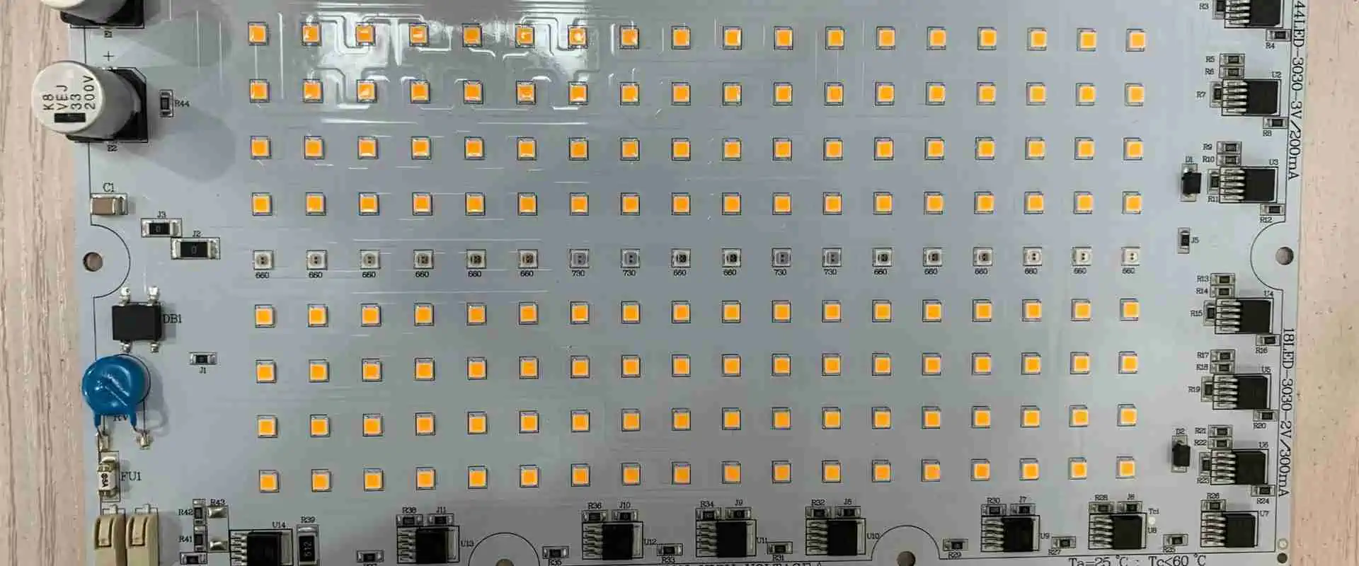
Affordable and durable lighting sources are the preferred option for modern commercial and residential lighting systems. LED lighting is the top choice for applications such as automotive, housing, & outdoor lighting due to its high output lumens & efficiency. To enhance their functionality, PCBs have LEDs mounted with an integrated power circuit. LED circuit designs differ from other circuit board designs because they tend to generate excess heat. To counteract this issue, LED printed circuit board designs utilize aluminum printed circuit board substances, heat sinks & structural substances to dissipate thermal power from the board. This article will explore the challenges, types, and considerations of LED printed circuit board design.
Why Use LED PCB Circuit Design?
LED illumination systems rely on LED PCBs as their foundation, which offer numerous advantages as light sources, including:
Compact size: The small size of Light-Emitting Diodes makes them well-suited for various applications, including but not limited to computers, automobiles, smartphones, floodlights & traffic lights.
Lower power consumption: LED lighting is the preferred choice for residential lighting due to its energy-saving properties. By using LED lights, power consumption can be reduced by approximately 80%
Longer lifespan: Compared to traditional light sources, LEDs have a lifespan that is 25 times longer.
Mercury-free: A traditional bulb has a significant environmental impact because they contain mercury, which necessitates special disposal ways. In contrast, LEDs are mercury-free and can be easily positioned, resulting in less pollution than traditional lights.
Efficiency: LED lights generate less heat than incandescent lights. It is because the energy used by LED (Light-emitting Diode) lights is primarily used for lighting instead of heating.
Around 90 percent of the energy consumed by traditional bulbs is emitted as heat, whereas for LEDs, heat distortion accounts for approximately 20% of their total energy usage. Nevertheless, generating even 20 percent heat can pose a significant risk to LED circuits, and several challenges must be tackled in the design of LED PCBs.
The design of LED PCBs must tackle the following problems that LED(Light emitting diode) lighting systems encounter.
Temperature: Insufficient thermal management in LED PCBs can cause a rise in board temperature due to heat generation, which can significantly affect the longevity and color of the LEDs.
Lifespan: Although LEDs are renowned for their extended lifespan, elevated temperatures in LED(Light emitting diode) circuits can diminish their longevity.
Color of LED light: LEDs are utilized in various applications to produce specific colors, but when the temperature rises, it can result in color discrepancies in the LED illumination.
Effective thermal management is a crucial issue that must be tackled in LED printed circuit board design. To guarantee optimal efficiency, prolonged lifespan, and vivid LED illumination, precise temperature regulation is essential, particularly in critical LED applications.
Considerations for LED PCB Circuit Design
Several LED printed circuit board design factors require top priority consideration.
Cost vs. quality: The design of LED printed circuit board boards involves considerations of both cost & quality, which are closely related. Factors such as the placement of LED components, thermal management capabilities, coupling effects & overall performance are crucial in evaluating the LED PCB quality.
A numberof layers: An LED printed circuit board can have a double-sided, single-sided/ multilayered design, with no. of layers determined by the specific application requirements.
The popularity of LED PCBs among engineers & designers tasked with product upgrades or revisions can be attributed to several reasons.
Generates light with minimal heat production
Enables easy sourcing and assembly of products due to the layout of LED( Light emitting diode) membrane switches
Exhibits strong resistance to moisture & dust impacts.
The product boasts low & efficient power consumption, resulting in energy savings.
It comes in a range of sizes, intensities, and colors, providing ample options for selection.
The product can be seamlessly integrated into complex assemblies of interface with ease.
Being lightweight, it can be effortlessly transported from one place to another.
The product has high stability and a low profile.
LED printed circuit board design provides a cost-effective option for backlighting icons and symbols.
LED printed circuit board design has an extended lifespan, resulting in savings on maintenance & replacement costs.
Like other PCBs, a backlit LED printed circuit board design is a more affordable choice.
LED printed circuit board design is compatible with copper and silver flex membranes.
The LED printed circuit board design provides ample flexibility, even in more complex assemblies.
Where to use LED PCB Circuit Design?
· LED Strip PCB Design
A PCB with SMD Light Emitting Diodes mounted on its surface, which can be either flexible/rigid, is commonly known as an LED strip. The layout of an LED strip PCB must take into account various critical factors such as water resistance, as well as current and voltage considerations. The color variation and if the Light Emitting Diode is addressable are also significant factors that impact the design.
Several options are available for LED strip printed circuit board design, including uni-color non-configurable, flexible white non-configurable, multicolor non-configurable, & RGB addressable. These options have various uses in appliances like decorative lighting, fluorescent lighting, and even in the production process for UV inspections. Therefore, proper LED strip PCB design is crucial for achieving the desired outcome in these applications.
· SMD LED PCB Design
SMT LEDs apply in various electric equipment, such as notebooks, network systems & cellular phones. Similar to other LED printed circuit board designs, these PCBs offer exceptional heat dissipation capabilities.
· LED Street Light PCB
LED Street light PCBs are specifically engineered for street lighting purposes, incorporating VMS technology that proves beneficial for traffic guidance systems. Besides, LED lighting ensures consistent luminance, contributing to enhanced visibility during the night and facilitating traffic management. Consequently, these printed circuit boards are made to ensure optimal street illumination and seamless communication (signalization).
· PCB Design for LED Bulb
LED PCBs are widely utilized for producing LED bulbs, making them one of the most popular applications of this technology. This technology is the driving force behind most bulbs available today.
Moreover, the design of LED PCBs for bulbs is also implemented in various other LED( Light Emitting Diode) light products, such as LED( Light Emitting Diode) panel lights & LED( Light Emitting Diode) floor lights. It is instrumental in achieving LED( Light Emitting Diode) ceiling lights as well.
It is a dot matrix display that can showcase a vast amount of information, albeit with low resolution. This type of display consists of a 2-dimensional array of diodes, with cathodes arranged in rows and anodes arranged in columns. Moreover, the printed circuit boards (PCBs) used in LED matrix appliances are designed to have a life of more than 50,000 hours, ensuring their longevity.
LED matrix displays have multiple applications, ranging from displaying animated images and information on enterprise premises to use in television, computer monitors, headsets, and medical monitors. They come in various types, such as 88 dot matrix, 12816 dot matrix, and others. These displays facilitate easy control of color and brightness.
· COB LED PCB Board
An array of diodes is through direct contact between multiple bare diodes and an MCPCB substrate, forming Chip on Board (COB). COB MCPCBs exhibit exceptional thermal conductivity, facilitating perfect heat distortion.
COB MC printed circuit boards offer a simple LED assembly & can reduce space consumption while being relatively inexpensive. They find various applications, such as backlighting for Light Emitting Diode TVs, street & parking lighting, car lighting, horticulture lighting, and high-energy LED applications.
Other PCB Design for LED Light Systems
LED PCBs have a range of lighting applications, each with unique design characteristics. For instance, LED lighting printed circuit boards in the telecommunication sector prioritize low weight & noise resistance.
LED equipment in telecommunications generates significant amounts of heat, and here the superior heat dissipation property of aluminum-based materials proves valuable. These PCBs find application in high-speed equipment such as filter circuits.
How to Choose LED PCB Circuit Design Material?
· Fire Retardant
The chosen material must possess fire-resistant properties capable of slowing down or halting the fire spread during an outbreak. It is through the chemical reactions that render fuels minimally flammable and prolongs the combustion phase, thus averting the risk of the LED circuit board caught fire.
· Dielectric Constant
It’s important to take into account the electrical power storage capabilities of the material. Additionally, the electrical force strength from the dielectric constant, making it a crucial factor to consider. Keep in mind that LED circuit boards use in electrical appliances, so make sure to evaluate the material’s electrical power storage capability.
· Loss Factor
A substrate substance serves the function of dielectric loss, which the dissipation factor can measure to determine performance differences between materials. A lower dissipation factor indicates less dielectric loss in the laminate. It’s important to select a laminate material with a lower dielectric loss for use in the substrate.
· Tensile Strength
Tensile strength refers to a substance’s ability to resist breaking under tension or the maximum load it can sustain. It indicates that the material can withstand stretching without breaking. Ensure the LED printed circuit board materialhas the necessary tensile strength.
· Glass Transition Temperature (Tg)
When considering the use of polymers, it’s essential to consider their Tg. At this temperature, the properties of plastic transition to a crystalline state. Above this temperature, the same substance becomes rubbery. This property is crucial to consider when using polymers for end use.
When designing the LED printed circuit board, it’s important to select a material with a sufficiently high Tg to ensure that the board can perform well even under harsh temperature conditions.
· Z-axis Expansion Coefficient
Dimensional stability of an object refers to its changes in size when subjected to varying temperatures, also called thermal expansion. Determine the coefficient of thermal expansion under constant pressure. Different ways for measuring the expansion, including volumetric, area, and linear methods.
To avoid creating weak solder joints, it’s important to ensure that vias are not positioned too closely to SMT pads, especially when not masked. Maintain a minimum distance of 0.025″ between the edge of the via & SMT trade. Additionally, it’s advisable to apply a mask via a pad.
· Avoid Routing Wide Traces
It is recommended that the width of the surface mount pads be greater than that of the traces that connect to them. If the traces extend beyond the pads, the amount of surface area available for the solder finish will be limited by the size of the solder mask opening. It can result in insufficient coverage by the solder paste, as well as diminished heat dissipation. To ensure proper coverage and heat sinking, the surface finish area determine the size of the pad rather than the size of the trace.
· Designing Sides of SMT Pads
To prevent potential issues, it is advisable to refrain from routing along the edges of surface-mount technology (SMT) pads. Instead, the traces should be routed to connect with the pads at a midpoint along the edge. When there is a gap between the trace & pad etchant can become trapped and corrode the trace during the rinse cycle. Additionally, such connections are prone to failure due to thermal shock during assembly and may even result in oversized pads. We advise to review and amend any trace routing for these connections as necessary.
· Don’t Route Circuit Trace at an Acute Angle
Routing at acute angles, which are less than 90 degrees, can lead to issues that may fail. Acute angles tend to concentrate stress, harming the system’s integrity. To mitigate this issue, we advise to reroute corners in a manner that results in angles mohan 90 degrees. It can help to distribute stress more evenly, reducing the likelihood of failure.
· Don’t Place Components Too Close to the Board’s Outline
Positioning elements too near the size of the PCB can be risky, as they may get damaged during a de-penalization process. It is advisable to keep SMT components at least a hundred inches away from the board’s edge to prevent any potential damage.
To ensure the safe placement of components during PCB design, it is recommended to include a tab location. It can help you determine if the element is properly positioned or if adjustments are necessary to avoid any potential damage during the de-penalization process.
· Don’t Export Gerber files at 2:3 Decimal.
The 2:3 ratio, a popular method for transferring files onto floppy disks, is unsuitable for more compact designs. This approach often results in the loss of crucial data and can cause issues with arc points.
· Consistency in Solder Mask Openings
To minimize issues with design rules and streamline the manufacturing process of your printed circuit board (PCB), it’s important to apply consistent oversizing to your pad stack definitions for all components. It will help prevent potential flaws and simplify the PCB production process.
· Use Direct Connects for Vias
Merely addressing the circuit problems is insufficient; it is also crucial to guarantee the effective operation of the holes. Incorporating thermal pads in vias, particularly crowded ones, may result in an open circuit situation. It is advisable to omit these features since they are unnecessary during manufacturing and can cause issues.
· Thermal Pad Sizing
Ensuring the accurate size of the thermal pad in the element hole is also essential. Congested pads in element holes can result in an open circuit. Thus, the interior diameter should match that of the exterior layer pads to avoid any issues.
· On the Through Holes
To maintain accuracy, the distance between a plated through hole (PTH) and the trace must be a minimum of 0.006″, particularly for multilayer printed circuit boards. Several factors impact the precision of this space in multilayer PCBs, such as:
Defects of LED PCB Circuit Design and How to overcome?
led bulb circuit board
When working with LED printed circuit boards, you may come across various defects that can affect their efficiency. While some of these issues are specific to LED PCBs, others can also be found in others. It is crucial to address these problems comprehensively and effectively to maintain the functionality of your LED PCB. In this article, I will guide you to some most common defects and provide solutions for overcoming them.
· Circuit Scratch
When the pads on a circuit board are together, it can result in recessive defects by scratching. This defect can expose the underlying copper, which can have serious consequences. To prevent this, we advise adding more copper foil to the circuit board to minimize the occurrence of open and short circuits. It can help to reduce the amount of scrap and improve the overall quality of the circuit board.
Defects exposed to copper may not always be noticeable until after the surface-mount technology (SMT) process. One solution to this issue is to reduce the line & pad pitch, which can cause the shrinking of the pitch. It can help to mitigate circuit scratching and lead to an overall improvement in the quality of the circuit board.
· Solder Mask Oil Peeling
If you choose to use the solder mask in your LED printed circuit board design, you must apply a significant amount of exposure energy. Additionally, using a thicker oil than usual can make it challenging to ensure that the oil at the lower layer is adequately exposed, resulting in the peeling of the (oil)solder mask. To overcome this issue, we advise applying exposure energy. However, when doing so, it’s important to consider the consignment ability of a solder mask to ensure optimal results.
· Bad Board Outline
A frequent occurrence during the application of Light Emitting Diode through-holes in smaller-sized boards without margins is the bulging of the board outline. Loose screws can lead to this effect, as well as board displacement during the process. To overcome this issue, we advise establishing appropriate margins that aid in the marking-up process. By doing so, the defect can be resolved.
· Solder Mask Oil Color Unconformity
It is a prevalent flaw with PCB, particularly in the LED sector of an LED circuit board. It is difficult to measure and meet the appropriate standards due to the lack of widely accepted standards for this issue. Numerous factors affect the conformity of oil color.
Attaining oil conformity requires adherence to stricter manufacturing standards compared to regular circuit boards. The best approach to achieve this is to explore suitable manufacturing ways and control parameters. However, this can only be achievable through years of experience in production and using new technologies.
· Board Angle Defects
When dealing with circuit boards with a relatively high thickness, it’s crucial to be mindful of the fragility of sides( angles). Board angle problems are likely to occur while transporting printed circuit boards. To prevent such defects, it’s essential to handle the delicate side angles of LED printed circuit boards with utmost care.
Moreover, it’s advisable to make the base plates relatively larger than standard single-margin printed circuit boards.
· Warpage
Typically, the warping of a LED PCB is caused by an uneven distribution of stress on the board, mainly due to multiple dense pads on a Light Emitting Diode side of a circuit board. The arrangement of large copper blocks on the driver side of the circuit board can also contribute to this issue.
One effective solution to this problem is maintaining a warpage of less than 0.5 percent, which assists in keeping the board flat and stable.
The intricate arrangement of pads often leads to omissions during inspection due to the strain & fatigue it causes. As a result, long inspection times and a low pass rate are common problems of arrangement.
It is essential to address pad outline issues. It’s important to define favorable production procedures to minimize the omission ratio and overcome these issues. Additionally, it’s worth noting that visual fatigue can significantly affect the performance of visual inspectors.
· Degrading Functions
You may have already observed that LED PCBs differ technically from other types of PCB. LED Printed Circuit Boards typically feature dense pads & black solder masks, which can present challenges during error analysis in PCB assembly. The dense pads and black masks can make it difficult to identify any malfunctioning LEDs accurately.
When a PCB experiences a function failure, the PCBA typically only indicates the failure without specifying which pad is at fault. The failure is an issue with a whole row of Light Emitting Diodes. If you encounter this issue, it may be necessary to take extra steps to discover the problem. Pinpointing the specific Light Emitting Diode causing the issue may require removing components and solder oil through demolition.
Conclusion
LED PCBs have a significant impact on our daily lives in numerous ways. By following this article, you will know how to create your LED Printed circuit board design and have a comprehensive understanding of the assembly & fabrication processes involved. Based on our discussion, you can select the best LED PCB option for your application. Overall, this guide has equipped you to handle any matters related to LED PCBs confidently.
According to IPC-TM-650 Protocol 2.4.24.6, Decomposition Temperature or Td is the heating temperature where a PCB substance chemically decays or decomposes. The substance loses a minimum of 5% of its mass weight. Td is measured in degrees Celsius (°C), much as Tg. The material’s capacity to withstand heat is determined by this characteristic.
TD Materials Test Method Manual
IPC-TM-650 Laminate Material Decomposition Temperature. This testing method outlines a process for figuring out the heat deposition of substrate laminate through TGA or thermogravimetric analysis. This testing method may not produce comparable findings when used on PCBs or even other composite materials.
We must first generate test samples for this test procedure. The sample can be either an unclad laminated substance (CCL) or a laminate substance with all of the copper removed that’s been roughly square-cut (using just water cooling/cleaning, no oil) to slide further into the TGA sampling pan. Sample mass (weight) typically ranges from 10 mg-30 mg. Samples must be trimmed to the required size using the right techniques and tools to reduce thermal shock and physical stress. Samples having a lesser surface area and the same mass can lose mass more slowly.
By an analogous or sanding procedure, all sample edges must be polished smooth and free of burrs. This allows the testing sample to rest entirely flat or straight over the sampling pan. Be careful not to subject the sample to excessive heat or mechanical stress. The mass readings must be accurate to within +/-0.01 mg.
The following components must be included in an analysis of the thermogravimetric or TGA instrument:
Null type microbalance with 0.001 mg sensitivity
Dry (dew point below -68°C [-90°F]), moisture below 3.5 ppm, and nitrogen (below 20 ppm o) purge are available on the furnace.
A temperature controller with a regulated 10°C+/-0.1°C [18°F+/-0.18°F] per min warming rate up to 800°C [1472°F]
The TGA must be able to accurately measure mass to the nearest 0.01 mg.
Test Procedure
Before testing, the samples of the test must be baked for almost 24 hrs at 110°C+/-2°C [230.0°F+/-3.6°F] and then cooled to room temperature. The TGA analysis should begin within 15 min of withdrawing the sample from desiccators in a conventional lab setting since samples may develop mass as a result of moisture content.
Set the balance’s accuracy to +/-0.01 mg.
Adjust the sensor’s calibration of temperature to within +/-1.0°C (1.8°F).
The purging rate should be set at 55cc/min (0.9mL/s). Thirty minutes should pass after the TGA air purging before introducing a sample. The calibration of the instrument will be significantly impacted by the rate at which the gas flows through the cell. As a result, the instrument should be calibrated using the same rate of flow as that utilized during the test. Positioning the digital thermometer should prevent it from coming into touch with the flow rate that will be utilized for the test. It is important to place the digital thermometer such that it never makes contact with any sample. The device may be calibrated once the thermometer has been placed properly. Following this, neither the flow rate nor the sensor placement should be altered.
Measure the sample’s mass after placing it into the TGA.
The sample should be heated at a temperature of 10°C/min from ambiance (no higher than 50°C) to 550°C.
Keep the temperature’s track, Td (2%), where the sample weighs 2.0% which is lesser than it did when it was recorded at 50°C.
Keep the temperature’s track, Td (5%), when the sample weighs 5.0% which is lower than it did when it was recorded at 50°C.
Monitoring PCB temperature is essential because it can prevent failure, as high temperatures can alter a PCB’s function and structure.
Tracking the temperature of PCB is particularly crucial since the consequences of excess heat don’t have to stay isolated. They have the potential to spread quickly across specific PCB components. This leads to numerous mistakes and damages. Overheating a PCB can lead to the following types of damage:
· Loss of Structural Integrity
Extreme heat can compromise the integrity of a PCB. When it becomes too hot or cold, layers of PCBs shrink and expand. This is because they are extremely delicate to temperature variations. High temperatures can induce warping in the widths, lengths, and thicknesses of some PCB layers.
· Disruption of Circuit Line
Excessive heat can potentially harm electrical circuits. Circuit wires expand and acquire new forms when they get too hot. When this happens, the circuits may be affected by distortions, frequency shifts, and direct losses. Its conducting impedance, which really is ordinarily 50 ohms, may also change. Microwave and millimeter-wave PCBs are susceptible to harm when tiny, delicate components expand or bend at high temperatures.
· Expansion Rate
Various substances stretch at varying speeds, exacerbating the previously listed detrimental impacts. The two most common layer types on a Circuit board are conductive metallic and dielectric layers. Because they are made up of different components, they react to heat in a different way and expand in diverse ways.
As a result, an overheated PCB may experience more harm and absorption of moisture when the different sorts of layers split.
· Oxidation
Concern exists over PCB electrical components oxidizing over high glass stream temperatures. Exposed dialectic substances used in PCBs are not shielded from oxidation if a protective laminate layer is not there. In that case, the material may corrode after being subjected to extreme heat. Increased dissipation is typically the result of transmission line breakdown.
When an electric component fails and eventually dissipates, it is another common cause of excessive temperature in the PCB, as it does not produce the needed amount of power. The nearby components must provide additional power to compensate for this. Creating more electricity raises concerns about overheating.
· Interference Through-Hole
Through-hole and heat-sink electrical components make up the power-supplying components of PCB. They generate heat and radiate it into space. In order to compensate for incorrectly soldered through-hole or heat sinks interference from some other PCB component. However, the other components will generate considerably more heat than usual. In this situation, there is also a risk of overheating.
· SMD Distance
Surface-mount applications connect to the PCB in a similar way as through-hole electrical components. Through-hole and heat-sink components enable a more organized current flow from them. Through-hole and SMD components, however, must be appropriately separated from one another.
If they are too far away, this current must move farther. Because of the longer time needed for the current to travel, certain receiving electrical components may get too hot. Thus, other components can begin to overheat.
· High-Frequency
Compared to other applications, high-frequency PCB devices are more likely to face high temperatures. The reason is that greater heat will definitely come from increasing power output.
For instance, a rapidly growing field of PCB development is radio-frequency circuitry. Despite their intricacy, these circuits have a variety of real-world applications. This includes wireless security in medical and industrial equipment as well as smartphones. These Boards demand special design techniques, as high-frequency PCB can produce an excess amount of heat.
· Solder – Lead-Free
The PCB sector is changing in order to reduce dangerous elements. RoHS PCBs employ solder free from lead. This requires high temperatures to flow freely.
Did you ever lose track of the wedding ring? We certainly did because we often took it off during gym. When we finally realized we couldn’t remember where we had put it, frightening thoughts of what we might find at home flooded our mind. However, after nearly hours of searching, we discovered the ring was in the same condition.
Misplacing the wedding ring is a significant concern, but encountering problems with annular rings on a printed circuit board (PCB) can be just as problematic. When there are issues with annular rings, it can break the flow of the electrical path and affect how well the circuit works as a whole.
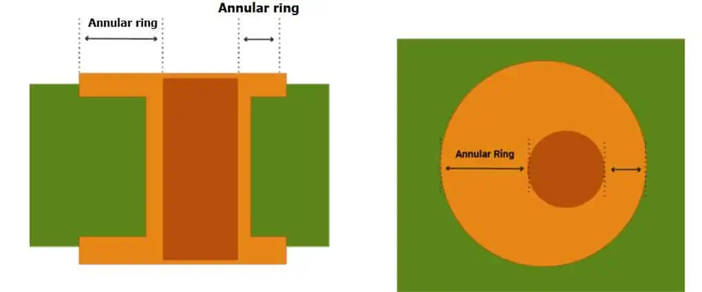
What Is An Annular Ring Via?
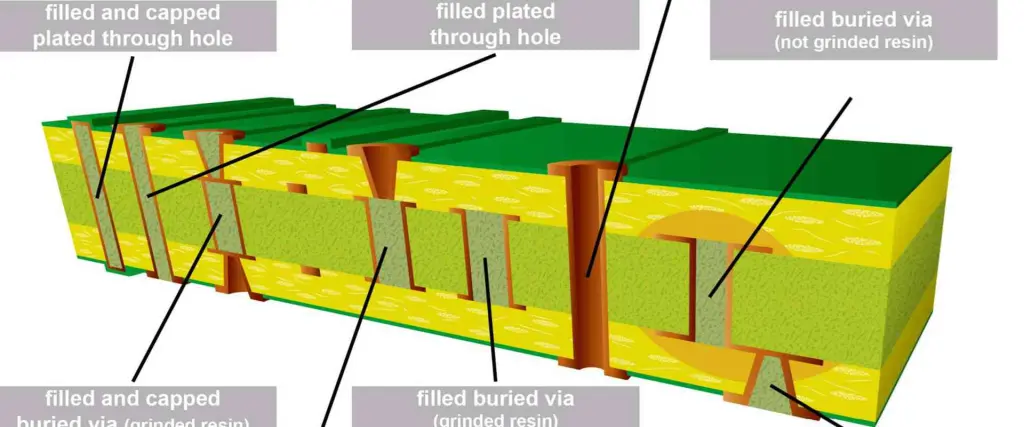
The technical term used to describe the region between the drilled hole of a via & the border of the copper pad is an annular ring. Vias act as connection points linking various layers on the printed circuit board.
It is necessary to know about the construction of a via to comprehend the fundamentals of annular rings. When a PCB is manufactured, the process involves etching the board, leaving via pads aligned on various layers. Subsequently, the pad is drilled to create a hole, where copper is precipitated through electroplating.
Upon observing the printed circuit board from above, the drilled through-holes present themselves as circular-shaped patterns referred to as annular rings. These rings can vary in size, with some PCB designers choosing thicker rings while others may opt for thinner ones due to spatial limitations.
Although vias are an integral component of printed circuit board manufacturing, it is a fallacy to presume that annular rings are infallible. Misshapen annular rings can arise, which may impede trace continuity.
Theoretically, the ideal circular ring is achieved by drilling precisely at the via pad. However, in practice, the accuracy of drilling hinges on a machine used by the printed circuit board manufacturer. These manufacturers have a particular tolerance for annular rings, typically around five miles. In simpler terms, there exists a likelihood of drilling being slightly off-target within the designated limit.
In the event of a missed target during drilling, the ending hole may shift towards the side of a pad, leading to tangency between the hole and the pad. Should the drilling stray even further from the mark, a breakout will occur. A breakout condition arises when a hole part surpasses the designated pad area.
Annular breakout can impede the via continuity, reducing the copper area linking the hole & pad, thereby affecting the current flow. This issue is more noticeable when the affected area channels a significant amount of current. To address the problem of the annular breakout, the exposed area is typically remedied by adding more copper padding, a process known as tear-dropping.
There are certain scenarios where an annular breakout can lead to irreparable issues. For instance, if a hole deviates to the extent that it pierces an adjacent trace, an unintentional short circuit may occur on the printed circuit board. This problem is challenging to resolve as it necessitates isolating the shortened trace & via.
Getting The Annular Ring Via Size Right
Although PCB manufacturers are responsible for creating precise annular rings, designers can contribute by selecting the appropriate size for a layout. It is advisable to allocate extra space beyond the manufacturer’s tolerance level to ensure accuracy. A general thumb rule is to increase the size of the annular ring by 1 mil, which can prevent potential problems in the future.
How to Get the Annular Ring Via Size Right?
Every PCB manufacturer has a specified tolerance for an annular ring in the printed circuit board manufacturing process. Nevertheless, it is prudent to allocate more space to be cautious.
We advise to enlarge the 1.0mm size from the producer’s specifications. This minor increase in width can assist in avoiding any potential problems in the future.
The specific purpose of the PCB design influences the annular ring size. PCB institute has established three classifications for PCBs: Class 2, Class 1, & Class 3. PCBs designed for high-stress applications necessitate large annular rings to accommodate the wider diameter. Class 3 PCBs, in particular, demand heavier annular rings to withstand rigorous usage.
Certain PCBs accommodate large and heavy equipment, while others are essential to be highly compact. For instance, PCBs in small technological devices need to be extremely space-efficient.
In such scenarios, the annular ring size needs to be proportionally small. However, what is the smallest possible size that we can achieve?
There is a variation in the limit for outer and inner annular rings per the industry’s design standards.
In an annular ring, the minimum width on the inner side of a printed circuit board is 0.1mm.
In annular rings, the minimum width on the outer side of a printed circuit board is 0.05mm.
Difference Between a PCB Annular Ring Via and a Through-Hole
The term PCB often evokes thoughts of the via method, which involves mounting electronic components onto a printed circuit board. This technique entails inserting the components into drilled holes on the board.
Through-holes are created by inserting leads into drilled holes and then soldering them onto copper traces to establish conductivity.
In contrast, annular rings establish conductivity by linking the Plated through-hole to a copper trace.
Teardrop Annular Ring Via
A teardrop annular ring has a shape resembling a teardrop. Rather than being a circle, extra copper is there to connect the outer edges of the ring, providing it with additional strength.
Teardrop annular rings are primarily utilized when there is a risk of the drill head deviating from its intended path during drilling. So this issue can result in the removal of excess copper, which may compromise the connection.
Teardrop Annular Ring Via can:
· Minimize the hazard of cracks on thin copper
Alleviate thermal or mechanical stress
Take precautions to prevent small deviations in the positioning of a drill hole.
Best Designs of Annular Ring Via for Your PCB
Manufacturing processes generate annular rings, and as a result, the standards that oversee board construction also outline specifications for these rings. These standards include IPC-2221, a generic standard for printed board layout; IPC-A-600, which specifies acceptable standards for printed boards; and IPC-6012, which provides performance and qualification specifications for rigid printed circuit boards. The standards generally establish the minimum dimensions or the lowest tolerances based on the IPC categorization, which is determined by the intended use and location of your PCBA. By following these standards, a series of crucial steps can be generated to produce a board that meets regulatory compliance and is of high quality. These essential steps are:
Essential Steps for Annular Ring PCB Design
Identify the IPC of your board and familiarize yourself with the corresponding standards for its development.
Find out the necessary clearance specifications for the annular ring.
Then, find the minimum required width for the annular (circular) ring.
Moreover, find the minimum required thickness for the via (if it is applicable)
Choose the appropriate size and placement of the(circular) annular ring.
For optimal annular ring printed circuit board design, ensure your specifications comply with the contract manufacturer’s DFM guidelines and rules. Failure to do so may lead to issues such as breakout, solder expansion, or solder bridging.
In general, we advise that the diameter of your annular ring be at least as big as most force-exposed parts, such as a switch. The optimal diameter for an annular ring typically falls around 0.25mm. If you are uncertain about the size of your via, using this diameter as a fallback is a viable option.
The PCB manufacturer typically sets the minimum dimensions for vias and annular rings. It’s important to follow their specifications and ensure that your annular ring meets or exceeds the smallest size requirement. If the annular ring is smaller than its specified size, it could lead to inadequate connectivity for the components.
When contemplating the size of your drill, it is important to consider several factors, including the method of tenting, plugging, or filling your via, the amount of board space available, and your PCB’s current capacity. These are all critical considerations to make.
It’s advisable to check the copper traces and aim to make the diameter of the hole half of the copper lad’s area size. It can help ensure optimal results.
Wrap up!
If you’ve arrived at this part of the article, it indicates that you have a good grasp of the basics of the annular ring. We covered the definition of the annular ring and guided how to determine its dimensions. Besides we also delved into the connection between vias and annular rings and explained why their sizes are crucial. RayPCB trusts that you have found this guide informative and beneficial. Thanks for your interest!
The world of PCB manufacturing is extensive, encompassing a wide range of PCB types meticulously crafted to fulfill distinct functions. Since PCBs are the backbone of numerous electronic devices worldwide, their importance cannot be overstated.
Custom Arduino PCB – What is it?
The purpose of an Arduino printed circuit board is to facilitate the creation of electronic projects by including microcontrollers and an IDE. As an open software platform, Arduino is increasingly becoming a preferred choice among novice enthusiasts in the electronics field. An advantageous feature of the Arduino is its ability to load code onto the board without additional hardware, as this can be accomplished with a simple USB cable.
In addition, the IDE employed by Arduino utilizes a variant of C++, which significantly simplifies the learning of programming concepts. The common form factor an Arduino platform providesmakes the microcontroller readily available in a user-friendly package.
Arduino software & hardware are for individuals inclined to create interactive objects. This platform is highly suitable for artists, designers, and novices and supports communication with diverse devices such as the internet, LEDs & GPS units. Due to its user-friendly nature, the Arduino software and hardware are comparatively easier to grasp. As a result, numerous users have devised instructions for various projects on Arduino.
The Arduino finds its application in numerous fields, including robotics. Arduino circuit boards form the core of various electronics projects, making them an essential component in the field. Being a compact circuit board, the Arduino is an excellent choice for straightforward electronic projects. More projects can also be achievable by combining multiple Arduino boards.
If you’re fed up with using a breadboard to assemble your circuits and want to connect Personalised circuits to the Arduino, it’s time to consider creating a Personalised Arduino shield. These boards share the Interboard connection and form factor of your preferred Arduino base circuit board while allowing you to govern several fundamental aspects of your shield board’s layout. Furthermore, you can even create these circuit boards adaptable if you desire, akin to the shield circuit board demonstrated previously.
If you are new to designing your Arduino shield circuit board, you can use the step-by-step instructions provided below. Alternatively, if you are interested in creating a personalized shield and want to familiarize yourself with printed circuit design software, consider downloading CircuitMaker – a free and user-friendly platform. In this article & upcoming ones, we will present various tutorials on utilizing Arduino & shield boards. These tutorials will cover a range of topics, including application development.
Although it may seem obvious, it’s easy to neglect the initial step when beginning the design of the Arduino shield circuit board: obtaining the structural dimensions of the shield & connector pinouts. While it may be tempting to dive straight into the layout process and begin creating schematics, it’s essential to obtain the linking pinouts early on to place connections on the correct pins in the layout properly. After completing the schematic capture & preparing to Ingest the layout into the blank printed circuit board layout, it’s necessary to ensure that the circuit board dimensions are set to match the thickness of an Arduino base circuit board.
Arduino shields often come in different dimensions compared to the base circuit. Still, the crucial factor is ensuring the width is set to align with the necessary pins on the primary Arduino board. It’s ideal for covering the entire circuit board to ensure the shield’s stability when attached to a baseboard.
When you’re prepared to create the circuitry & diagrams for your circuit board, launch a circuit designer and begin incorporating your components. The most crucial components you’ll require are the Pin strips, which facilitate connecting your personalized Arduino shield and the Arduino board.
Pin Headers
Pin strips with a 2.54-millimeter pitch are typically useful for Arduino baseboards.
The pin header will act as an interface between the Arduino base board and your customized shield board. To choose the pin strip for the shield circuit board, you may opt for a male pin header with some pins on every side, enabling you to link pins with jumpers effortlessly. Another option is to use the downward-facing pin header displayed earlier, which connects to the board when the upward-facing holes accept axial element leads. With this version, you could stack another shield circuit board on top if desired.
After choosing the pin connector, it’s necessary to create or find schematic symbols that can be utilized for the pin header in the circuit designer. The symbol selected must correspond with the pinout of the Arduino board, and it’s important to monitor the side of the circuit board where each pin connecter will be positioned.
After identifying the base board and creating a layout plan, you can select the circuits & components to incorporate into the shield circuit board. Theoretically, any components can be added to the shield circuit board as they can be accommodated within the designated space. At my company, we have designed industrial shield circuits for Arduino that utilize relays and support 120-240 Alternating Current power, as well as simpler digital circuit boards with interfaces for multiple sensors. The potential for customization is boundless. A shield circuit board may incorporate various circuits and components, such as:
Power: Would an outer power source (AC,12 V DC, 24 V DC) be required for the board, or could the devices require power by the 5 Voltage pin? It may be necessary to incorporate a regulator, such as a switching converter or LDO.
Connectors:Screw connectors are a practical solution for establishing secure mechanical connections with outer wired devices. An alternative option is using pin strips on a shield circuit board to establish the connections.
LEDs, buttons, and switches: LEDs are highly functional for serving as indicator lights, whether to display logical states or to indicate the status of toggle switches. Such circuits can activate logic states on General Purpose Input/Output or the circuits of your shield circuit board.
Specialized ASICs: Numerous ASICs are available for diverse electrical operations. Integrating them into a personalized Arduino shield is a simple task as they typically establish a connection through SPI/I2C, and configuring them for your application is hassle-free.
To achieve a reconfigurable circuit board, you can incorporate a perf board with the hole array into your Arduino design. It emulates the functionality of a breadboard and grants you some degree of flexibility in the layout.
Custom Arduino PCB Perf Board Shields
Including a perf board part on the shield, the board provides a designated space where you solder personalized circuits featuring via components. These circuits can seamlessly interface with the other fixed boards on your shield board. Additionally, you can establish a connection between these circuits and the pin header, enabling them to directly link to the Microcontroller Unit on an Arduino base circuit board. The shield board contains a perf board section that facilitates the construction of customized circuits. You can utilize small-gauge jumpers to establish links between components in this section.
What makes these boards intriguing is their ability to be easily reconfigured by removing components while allowing them to connect to the pin headers using wires. To ensure that via components are easily soldered, it is important to use through-holes with proper-sized pads. As seen in the image above, the hole spacing is too close together to directly solder pads. Therefore, it is crucial to ensure that the holes are big or a rail is present to allow wires to be available between an element pin & hole.
Certain pre-packaged circuit boards come equipped with the ground plane. Similarly, you can incorporate this feature in your personalized Arduino shield. Doing so presents a chance to integrate functionality that typically requires an outer module, like Ethernet or wireless, into your design.
Shield boards are frequently utilized in the applications:
Ethernet: Although it may be challenging for a novice designer, it is possible to create an Ethernet shield by utilizing a controller IC with an integrated PHY & mag jack RJ-45 adapter. A mag jack is an essential component as it combines the magnetics & termination circuits within the adapter body.
Sensor interface: The Arduino-compatible boards come equipped with amplifier boards or ASICs to enable communication with specialized sensors. In addition to operational amplifiers in DIP packages, these interfaces will typically consist of surface mount device (SMD) components, such as ASICs. They usually utilize protocols like SPI, GPIOs, and I2C/ADC interfaces.
Wireless shield: These boards are designed to incorporate a wireless transceiver that utilizes a low-frequency protocol such as Zigbee, LoRa, or a BLE transceiver. The signals are typically directed into the transceiver controller through a bus module. To ensure signal integrity, it is recommended to follow the best practices for placing the ground plane or connecting the antenna.
Displays: OLED displays should be utilized on the shield circuit board. These displays can be connected over SPI using a shrouded adaptor. To create compact equipment with the display, it is recommended to attach the display to the shield board to ensure its stability and then direct the connections to a pin strip.
What Makes Up the Custom Arduino PCB?
The Arduino platform comprises several board variations, each designed for specific applications. Although these boards are for distinct uses, they share common components. Therefore, what are the components present on custom PCB boards for Arduino?
· Power LED Indicator
On the circuit board, there is a small LED that illuminates once the Arduino is with an energy source. If there is an issue, the light will not turn on. Therefore, if you do not see the LED illuminated, please double-check the board.
· Voltage regulator
It is a necessary element on an Arduino circuit board to regulate the voltage input. It acts as a gatekeeper by diverting excessive Electric potential from the board, which could potentially cause damage. Besides, it is important to note that this component has specific limits, and thus, it is advisable to avoid linking the Arduino to other devices exceeding 20 volts.
· USB/ Barrel Jack
Arduino PCBs require a power/energy source to function. The ATmega328P board can be powerable through a USB or by connecting a power supply to the barrel jack. Moreover, the USB linking fills code on an Arduino printed circuit board.
· Main IC
The IC serves as the central processing unit (CPU) of an Arduino printed circuit board, and its type may vary depending on the specific Arduino board. As a crucial component of the Arduino printed circuit board, it is essential to identify the kind of Integrated circuit that matches your board. This information is typically located on the upper side of an Integrated circuit. Additionally, the datasheets provide detailed data on the distinctions between various IC types.
· Pins
The Arduino board consists of multiple pins that facilitate wire connections. These pins have black plastic headers that allow wires to be plugged into the circuit. The Arduino printed circuit board includes various types of pins, which are labeled and perform distinct functions. For example, several Ground pins on an Arduino-printed circuit board help ground aboard.
· TX RX LEDs
RX and TX refer to receive and transmit, respectively and are markings commonly available on electronic devices to indicate pins for communication. In the case of the Arduino UNO, RX & TX markings appear in 2 distinct locations. Additionally, the LEDs on the RX & TX indicate when an Arduino is receiving or transmitting data.
· Crystal oscillator
The crystal oscillator enables the Arduino board to monitor time and generate communication signals & pulse thickness modulation. Additionally, the Arduino circuit can execute instructions at a rate of 16 MHz, which corresponds to the frequency of the Crystal resonator.
The Arduino encompasses various boards, each designed to fulfill unique functions. It’s essential to determine which board is appropriate for your task/work to ensure optimal performance.
· LilyPad Arduino
The creation of the LilyPad Arduino printed circuit board is creditable to Leah Buechley. This revolutionary technology combines electronics and textiles and features large connecting pads and a flat back. This flat back enables easy integration into fabrics using conductive thread. Moreover, the LilyPad family boasts a wide range of sensor circuit boards, as well as input, output, and power options.
· Arduino Leonard
The initial Arduino development board to feature an MCU with an integrated USB can handle USB communication directly. This board has software libraries that facilitate the emulation of various computer peripherals, including a keyboard, mouse, and more.
· Redboard
It is famous for its high reliability and user-friendly design. It can be easily programable using the Arduino Integrated Development Environment and a Mini-B USB cable. Additionally, the board is fully compatible with Windows eight without requiring any security setting changes. Incorporating a USB or FTDI chip enhances its stability, while the flat-back design simplifies embedding in various projects.
· Arduino Uno (R3)
It is a perfect option for beginners due to its user-friendly design. The Uno’s PCB is straightforward and includes all the necessary components to commence your project. With 14 input or output pins, the Uno board provides ample connectivity options. Moreover, the Uno features comprehensive support for the microcontroller, making it an ideal starting point for your projects.
· Arduino Mega (R3)
It is the same as the Uno version, boasting a significant increase in digital input/output pins. With the Mega, connecting to a computer is as easy as using a USB cord. Powering the board via battery is also possible, making it highly versatile for project development. The Mega is particularly advantageous for projects requiring multiple digital outputs/inputs.
Types of Pins on the Custom Arduino PCB
This board is equipable with numerous pins, each serving a distinct purpose.
· PWM
While these pins can operate as standard digital pins, they also can support advanced features such as PWM. Furthermore, the pins can imitate analog output, adding to the board’s versatility.
· Digital
It can function both as digital inputs and digital outputs, allowing them to power components such as LEDs and detect the state of other digital devices such as buttons.
· AREF
AREF stands for Analog Reference and enables the setting of an outer reference voltage ranging from 0 to 5 volts, which serves as the upper limit for analog pins.
· Analog
These pins are designed to detect and interpret signals from proportional sensors. For example, they can read heat sensors & translate their output into a readable value.
· 3.3v and 5v
This 3.3Volt pin supplies 3.3 power voltage; however, the 5 Voltpin provides 5. Most basic elements in Arduino are operational without requiring either 3.3/5 volts.
The Arduino printed circuit board is suitable for various applications, particularly communication between computers and devices. Arduino is a renowned company renowned for its expertise in both hardware and software development. So an Arduino Uno printed circuit board is a digital device to control equipment functions. Following are some examples of applications of the Arduino circuit board:
· Robotics
An Arduino board is a popular choice for robotics tasks, as it can supply the fundamental commands necessary for the robot’s operation. Additionally, the Arduino platform eliminates any potential interference from background programs, ensuring reliable and efficient robotic performance.
· Audio systems
Over time, there have been advancements in voice quality, and it has been a significant driver of innovation. Unfortunately, Arduinos cannot handle high-quality audio processing. Nevertheless, the Arduino printed circuit boards can still incorporate an audio component into your projects.
· Medical system
The medical sector has been witnessing continuous advancements, and one such example is the impact of 3D printing on this industry. While machines cannot replace the expertise of doctors, they can perform certain functions. In addition, some medical devices are equipable with Arduino software and hardware.
· Internet of Things
The growing popularity of the IoT is a significant trend. IoT refers to physical objects that can receive instructions online, allowing for completing tasks with minimal effort. Arduino is commonly popular in IoT projects.
· Arduino Programming Languages
The code for Arduino C++, a user-friendly programming language. The IDE is the text editor useful for programming Arduino. It assists in writing and uploading projects onto an Arduino printed circuit board. Additionally, there is a version of the IDE Arduino Website Editor, which allows users to store their projects in the cloud. The Arduino platform also supports its programming language, the Arduino language, and other web languages.
The IDE facilitates acquiring programming skills by providing an easy-to-use platform. Nevertheless, programming techniques can vary depending on the coding language utilized. Here are various coding languages that can be utilized with Arduino.
· Snap4Arduino
Snap4Arduino offers an excellent user experience to Arduino enthusiasts with its minimalistic user interface that prioritizes functionality over aesthetics. To install this program on your Arduino, you will require StandardFirmata. However, if you have already installed the Integrated Development Environment on your PC, the installation process should be straightforward.
· ArduBlock
Arduino is a beginner-friendly program that is accessible to anyone interested in programming. For individuals with limited experience, ArduBlock is an excellent tool that enables users to construct programs visually using a similar set of functions. This program is readily available for download and functions as a cover for an Arduino Integrated Development Environment.
Conclusion
Arduinos comprise numerous components and represent a software and hardware platform that supports the design and construction of various electronics projects. Compared to other microcontrollers, Arduinos offer a cost-effective solution. This article highlights the fundamental facts regarding Arduino boards.
The rate at which a PCB substrate expands when the material heats up is known as CTE or Coefficient of Thermo Expansion. Parts on each million or ppm expanded for each degree Celsius of heating is how CTE is stated. The CTE increases when the temperature of the material climbs past Tg. When a Circuit is heated, the substrate’s CTE, often significantly greater than copper, can lead to connectivity problems.
CTE is typically low in the axes of Y and X, ranging from 10-20 ppm for each degree Celsius. The reason for this is often because of the woven glass. It restricts the substrate in the directions of Y and X. The CTE also remains relatively constant as the temperature of the material rises over Tg. As a result, the material has to grow in the direction of Z. Aim for below 70 ppm/C for the CTE all along Z direction; when a material exceeds Tg, this value will rise.
All of the substrates in a Board have certain temperature-related material characteristics. The value of CTE, or the rate at which volume changes with temperature, is a significant thermomechanical characteristic of PCB composites. A designer must show concern about mechanical dependability since the system may flex excessively with high-temperature fluctuations.
A designer must choose materials to ensure that any CTE misfit among materials must minimize. It is to reduce potential mechanical issues which thermal excursions may cause. Although it will not be completely eliminated, the difference between CTE rates can be reduced to some degree. Continue reading to find out more regarding CTE values and the kinds of materials that fit better for thermal dependability.
All substances possess significant thermal characteristics often referred to as CTE or the thermal expansion Coefficient. This describes the rate at which a material’s volume will expand in response to a specific temperature change. It is commonly expressed in units of parts by million by degree. This means that the substance will contract or expand by 1/10,000th time for every time one °C rises. Temperature also affects other material characteristics like tensile strength and dielectric strength.
What Happens When There Is A CTE PCB Mismatch?
You want a PCB with high dependability when designing it. But a CTE disparity can lead to a number of reliability issues. Stress will develop and focus in the area between two unsuited materials as a result of variations in the value of CTE in PCB substrates. A single heat excursion seldom results in issues unless it is really severe. Yet, frequent heat cycling might result in volumetric expansion-related mechanical problems.
· Solder Fatigue
With high-reliability electrical devices that may endure extreme temperature or vibration variations, solder fatigue becomes a major problem. Solder fatigue happens due to the mismatch between the value of CTE of the substance or the copper for soldering. Vibration is another primary mechanical component causing solder fatigue. These two elements together can cause mechanical wear in welded joints.
· Solder Bridging
Changes in CTE mismatches and volume will have an impact on several PCB production processes. One issue that might occur while soldering BGA modules is solder bridging. Due to differences in CTE among various package materials, wire-bond-molded BGA components have a tendency to expand while reflow soldering at each corner. This results in the heated solder ball deforming, which may create bridging between neighboring balls, leading to a short circuit.
· Thermal Stress In High Aspect-Ratio Vias
The coating of copper along the walls of the via may become thinner when its aspect ratio gets higher. This makes the center extra susceptible to thermal or high-temperature stress cracking. As a result, thicker plating is needed to lessen the stress concentration during temperature changes on the board. Thermal cycling, or the repetitive change in temperature from low to high vv, is known for producing cracks via necks. Moreover, it leads to interfaces in layers in stacked buried-buried or blind-buried vias on HDI circuit cards.
· Delamination And PCB Warping
A significant temperature rise may produce enough stress which triggers layer delamination and starts the deformation of the PCB. Only if somehow the CTE discrepancy between the laminate and copper is too high. Circuit boards consisting of FR4 and copper are particularly prone to this kind of damage. This results from rapid temperature swings and CTE imbalance. Higher resin density laminates could have more CTE discrepancies with copper. Moreover, for a certain temperature change, thicker copper surfaces provide higher stress.
Be sure you utilize Cadence’ OrCAD to establish the design specifications. Generate your PCB design after choosing the components you have to construct a dependable PCBA. The greatest PCB layout and evaluation software comes with OrCAD. Users of OrCAD have access to a comprehensive collection of schematic tools, mixed-signal modifications in PSpice, and CAD tools.
If any of the components are susceptible to the extension of the Board, the x-y extension of the plane has detrimental effects. Components like large silicon packages or LBGAs, which extend at a rate of 6 ppm/°C while the Circuit board extends at a rate of 18 ppm/°C, can harm the board solder joints. After a significant number of thermal evaluation cycles, usually between -65°C and +125°C, the recurrent mismatch in expansions will result in shear pressures on the board solder joints. This, over time, creates stress and small cracking, and finally, work stiffening the solder with the breaking of the weld joint themselves. When it comes to demanding high dependability temperature circumstances like military weapons or medical equipment, the ensuing intermittent device operation is undesirable.
Extreme overheating (i.e., surpassing the temperature at which glass transitions, or Tg) across a series of heating sessions, like having numerous soldering cycles throughout the assembly, can also increase temperature variations. As an illustration, the pattern solders the Circuit with one thermally over the cycle and solders the chip with another thermal over the cycle. Then solder the big capacitors with a third thermal over the cycle. Limiting thermal cycles above Tg is crucial for the production and assembling of the Circuit since it has an impact on the total number of operational thermal cycles. According to tests, three thermal assembling cycles over Tg are equivalent to more than 1000 additional thermal cycles at 80 degrees Celsius.
A lower x-y value of CTE laminates is available that can limit PCB expansion and lessen the risk of weld joint breaking. The PCB can also be subjected to fewer thermal low-high temperature cycles and at a lower temperature by making better cooling and cabinet selections.
Thermal Stress Cracking In CTE PCB Assembly
Thermal stress fracture of the through copper plating occurs with repeated heat cycles. It is another area where the CTE of the Circuit board can impair the dependability of the Circuit assembly. PCB materials expand volumetrically as a result of temperature increases. However, because of the laminate architecture, the expansion of the x-y and z-axis behave quite differently. Since the laminate’s restraint glass fabric restricts the epoxy from extending isotropically (equally in all directions), the x- and y-axes will see much less expansion than the z-axis.
The high young’s modulus or the expansion force intensity of the tougher glass laminated inside the circuit layers of x-y regulates the epoxy volume expansion. This simply implies that because of the laminate’s slower expansion rate. The resin cannot move in the x-y direction and must expand in the direction of z. However, this will result in much more resin expansion in the unrestricted z-axis. This will put stress on the copper that has been plated on the vias.
Whenever the temperature gets near to a Tg, the z-axis CTE dramatically increases from 4 to 14 times the value of the x-y axis. This means that in a classic PCB laminate, the axis of z is expanding at Tg at a rate of 50-200 ppm/°C as opposed to 15 ppm/°C in the axis of x-y.
CTE is typically 16–18 ppm/°C for multilayer PCBs. The resin/fiber system with the lowest CTE of Circuit boards is likely to be the one with the highest resin concentration. It is feasible to create laminates with extremely low CTEs. Choosing prepregs and laminate carefully so they won’t suffer from epoxy famine. Starvation is indeed the absence of resin flow and incomplete filling of the copper pattern voids in the internal layer. Several laminate technologies manage the CTE of the z-axis, but only a few have been effective. The laminate systems that have been successful, like Kevlar, are highly costly and have limited availability.
For the majority of electronic equipment, including computers and televisions, a PCB or a Circuit board is a necessary component. This post will explain the fundamental structure and layout. As well as the assembly of a PCB and provide some pointers for building your own. Let’s get going!
You might want to check over some essential electrical principles. For instance, the fundamental circuits, electricity, voltage, connection fundamentals, or solder 101, on this World Electronics before we start.
Printed wiring chips and printed wiring boards are other names for PCBs. These labels are a throwback to the point-to-point cable wiring. When the insulator on the cables started to deteriorate and crack, there were regular short circuits and failures at wire connections.
The invention of wire wrapping has been advantageous for the more current boards. This method wraps a small gauge cable around each connecting point’s post. This actually results in a safe, sturdy, and yet conveniently changeable connection. Furthermore, a switch away from heavy vacuum tubes or retransmits to more compressed and reliable silicon and ICs resulted in a reduction in both the cost and size of components. A rise in demand for lightweight consumer electronics prompted developers to create increasingly more compact products to sell. Go to the PCB.
The “B” in the PCB refers to “board.” The stiff board comprises a network of wires and pads interconnecting. The purpose of the PCB is to make it possible to transport power and communications between actual physical objects. The use of solder aids this whole procedure. Solder is a metal (and powerful mechanical adhesive) that carries electrical links from the PCB surface to the components.
PCBs comprise various layers of different materials layered into one single object. Let’s split one right now, starting in the middle and moving outward from the surface.
The base or substrate of the Circuit board is where it all begins. The most popular substrate comprises FR4 and Fiberglass. This serves as the PCB’s support structure and lends it its thickness, heaviness, and stiffness. A more flexible type of PCB usually uses a high-temperature polymer like Kapton as a substrate.
PCBs come in a variety of forms and have been in use for many years. Circuits were connected on chasses, which were typically made of a metal structure and a wooden bottom before Circuit boards were invented. An Australian technician created a PCB as a component of the radio device in the 1930s, revolutionizing the field. Thankfully, since systems had to be powerable more effectively and everything had to get smaller. PCBs became more important not just in but of themselves. Moreover, owing to the Net, more linked to the rest of the world.
As a result, there have been breakthroughs in the construction of improved and compact PCBs. Furthermore, greater communication with more products that were previously out of reach, like wearable technology, smartphone apps, and a lot more.
How Does A Electrical PCB Work?
Whenever it concerns its structure, PCBs appear to be really straightforward. However, when it concerns the variety of things, they enable us to do with all of the modern marvels. No matter how basic a device may be, a Circuit board of some kind requires direct energy to pull into the gadget to serve its function. Really, it’s that simple.
Imagine being able to do little miracles. Miracles that were previously impossible with just some resin layers and a few solder channels enable electricity to flow through the various components of a PCB. PCBs support the mechanical aspects of the gadget in addition to channeling power.
This is due to the fact that PCBs direct electrical signals where they should go. Also, they offer a solid foundation for the components to all cling to. A brief glance at a PC and its internal components offers a great view.
Given all this assistance from a Circuit Board, it is easy to understand why PCBs are an item of equipment’s “brains.” Simply said, an electronic device wouldn’t function without any PCB.
Electrical PCB Like Never Before
In addition, PCBs appear to be quite straightforward. Their production involves despite the simplicity of their layout. It starts with a creator and includes the development of electronic layout automation (EDA) programs as well as production, assembling, and inspection.
This is the moment that a skilled circuit designer may truly be priceless. They are able to design a Circuit board that meets all of your unique technological requirements. Also, they’ll make sure you get the resources you require to succeed in your industry and prevent your PCBs from turning into your product’s weakest link. A very well PCB will make it simple to diagnose issues with your apparatus.
As a file containing the layout produces, the production starts right away. The real physical properties of the Circuit board identify and optimized throughout this procedure to produce a device with the fewest possible issues and the greatest possible advantages. Every output that produces needs a careful examination during this procedure to ensure that it performs well.
There is virtually no chance a PCB component will not go through testing with the test methods now available. This will guarantee that the PCB, which thus powers the product, won’t fail later.
MVI used to be adequate for identifying possible problems in electrical circuits, for instance, short circuits. Also, faulty solder connections, interrupted traces, a reversed component polarity, and lost components. Unfortunately, there were issues with the MVI approach, which was to errors by people while they carried out tedious and repeated tasks. This leads to cases where faults were either not discovered or were discovered at a late point in the design. This approach makes it prohibitively expensive to make changes to the circuitry.
The process of visual examination was then by utilizing the AOI method. Nowadays, AOI is a well-established inspection technique that is accessible on a number of pick-and-place equipment and is frequently utilized during welding post-flow and pre-flow. The limits of AOI are no more capable of recognizing the welds and connections concealed inside the package. This has been brought to light by the expanding usage of BGA packages and SMD components. Hence, the AXI, the automatic approach, was created, which is focused on the utilization of X-rays, effectively examining multi-layer Circuit boards with a higher component density in addition to observing the package. Following the inspection step, an appropriate test on the fully built circuit will be done on the Board.
Objective Of Electrical PCB Testing
Each component of a PCB impacts how well the electrical circuit functions as a whole. The following tests must include in the bare minimum set that must be run:
Mechanical resistance,
weld quality,
Mechanical resistance;
Cleanliness which includes humidity, weather resistance, and corrosion;
testing the laminate’s resilience to peeling using force or heat;
testing the tensile strength of copper plating and evaluating the elongation that results;
environmental testing, particularly for PCBs that function in humid settings;
component polarity, location, orientation, and alignment.
· AOI
As an inspection technique, AOI may identify PCB flaws or problems at an early stage of development. AOI refers to a visual inspection technique that makes use of cameras to take pictures of the PCB from various angles and under various lighting conditions. Moreover, this method has OCR technology that can decipher the serigraphs only on Board. The obtained photos were then, therefore, compared with the desired outcome of the golden board. This technique may apply at many phases of development and has the benefit of detecting various sorts of flaws. The key drawback is that it restricts the line-of-sight access, making it impossible to inspect connections covered by some packages or BGA.
· AXI
SMT technology’s great density and the difficulty in seeing connections in CSP packaging and BGA necessitated more precise inspection techniques, such as those that relied on X-ray technology. Welds are easily distinguishable in radiographic pictures. It uses material whose relative atomic mass is greater. Other electronic components on the PCB.
The primary benefit of an AXI approach is the fact that it finds every weld and connection, even those links with packaging. Moreover, solder junctions may examine, which further indicates any potential bubbles. There is also a good likelihood of finding any replicas of exclusive electrical components. AXI, however, is a somewhat pricey method. Its investment can only make sense for highly dense Boards and parts with CSP packaging or BGA.
· In-Circuit Test
This examination, carried out following the assembly phase, confirms the proper operation and positioning of each electrical component upon the PCB. The test thoroughly checks the short circuits, resistance, open circuits, capacitance, and other factors. This uses a flying sensor. This comprises a variety of sensors and drivers that move freely over the board to carry out the measurements that need for the test. By applying the very same test method to PCBs with varied layouts, the software that controls the probe may be changed. As an alternative, a trial fixture comprising a platform of nails for the particular DUT might be useful.
Each “nail” acts as a genuine sensor and is capable of electrically connecting a particular area of a DUT to a testing apparatus. The bed-of-nails approach is costly and offers limitations in flexibility as each board owns bed-of-nails. Moreover, during the pin spacing restriction, it also exhibits certain challenges when testing panels with high-density components. The ICT method offers the benefit of being able to identify a number of flaws in both the connections and individual components without having to power the board. Because of the high cost and complexity of the control and bed-of-nails software, it is not possible to test the connections. Thus, it is a major drawback in both digital and analog systems with several cards.
· Functional Test
The final phase of the examination and verification procedure is the functional test. As its name suggests, its purpose is to test a circuit’s functionality by simulating the electrical impulses capable of activating it and observing the results. The interfaces connect, energize, and electrically activate the board. A software program analyzes the measurements taken at appropriate locations on the Board and confirms that they match the design requirements. The functional test offers the benefit that it can identify possible circuit abnormalities that only appear during the activation of the board. In addition, it can evaluate the power consumption at certain circuit locations. The expense and difficulty of a test system are the drawbacks. In reality, it calls for extremely complex but not particularly adaptable machinery.
Since it’s not feasible to access all of the circuit’s nodes, the boundary-scan approach to examine the connections among components of the board is frequently useful in testing integrated circuits (ICs). The input (TDI) and output (TDO) data pins of the “cells,” which are useful to replace the mechanical probes, are with appropriate shift registers which multiplex circuitry. A Test Clock or TCK signal times the boundary scan circuitry, and a TMS signal activates the test. Hence, the I/Os is without the need for physical test terminals on the circuit using the straightforward 4-wire serial port.
The manufacturers’ Boundary Scan Descriptive Language or BSDL files give details on the boundary-scan parts. The benefit of the boundary scanning approach is that it may be useful for a variety of tasks. These tasks include system-level testing, CPU emulation, flash memory, and RAM testing. The exam can also be performed on the actual playing field. While its principal drawback is it doesn’t provide a comprehensive test. And that only certain components that enable this kind of interface are covered.
Conclusion
Whatever approach is useful, PCB testing is a crucial phase in the electrical design process. Since it may save a great deal of cash and time by spotting any flaws in the board before it is put into final production, in general, all potential flaws may be found using a mix of the aforementioned inspection and testing techniques, with prices varying according to the use and complication of the board being tested.
Electronic circuits use a common type of electrical component which refer as Resistors. Resistors are incredibly significant and well-liked electrical components, just like capacitors. In essence, resistors are used to control the electron flow. The amount of current flowing through the circuit can change. This guide is beneficial to you if you don’t know much about resistors. You will discover more concerning these resistors in this post.
What Is a Resistor?
The majority of electric circuits commonly contain a resistor. An electrical resistor is indeed a passive part that prevents or hinders the passage of charges. Resistance is the ability of a resistor to restrict the flow of electricity through a circuit or a component. Each electrical circuit or component possesses a particular resistance, although some might have insignificant levels that have no impact on the circuit’s current flow. Despite what might seem contradictory, resistors are crucial parts of electrical systems and circuits because of their capacity to restrict the passage of current. This property has several uses.
The equivalent of a resistor would be a little rock or another impediment within a water pipe. So when a pipe or hose attaches to a valve, and a little obstruction comes, less water flows through the pipe. A stream’s tiny plants, boulders, and logs may all be comparable as resistors. These items prevent the stream’s water from flowing continuously.
In the last example, make a voltage regulator by connecting two resistors in series.
If you need variable resistance, a potentiometer can be used in place of an electrical resistor.
Working Principle of Resistor
A resistor collects electrical energy while restricting current flow and lowering voltage, which it then must release as heat. The heat transfer in the majority of contemporary electronic circuits is generally less than 1µW.
Ohm’s law says the following if R represents a resistance measured in ohms, I represents the current flow in the resistor measured in amperes, & V represents a voltage drop due to the resistor:
V=I/R
Another way of expressing that a 1-ohm resistor will admit a 1 amp current flow when there is a 1-volt voltage differential between its ends.
In a Direct Current circuit, if W represents the resistance’s power output in watts:
W=V*I
We may represent watts in measures of resistance and current by substituting them with the law of Ohm:
W=I2/R
Watts is also equivalent to resistance and voltage:
W=V2*R
In circumstances where you are unsure about the current or voltage drop, these alternatives may be helpful.
When employing alternating current, there are roughly the same relationships. However, the voltage becomes a more complicated function of the resistance.
Resistors are useful to reduce the voltage passing across a circuit. It is a rather straightforward gadget. The middle of a resistor constructs with a substance, such as carbon, that only partially conducts electricity. The resistor’s primary function is to lower the current’s voltage. The current voltage decreases when it reaches the resistor’s portion, which possesses poor conductance.
· Carbon Resistor
The most typical kind of resistor is a carbon one. This creates when encircling a ceramic material core with carbon tracks. A machine winds the carbon tracks around the core of ceramic, or a laser engraves the track inside the core. After that, two copper leads are in the resistor’s ends so that the track’s ends touch the leads. Then, the resistor core seals with paint.
· Metal Film Resistor
The construction of a metal sheet/film resistor is fairly similar. This resistor’s ceramic core was useful in its construction. Like all resistor components, this component produces using machines. The track of metal film/sheet resistors comprises metallic oxide substances. Similarly to carbon, this exhibits semiconductive characteristics. Once more, a pressing machine is useful to put copper leads into the resistor’s ends. As a final step, these resistors go through painting.
· Processes
Resistors are almost always produced by machines. Machines are useful to press and form ceramic cores. Separate cores are designed to suit various resistor sizes. The resistor substance is then “wire coiled” all around the cores using a different machine. The ends of lead are then placed over the core, which includes the metal coil end and a cap at the end that resembles a cap of a bottle. The cores have a baked finish or standard paint.
· Resistance Values
Adding the total resistance to the component is the last step in creating a resistor. To achieve this, draw lines along the resistor’s painted core. Each line is a unique numerical value that is related to Ohms. Black, for instance, is equal to 0, brown to 1, red to 2, and orange to 3. Simple numbers appear on the initial two lines, and the multiplier appears on the third. As a result, a resistor having three bands—brown, red, and orange—would have a resistance of 12,000Ω. As a result, the resistor has a 12,000Ω resistance value.
There are lots of resistor value in the market, Here is top 15 resistor value list that Most people are searching by google :
100 ohm resistor
220 ohm resistor
10k ohm resistor
1k ohm resistor
10 ohm resistor
470 ohm resistor
100k resistor
330 ohm resistor
120 ohm resistor
1 ohm resistor
2.2 k ohm resistor
4.7 k resistor
2 ohm resistor
150 ohm resistor
100k ohm resistor
· Accuracy and Tolerance
Applying the resistor’s accuracy rating is the following step. This is the resistor’s accuracy or tolerance level. Carbon resistors are less precise than metal-oxidized resistors. They are identified with a greater tolerance color due to a greater tolerance rating. A gold band, for instance, is accurate to within 5%. 5 to 10 % accuracy is indicated by silver bands.
Resistors come in a variety of shapes, sizes, and materials. Following, we will go through each potential type of resistor in-depth, along with its advantages and disadvantages.
Resistors come in two different categories.
Linear Resistors
Non-Linear Resistors
Linear Resistors
Linear resistors are those whose values fluctuate in response to temperature and voltage. In other terms, a resistor is a linear resistor if the value of the current is precisely proportional to a given voltage.
There are usually two kinds of resistors with linear characteristics.
Fixed Resistors
Variable Resistors
Fixed Resistors
A fixed or solid resistor is indeed a resistor that possesses a fixed value and whose value cannot be changed.
The types of fixed resistors are
Carbon Composition Resistor
Wire Wound Resistor
Thin-Film or sheet Resistor
Thick-film or Sheet Resistor
Carbon Composition Resistors
A common solid resistor is composed of a blend of insulating filler, resin binder, and powdered or granulated graphite or carbon. The real resistor’s resistance is determined by the insulating material ratio. The insulator powder or binder is shaped like a rod, and each rod’s end has two metal covers.
The resistor has two conductive wires on each end for quick soldering connections in the PCB. The rods have a plastic layer over them that is printed with various color codes that indicate the resistance level. They come in resistances ranging from 1Ω-25MΩ and with power ratings ranging from 1/4W to 5W.
Characteristics Of Fixed Resistors
They often take up less room because they are compact and extremely affordable. They come in a variety of power and ohmic levels and are trustworthy. Moreover, a solid resistor can handle the additional voltage.
Moreover, due to being less stable, they possess an extremely high TC. In comparison to other kinds of resistors, they also create a little noise.
Wire Wound Resistors
By wrapping a resistive cable around an insulating rod or core, wire-wrapped resistors are created. The insulation core is often constructed of porcelain, press adhesive paper, Bakelite, and ceramic clay. At the same time, the resistance cable is typically made of tungsten, nickel, nickel-chromium base, and manganin.
The expensive manganin wire-wrapped resistors are with delicate test apparatus like the Wheatstone bridge. They come in power ratings ranging from 2W to at least 100W. These resistors have ohmic values ranging from 1Ω to 200kΩ or even more and may be useful securely at approximately 350 °C.
Moreover, the wire-wound resistors have a rating of power of 500W. And the current value of resistance is between 0.1Ω to 100kΩ.
Advantages & Disadvantages Of Wire Wound Resistors
When compared to carbon substance resistors, wire-wrapped resistors are quieter. They function admirably in circumstances of overburden. They are dependable and adaptable, and their frequency range includes both DC and audio. The expense and incompatibility of wire-wrapped resistors prevent their usage in a high-frequency device.
Application Of Wire Wound Resistors
When high sensitivity, precise measurement, and proportional current regulation are required, such as when using a shunt including an ampere meter, wire-wrapped resistors are utilized. Moreover, wire-wrapped resistors are frequently employed in high-rated power equipment and devices, as well as in testing and measurement tools, industrial equipment, and control tools.
Thin Film Resistors
In essence, most thin film or layer resistors are constructed using a resistive substance and a high grid rod of ceramic. A durable ceramic substance or insulating glass plate, rod, or tube with a thin coating of conducting material layered over it. There are also two further varieties of thin film coating resistors.
Carbon Film Resistors
The substrate, which is an insulating core or rod constructed of high-quality ceramic, comprises a carbon-film resistor. All around the rod, just a really thin resisting carbon film or layer was applied. These resistors have a wide working range, less noise, and are more stable than pure carbon resistors, which makes them popular in electrical circuits.
Metal Film Resistors
The construction of a metallic film resistor is similar to that of a carbon-film resistor. The key distinction is the use of metal, or a combination of nickel-chromium, metal oxides, or a combination of glass and metals known as metal glaze, in place of carbon. Metal-film resistors are incredibly small, inexpensive, and functionally dependable. They are utilized in applications where consistency and low distortion level are crucial because of their very low TC (2 ppm/°C).
Thick Film Resistors
A Thick-films resistor is made using the same process as a thin film resistor, with the exception that they have a very thick film surrounding the resistive substance rather than a thin one. It is known as thicker film resistors for this reason. Two other varieties of thick-films resistors exist.
Metal-Oxide Resistor
Cermet Film Resistor
Fusible Resistor
(i) Metal Oxide Resistors
A Metal-Oxides Resistor is easily made by oxidizing Tin Chloride’s thick layer over a heated substrate or glass rod. These resistors come in a large variety of resistance and exhibit excellent temperature stability. Moreover, large voltages may be employed, and there is very little operational noise.
(ii) Cermet Oxide Resistors
The interior portion of the oxidized ceramic resistors comprises ceramic insulating materials. The resistor is then covered with a layer or film made of metal alloy or carbon. It is then finally fixed in a Cermet or ceramic metal. For simple placement on PCB, they are designed in rectangular or square shapes with pins and leads located beneath the resistors. Since their value does not fluctuate with temperature, they offer reliable functioning in high temperatures.
(iii) Fusible Resistors
These resistors are equivalent to wire-wind resistors. This is a fused resistor, which means it opens or breaks the circuit when the power rating of the circuit exceeds the stated amount. It is termed a “fusible resistor” for this reason. Fusible restores serve two purposes, i.e., they restrict current while also serving as fuses.
They are commonly utilized in pricey electronic circuits such as amplifiers, TV sets, and others. Fusible resistors typically have an ohmic value that is below 10Ω.
As per the name, those resistors whose values may be adjusted manually using the right technique or using a knob, dial, or screw. These resistors possess a movable arm linked to the shaft, and by moving the arm, the resistance value may be adjusted. They are employed in the receiver of the radio for controlling tone and volume resistance.
Variable resistors’ types are described below.
Potentiometer
Rheostat
Trimmer
· Potentiometer
A device with three terminals called a potentiometer is useful for regulating the circuit’s voltage level. The resistance between the first two external terminals is fixed, whereas the 3rd terminal is coupled with a Wiper that is changeable. The rotation of the wiper, which is attached to the controlling shaft, will alter the resistance value.
Such resistors are known as variable resistors and allow potentiometers to serve as voltage dividers. They come in sizes of at least 10MΩ.
· Rheostat
Rheostat is a device with at least 2 or 3 terminals. It usually operates manually to restrict current. Tapped resistors and variable wire-wrapped resistors are other names for rheostats.
The Nichrome resistance is wire wound all around the ceramic core, which is then put inside a protective cover to create rheostats. The resistor component is encircled by a band of metal. It is useful as a rheostat or potentiometer.
There are variable wire-wrapped resistors in the 1-150 Ω range. These resistors have power ratings ranging from 3-200W. Rheostats between 5 -50W in voltage level are the most popular.
Difference Between a Potentiometer & a Rheostat
The differences between a rheostat and a potentiometer are minimal. Both resistors are movable. The primary distinction is how the circuit is useful, or more specifically, for what reason do we employ the variable resistor?
For instance, Rheostats are useful when a circuit is connected between the terminals of a resistor element, where one end represents the resistor’s main end while the other represents wiper or sliding contact.
On the contrary, if we follow the same procedure as described above to regulate the voltage level, the same variable resistor turns out as a potentiometer.
· Trimmers
Trimmers are extra screws that are useful with variable resistors or potentiometers for greater performance. A little screwdriver may be useful to adjust the screw’s rotational position in order to vary the resistance value.
They range from 50 Ω through 5MΩ and comprise carbon film, carbon composition, wire materials, and cermet. Trimmer potentiometers have a rated power of 1/3-3/4 W.
Non-Linear Resistor
Non-linear resistors refer to those kinds of resistors which fluctuate the electric current in response to variations in a given temperature or voltage. Besides, non-linear resistors come in a variety of forms, but the ones that are most frequently used are listed below.
· Thermistor
A variable resistor type that can detect temperature changes is the thermostat. Simply put, it’s a two-terminal gadget that’s extremely temperature-sensitive. A thermistor’s resistance is inversely correlated with its temperature.
· Varistor Resistor
A varistor, a semiconductor-based non-linear resistor, means that the current flowing through it does not depend linearly on the given voltage through it. The most popular varistor resistors are called metal-oxide varistors or MOVs.
· Photo Resistor Or LDR
A light-dependant variable resistor is known as a photoresistor, LDR, Light-Dependent Resistor, or photoconductive unit. When the intensity of the incoming light increases, the resistance of the photoresistor lowers.
· Surface Mount Resistors
SMD resistors, often known as surface-mounted resistors, have a rectangular form. Electronic parts designed for Surface Mount Technologies or SMT are known as SMDs.
Manufacturing a circuit part with only one characteristic, like pure resistance, inductance, or capacitance, is almost difficult. For instance, a resistor lacks resistance just but rather an affiliated capacitance and inductance. An inductor, moreover, its inductance does have, in turn, capacitance and resistance, as well as a capacitor does have resistance adding to capacitance.
You will be aware of the components useful for resistors.
A circuit element’s impurities lead to the production of residues, which are surplus amounts. Yet, a certain number is designed to dominate. This includes resistor resistance, inductor inductance, or capacitor capacitance to reduce the influence of residues and enable the design of clean circuit components within a given range of precision. This piece helped many people who questioned what materials are useful to make conventional resistors. The following provides the response to the question, “Why and What substance are typical resistance coils constructed of?”
In measurement and instrumentation activities, resistive networks and resistors are frequently utilized for resistors intended for accurate work, stability, or constancy over time, a low TCR, a low electromotive force with copper, and high resistivity. Also, resistance to corrosion, oxidation, and moisture, production simplicity, and affordability are the most important characteristics of the substance’s usefulness.
Yet no material contains all of the aforementioned characteristics; thus, only the substance that is most appropriate for the task at hand is chosen.
The components listed below are useful for creating a standard resistor:
· Manganin
It is a copper, nickel, and manganese alloy that is utilized as a resistance substance in precise resistors and equipment for measuring resistance. The nominal structure of this material is copper 84%, manganese 12%, and nickel 4%. It possesses a thermal Electromotive force of 2-3 V/°C and a resistance of 0.45-0.50*10 (exponential -6) ohm, which is roughly 25 times greater than copper. When heat is properly treated, it provides a consistent resistance value throughout time and exhibits no signs of aging.
The primary characteristic of manganin is its ability to practically have a 0 coefficient of thermal resistance at temperatures close to ambient. As an example, let’s use 0.004 %/°C at 20 °C.
· Constantan
This is a group of copper and nickel alloys having a nickel content of 40-60% and a little bit of manganese for enhancing their mechanical qualities. These alloys all have comparable electrical characteristics. To serve as thermocouple substances, they are offered for sale as constantan and under numerous trade names. They have 40 V per degree Celsius thermoelectric Electromotive forces against copper. Yet, aside from their significant thermoelectric Electromotive forces, these alloys’ electrical characteristics are strikingly comparable with that of manganin.
At normal temperatures, constantan has around 25 times the resistivity of copper, which is highly corrosion-resistant, cheap, and simple to deal with. Soft soldering this to copper is simple. When its high emfs versus copper does not constitute a drawback, it finds considerable employment. For instance, resistors made for a.c. Operations employ this material. It may also be useful in voltmeter multipliers and 1000 ohms resistors and higher if the thermal em-force produced at the copper constantan interface is negligibly little in comparison to the electromagnetic force being monitored.
· Nickel Chromium Alloys
Compared to constantan and manganin, these alloys possess a slightly greater coefficient of thermal resistance. One illustration of this group of alloys is nichrome. Precision resistances cannot be made with these alloys. Nichrome resists corrosion also at extremely high temperatures as well as possessing high resistivity almost 50 times greater than copper. It is frequently employed in the more challenging resistors type, where a tiny size is crucial or high working temperatures apply. Certain alloys are challenging to solder, though.
· Gold Chromium
It is a recently developed alloy that seems quite promising for various uses. It contains slightly more than 2% chromium. At room temp, this alloy contains a resistivity that is around 20 times greater than coppers. By baking alloy at relatively low temperatures, its temperature coefficient may be reduced to an exceedingly minimal value. With copper, it possesses a thermoelectric Electromotive force of 8 or 7 V per °C. Gold chromium alloy is useful for various applications due to its exceptionally low-temperature coefficient, particularly for thermal-resistant criteria.
· Spools For Resistor Coils
In contrast to older wooden spools, metal spools or formers are now often utilized for high durable d.c. Resistors. The benefits of using metal spools include the following;
Unlike hardwood formers, they don’t really collect air moisture. As a result, they don’t even fluctuate in size according to humidity or temperature. As a result, the resistance wire does not experience any fluctuating stresses that may otherwise modify the value of its resistance.
The resistance wire’s current flow generates heat, which is easily dissipated by the metallic spools. This happens when the resistance wire comes in contact with the metal spool. The heat transfers to the metal spool, where it is then released to the environment by radiation and convection. As the spool’s outer surface is already subjected to the atmosphere, its whole surface, including its inside and outside. This effectively dissipates heat, preventing hot spots from developing inside the resistance wire.
Most metallic spools are constructed of brass. This happens because there isn’t much of a difference in expansion between the spool and coil. Since brass does have a thermal expansion coefficient that is almost equivalent to the substances used in resistance coils. As a result, temperature fluctuations do not cause any noticeable alterations in resistance coils.
Due to the loss of eddy current, they induce, using metallic spools in a.c. Applications are not only undesirable but also completely out of the question. The most common material for manufacturing a.c. The resistors’ spools are ceramic. Ceramic spools’ weak heat conductivity and substantially lower thermal resistance of linear thermal expansion than resistance wire are drawbacks of using them in high-precision resistors. As a result of differential expansion brought on by temperature fluctuations, strains are created in the coil windings.
· Resistance Wires
The resistance wire is often wrapped with cotton and silk or double silk. Before applying these coats, the wire is enameled.
Even though this necessitates using smaller cables than multilayered coils, high-standard resistors are coiled with just one coat of wire. Benefits of single-layered coil include:
Single-layer wires provide more effective heat dissipation. On the contrary, the center layers of multi-layer wires are hotter.
Coils with a single layer are more resilient. Multi-layer materials are less likely to adapt to changes in ambient humidity.
Multi-layer coils typically exhibit a decrease in resistance stability over time.
Resistors are commonly useful in everyday electrical devices to control the amount of current that flows through them. It ensures that the devices work correctly. Nearly all electrical components encountered a resistor in them. Let’s take a look at some real-life instances of resistors.
1. Street Lighting
Streetlights turn on by themselves at night and turn off during the day because they have photoresistors. Photoresistors are sensors that can detect the level of light around them. When it’s dark, the resistance of the photoresistors changes, and this tells the circuit in the street lights to turn on. When it’s light outside, the resistance varies again, and the course turns off the lights. You can place photoresistors so they don’t confuse by shadows or car headlights. You can also use these sensors in cameras and burglar alarms.
2. Laptop and Mobile Chargers
Resistors are useful in laptops & mobile chargers to manage the flow of electricity and prevent overheating. The charger has different current readings, such as 2A, 1A, 500mA, or 700mA, which show how much electricity can pass through and how fast it will charge the device.
3. Temperature Control
By changing the resistance in a circuit, we can change its temperature. Joule’s Heating law explains this. It says the amount of heat a board produces depends on the current, resistance, and time. If we increase any of these factors, the heat will also increase. So, we can control the temperature in a circuit by adjusting the current, time & resistance values.
4. Fan Speed Controller
We can adjust the ceiling fan’s speed by turning a knob on the PCB. The knob has a connection to a particular resistor known as a potentiometer. So when we turn the knob, it changes the resistance and the amount of electricity flowing through it. It lets us control the fan speed utilizing the potentiometer.
5. Measuring Electrical Current
To measure current in a circuit, we can connect resistors of known resistance in a series. We use a particular resistor called a shunt resistor for this. Shunt resistors have high power/energy ratings & minimal resistance values. By measuring the voltage drop across the shunt resistor, we can calculate the current in a printed circuit board. One can do it by using Ohm’s law with voltage and current values.
6. Temperature Sensor
These sensors determine/calculate the hotness or coldness of non-living and living things. So thermistors are often useful in these sensors. You can use thermistors because they are sensitive to small changes in temperature. When the temperature changes, the impedance of the thermistor changes too. If the temperature is low, the resistance is low, and if the temperature is high, the resistance is also high. Temperature sensors measure this resistance and convert it into signals that provide readable temperature units like Fahrenheit and Celsius.
7. In-Circuit Functioning
In devices where we need to control the flow of electric current, like changing the pitch of a musical tone, adjusting the amplifier’s volume, or holding the speed of electric motors, we use variable resistors. These resistors let us change the current amount flowing through the device by rotating or sliding a knob that adjusts the resistance.
8. Heating Appliances and Lighting
Heating appliances such as heaters, kettles, electric ovens, and toasters have resistors. The resistors change the current into temperature/heat, which warms up the devices. The light bulb filaments utilized in these appliances also act like a resistor. It decreases the current and warms the filament wire until it produces light and heat.
9. LEDs & Transistors Protection
LEDs and Transistors are easily affectable by electric current. Too much current can damage their sensitive parts, while too little wind can affect their performance. To prevent this, you can link a fixed-value resistor in a series with the LED. These resistors only allow a specific current range to go through the device. These resistors are ballast resistors, and they protect LEDs from damage by limiting the current flow.
10. Timing Circuits
The resistors are useful in equipment that requires timing circuits, such as electronic sirens and light flashers. These timing circuit boards use resistors and capacitors or inductors, which store the energy from the voltage source. Capacitors slow down voltage change, while inductors slow down the electric current change. The time taken by the inductor and capacitor to charge depends on the resistance utilized in that board. If the resistance is high, it takes a long time to charge up, and if the resistance is low, it charges up quickly.
11. Lighting Circuits in Houses
In-home lighting systems and parallel resistive circuits are better than series circuits. If we link resistors/capacitors in the line, switching off a light bulb would switch off every bulb in the house. Also, in a series circuit, the current across all the loads is not the same. With more loads, the current per load decreases, and the load farthest from a source gets a nominal voltage. Thus, we use parallel resistive circuits where the voltage(current) across every load becomes similar, and turning off one bulb won’t switch off all bulbs because each bulb has its current/voltage source.
12. Blower Motor Resistor
It is a device that runs a fan to keep the air moving in a car’s ventilation system. To control the speed of the fan, use a blower resistor. The resistor is in series with the blower fan to regulate the electric current going through a motor. It usually has several resistors, and you can use it to adjust the fan’s speed by changing the resistance. You can use different designs to construct blower resistors, such as wound resistors placed in series or integrated circuits mounted on PCBs.
A resistor controls the flow of electrical current in an electronic circuit. It can also provide a specific voltage for energized equipment, like a transistor.
What are the four main types of resistors?
Types of Resistors
Fixed Resistors.
Linear Resistors.
Non-Linear Resistors.
Variable Resistor.
What are a resistor and unit?
Resistors are components that slow down the electricity flow in a circuit. Commonly you can find it in electronic circuits and electrical systems. You can calculate resistance in units called ohms.
Why are resistors essential?
Resistors create a voltage drop in electrical circuits, which helps ensure that components receive the correct amount of voltage. It can also protect members from sudden voltage spikes. Different elements in a board, such as lights or switches, require specific voltages to function correctly.
What is the resistor’s principle?
The resistor slows down the flow of electricity and reduces voltage by absorbing electrical energy. So in modern electronic circuits, this heat release is usually a tiny amount, less than one watt.
Are resistors AC or DC?
Resistors work in DC and AC circuits, while inductors only function in Direct Current circuits.
What are the two types of linear resistors?
There are two types of linear resistors: variable resistors and fixed resistors.
What are the main types of fixed resistors?
The primary kinds of fixed resistors include thin-film SMD resistors, wound resistors & carbon resistors.
What are the main types of variable resistors?
The primary forms of variable resistors arethermostats, potentiometers & trimmer resistors.
What is the use of resistors in the case circuits with LEDs?
When it comes to LEDs, the consequences of excess voltage can be dire since they are susceptible to changes in current. To prevent this, you can implement resistors to regulate the current that flows through the circuit.
By doing so, not only do they help avoid LEDs and other semiconductors from damage, but they also allow them to function within their optimal current ranges. LEDs are an essential component in various electronic devices, from simple household appliances to complex scientific instruments. Without proper current regulation, these devices would be susceptible to damage or failure. They are underscoring the vital importance of implementing resistors as a means of current control.
Conclusion
While we have discussed several vital parameters one may encounter while designing a board containing resistors, we cannot disregard others.
In most cases, a regular 1 percent metal film resistor with a power rating of 0.125 watts is sufficient for applications. However, certain products require a deeper understanding of a resistor’s specifications to ensure optimal performance. It is especially true for applications like power supply layouts, high-frequency layouts, audio work & products that operate in high ambient temperatures.
To achieve a highly reliable design and potentially prevent a time-consuming redesign, it is essential to meticulously examine the specifications and exercise great caution when selecting the appropriate resistor. By doing so, one can ensure that the resistor suits the application’s demands, thereby maximizing the effectiveness of the overall design.
If you have ever had a professional circuit board made, you were likely presented with a choice between ENIG and HASL surface finishes. These finishes differ in several ways, from their solderability to their cost. Although some manufacturers have a preferred option, you may be curious about the distinctions between these two.
HASL is a surface finish method that entails dipping copper in the pool of melt solder. The excess solder is then removed, and the finish is leveled using a set of compressed hot-air knives before the hardening of the solder. This technique results in a robust coating that shields the copper. It simplifies the assembly process and is widely used as a contact plating strategy due to its numerous advantages.
Although HASL is a great technique, it does have its drawbacks. PCB manufacturers commonly use ENIG as the gold plating strategy due to its numerous advantages over other ways. ENIG produces a much flatter surface, essential for properly adhering to big ball-grid packages. The absence of lead in the manufacturing process of ENIG boards enables a considerably cleaner, safer, and ecologically sustainable production process. Furthermore, eliminating the air knife step reduces the warping of boards. It is particularly when they are thin and enhances their thermal durability to some extent.
As a part of the production process, surface finishing is applied to PCBs to enhance their functionality, durability, and appearance. This process involves treating PCB surfaces using techniques such as coating, electroplating, and polishing.
Various surface finishes are commonly used in the manufacturing of PCBs, including:
The Difference Between HASL and HASL Lead-free
HASL (Hot Air Solder Leveling): The method entails submerging the PCB in a pool of liquefied solder and applying warm air to even out and refine the exterior.
ENIG (Electroless Nickel Immersion Gold): In this technique, a fine coating of auto-catalytic nickel is administered onto the surface of the PCB, followed by a delicate layer of immersion gold. This surface treatment is renowned for its robustness and ability to withstand oxidation.
OSP (Organic Solderability Preservatives): The procedure consists of administering a slim coating of the organic compound onto the surface of the printed circuit board to safeguard it from oxidation and enhance its solderability.
Immersion Tin: The process of achieving a smooth surface texture for PCBs entails applying a tin coating that offers excellent protection against corrosion and reduces contact resistance.
ENEPIG: This particular surface finish represents an upgraded variant of ENIG, featuring enhanced resistance against corrosion and outstanding shelf life.
Immersion Silver: Coating the PCBwith a coating of silver, akin to Immersion Tin, is the surface finish technique employed here, which endows the board with commendable resistance against corrosion.
Gold Plating: The surface finish method employed here entails applying a layer of gold coating to the PCB, as the name implies.
When it comes to selecting the ideal surface finish for a particular application, several factors need to be taken into consideration. It includes the kinds of components utilized, the operating environment of the PCB, and the price analysis.
Moreover, solderability, cost-effectiveness, reliability, processability & compliance with lead-free needs are crucial factors that must be evaluated. Two commonly used surface finishes with excellent solderability are ENIG and HASL.
In lead-free appliances, compliance with RoHS and WEEE regulations for surface finish may be necessary for the printed circuit board.
What is HASL?
HASL is widely recognized as the most prevalent surface finishing technique employed in the production of PCB. This method entails submerging the PCB in a pool of melted solder, smoothed by hot air. This procedure is essential in creating an even surface finish on the printed circuit board, as it plays a critical role in ensuring appropriate soldering and stable component installation. The solder pool can consist of a combination of Tin and Lead, typically with a proportion of around 63 percent Tin and 37 percent Lead. However, if the lead-free PCB is desired, the HASL process can be slightly modified to accommodate this change.
Lead-free HASL contains approximately 99.3 % Tin & 0.6 % Copper. Despite being visually and functionally similar to Hot Air Solder Leveling, there are some differences in the production process. For instance, a lead-free Hot Air Solder Leveling alloy has a higher M.P. than lead solder, necessitating adjustments in the soldering process.
Despite its widespread use, HASL has certain drawbacks, including low reliability, high lead content in humidity environments, and the potential for inadequate soldering performance. The surface finish may also be uneven, rendering it unsuitable for high-density components and having poor shock resistance. Furthermore, plated via elements are unsuited for this finish surface.
As mentioned earlier, there are two varieties of HASL surface finishes employed in the fabrication of PCBs: Lead-free Hot Air Solder Leveling & Lead-based Hot Air Solder Leveling.
The Lead-based Hot Air Solder Leveling process is a traditional finishing method for printed circuit boards that involves molten solder containing lead. The resulting surface finish of the lead-based Hot Air Solder Leveling has a shiny and more reflective appearance.
The lead-free Hot Air Solder Leveling process utilizes a tin-copper or tin-silver alloy for its finish, eliminating the use of lead. This alternative approach boasts superior reliability even in extreme temperature & humidity conditions.
Despite its long-standing use, HASL is replaced by more eco-friendly and dependable surface finishes, including Immersion Tin and ENIG.
What is ENIG?
In the manufacturing of printed circuit boards, ENIG serves as a surface finish method that involves electroless plating of a thin nickel layer. Unlike other plating processes, this chemical process doesn’t need external electrical input. The resulting coating offers a smooth foundation for the gold coating to stick to and exhibits remarkable resistance against corrosion. After the nickel layer has been applied through electroless plating, the board is submerged in gold plating for a process known as immersion plating. The immersion plating process deposits a layer of gold onto the nickel surface, which enhances the board’s electrical conductivity & minimizes contact resistance.
ENIG surface finish consists of a dual-layer metal surface comprising a nickel layer and a thin coating of gold. This finishing process is ideal for mounting components such as SMDs. The nickel layer ranges from four to seven um in thickness, while the gold layer ranges from 0.05-0.23 um. So this method conforms to the RoHS standards, making it an eco-friendly choice.
ENIG finish
ENIG is a cost-effective, lead-free solution that offers less contact resistance, corrosion resistance & strong adhesion, making it ideal for surface mount technologies. It boasts consistency and long life, making it a dependable choice.
1. Nickel & Gold, when combined, exhibit favorable resistance against corrosion, rendering them appropriate for electronic applications that endure challenging environmental conditions.
2. Having a layer of Gold atop Nickel results in excellent electrical conductivity & minimal contact resistance, critical for appropriate soldering and ensuring the stability of the components.
3. ENIG is a viable option for mounting devices & components, as it eliminates the need for a solder mask coating and offers a level surface for Surface-mount devices elements.
4. Applying ENP Gold results in a consistent and sleek surface texture on the PCB.
ENIG plating
The reliability of ENIG plating is questionable due to reported dependability problems. Plating often results in non-uniform wetting, separating copper traces from a finish. To ensure optimal performance, it is crucial to regularly replace the reductant. It contains Nickel ions to maintain the appropriate temperature & concentration levels of the coating.
Applications of ENIG
PCB manufacturing utilizes various surface finishes for different applications. Here are some examples.
In printed circuit board manufacturing, surface finishing is essential for safeguarding the copper circuit on a board from oxidation. By coating the base surface of an exterior layer, the surface finish helps to protect the exposed copper circuitry.
The procedure additionally furnishes a surface that can be soldered when assembling electrical components onto the PCB.
Using surface texture in PCB manufacturing offers numerous benefits. Here are some of the advantages.
Ease of soldering: The application of ENIG or HASL as surface finishes results in a sleek surface on a PCB facilitating effective electronic assembly soldering.
Corrosion resistance: Immersion tin surface finishing creates a layer that resists corrosion, safeguarding the PCB from harm, even in severe environments.
Improved electrical performance: Surface finishing with immersion silver/OSP results in enhanced electrical performance of the PCB, accomplished by reducing the surface impedance.
Enhanced appearance: By utilizing gold and other specialized plating techniques during surface finishing, a visually pleasing appearance can be achieved on the PCB.
Low cost: OSP and HASL are the most commonly employed surface finishing methods in PCB manufacturing due to their cost-effectiveness.
Likewise, every surface finish technique has its drawbacks, but some general disadvantages are:
Complicated system: Achieving a smooth surface finish on PCBs is a complicated task that calls for specialized equipment & expertise. As a result, the manufacturing process of PCBs may incur additional expenses and prolonged production time.
Environmental problems: There is a need for various surface finishes to be made more eco-friendly. HASL, in particular, has the potential to emit toxic fumes during coating procedures, posing a threat to both workers & local community.
Product shelf life: Using OSP as a coating for the PCB can result in a restricted shelf life & potential degradation of the board over time.
Compatibility issues: It is important to note that not all surface textures are suitable for every type of PCB material & component. Hence, manufacturers must consider compatibility factors during the manufacturing stages.
Application-specific downsides: The electrical properties of certain surface finishes, including impedance & loss tangent, make them unsuitable for high-frequency applications. Similarly, some surface textures can not be appropriate for heat-intensive applications owing to their thermal properties.
Individuals in the PCB industry likely comprehend the purpose behind copper textures on the surface of PCBs. When left exposed, copper oxidizes and deteriorates, making the PCB unusable. While there are numerous forms of surface finishes available, it’s essential to understand their impact on the connection between the element & PCB.
Surface finishing serves two essential purposes in the PCB industry: protecting the copper circuit and facilitating the soldering process during the assembly of PCB components. To better understand PCB surface finishing, we will compare ENIG plating & HASL finish.
1. Cost Difference Between ENIG vs. HASL
Due to its affordability and sturdy composition, HASL has been a favored option for surface finishes across various applications. This prevalent surface finish is available in many variations. Its application process exposes the printed circuit board to temperatures as high as 265 degrees Celsius. It enables the identification of assembly issues before attaching any components to the board. These attributes make it an attractive choice for cost-conscious users.
In contrast to HASL, ENIG is comparatively more expensive due to the gold plating process and the utilization of multiple-layer boards. However, ENIG boasts impeccable corrosion resistance, rendering it suitable for aluminum wire bonding, high-density technology & advanced solderability. Opting for ENIG may be a wise investment as it offers a superior shelf-life and delivers optimal value for money.
2. ENIG vs. HASL Have Different Operation Steps
The Hot Air Solder Leveling process involves placing copper in the vessel of molten solder. It is followed by the use of hot-air blades to remove any surplus solder and refine the surface texture. Once the solder cools and solidifies, the outcome is a robust and dependable coating that safeguards copper against corrosion. This process is ideal for users seeking a simple assembly process and a durable coating.
In contrast, the Electroless Nickel Immersion Gold process is a gold immersion plating procedure exclusive to printed circuit board manufacturers. The outcome of this process is a smoother surface that facilitates the secure attachment of big BGA packages. Additionally, since ENIG plating doesn’t require a hot-air blade process, its circuit board exhibits superior thermal durability. However, the intricacies of the ENIG plating process may prove to be too challenging for users lacking in-depth knowledge of the production process.
3. ENIG vs. HASL Service Life
While HASL may appeal to those seeking to reduce expenses, manufacturers have recognized that it lacks the necessary durability. Due to the challenging soldering process required when attaching other printed circuit board components, it is unsuitable for minimal shock applications.
ENIG boasts a sturdy and long-lasting metallic coating consisting of nickel, fortified for added durability. To enhance accessibility in storage, a coating of gold is there to safeguard the nickel layer. Despite being pricier than HASL, ENIG offers outstanding electrical performance, a distinguishing feature that confers longer shelf life compared to alternative coating alternatives.
4. Surface Treatment Between ENIG vs. HASL
To succeed with the Hot Air Solder Leveling process, all layers of solder coating must exhibit a uniform, smooth, and bright surface with fewer defects.
However, the HASL method tends to produce coatings with poor smoothness due to its reliance on high temperatures. It may ultimately impact the performance of your PCB.
Additionally, the uneven finish that often results from the HASL process can limit the use of printed circuit boards that contain high-quality pitch components within their design.
ENIG provides a consistently smooth surface finish, attributed to its metallic coating comprising nickel. This coating not only adds a protective obstacle to a copper circuit but also safeguards the surfaces onto which components are soldered. Additionally, a gold layer acts as a protective shield during the storage process for a nickel.
5. Selection of Thin & Thick Plates
With HASL, board thickness can reach up to two hundred miles. However, since the procedure relies on onboard technology, it may cause slower electric conductions in certain cases.
ENIG’s plate is a favorable electrical connector due to its minimum gold thickness of five to fifteen inches, making it easy to solder. Additionally, its exceptional wear resistance allows for reliable rotary switches.
6. Difference Between ENIG vs. HASL Unleaded and Leaded
Different types of HASL are available, classified into two primary groups: lead-based &lead-free. However, most variants contain hazardous substances, including lead & toxic chemicals. It poses a potential risk to designers who work in a place without appropriate protective measures and ventilation. Thereby jeopardizing their health and safety.
ENIG is available in various versions, catering to the needs of both high-end and budget-conscious electricians. However, low-quality Electroless Nickel Immersion Gold variants may have insufficient nickel/gold plating, leading to “black pad” issues. Conversely, high-quality Electroless Nickel Immersion Gold plates use adequate amounts of nickel & gold coating to combat the negative effects of lead & emissions.
7. Differences in Bonding Strength Between ENIG vs. HASL Plating
The Advantages and Disadvantage of HASL Surface Finish
Hand soldering is the most suitable method with HASL, as the joints tend to form quickly. If the soldering material is the same as the material useful in HASL. Then it’s important to have strong adhesion because the materials interact with each other at a very small molecular level. The bonding strength of HASL makes it highly dependable, especially for sleek finish applications.
ENIG boards undergo a uniform coating process using gold and nickel to get the proper bond. A new nickel layer solution is available with better properties that control the stability of the solution and reduce the brittleness of the nickel layer, resulting in better flexibility. Additionally, the new kind of immersion gold solution used in PCB immersion has a neutral PH value. It makes it cost-effective and corrosion-resistant.
8. Solderability & Corrosion Resistance
The HASL finish offers high solderability for a PCB, and its robustness allows for easy soldering and assembly during multi-step processes. However, the Hot Air Solder Leveling process involves submerging the whole printed circuit board. It can result in additional thermal pressure on the board.
With ENIG, the solder joint is between the Nickel layer and the solder. It’s crucial to avoid exceeding this layer to reach the copper. It’s also essential to dissolve the gold completely into the solder joint. The new immersion gold solution used in the process has exceptional oxidation resistance, protecting the copper.
Wrap Up!
It’s essential to compare the difference between ENIG and HASL when searching for a high-quality printed circuit board surface finish. HASL may be the best option for those seeking a low-budget finish.
However, for specific applications such as keypads, lead-free layers, and wire bonding with a through-hole plating solution, ENIG is the optimal choice.
Whether you need HASL/ ENIG surface coating for your PCB, look no further than RayPCB. Our focus isn’t solely on profit; rather, we prioritize ensuring that you receive the best value for your investment. With our tailored solutions, we offer a vast array of technologies to suit your specific needs. Don’t hesitate to contact us today to fulfill all your printed circuit board surface treatment needs.