4 layer Flex PCB Manufacturing and Stackup guidelines

4 layer flex pcb board
4 layer flex pcb

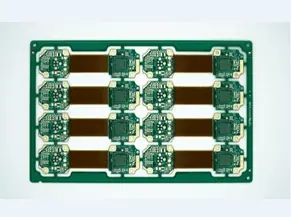
4 layer flex PCB are used in a variety of industrial applications. Our flex PCBs are first choice for industries such as power, automobile, medical devices, GPS, and industrial control equipment, to name a few.

Four Layer Flex PCB Stack up
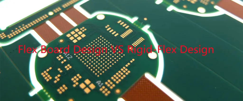
4 layer flexible PCB

Introduction

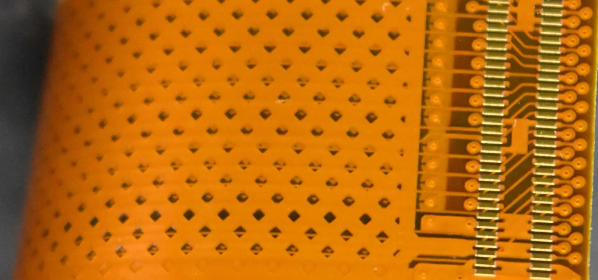
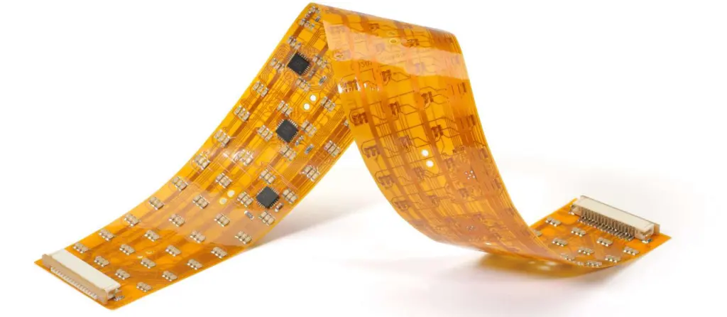
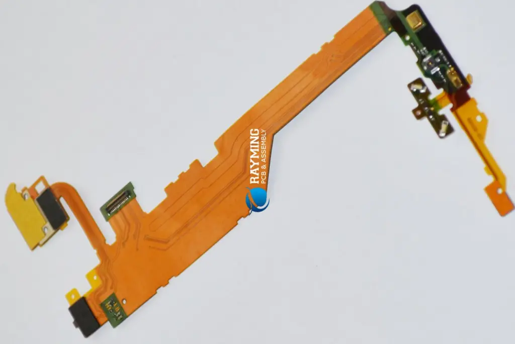
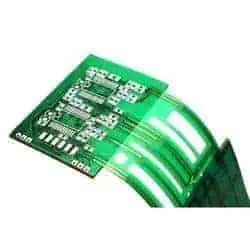
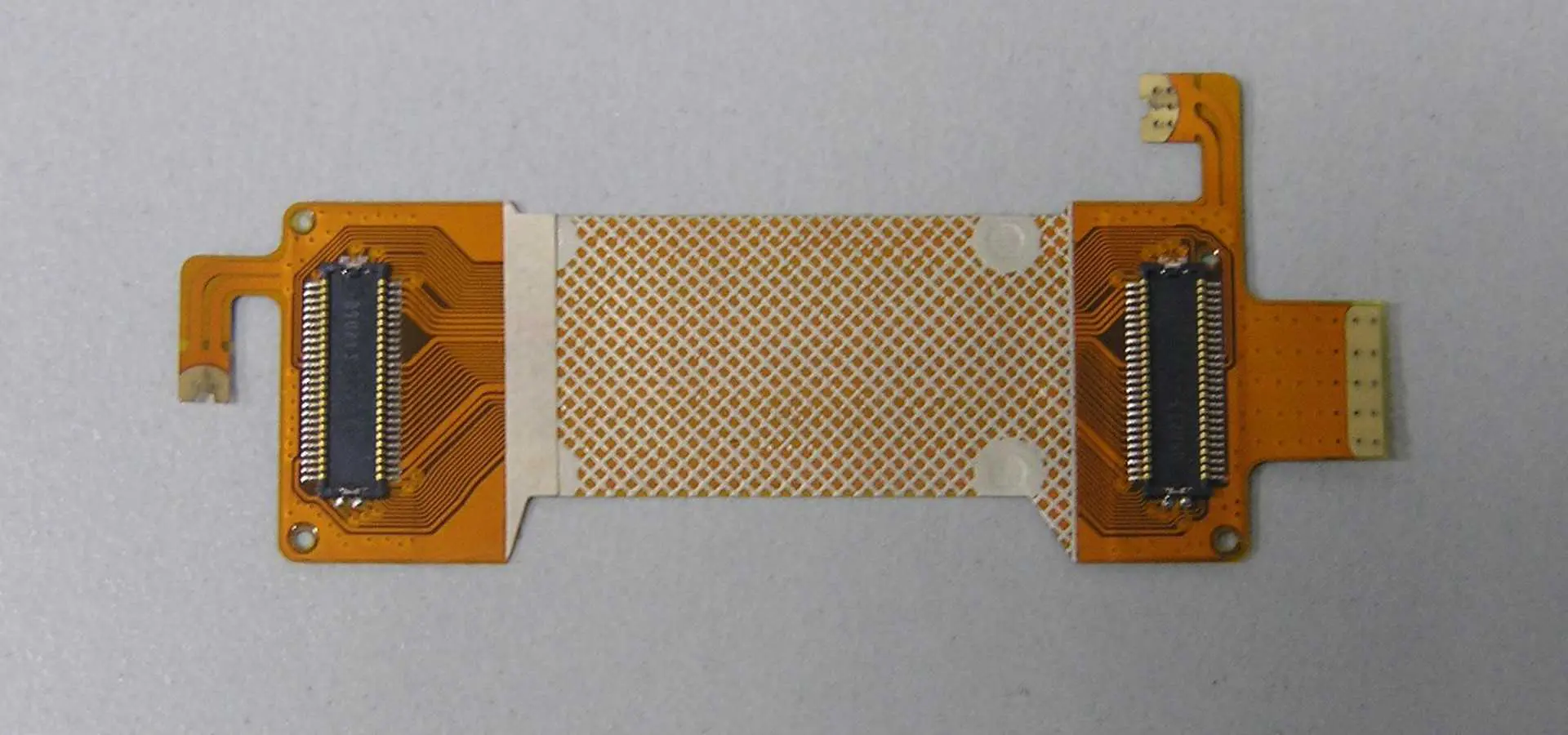
Flexible printed circuits (FPCs) provide invaluable dynamic flexing and shape conforming capabilities in electronics. 4 layer flex PCBs with conductors on 4 layers enable increased routing density and integration versus 2 layer flex, while retaining excellent flexibility.

This article examines 4 layer flex stackup configurations, critical design guidelines, the manufacturing challenges involved, advanced capabilities needed for quality 4 layer FPCs, and techniques for optimizing performance.

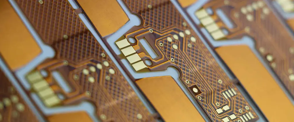
What is a 4 Layer Flex PCB?

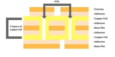
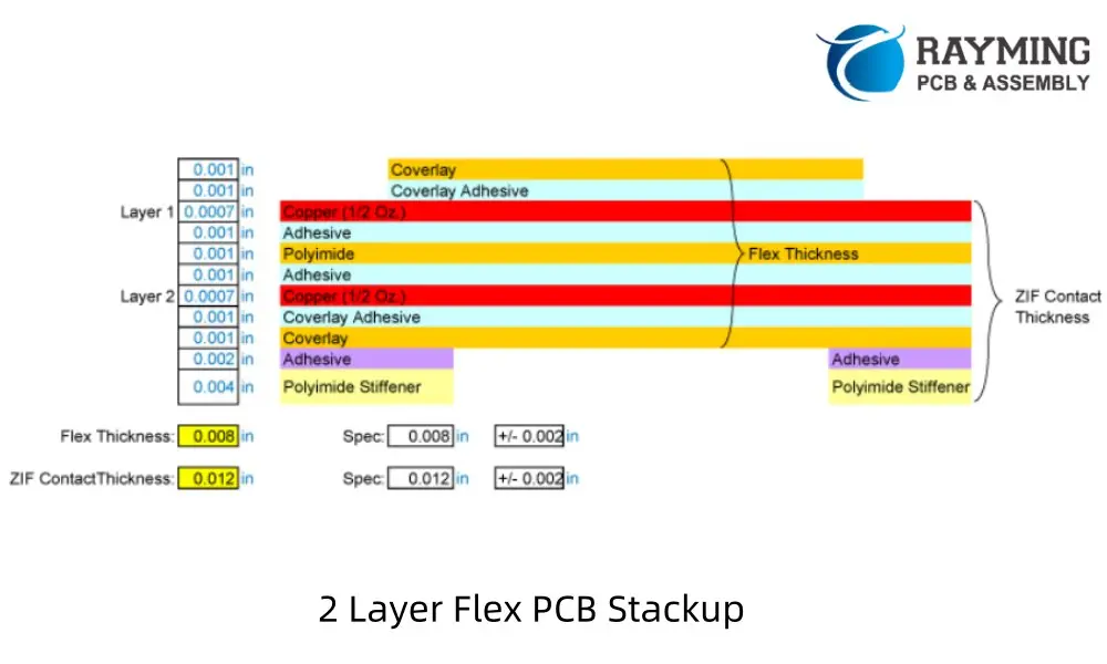
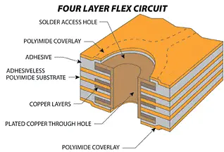
A 4 layer flex PCB consists of:

  • Flexible base dielectric material such as polyimide forming the core.
  • Copper foil conductors patterned on the top, bottom and two inner layers of the core.
  • Cover layers laminated above and below for insulation, abrasion resistance and stiffness.
  • Plated through holes (PTH) and buried vias for vertical interconnections.
  • Edge contacts or stiffeners to provide external connections.

This construction provides the highest routing density on a flex PCB with fine conductors and clearances.

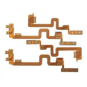
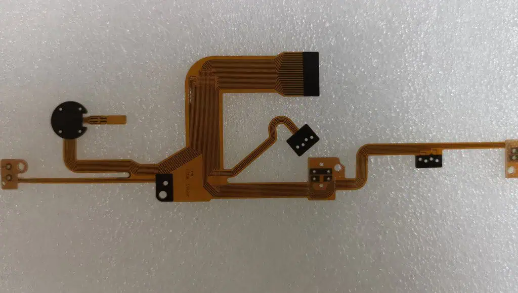
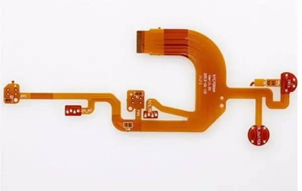
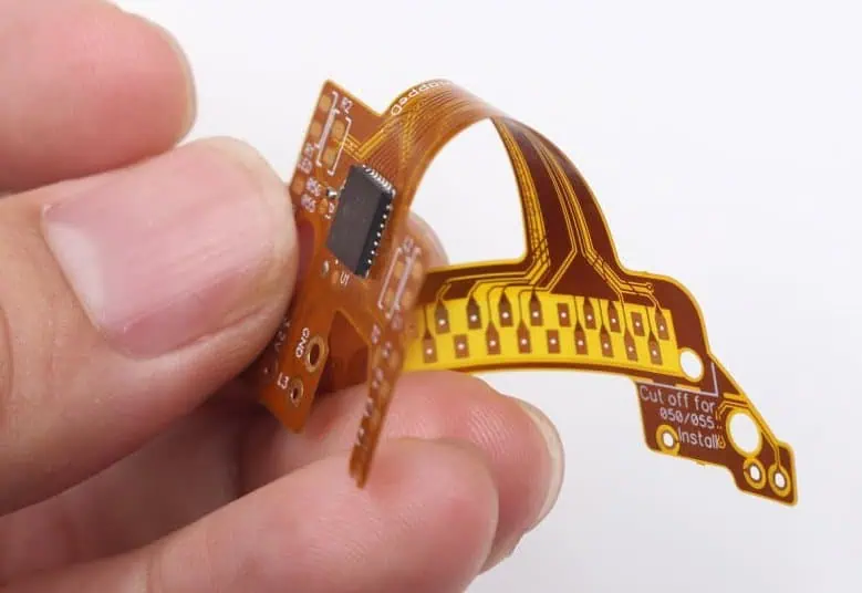
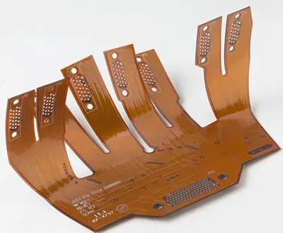
Applications of 4 Layer Flex Circuits

Some common applications leveraging 4 layer flex PCB technology include:

  • Wearable devices – Smart watches, fitness trackers, AR/VR headsets.
  • Flexible displays – Edge or foldable displays, large LED video walls.
  • Automotive – In-car displays, lane departure systems, LiDAR.
  • Aerospace/Military – Helmet systems, communications, guidance systems.
  • Medical – Ultrasound transducers, implants, endoscopes.
  • Industrial – Flexible HMIs, robotic interconnects, motion control.
  • Consumer Electronics – Foldable phones, cameras, portable electronics.

The ultra-dense interconnect capabilities of 4 layer FPCs supports the complex, compact and lightweight requirements of these applications.

Benefits of 4 Layer Flexible PCBs

Some key advantages of 4 layer flex PCBs are:

  • Maximum routing density – Complex, compact layouts with traces on 4 layers.
  • Embedded discrete passives – Buried resistor, capacitor and inductor integration.
  • Controlled impedances – Tight impedance control for matched high speed signals.
  • Integrated shielding – Entire layers can provide EMI/RFI isolation.
  • Higher component density – More components in a given area with multilayer escape routing.
  • Multilayer stacking – Can integrate other flex or rigid-flex layers.
  • Greater functionality – High density interconnects enable more capabilities and features.
  • Miniaturization – Ideal for complex circuits in small, lightweight products.
  • Lower assembly costs – Eliminates separate flexible cabling and connectors.
  • High frequency performance – Controlled impedances benefit RF applications.

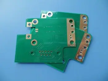
4 Layer Flex PCB Stackup Configurations

Common 4 layer flex stackup arrangements include:

Symmetrical Arrangement

Coverlayer Signal Layer 1
Ground Plane Signal Layer 2 Flexible Core Dielectric Signal Layer 3 Ground Plane Signal Layer 4 Coverlayer

This offers good EMI control with ground plane shielding and similar layer structures on both sides of the core.

Asymmetrical Arrangement

Coverlayer Signal Layer 1 Ground Plane 1 Power Layer
Flexible Core Dielectric Signal Layer 2 Ground Plane 2 Signal Layer 3 Coverlayer

Here power and ground planes are distributed on each side of the core dielectric to provide isolation between signals.

High Speed Arrangement

Coverlayer Signal Layer 1 Ground Plane 1 Signal Layer 2 Flexible Core Dielectric Signal Layer 3 Signal Layer 4 Ground Plane 2 Coverlayer

Fast signals demanding impedance control are assigned to the outer layers in this configuration. Power and ground planes provide constant reference planes.

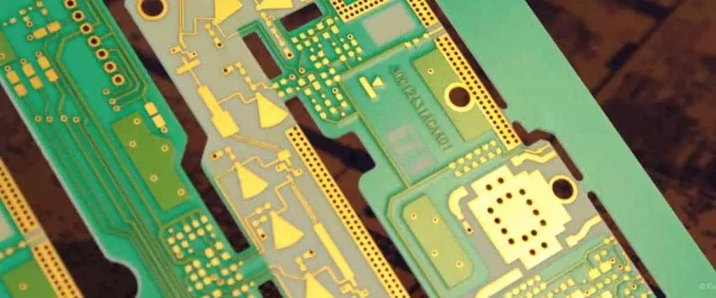
Challenges in 4 Layer Flex PCB Fabrication

While delivering substantial benefits, producing 4 layer flex PCBs poses difficulties:

  • Achieving fine lines and spaces on multiple flexible layers.
  • Holding tight layer-to-layer registration through all photolithography stages.
  • Producing high density of buried and blind microvias with thin dielectric.
  • Preventing lifted lands or cracked barrel plating on PTHs during flexing.
  • Maintaining reliable coverlayer and stiffener adhesion through dynamic flexing.
  • Controlling characteristic impedances across multiple flex layers.
  • Managing thermomechanical stresses and fatigue prone areas.
  • Qualification testing of impedance shifts under long term flex cycling.
  • Ensuring flex fold and bend cycle life reaches millions of cycles.

Advanced Manufacturing Capabilities Required

Flexible Printed Circuit Board Manufacturers

To reliably fabricate 4 layer flex circuits, PCB manufacturers need substantial expertise:

  • Fine line etching – Trace/space widths down to 25μm on multilayer flex materials.
  • Registration accuracy – Alignment of +/- 50μm between flexible layers.
  • Microvia construction – Laser drilled and plated blind/buried vias with 1:1 capture pads.
  • ANNULAR ring control – Producing 1 mil rings reliably on buried microvias.
  • Multilayer bonding – Interlayer peel strength over 2.5N/mm without delamination.
  • Surface finish – Immersion silver with thickness uniformity of <10% across flex contours.
  • Impedance tolerance – Tight impedance control within 5% of target value.
  • Flexible solder mask – Liquid photoimageable (LPI) solder mask optimized for flexing.
  • Reliability testing – Extreme temperature cycling, twisting, bending, vibration and drop testing.
  • Process Control – Real-time statistical process monitoring and control.
  • Flex fold engineering – Precisely defined and characterized bend radiuses backed by extensive test data.

4 Layer Flex Design Recommendations

Some key guidelines when designing 4 layer flex PCBs:

  • Plan stackup arrangement to isolate critical signals using ground planes.
  • Use impedance matched traces with adequate shielding for high speed signals.
  • Model impedances and performance under dynamic bending conditions.
  • Widen trace/space dimensions in flexing areas relative to rigid sections.
  • Incorporate strain relief structures at interfaces between rigid and flex sections.
  • Utilize thermal reliefs for solder joints to reduce stresses.
  • Add stiffeners or covers for rigidity at connection points.
  • Maximize distance of components from high flex zones.
  • Define and specify multiple controlled bend radii rather than arbitrary flexing.
  • Review layouts for susceptibility to acid traps during fabrication.
  • Specify microvia capture pads with 1:1 aspect ratio for reliability.
  • Consider needs for shielding, insulation and abrasion resistance in stackup design.

Conclusion

4 layer flex PCB technology enables innovative products with maximum routing density combined with dynamic flexing capabilities. To harness these benefits requires proper stackup configurations, controlled processes, and sound flex design techniques. Partnering with an expert flex PCB manufacturer having robust 4 layer technology maturity allows designers to fully leverage the advantages of 4 layer flex to develop cutting-edge solutions for flex electronics integration needs across industries.

2 layer flex pcb stackup and Manufacturing

2 layer flex pcb board
double sided flex PCB

Double-Sided Flexible PCB : Double-sided flex PCB feature two conductive layers with a layer of polyimide insulation between them. The conductive layer’s outer sides can be either exposed or have covers, like a copper pad. Layers are connected typically by plated through-holes, but other methods can be used. Like the single-sided flexible circuits, the double-sided flexible PCB can support additional elements such as pins, connectors and stiffeners.

Double Sided Flexible PCB Stack Up

Double Sided Flexible PCB

Introduction

Flexible printed circuits (FPCs) enable unique capabilities like dynamic flexing and conforming to surfaces which are not possible with rigid boards. 2 layer flex PCBs with conductors patterned on both sides of a dielectric offer more interconnect density versus single sided flex, while retaining excellent flexibility.

This article examines 2 layer flex stackup configurations, critical design considerations, the manufacturing challenges involved, advanced capabilities needed for quality 2 layer FPCs, and guidelines for optimizing performance.

What is a 2 Layer Flex PCB?

flexible circuit board

A 2 layer flex PCB consists of:

  • Flexible base dielectric material such as polyimide. This forms the core.
  • Copper foil conductors patterned on both sides of the base material.
  • Cover layers laminated over the etched traces for insulation, abrasion resistance and stiffness.
  • Plated through holes (PTHs) for interconnecting between conductors on each side.
  • Edge contacts or stiffeners to provide external connections.

The 2 metal layers bonded to a thin, flexible core dielectric provide a robust flex circuit construction with enhanced interconnect density versus single sided FPCs.

Applications of 2 Layer Flex Circuits

Some common applications of 2 layer flex PCB technology include:

  • Displays – Flexible OLED displays, curved touch sensors.
  • Automotive – Seat control panels, steering wheel electronics.
  • Consumer Electronics – Foldable phones, wearables, VR headsets.
  • Medical – Catheters, implants, transdermal patches.
  • Robotics – Flexible cabling for manipulator joints.
  • Defense/Military – Rugged flexible electronics, avionics systems.
  • Industrial – Flexible sensors, actuators, kontrollers.

The compactness, dynamic flexing and extended cycle life of 2 layer FPCs make them well suited for these applications.

Benefits of 2 Layer Flex PCBs

Some key advantages of 2 layer flex PCBs are:

  • Double routing density – Traces and componenets on both sides doubles layout area.
  • Integrated shielding – Ground planes can shield signals from EMI/RFI.
  • Embedded components – Passives can be embedded within flex layers.
  • Impedance control – Better impedance matching with sandwiched microstrips.
  • Higher interconnection density – More interconnects with fine traces on two sides.
  • Rigid sections – Can incorporate stiffened sections for component mounts.
  • Smaller product size – High density flex packing enables miniaturization.
  • Lower assembly cost – Fewer discrete wires and connectors to assemble.
  • Three-dimensional – Dynamic shaping and folding around structures.
  • High frequencies – Controlled impedances benefit high frequency performance.

2 Layer Flex PCB Stackup Configurations

Typical stackup structures used in 2 layer flex PCBs include:

Coverlayer Based Stackup

Coverlayer 1
Signal Layer 1 Flexible Core Dielectric Signal Layer 2 Coverlayer 2

This offers good abrasion resistance and insulation with coverlayers enveloping the conductors.

Adhesive Based Stackup

Signal Layer 1 Bonding Adhesive Flexible Core Dielectric Bonding Adhesive Signal Layer 2

Here the core dielectric is sandwiched between conductors using adhesive bonding films. Provides ultra-thin profile.

Copper Clad Stackup

Signal Layer 1 Flexible Core Conductor Signal Layer 2

In this case, the flexible copper clad dielectric itself functions as the core, removing the need for bonding. Can be cost-effective.

Shielded Stackup

Coverlayer 1 Signal Layer 1 Flexible Core Dielectric Ground Plane 2 Signal Layer 2 Coverlayer 2

The embedded ground plane provides shielding between signals and blocks EMI.

Challenges in 2 Layer Flex PCB Manufacturing

While providing many benefits, fabricating 2 layer flex PCBs poses manufacturing difficulties including:

  • Achieving and maintaining fine line resolution on both sides.
  • Tight layer-to-layer registration across two flexible sides.
  • Preventing delamination or separation between layers.
  • Producing plated through holes with adequate annular rings.
  • Controlling impedances across dynamically flexing layers.
  • Avoiding rigid sections from detaching on flexing.
  • Managing thermomechanical stresses from flexing.
  • Maintaining solder joint integrity across flex cycles.
  • Handling, processing and assembling extremely thin circuits.
  • Ensuring flexibility and performance with embedded passives.
  • Qualifying and modeling impedance shifts under various flex configurations.

Advanced Manufacturing Capabilities Needed

semi-flex-pcb

High quality 2 layer FPC production requires manufacturers to demonstrate several advanced capabilities:

  • Fine line etching – Trace/space down to 25μm on thin flex cores reliably.
  • Registration accuracy – Alignment around 50 to 75μm between flex layers.
  • Annular ring control – Producing 1 mil annular rings on small PTHs.
  • Flexible solder masks – Halogen-free liquid photoimageable (LPI) masks.
  • Reliable multilayer bonding – Interlayer peel strengths above 2 N/mm without delamination.
  • Surface finish – Uniform plating thickness of immersion Ag or Sn across dynamic contours.
  • Fine space via tenting – Protecting ultra-fine trace gaps during PTH drilling.
  • Flex fold engineering – Highly controlled folding with extensive test data.
  • Plated through holes – Smooth, void free copper plating of PTHs with 1:1 aspect ratio.
  • Process control – Real-time Statistical Process Control (SPC) for stability.

Reliability testing – Dynamic bend cycling, twist, vibration, thermal shock, drop testing.

2 Layer Flex PCB Design Considerations

Some key design aspects when working with 2 layer flex circuits include:

  • Modeling electrical performance under different bend configurations and cycles.
  • Assigning critical signals requiring impedance control or low skew to outer layers.
  • Using wider traces than rigid PCBs and allowing adequate spacing between traces.
  • Adding shielding planes or ground fills if EMI is a concern.
  • Using linear routing for traces along the bend axis and minimizing perpendicular traces.
  • Watching for impedance variations at transitions between rigid and flex sections.
  • Accounting for registration shifts between layers during dynamic flexing.
  • Providing sufficient annular ring margins around plated through holes.
  • Ensuring vias have 1:1 capture pad aspect ratios for reliability.
  • Incorporating thermal reliefs to reduce thermomechanical solder joint stresses.
  • Adding EMI shielding vias around components if needed.
  • Utilizing stiffeners, encapsulation and strain relief structures at stress points.

Conclusion

2 layer flexible PCBs enable increased routing density and the ability to integrate shielding planes while retaining excellent dynamic flexing capabilities. Harnessing these benefits requires mature flex PCB manufacturing processes and disciplined design techniques tailored for flex. When designed properly, robust 2 layer flex circuits provide electronics engineers an invaluable technology for developing innovative, compact and motion-tolerant products.

What is Single Sided Flexible PCB?

one layer flex pcb board

Single Sided Flexible PCB 

Single sided Flex PCB

single sided Flex PCB are the most basic type of flexible circuits. They consist of a flexible dielectric film laminated to a single sheet of copper. The copper layer is then chemically etched according to the specified circuit pattern design. Polyimide cover lays can be added to the circuit board for additional insulation and protection, if desired.

single side Flexible PCB Stack up

Single-Sided Flexible PCB : This design includes a single conductive copper layer that can   be bonded between two layers of insulation or built with one polyimide insulating layer and an uncovered side. The interior copper layer then goes through a chemical etching process, producing the circuit design. Single-sided flex PCB board designs support the inclusion of electronic components, connectors, pins and stiffeners.

Learn more about:

Introduction

Printed circuit boards (PCBs) provide the interconnect foundation in electronics products. While rigid boards are most common, flexible PCBs (FPCBs) offer unique advantages for applications requiring dynamic flexing, bending or shaping around structures. Single sided flex circuits with conductors only on one side are the simplest FPCB construction.

This article will examine what single sided flexible PCBs are, their typical applications and benefits, materials and construction methods used, critical manufacturing capabilities needed, and key design considerations when implementing single sided flex circuits.

What is a Single Sided Flex PCB?

flex pcb capability

A single sided flexible PCB consists of:

  • A flexible dielectric base made of polyimide or other flexible polymer substrates.
  • Conductive copper traces etched on one side of the base material.
  • No conductors or dielectric on the reverse side.

This provides a thin, lightweight and highly bendable circuit layer with traces on only one side. Connections to the conducting layer are made using:

  • Plated through holes (PTHs) drilled through the base substrate.
  • Edge contacts formed along one or more edges of the circuit.
  • Metal stiffeners or connectors soldered to pads on the flex layer.

Applications of Single Sided Flex Circuits

Some common applications of single sided flex PCB technology include:

  • Wearable devices – Fitness trackers, smart watches, health monitoring devices.
  • Displays – Flexible displays, electronic signage and indicators.
  • Medical – Catheters, implants, transdermal patches.
  • Automotive – Seat heaters, capacitive switches, sensors.
  • Consumer Electronics – E-readers, headphones, VR headsets.
  • Robotics – Flexible cabling for joints and manipulators.
  • IoT devices – Flexible sensor nodes and connectors.

The dynamic flexing and continuous motion capabilities of single sided FPCBs suit them for these applications.

Benefits of Single Sided Flexible PCBs

Some key benefits of single sided flex circuits versus rigid boards are:

Dynamic Flexing – Can withstand extensive flexing and shape change required in motion applications.

Lightweight – Weigh 60-80% less than equivalent rigid boards.

Thin profile – As thin as 25μm flex layers permit tight installations and stacking.

High density – Finer lines/spaces allow dense interconnections in small areas.

Three-dimensional – Can bend and conform to 3D surface shapes.

Embedded passivesCapacitors and resistors can be screened for compactness.

Low cost – Eliminates components, connectors and simplifies assembly.

High frequency – Controlled impedances and unattenuated signals at high frequencies.

Durability – Polyimide materials withstand millions of flex cycles.

Aesthetics – Can produce stylish, low profile products.

Single Sided Flex PCB Materials

Typical materials used to fabricate single sided flex PCBs include:

Base Dielectric – Polyimide is most common. Can also use LCP, PEN, PET, PU. Polyimide provides the highest flexibility and temperature durability.

Conductor – Electrodeposited copper foil, typically 12-35μm thickness. Rolled annealed copper offers optimal flexure performance.

Bonding Adhesive – Acrylic or epoxy based adhesive films attach stiffeners, connectors or components.

Cover layer – Optional polyimide or adhesive covers can be added for insulation or stiffness.

Stiffeners – Selective FR4 stiffeners may be added in flex areas requiring rigid mounting surfaces.

Finishes – Immersion tin or silver over nickel are typically used for solderability and durability.

Critical Manufacturing Capabilities

Single-sided Flex PCB

Producing robust, reliable single sided flex PCBs requires advanced manufacturing expertise:

  • Fine line etching – Ability to reliably produce and hold trace widths/spaces down to 50μm.
  • Registration accuracy – Tight process control to meet registration tolerances around 50-75μm .
  • Surface finish uniformity – Consistent immersion silver or tin plating thickness across flex circuits.
  • Quality laminating – Eliminating delamination or separation failures through process controls.
  • Flex fold engineering – Highly controlled folding based on extensive modeling and testing data.
  • Conductor adhesion – Adhesion strength of copper traces exceeding 1.5N/mm on polyimide.
  • Plated through holes – Smooth, void free copper plating of small through holes.
  • Panel handling – Special carriers, tooling and protocols to avoid damage to flex layers.
  • Reliability testing – Environmental testing, dynamic flex cycling, vibration and shock exposure.

Process control – Statistical control and continuous improvement for process stability.

Single Sided Flex PCB Design Considerations

Key design aspects when implementing single sided flex boards include:

  • Trace widths and spacing – Use wider traces than rigid boards as narrow traces may break on flexing. Space traces adequately apart for flexibility.
  • Trace routing – Route traces linearly in the direction of bending rather than perpendicular to the flex axis. Avoid sharp turns.
  • Bend areas – Use fewer traces in sections that undergo maximum bending. Add stiffeners if needed.
  • Bond pad openings – Allow for adequate bonding material around component pads for shear strength.
  • Annular rings – Maintain sufficient annular rings around plated through holes for adhesion.
  • Fold compensation – Account for swelling of outer side and shrinkage of inner side when folded.
  • Adhesives – Select flexible adhesives optimized for flexing rather than rigid bonds.
  • Reinforcements – Add stiffeners and backing structures selectively in high stress areas.
  • Termination – Use robust, flexible solderable edge connector contacts.
  • Impedances – Model electrical performance under various flex configurations.

Conclusion

With their unmatched dynamic flexing capabilities, light weight and thin profile, single sided flexible PCBs enable many new innovative applications not possible with rigid boards. When implementing single sided flex circuits, working with an expert manufacturer and following sound design practices allows harnessing the unique benefits of flex PCBs successfully. As electronics strive for greater motion tolerance, flexibility and structural integration, single sided flex PCB technology provides an enabling interconnect platform.

What is 0.6mm Thickness PCB?

0.6mm pcb thickness
0.6mm pcb

0.6mm PCB is middle thickness of printed circuit board,For double sided PCB is normal,Now more 4 layer and 6 layer PCB use 0.6mm thickness to fix smaller and thinner electronic device .

The laminate thickness as per your specifications and needs. Though, our team offers a standard thickness of 1.6 mm (0.063 inch). Sometimes, the circuit board core thickness and soldermask coating must be considered for trace impedance. When computing impedance, the consequences of conformal coating must be taken into account as the circuit boards are usually covered in soldermask. In general, soldermask decreases the impedance on thin traces. The soldermask has considerably less effect when the trace thickness increases.0.6mm pcb is common for our production, We did 4 layer 0.6mm PCB, 6 layer 0.6mm PCB, and 0.8mm PCB manufacturing.

Circuit board finish differs in rates, availability, serviceable life, consistency and assembly processing. As each finish has its individual advantages, product, the procedures, or setting will define the appropriate surface finish that is suitable for the application. We recommend our users and the designer to constantly coordinate with us for selection of ideal finish for the required product design. This will ensure you have better prices for the end product delivery.

Introduction

Printed circuit boards (PCBs) provide the foundation for mounting and interconnecting electronic components in products. PCB thickness is an important design parameter that affects weight, stiffness, manufacturability and cost. With the trend towards miniaturization in electronics, thinner PCBs around 0.6mm are increasingly being used in dense and compact designs.

This article will examine what 0.6mm PCB thickness means, the manufacturing capabilities needed, key applications for 0.6mm boards, their benefits versus standard 1.6mm PCBs, optimal stackup configurations, and design considerations when using 0.6mm PCB technology.

What Does 0.6mm Thickness Mean?

The thickness of a PCB refers to the total height of the finished multilayer board assembly including conductors, insulating dielectric material and plating finishes. Some standard PCB thickness classes are:

  • 1.6mm – Standard thickness
  • 1.0mm – Typical thinner PCB
  • 0.8mm – Mid-range thin PCB
  • 0.6mm – Ultra-thin PCB
  • 0.4mm – Extremely thin PCB

So a 0.6mm thickness PCB has an overall board height of 0.6mm. This is achieved by using thinner dielectric core and prepreg laminate materials during multilayer PCB fabrication. The thinner laminates enable reducing weight by over 60% compared to standard 1.6mm boards.

Why Use Thinner 0.6mm PCBs?

The key drivers for adopting thinner 0.6mm PCB technology are:

  • Reduce product weight and size for portability
  • Allow greater component density with thinner dielectrics
  • Enable tighter spacing and gap control for denser routing
  • Match thickness with thinner flex-rigid sections in a design
  • Allow additional layers within constrained height envelopes
  • Facilitate integration in thin packages like laptops and tablets
  • Lower material content for cost reduction

For space and weight constrained products, 0.6mm PCBs help achieve miniaturization, portability and integration goals while providing maximum functionality.

Typical Applications of 0.6mm PCBs

Some examples of products that typically utilize 0.6mm thin PCB technology are:

  • Smartphones and tablets
  • Wearable devices
  • IoT endpoints
  • Drones
  • Robotics
  • Laptops
  • Biomedical devices
  • Automotive sensors

The compact, lightweight nature of these applications makes 0.6mm PCBs suitable to facilitate greater densification and packaging flexibility with reduced thickness and mass.

Fabrication Challenges with 0.6mm Boards

rogers substrate

While providing advantages, reliably manufacturing 0.6mm multilayer PCBs poses some fabrication difficulties including:

  • Maintaining registration across multiple thin laminates
  • Achieving high peel strengths between thin cores
  • Preventing resin starvation during lamination
  • Controlling line width and spacing on thin substrates
  • Producing robust multilayer 0.6mm board stackups
  • Minimizing handling damage of flexible thin cores
  • Keeping thin panels stable and warp-free post-etching
  • Achieving desired impedance tolerances

These issues require stringent process control capabilities from the PCB manufacturer.

Key Manufacturing Capabilities for 0.6mm PCBs

To reliably produce 0.6mm multilayer PCBs, manufacturers need to demonstrate several critical capabilities:

  • Registration accuracy – +/- 0.075mm or better registration control.
  • Lamination – Expertise in bonding thin cores using high fillers to avoid voids.
  • Etching – Ability to hold 2 mil lines and spaces on 0.6mm cores.
  • Plating adhesion – Copper bond strength over 4.5N on 0.6mm dielectric.
  • Surface finish – Uniform electrolytic plating thickness across thin panels.
  • Handling – Special carriers and automation to avoid scratches, dents.
  • Stackup design – Modeling and engineering optimal 0.6mm layer configurations.
  • Flatness control – Warp/twist containment through prepreg intervals and balancing.
  • Impedance tolerance – Tight impedance matching within 5% of target.
  • Reliability testing – Thermal shock, temperature cycling, drop/shock testing.

Benefits of 0.6mm vs Standard 1.6mm PCBs

Here is a comparison between typical 0.6mm and standard 1.6mm PCB characteristics:

Parameter0.6mm PCB1.6mm PCB
Thickness0.6mm1.6mm
WeightLower by ~60%Higher
LayersTypically 4-8Typically 2-6
Line Width2 mil capable3 mil typical
Dielectric ConstantConsistentMore variation
Impedance ToleranceTighterLarger tolerances
FlexibilityFlexibleRigid
HandlingNeeds careful handlingEasily handled
Routing DensityHigher, finer featuresLower, larger features
Thermal IssuesLess heat spreadingBetter thermal conduction
ManufacturingTighter process control neededLarger process margins

Optimized Stackup for 0.6mm PCBs

Rogers TC600 PCB

To achieve a robust, reliable 0.6mm board stackup, considerations include:

  • Use thinner dielectrics like 0.2mm or 0.3mm prepregs to conserve total thickness.
  • Incorporate microvias to transition between layers, avoiding through hole vias.
  • Include power and ground planes adjacent to signal layers for isolation.
  • Watch out for impedance discontinuities at layer transitions.
  • Model key signals in PCB analysis tools to shape stackup.
  • Alternate plane directions to balance stresses and avoid warping.
  • Limit asymmetric compositions which produce curl/twist.
  • Allow extra thickness for surface finishes like ENIG or immersion silver.
  • Increase metal core layers if stiffness must be enhanced.
  • Add stiffeners or metal backers selectively if needed.

Design Considerations for 0.6mm PCBs

To effectively leverage 0.6mm boards, engineers should factor in:

  • Accounting for flexibility and handling issues in assembly processes.
  • Minimizing mechanical stresses on the thin boards in the product enclosure.
  • Watching for impedance discontinuities and reflections at layer transitions.
  • Isolating or shielding any sensitive high-speed signals on inner layers.
  • Including thermal relief connections for surface mount parts prone to heating.
  • Measuring temperature rises during operation to avoid hot spots.
  • Reviewing component layouts and spacings for optimal thermal performance.
  • Adding selective stiffening elements if board flexing causes issues.
  • Allowing for higher layer counts within given product height constraints.

Conclusion

With increasing demands for lightweight and thinner products, 0.6mm PCB technology enables reduced mass and size while packing in electronics functionality through greater routing density and layer counts. But achieving robust 0.6mm boards requires advanced manufacturing expertise. With an optimized stackup design and accounting for the unique thermal/mechanical considerations, 0.6mm PCBs can provide a platform for cutting-edge compact product development.

High Quality 0.4mm Thickness PCB Manufacturer

0.4mm pcb thickness board
0.4mm pcb

0.4mm PCB Thickness is a start for multilayer PCB , Almost is minimum thickness for PCB engineer to design a Multi-Layer boards

An extensive range of finished PCB thicknesses can be accomplished with the combination of different core thicknesses and sheets of prepreg. However, the variety of laminate thickness options offered to our customers are range from 0.008 inches to 0.240 inches and they include 0.2 mm (0.0079 inch), 0.4 mm (0.016 inch), 0.5 mm (0.020 inch), 0.6 mm (0.024 inch), 0.8 mm (0.032 inch), 1.0 mm (0.04 inch), 1.2 mm (0.047 inch), 1.5 mm (0.062 inch), 1.6 mm (0.063 inch), 2.0 mm (0.079 inch), 2.3 mm (0.091 inch), etc.

The board thickness is the thickness given in mm of the base material measured including copper foil on top and bottom. So the board thickness does not represent the final thickness of the PCB as for that we need to add plating, solder mask, etc,if you need 0.4mm final thickness , then we will use 0.3mm raw material to manufacture your PCB board .

Rayming PCB Thickness range :

0.2mm PCB         0.4mm PCB         0.6mm  PCB            0.8mm  PCB

1.0mm PCB         1.2mm PCB           1.5mm PCB             1.6 mm PCB

2.0mm PCB         2.4mm PCB          3.0mm  PCB           3.2mm  PCB

3.6mm PCB       4.8mm  PCB           5.6mm PCB

Introduction

As electronics devices continue getting smaller and more compact, demand is rising for thinner PCBs using 0.4mm laminates. However, producing reliable, high density multilayer boards at 0.4mm thickness poses significant fabrication challenges. Partnering with an experienced PCB manufacturer having expertise in 0.4mm PCB manufacturing is key to ensuring optimal quality and performance.

This article provides electronics engineers an overview of 0.4mm PCB capabilities, manufacturing process requirements, quality benchmarks, and the benefits of selecting a premier 0.4mm PCB supplier.

What is a 0.4mm Thickness PCB?

QR CODE PCB
QR CODE PCB

Standard PCB dielectric thicknesses range from 0.8mm to 1.6mm generally. With rising miniaturization needs, high density interconnect (HDI) PCBs emerged using thinner 0.3mm-0.4mm dielectrics in the last decades enabling greater compactness. Some common thin core thicknesses are:

  • 1.6mm – Standard thickness
  • 1.0mm – Common thinner material
  • 0.8mm – Typical thin PCB thickness
  • 0.4mm – Ultra-thin laminate

So a 0.4mm thickness PCB uses 0.4mm thin dielectric core and prepreg materials to construct a multilayer board. This thinner structure provides reduced weight and maximum integration density in space-constrained electronic devices and packages.

Benefits of 0.4mm Thickness PCBs

Key advantages of 0.4mm PCBs versus standard 0.8mm-1.0mm boards include:

  • Thinner profile – Allows tighter vertical stacking and electronics packaging.
  • Lighter weight – Significant weight reduction for portable devices.
  • High density – Thinner dielectrics permit greater routing density.
  • Small vias – Thinner boards can use smaller microvias.
  • Low z-axis CTE – Mitigates via barrel crack issues.
  • Fine lines – Enables finer line width/space geometries.
  • High layer count – Permits more layers within a given thickness.
  • Flexibility – Easier to produce semi-flex constructions.
  • Buried passives – Allows integration of thin film capacitors/resistors.

0.4mm PCBs enable maximum density and integration where thickness is constrained.

Challenges in 0.4mm PCB Fabrication

Fabricating 0.4mm multilayer PCBs poses substantial production difficulties including:

  • Filler starvation – Ensuring adequate resin fill of thin cores during lamination.
  • Layer registration – Tolerance control across multiple thin laminates.
  • Plating adhesion – Copper to dielectric bond strength on low filler cores.
  • Hole wall quality – Resin smear and fill control of drilled holes.
  • Surface finish – Uniform plating thickness on flexed thin panels.
  • Fine line etching – Achieving 2 mil line width and space on 0.4mm cores.
  • Via reliability – Avoiding cracks due to drilling and z-axis CTE stresses.
  • Lamination bonding – Achieving high bond strength between thin layers.
  • Handling – Preventing damage like dents, scratches and pits on thin cores.
  • Stiffness – Maintaining adequate panel stability when handling thin boards.

These factors require advanced process capabilities and controls to reliably produce 0.4mm PCBs.

Key 0.4mm PCB Manufacturing Capabilities

To reliably fabricate 0.4mm multilayer PCBs, manufacturers must demonstrate several critical capabilities:

  • Registration accuracy – Within 0.075mm between layers.
  • Plating adhesion – Copper pad peel strength over 6N on 0.4mm cores.
  • Lamination – Precise pressure control and resin fill optimization.
  • Hole wall quality – Minimal resin smear inside drilled holes.
  • Surface finish – Highly uniform electrolytic plating across thin flexing panels.
  • Fine line etching – 0.15mm lines and spaces.
  • Via reliability – Thermal shock and drop/shock testing of microvias.
  • Interlayer bonding – Lamination peel strengths above 5N/mm.
  • Handling processes – Automation and special carriers to prevent damage.
  • Stiffness – Ability to hold panel flatness tolerances.
  • Reliability testing – Extensive HAST, thermal cycling and humidity/bias testing.

Meeting these benchmarks validates a company’s capabilities in high quality 0.4mm PCB manufacturing.

Benefits of Partnering with a Premier Manufacturer

shengyi-pcb

Selecting a well-established PCB company with proven expertise in 0.4mm boards provides key advantages:

  • Mitigate Technology Risk – Avoid initial issues during 0.4mm adoption through robust qualified processes.
  • Accelerate Time-to-Market – Get cutting-edge products to market faster through rapid prototyping and scaling.
  • Increase Performance Margins – Achieve maximum routing density and electrical performance.
  • Ensure Long-Term Reliability – Mature process and quality systems deliver reliable 0.4mm boards.
  • Control Costs – Leverage accumulated 0.4mm manufacturing learnings and economies of scale.
  • Simplify Logistics – Single expert source for prototypes through volume production.
  • Strategic Alignment – Collaborate on design innovations and technology roadmap.

For companies looking to utilize 0.4mm PCBs, the right manufacturing partner provides immense strategic value in capabilities, time-to-market, performance and costs.

Conclusion

As electronics devices continue getting smaller and thinner, reliably producing 0.4mm multilayer boards becomes critical but also highly challenging. Partnering with an elite PCB company that has matured 0.4mm technology provides a low risk accelerated path to adopting this essential thinner PCB technology successfully.

High Quality 0.2mm Thin PCB Manufacturer

0.6mm pcb thickness

0.2 mm PCB thickness is not usual for printed circuit board , is very thin , easy to break , special when  PCB manufacturing process, should be taken care .

0.2mm pcb

Minimum thickness PCB is a term used to describe that the thickness of a printed circuit board is much thinner than normal PCB. The standard thickness of a circuit board is currently 1.5mm. The minimum thickness is 0.2 mm for the majority of circuit boards. Due to the market demand for continually thinner devices, there is a demand for minimum thickness PCB boards such as 0.2 mm, 0.4 mm, 0.6 mm ,0.8board, etc. These circuit boards can be used in sensor cards, SIM cards, and so on.

0.2 mm PCB is normal for flexible PCB, The production process is different, so flex PCB 0.2 mm or 0.1mm is easy to produce , Japan  lamilate company also start to supply 0.1mm rigid PCB raw material , that most use in camera or some special sensor components .

Choosing a very thin PCB thickness may limit the choice of surface finishes available. Each surface finish has a different manufacturing process based on the material properties and production method. Our standard immersion gold surface finish does support 0.2mm minimum thickness PCB, while Lead Free HASL can only be applied for a minimum thickness of 0.6mm. Immersion Tin and Silver have a minimum thickness of 0.4mm.

Rayming PCB production Thickness range :

0.2mm PCB         0.4mm PCB         0.6mm  PCB            0.8mm  PCB

1.0mm PCB         1.2mm PCB           1.5mm PCB             1.6 mm PCB

2.0mm PCB         2.4mm PCB          3.0mm  PCB           3.2mm  PCB

3.6mm PCB       4.8mm  PCB           5.6mm PCB

Introduction

As electronics devices continue getting smaller and more portable, demand is rising for ultra-thin PCBs using 0.2mm laminates. However, reliably producing multilayer boards with 0.2mm thin dielectrics poses immense fabrication challenges. Partnering with an experienced PCB manufacturer that has mastered quality production of 0.2mm thin boards is key to ensuring flawless performance.

This article provides electronics design engineers an overview of 0.2mm thin PCB capabilities, manufacturing process requirements, quality benchmarks, and the benefits of selecting a premier thin PCB supplier.

What is a 0.2mm Thin PCB?

Standard PCB dielectric thicknesses range from 0.4mm to 2.0mm. High density interconnect (HDI) PCBs drove dielectric thicknesses down to 0.3mm-0.2mm over the last decade enabling miniaturization. Some common thin laminate thicknesses are:

  • 0.8mm – Standard thickness
  • 0.4mm – Common thinner material
  • 0.3mm – Typical HDI dielectric
  • 0.2mm – Ultra-thin laminate

So a 0.2mm thin PCB uses dielectric core and prepreg materials with 0.2mm thickness. This provides the ultimate in compact, thin profile PCB constructions necessary for small, lightweight devices and tight space electronics packaging.

Benefits of 0.2mm Thin PCBs

0.2mm thin pcb board

Key advantages of 0.2mm thin PCBs versus standard 0.5mm-1.0mm boards include:

  • Thinnest profile – Enables slimmest possible electronics constructions.
  • Lighter weight – Minimal material mass for lightweight mobile devices.
  • High density – Thinner dielectrics allow greater routing density.
  • Small via diameters – Thinner boards permit smaller microvias.
  • Buried passives – Allows integration of thin film capacitors/resistors.
  • Low z-axis CTE – Reduces likelihood of via barrel cracks.
  • Fine lines – Thinner cores enable finer lithographic trace geometries.
  • High layer count – More layers can be accommodated in a given thickness.
  • Embedded actives – Allows embedding tiny active components.
  • Flexibility – Easier to produce slightly flexible constructions.

0.2mm PCBs provide the ultimate in dense, thin, lightweight circuit integration.

Challenges in 0.2mm PCB Fabrication

Fabricating 0.2mm PCBs poses substantial production difficulties including:

  • Filler starvation – Insufficient resin fill of thin cores during lamination.
  • Layer registration – Tolerance control across many thin laminates.
  • Plating adhesion – Copper bond strength on low filler content thin cores.
  • Surface finish – Uniform plating thickness on flexed thin panels.
  • Hole wall quality – Resin smear and adequate resin fill of drilled holes.
  • Fine line etching – Defining 1 mil lines and spaces on 0.2mm cores.
  • Via reliability – Avoiding cracks from z-axis CTE and drilling stresses.
  • Lamination bonding – Bonding strength between thin dielectric layers.
  • Handling – Preventing damage like scratches and dents on thin cores.
  • Stiffness – Maintaining panel stability without excessive flexing.

These factors require stringent process controls and inspection capabilities to produce reliable 0.2mm PCBs.

Key 0.2mm PCB Manufacturing Capabilities

To reliably fabricate 0.2mm multilayer PCBs, manufacturers must demonstrate several advanced capabilities:

  • Registration accuracy – Within 0.05mm between layers.
  • Plating adhesion – Copper pad peel strength over 4.5N on 0.2mm cores.
  • Lamination – Precision pressure control and resin fill optimization.
  • Fine line etching – 0.1 mm lines and spaces.
  • Hole wall quality – Minimal resin smear inside drilled holes.
  • Surface finish – Uniform electrolytic plating across thin panels.
  • Via reliability – Thermal shock and drop/shock testing of microvias.
  • Interlayer bonding – Lamination peel strengths above 3.5N/mm.
  • Handling processes – Automation and special carriers to avoid damage.
  • Stiffness and flatness – TECA & LEICA flatness measurement.
  • Reliability testing – Extensive temperature cycling, HAST, bias/humidity testing.

Meeting these benchmarks validates a company’s capabilities in high quality 0.2mm PCB manufacturing.

Benefits of Partnering with a Premier Manufacturer

Selecting an established PCB company with proven expertise in 0.2mm boards provides key advantages:

  • Mitigate Technology Risk – Avoid initial issues during 0.2mm adoption by leveraging robust qualified processes.
  • Accelerate Time-to-Market – Get cutting-edge products to market faster through on-demand prototypes and rapid scaling.
  • Increase Performance Margins – Achieve maximum possible routing density and electrical performance.
  • Ensure Reliability – Mature process and quality systems deliver ultra-reliable 0.2mm boards.
  • Control Costs – Leverage accumulated 0.2mm manufacturing learning and economies of scale.
  • Simplify Logistics – Single expert source for prototypes through high volume production.
  • Strategic Alignment – Roadmap technology innovations jointly.

For companies looking to harness the advantages of 0.2mm PCBs, the right manufacturing partner provides immense strategic value in capabilities, time-to-market, performance and costs.

Conclusion

While enabling unprecedented miniaturization, reliably producing 0.2mm thin multilayer PCBs poses immense process challenges. Partnering with an elite PCB company that has proven expertise in this highly specialized niche is key to mitigating risks and ensuring success when implementing leading-edge 0.2mm thin PCB technology.

Flex PCB Stiffeners: A Comprehensive Guide to Design and Application

pcb board stiffeners

Are you working with flexible printed circuit boards (PCBs)? If so, you’ve likely encountered the need for flex PCB stiffeners. These essential components play a crucial role in enhancing the functionality and durability of flex PCBs. In this comprehensive guide, we’ll explore everything you need to know about flex PCB stiffeners, from their uses and materials to design tips and advantages.

What are the Uses of Flex PCB Stiffeners?

Flex PCB stiffeners serve multiple purposes in circuit design:

  1. Component Support: They provide a stable platform for mounting components.
  2. Connector Reinforcement: Stiffeners strengthen areas where connectors attach to the flex PCB.
  3. Flex-to-Rigid Transition: They create smooth transition zones between flexible and rigid sections.
  4. Selective Flexibility: Designers can control which areas remain flexible and which become rigid.
  5. Protection: Stiffeners safeguard delicate components from damage due to bending or external forces.

Why Do Flex PCBs Need Stiffeners?

YouTube video

Flex PCBs require stiffeners for several reasons:

  1. Mechanical Stability: Stiffeners provide rigidity in critical areas.
  2. Improved Solderability: They offer a stable surface for soldering components.
  3. Stress Relief: Stiffeners help distribute mechanical stress evenly across the PCB.
  4. Enhanced Durability: They protect vulnerable areas from damage due to repeated bending or vibration.
  5. Ease of Assembly: Rigid areas make handling and assembly easier.
  6. Dimensional Stability: Stiffeners maintain the dimensional stability of critical areas.

Learn more about:

Flex PCB Stiffener Materials

Choosing the right stiffener material is crucial. Here are the most common options:

1. PI Stiffener

Polyimide (PI) stiffeners offer:

  • High temperature resistance
  • Chemical resistance
  • Dimensional stability
  • Flexibility
  • Lightweight properties

2. FR4 Stiffener

FR4 stiffeners provide:

  • Cost-effectiveness
  • Good electrical properties
  • Thermal stability
  • Ease of machining
  • Compatibility with PCB processes

3. Stainless Steel Stiffener

Stainless steel stiffeners feature:

4. Multiple PCB Stiffener

Some designs use a combination of materials for optimal performance:

  • Hybrid designs combining different materials
  • Tailored properties for specific areas
  • Cost optimization
  • Enhanced functionality

Common Thickness of Flex PCB Stiffeners

Flex PCB stiffener thickness varies depending on the application and material:

  • PI Stiffeners: 0.05mm to 0.5mm
  • FR4 Stiffeners: 0.1mm to 1.6mm
  • Stainless Steel Stiffeners: 0.1mm to 0.3mm
Stiffener MaterialUsual ThicknessUnusual Thickness
Polyimide (PI)0.05mm (2mil)0.175mm (7mil)
0.075mm (3mil)0.2mm (8mil)
0.1mm (4mil)0.25mm (10mil)
0.125mm (5mil)0.225mm (9mil)
0.15mm (6mil)0.25mm (10mil)
0.275mm (11mil)
FR-40.2mm (8mil)0.9mm (35mil)
0.3mm (12mil)1.1mm (43mil)
0.4mm (16mil)1.3mm (51mil)
0.5mm (20mil)1.4mm (55mil)
0.6mm (24mil)1.6mm (63mil)
0.7mm (28mil)
0.8mm (32mil)
1.0mm (39mil)
1.2mm (47mil)
1.5mm (59mil)
Aluminum0.2mm (8mil)0.15mm (6mil)
0.25mm (10mil)0.45mm (18mil)
0.3mm (12mil)
0.35mm (14mil)
0.4mm (16mil)
0.5mm (20mil)
1.5mm (59mil)
Stainless Steel0.15mm (6mil)
0.2mm (8mil)

Factors influencing thickness selection include required rigidity, space constraints, weight considerations, thermal management, and cost.

How to Connect Stiffeners to a Flex PCB?

There are several methods for attaching stiffeners to flex PCBs:

  1. Adhesive Bonding: Uses specialized adhesives for uniform stress distribution.
  2. Thermal Bonding: Applies heat and pressure for a strong, permanent bond.
  3. Mechanical Fastening: Utilizes screws or rivets for easy assembly and disassembly.
  4. Integrated Stiffeners: Incorporates stiffener materials directly into the PCB stackup.

Flex PCB Stiffener Design Tips

Follow these tips for optimal flex PCB stiffener design:

  1. Strategic Placement: Identify areas requiring rigidity and consider bending requirements.
  2. Material Selection: Choose based on application needs and manufacturing processes.
  3. Thickness Optimization: Balance rigidity requirements with overall thickness constraints.
  4. Thermal Management: Use stiffeners to aid in heat dissipation where necessary.
  5. Electrical Considerations: Evaluate the impact on signal integrity and impedance control.
  6. Manufacturing and Assembly: Design for ease of manufacturability and assembly.
  7. Testing and Reliability: Include stiffened areas in bend testing and reliability assessments.
  8. Design for Flexibility: Use flexible adhesives in transition areas and implement gradual transitions.
  9. Regulatory Compliance: Ensure materials comply with relevant industry standards.
  10. Prototype and Iterate: Create prototypes to validate design and performance.

Advantages of Using Flex PCB Stiffeners

Incorporating stiffeners in flex PCB designs offers numerous benefits:

  1. Enhanced Reliability: Reduces stress on components and solder joints.
  2. Improved Manufacturability: Facilitates easier handling during assembly.
  3. Design Flexibility: Allows for the integration of rigid and flexible sections.
  4. Cost-Effective Solution: Can eliminate the need for separate rigid and flexible PCBs.
  5. Improved Signal Integrity: Provides stable platforms for high-frequency components.
  6. Thermal Management: Can incorporate materials with good thermal conductivity.
  7. Mechanical Protection: Shields sensitive areas from external forces and impacts.
  8. Simplified Repair and Maintenance: Allows for easier replacement of wear-prone components.
  9. Customization Options: Stiffeners can be tailored to specific product requirements.
  10. Compatibility with Advanced Technologies: Supports integration of cutting-edge components.

Conclusion

Flex PCB stiffeners are essential components in modern flexible circuit design. They offer the perfect balance between flexibility and rigidity, enabling innovative electronic products across various industries. By understanding the materials, design considerations, and advantages of flex PCB stiffeners, engineers can create more robust, efficient, and advanced electronic devices.

Are you ready to enhance your flex PCB designs with stiffeners? Apply the knowledge from this guide to your next project and experience the benefits firsthand. Remember, the key to successful flex PCB stiffener implementation lies in careful planning, material selection, and design optimization.

What is Countersink Holes in PCB ?

countersink hole on pcb

2 Type  PCB Countersink Holes design , V Countersink  Holes and T Countersink  Hours . 

PCB circuit board Countersink hole

How to drill PCB Countersink Holes

Countersink-Holes board
counterbore hole

A countersink is a conical hole cut into a manufactured object, or the cutter used to cut such a hole. A common usage is to allow the head of a countersink bolt or screw, when placed in the hole, to sit flush with or below the surface of the surrounding material.

When you plan to design countersink in your board, below information is required:

Which side of countersink hole be drilled? Like Bottom Layer?
Is the countersink hole plated or non-plated?
What is countersink hole diameter(d2)?
What is through hole diameter(d1)?
What is the depth of countersink hole need to sink(t1)?
What is angle of countersink hole(like 90 degree or other)?

Fr4 PCB Countersink Holes                                       Aluminum PCB Countersink Holes

Fr4 PCB Countersink holes
Aluminum PCB Countersink hole

Introduction

A printed circuit board (PCB) is the foundation of an electronic device, providing the mechanical structure and electrical connections between components. As PCBs have become more complex, certain design techniques have been adopted to improve manufacturability and performance. One of these important features is the countersunk hole.

Countersunk holes serve several crucial functions in PCB design and fabrication. In this article, we will explore what countersunk holes are, why they are used, the different types, how to design and specify them correctly, and some best practices when using countersunk holes in a PCB design.

What is a Countersunk Hole?

A countersunk hole is a type of through-hole in a PCB that has a flared opening on one or both sides of the board. The hole is tapered, with the diameter increasing moving away from the center of the board. This flared opening provides clearance for a fastener head like a screw or bolt when secured to the PCB.

The key elements that characterize a countersunk hole are:

  • Chamfer Angle – The angle between the tapered sidewall and the planar PCB surface. Common angles are 80-100°.
  • Counterbore Depth – The depth of the chamfer or taper below the top surface of the PCB.
  • Hole Diameter – The width of the hole at the center where it passes through the board. Often the same as the fastener shaft diameter.
  • Surface Diameter – The width of the flared opening on the top (and sometimes bottom) of the PCB. This clearance allows the fastener head to sit flush with the PCB surface.

The countersink creates a smooth, flattened opening for the fastener head to sit in, allowing it to mount flush to the board surface. This is advantageous both for assembly of the components onto the board and achieving a low profile assembled product.

Why Use Countersunk Holes in PCBs?

There are several reasons why countersunk holes are extremely common in PCB designs:

Consistent Fastener Head Clearance

The tapered opening ensures consistent clearance between the fastener head and pad/trace on the board surface. Without the countersink, any small variations in board thickness, component position, or fastener length would change the clearance above the board surface. This could lead to insufficient clearance.

Flush Fastener Heads

The counterbore depth positions the fastener head flush with the PCB surface (when using flathead screws). This allows tight spacing to other components, heatsinks, and enclosure parts.

Smooth Surface Finish

No fastener heads protruding above the PCB surface gives a smooth, continuous surface ideal for EMI shielding, gaskets, and enclosures.

No Component Interference

If using pan head or other screw heads, the counterbore depth gives adequate clearance between the component and fastener head. This allows locating components near mounting holes.

Consistent Board Support

The edges of the counterbore provide consistent edge support to the PCB surface around the fastener, important for load bearing and vibrational stability.

Improved Manufacturability

A countersunk hole can ease assembly by guiding screws into the tapered opening. The clearance also allows some positioning tolerance.

Using countersunk holes whenever possible provides the most reliable PCB fastening while achieving a low-profile and compact design. The tapered opening ensures a consistent, solid fit for the fastener head.

Types of Countersunk Holes

There are two main types of countersunk holes used in PCBs, characterized according to which side the chamfer appears on.

Front Side Countersink

A front side countersink (sometimes called “countersunk”) has the tapered opening on the top layer or component side of the PCB. This allows fastener heads, such as flat head screws, to sit flush with the top surface where components are mounted.

Front side countersinks are the most common, used with any fastener that mounts components or hardware to the top surface of the board. The counterbore depth positions the fastener flush with the outer board layer.

Back Side Countersink

A back side countersink (sometimes called “counterbored”) has the tapered hole opening on the bottom side of the PCB. The straight hole walls pass through the board thickness with the chamfer on the underside.

Back side countersinks allow fastener heads to sit flush with the bottom surface. This is useful when the underside needs an unobstructed fastener profile, such as securing a PCB to a flat surface. Heat sink plates also benefit from a flat underside.

PCB Countersink Design Considerations

There are several important factors to consider when designing countersunk holes in a PCB. These parameters impact the hole’s manufacturability, component clearances, and fastener fit.

Counterbore Depth

The counterbore depth should match the thickness of the fastener head plus 10-20% clearance. This positions the fastener head flush within the chamfer opening. For example, a 4mm screw head would need ~4.5mm counterbore depth.

Insufficient depth can cause interference with components while excessive depth reduces the board support around the fastener.

Hole Diameter

The drill diameter should match the fastener shaft diameter, generally with 0.1-0.2mm clearance. Too large of a hole reduces friction and torque holding the fastener. Too small of a hole risks cracking the PCB when driving the screw.

Surface Diameter

The surface diameter must provide adequate clearance for the fastener head and any washers. About 0.25-0.5mm clearance beyond the head width is ideal for ease of assembly while minimizing unsupported board area.

Chamfer Angle

The angle between the hole wall and board surface is typically 90-100°. Larger angles over 100° provide more head clearance but less edge support and weaker laminate strength near the hole. Angles below 90° are possible but harder to manufacture.

Hole Pattern

Follow the fastener manufacturer’s recommended pattern for hole spacing relative to board edges. This avoids splitting the board or having it bend/bow under fastening force.

Plated vs Non-Plated

Countersunk holes are usually non-plated since only the top and bottom board surfaces require copper. Plated holes add unnecessary cost unless used as thru-hole vias. Non-plated holes can be plugged after drilling.

Copper Clearance

All copper on the chamfer surface must be cleared from the tapered hole. Any copper remnants create an uneven fastener interface. Remove copper at least 0.2mm beyond the surface diameter.

Annular Rings

Avoid locating pads or traces near a countersink opening. The drilled hole will not have complete annular rings, risking via breakout and limiting solder masked openings.

By carefully controlling these design factors, countersunk holes provide reliable, consistent clearance for fastener heads securing a PCB.

Specifying Countersunk Holes

Countersunk holes require several specifications when documenting the PCB layout. Different CAD tools use varying terminology and procedures for defining countersinks. However, the key parameters to communicate are:

  • Hole diameter
  • Counterbore depth
  • Surface diameter
  • Which side is countersunk
  • Chamfer angle (sometimes assumed as 90°)

For example, a backside countersunk hole for an M3 screw with 4mm head would be specified as:

  • Hole diameter: 3.1mm
  • Counterbore depth: 4.6mm
  • Surface diameter: 8mm
  • Side: Back
  • Angle: 90°

Providing these details in manufacturing drawings or CAD models ensures the PCB fabricator drills the holes properly for robust fastening.

Design Best Practices

Here are some best practices to consider when using countersunk holes in a PCB design:

  • Minimize the number of mixed hole types when possible for simpler fabrication.
  • Orient all screws/fasteners in one direction for easier assembly.
  • Cluster groups of countersunk holes together, avoiding single isolated holes.
  • Place holes in less critical board areas that are not dense with routing.
  • Allow adequate spacing around holes for laminate to absorb loads without cracking.
  • Specify tight diameter and depth tolerances for quality standards.
  • Remove all copper from chamfer area and provide annular ring clearance (>0.2mm)

Carefully following these guidelines will result in a countersunk hole design that maximizes the benefits of flush fastening while minimizing manufacturing risks.

Applications and Examples

Countersunk holes are used in nearly all types of PCB designs where mechanical fastening is required. Here are some examples:

Component Mounting

PCB standoffs use front side countersinks to allow tight spacing between boards in a stacked assembly.

Heat Sink/Cooling Plates

Processors often mount heat sinks using countersunk holes for smooth contact surface and thermal transfer.

Shielding Cans

EMI shielding cans fasten to boards with countersunk holes to eliminate gaps in conductive enclosure.

Case/Enclosure Mounting

Nearly all types of electronic enclosures use countersunk screw holes to achieve a tight fit and smooth exterior surface.

Keyed Interconnects

Some board-to-board connectors orient and key boards using countersunk holes and guide pins.

There are almost limitless examples of the versatility of countersunk holes for securing PCBs in final products across all industries and applications.

Conclusion

In summary, countersunk holes are a critical PCB design feature that enables secure, reliable mechanical assembly. The tapered hole profile allows fastener heads to sit flush with the board surface, ensuring proper clearance, orientation, and maximum surface contact.

By understanding the different types of countersinks, key design parameters, and manufacturability considerations, PCB designers can effectively leverage countersunk holes in their projects. Following the best practices outlined above will result in a robust mechanical interface for any electronic device.

The countersink is a simple yet powerful concept that facilitates cost-effective, streamlined production of complex PCB assemblies, making it an essential tool for any designer working on rigid boards.

Frequently Asked Questions

What are the key benefits of using countersunk holes in PCBs?

The main benefits of countersunk holes are:

  • Consistent fastener head clearance from components and board surface
  • Flush mounting of fastener heads for smooth exterior finish
  • Avoidance of component interference near mounting locations
  • Even support and load distribution around fasteners
  • Easier component assembly and alignment to board

Can plated-through holes be countersunk?

Yes, plated-through holes (PTHs) can be designed as countersunk holes. However, it does require more complex fabrication involving masked jet plating. Countersunk PTHs are generally more expensive and only used when electrically connecting between both sides is required.

What is the downside of excessive counterbore depth?

Too much counterbore depth leaves a thinner ring of board laminate material around the top of the hole. This can crack under fastening strain. Typically only 10-20% clearance beyond the fastener head thickness is recommended.

When should back side countersunk holes be used vs front side?

Back side countersinks allow flush fastener heads on the bottom board surface. This is advantageous when the underside requires smooth, unobstructed contact, such as for heat sinks. Front side countersinks are used in most applications to avoid component interference.

Can clearance holes be used instead of countersunk holes?

Clearance holes (straight through holes) can replace countersinks in some cases, but do not provide as reliable or consistent a fastening surface. Clearance holes may also require washers to prevent fastener heads contacting the board surface.

What is 6 Layer Rigid-Flex PCB?

rigid-flex pcb fabrication

Camera Rigid Flex PCB

Name: Camera just scratched

Rigid  Board : 6 Layer Rigid PCB

Flexible PCB 2  Layer

Board thickness: 0.9mm

Copper thickness oz: 1oz

Material: IT180A + AK

Type: Car HD Camera

Technical features: rigid-flex structure

Application: Car Camera

Introduction

6 Layer Rigid-Flex PCB

Rigid-flex PCBs provide the ability to integrate multiple rigid PCBs interconnected using flexible circuits in a single assembly. The combination of rigid and flexible materials in one board allows three-dimensional packaging and increased component density within electronic devices.

6 layer rigid-flex refers to a board stackup with 6 conductive copper layers. This article will provide an overview of 6 layer rigid-flex PCB technology covering:

  • Benefits and applications
  • Construction and materials
  • Fabrication process
  • Design guidelines
  • Assembly considerations
  • Cost impact

Benefits of 6 Layer Rigid-Flex PCBs

Compared to conventional rigid boards, 6 layer rigid-flex PCBs offer the following advantages:

Increased Component Density

Folding rigid sections vertically allows placing components on both sides of stacked boards for space and height reduction.

Simplified Assembly

Replacing discrete flexible cables and wire harnesses with integrated flexi-rigid board reduces assembly labor and errors.

Enhanced Flexibility

Eliminates inter-board connectors by running flexible circuits between rigid sections. Accommodates complex motion paths.

Improved Serviceability

Modules can be independently removed for repair/upgrade without affecting other sections by separating along flex bends.

Reduced Weight

Inter-board cables have heavier insulation than thin flexible layers.Removes extraneous housing needed for discrete cables.

Lower Costs

Fewer connectors, simpler assembly, higher density save on materials cost and manufacturing expenses.

Signal Integrity

Better high speed performance by minimizing discontinuities through maintained impedance in traces spanning rigid and flex sections.

Reliability

Avoids reliability risks associated with external wiring and interconnections.

Applications of 6 Layer Rigid-Flex PCBs

rigid-flex-pcb-design

The unique capabilities of rigid-flex make them ideal for the following applications which require packaging density, versatility and reliability:

  • Wearable devices
  • Medical electronics
  • Consumer gadgets
  • Robotics and UAVs
  • Automotive electronics
  • Industrial equipment
  • Military systems

6 layer rigid-flex technology provides adequate routing channels to implement complex high density circuits for such miniaturized and high performance products.

Rigid-Flex PCB Construction

6 layer rigid-flex consists of:

  • Multiple layers of copper clad rigid FR-4 material
  • Layers of adhesive-based flexible dielectric like polyimide
  • Coverlay bonding the flexible layers

The main rigid section has 6 copper layers. The flex sections integrate 2-6 layers depending on routing needs. Sections are held together by an adhesive. Plated thru holes provide interconnects between layers.

Rigid sections provide mechanical strength for component mounting and heatsinking. Flex layers enable out-of-plane motion and 3D assembly. Different rigid and flex materials can be combined for optimal electrical and thermal performance.

Fabrication Process

6 layer rigid-flex PCB fabrication involves:

Layer Bonding

Rigid and flex core layers are bonded together using adhesive sheets. FR-4 and polyimide are commonly used. Alignment is critical.

Hole Drilling

Mechanical and laser drilling create thru holes for layer interconnection in rigid sections.

Metallization

Copper layers are added using processes like direct plate, pattern plate and print-and-etch. Plated thru hole walls are also metallized.

Lithography

Photoimaging transfers the circuit layout onto multiple rigid and flex layers.

Etching

Unwanted copper is accurately etched away to form the planned tracks and gaps.

Coverlay Addition

Adhesive-based coverlay is laminated onto the flex layer for insulation and protection. Cutouts are made at bonding areas.

Solder Mask & Silkscreen

Solder mask and legends are printed/cured on relevant sections.

Scoring and Routing

Individual boards are cut from panelized sheets. Rigid contours and flex bending lines are defined.

Testing

Electrical testing validates fabrication quality. Automated optical inspection detects defects.

Rigid-Flex PCB Design Rules

Flex Board Design and Rigid-Flex DesignFlex Board Design and Rigid-Flex Design

Critical rigid-flex design aspects include:

Layer Stack Planning

Define the layer count in rigid and flex sections based on circuit requirements. Ensure adequate flex layers to route interconnections.

Rigid-Flex Transition

Tapered pad shapes and fanout traces are used when routing between rigid and flex layers to compensate for registration tolerance during fabrication.

Flex Bend Radii

The minimum bend radius for flex layers is defined based on dielectric material, copper thickness and layers. Insufficient radius can crack traces.

Component Placement

Place components only on rigid sections. Avoid placement across rigid-flex junctions. Distribute weight evenly.

Board Outline

Define machineable rigid board contours and flex bending lines. Allow tolerance for fabrication capability.

Flex Stiffeners

Add stiffeners made of covers or rigid sections for stabilization along narrow flexible segments. Provides support against flexing stresses.

Thermal Management

Ensure adequate heat dissipation in densely packed rigid sections through thermal vias, copper fills etc.

Assembly Considerations

Assembling components requires special measures:

  • Components are only assembled in rigid sections. Flex area is left unpopulated.
  • Sufficient clearance should be maintained around component pads close to flex joints.
  • Adhesives help strengthen the joint between rigid and flex sections.
  • Careful hand soldering is needed near bends to prevent damage from stress.
  • Strain relief methods provide support against flex damage during motion.
  • Conformal coating increases reliability by preventing moisture ingress through the flexible layers.
  • Manual inspection of assembled boards is advised to detect any cracks or breaks.

Cost Impact

Rigid-flex PCBs have a higher fabrication cost compared to conventional rigid boards due to:

  • Additional process steps involved
  • Specialized materials like adhesives and flexible dielectrics
  • Lower panel utilization
  • Increased scrap rate
  • Manual operations for stacking and lamination

However, the ability to integrate multiple PCBs far outweighs the marginal increase in individual board cost in most applications. Assembly cost reduction also offsets the higher board cost.

For 6 layer rigid-flex PCBs, fabrication cost is approximately 1.8 to 2 times the cost of a similar 6 layer rigid PCB.

Conclusion

6 layer rigid-flex PCB technology provides design flexibility to integrate multiple PCBs interconnected using flexible circuits within a single compact assembly. The combination of standard rigid board fabrication processes and flex circuit manufacturing technologies enables reliable construction of multilayer rigid-flex boards. Careful design planning is needed to effectively utilize the benefits while accounting for assembly and long term reliability. With their ability to package disparate components in close proximity, rigid-flex PCBs offer system level benefits like increased density, reduced weight, faster assembly and improved serviceability. As electronic devices continue getting more compact and complex, the unique value proposition of multilayer rigid-flex PCBs will see them being adopted across industries for a variety of demanding applications.

FAQs

What are some key differences between rigid-flex vs flexible PCBs?

Rigid-flex combines both rigid and flexible circuits. Flex PCBs contain only flexible layers. Rigid-flex provides structural stability with flexibility while flex PCBs are solely meant for dynamic flexing applications.

What design tools are used for rigid-flex PCBs?

Specialized rigid-flex CAD tools like Mentor Xpedition, Altium, Cadence, Zuken are preferred. Separate rigid and flex profiles are generated and then combined.

Can component mounting across both rigid and flex areas be accommodated?

Component mounting on flex areas is not recommended since they cannot withstand soldering stresses and will crack. Components should be mounted only on rigid sections.

How many flex layers are typically used?

2 to 4 flex layers are common for interconnects between rigid sections. If more traces are required, additional flex layers can be added.

What are thermal reliefs in rigid-flex boards?

Thermal reliefs are cutouts below component pads and vias to reduce conducted heat transfer into the flexible region which has lower thermal tolerance.

2 Layer Flexible PCB: Design, Manufacturing and Cost

RayMing is a 2 layer flexible PCB manufacturer, flexible printed circuit boards (PCBs) have become increasingly popular due to their versatility and space-saving properties. Among these, the 2 layer flexible PCB stands out as a common and cost-effective solution for many applications. This article will delve into the intricacies of 2 layer flexible PCBs, covering their design, manufacturing process, cost considerations, and applications.

What is 2 Layer Flexible PCB?

A 2 layer flexible PCB, as the name suggests, is a flexible circuit board that consists of two conductive layers. These layers are typically made of thin copper foils, separated by a flexible dielectric material. The flexibility of these PCBs allows them to be bent, folded, or shaped to fit into tight or unconventional spaces, making them ideal for a wide range of electronic devices.

Key Features of 2 Layer Flexible PCBs:

  1. Flexibility: Can be bent or folded to fit various form factors
  2. Lightweight: Significantly lighter than rigid PCBs
  3. Space-saving: Ideal for compact electronic devices
  4. Durability: Resistant to vibration and movement
  5. Improved heat dissipation: Due to their thin profile

Learn more about:

2 Layer Flex PCB Stackup

The stackup of a 2 layer flexible PCB is crucial to its performance and flexibility. A typical stackup includes the following layers:

  1. Top conductive layer (copper)
  2. Flexible dielectric material (e.g., polyimide)
  3. Bottom conductive layer (copper)
  4. Coverlay or solder mask (optional)

Importance of Proper Stackup Design:

  • Ensures optimal electrical performance
  • Maintains flexibility while providing necessary support
  • Prevents delamination and other structural issues
  • Allows for proper heat dissipation

How to Design 2 Layer Flexible PCB

Designing a 2 layer flexible PCB requires careful consideration of various factors to ensure optimal performance and manufacturability.

Key Design Considerations:

  1. Component Placement:
    • Place components to minimize stress on flex areas
    • Consider the bend radius when positioning components
  2. Trace Routing:
    • Use curved traces instead of right angles in flex areas
    • Route traces perpendicular to the bend axis when possible
  3. Copper Weight:
    • Use thinner copper (e.g., 0.5 oz or 1 oz) for increased flexibility
  4. Layer Alignment:
    • Ensure proper alignment between top and bottom layers
  5. Flexible Areas:
    • Define clear flex and rigid zones
    • Use cross-hatched ground planes in flex areas for improved flexibility

Design Tools and Software:

Several CAD software options are available for designing 2 layer flexible PCBs:

These tools often include specific features for flexible PCB design, such as 3D modeling capabilities to visualize bends and folds.

Cost Estimate of 2 Layer Flexible PCB

The cost of 2 layer flexible PCBs can vary significantly based on several factors. Understanding these factors can help in estimating and optimizing costs.

Factors Affecting Cost:

  1. Board Size:
    • Larger boards generally cost more due to increased material usage
  2. Material Selection:
    • High-performance materials like polyimide increase costs
    • Standard FR4 flexible materials are more cost-effective
  3. Copper Weight:
    • Thicker copper increases cost but may be necessary for some applications
  4. Production Volume:
    • Higher volumes typically result in lower per-unit costs
  5. Surface Finish:
    • ENIG (Electroless Nickel Immersion Gold) is common but more expensive
    • HASL (Hot Air Solder Leveling) is a more cost-effective option
  6. Design Complexity:
    • Complex designs with many components or tight tolerances increase cost

Cost Estimation:

While exact costs vary by manufacturer and specific requirements, here’s a rough estimate:

  • Small quantity (1-10 pieces): 50−50−200 per board
  • Medium quantity (100-500 pieces): 10−10−50 per board
  • Large quantity (1000+ pieces): 5−5−20 per board

It’s always recommended to get quotes from multiple manufacturers for accurate pricing.

How is 2 Layer Flexible PCB Made

The manufacturing process for 2 layer flexible PCBs involves several steps, each crucial to the final product’s quality and performance.

Manufacturing Process:

  1. Material Preparation:
    • Selection and cutting of flexible base material (e.g., polyimide)
  2. Lamination:
    • Bonding of copper foils to both sides of the dielectric material
  3. Imaging:
    • Application of photoresist
    • Exposure to UV light through a photomask to create the circuit pattern
  4. Developing:
    • Removal of unexposed photoresist
  5. Etching:
    • Removal of unwanted copper, leaving only the circuit pattern
  6. Coverlay Application:
    • Application of protective coverlay or solder mask (if required)
  7. Drilling:
    • Creation of holes for vias and component mounting
  8. Surface Finish:
    • Application of chosen surface finish (e.g., ENIG, HASL)
  9. Final Inspection and Testing:

Applications of 2 Layer Flexible PCB

2 layer flexible PCBs find applications in a wide range of industries due to their versatility and space-saving properties.

Common Applications:

  1. Consumer Electronics:
    • Smartphones
    • Tablets
    • Wearable devices
  2. Automotive Industry:
    • Dashboard displays
    • Engine control units
    • Infotainment systems
  3. Medical Devices:
    • Hearing aids
    • Pacemakers
    • Implantable sensors
  4. Aerospace and Defense:
    • Satellite components
    • Aircraft control systems
    • Military communication devices
  5. Industrial Equipment:
    • Robotics
    • Control panels
    • Sensor systems
  6. IoT Devices:
    • Smart home appliances
    • Environmental sensors
    • Wearable trackers

Benefits in These Applications:

  • Space-saving in compact devices
  • Ability to conform to unique form factors
  • Improved reliability in high-vibration environments
  • Weight reduction in aerospace and portable devices
  • Enhanced heat dissipation in high-power applications

Conclusion

2 layer flexible PCBs offer a versatile and cost-effective solution for many electronic applications. Their unique properties allow for innovative designs in compact spaces, making them invaluable in industries ranging from consumer electronics to aerospace. By understanding the design considerations, manufacturing process, and cost factors, engineers and product designers can effectively leverage the benefits of 2 layer flexible PCBs in their projects.

As technology continues to advance and miniaturization becomes increasingly important, the demand for 2 layer flexible PCBs is likely to grow. Their ability to combine flexibility, durability, and performance makes them an excellent choice for modern electronic devices, ensuring they will remain a crucial component in the electronics industry for years to come.