Electronic cards have gained popularity and increased significance in recent years. But with overwhelming reliance on tech and electronic devices also comes security and privacy concerns.
Therefore, getting a reliable electronic card becomes pivotal, and requires sourcing from a top and credible manufacturer.
The abundance of electronic card manufacturers can often make it challenging to pick the right fit. But understanding the types of electronic cards available, their features, capabilities, manufacturing process, cost, target use, etc., simplifies your choice criterion. How, then, can you get a secure and reliable electronic card?
First things first, let us understand what an e-card entails.
The Electronic Card
An e-card is a device or card that contains an embedded IC (integrated circuit). The integrated circuit comes either as a microcontroller or an alternative with equivalent intelligence – mainly possessing a memory chip or an internal memory.
You connect the e-card to a reader through direct physical contact or a virtual contactless RF interface. All this becomes possible because of the embedded microcontroller within the card.
It is instrumental in access control, card-to-reader communication, storage of data, and other on-card functions such as mutual authentication and encryption.
Different forms of electronic cards exist; your choice will always depend on the intended end use. The most common include electronic credit cards, purchasing cards, virtual credit cards, smart cards, RFID cards, SIM cards, and stored-value money cards.
Most electronic cards come either as memory or microprocessor cards. However, a microprocessor smart card has more qualities, implying a broader application.
For example, it allows for access, deletion, addition, and manipulation of data in the card’s memory unlike a memory card.
Smart cards possess both memory and a microprocessor aspect, therefore finding applications in telecommunication (SIM cards), banking and finance (through payment automation), security as access control cards, transportation (e-passport), etc.
A smart card’s miniature nature, portability, and security make it a convenient tool for secure transactions in diverse applications. For instance, you can fit the card in your wallet or phone and make a payment while on the go.
Components of Electronic Cards
Memory
Electronic cards can store and secure vital information like biometrics, PINs, etc.
An Integrated Circuit (IC)
It is critical in communicating with the smart card reader besides other electronic components. Further, access control helps in identifying and authenticating your ID.
Encryption is a huge part of access control and is pivotal in securing stored data. Hence, you may need biometrics, such as your fingerprint, to keep your data safe.
Small and Portable Form
An electronic card comes in a small, portable form that makes it efficient and convenient. In most cases, the industrial standard dimensions are the ISO/IEC 7810 defined size of 85.60×5398 mm with rounded edges.
It mostly comes with PVC, PET, polycarbonate, metal, and eco-friendly PLA cards.
It can also come in ISO/IEC 7816 and ISO/IEC 14443 standards, depending on whether it is contactless or with contacts.
The Electronic Card Manufacturing Process – Smart Card in Perspective
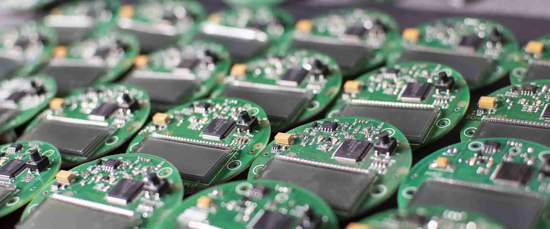
An e-card manufacturer is a company that specializes in the production of electronic cards, also known as printed circuit boards (PCBs). These are the thin, flat boards to mount and connect electronic components in various electronic devices, including smartphones, medical equipment, computers, aerospace systems, and other consumer and industrial products. Electronic card manufacturers use a combination of advanced technologies, including photolithography, etching, drilling, and soldering, to produce high-quality PCBs that meet their clients’ specific design and performance requirements.
The most competent electronic card manufacturers’ process encompasses four principal phases: module production of the smart card, body production, personalization, and card fulfillment.
Module Production
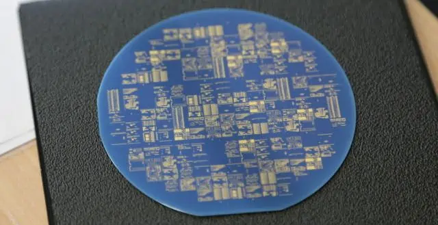
It starts with the production of the silicon wafer, where photolithography produces a silicon wafer populated with smart card chips. In ROM-based card chips, the card’s OS and some apps are engraved or burned permanently into every silicon wafer’s chip.
Wafer Initialization
It is an optional step that pre-personalizes and activates the chips while on the silicon wafer.
Dicing of the Silicon Wafer
The process splits the chips from the silicon wafer. It happens by laser cutting or mechanical sawing. However, before the cutting exercise, every wafer gets attached to an adhesive tape to avoid the movement of chips.
The process also entails the customization of the micro-connectors before electroplating with semi-precious and precious metals.
Die Bonding
It entails the application of the epoxy glue on the micro connectors pad area. After that, inline thermal curing ensues, dries, and strengthens the bonds between the micro-connector tape and the chip.
The electrical connection of the die’s contact pads and that of the micro-connector using a thin wire happens. Thermosonic bonds attach the 30um aluminum or gold wire to the pads permanently.
Techniques in thermos bonding can include wedge wire or ball bonding.
The tape then has to pass an electrical test. Here the smart chip gets powered for a simple I/O test.
Initialization of the Chip Module
All the non-marked micro-modules during the electrical test and tape inspection get initialized and pre-personalized.
Shipment to Card Body Production
It is the final step where the modules get shipped for card body production in flexible module carriers.
Body Production
In most cases, card bureaus or producers undertake this process. You must provide your smart card draft or card artwork as a customer. The stepwise process includes the following.
Customers provide their smart card artwork which then passes through the pre-press process. Here, optimization of the card draft ensures compliance with the preferred printing technique.
Once the customer approves the prototype or optimized version of their card artwork, the CTP plate production begins.
Sheet printing and inspection of the printed sheets then ensues. After that collating the diverse sheets becomes necessary. For instance, the PVC foils, clear overlay, security overlay, magnetic stripes, signature panels, and contactless antenna sheets need to follow a specific order.
Lamination becomes necessary before striping and punching the card body. After that, sim plug-in, cavity milling, and chip module implanting happen.
Quality inspection of the chip module becomes critical as you want to avoid pre-personalization and chip module testing on a faulty card.
It is the next phase of the e-card manufacturing process and makes every card distinctive from the rest.
The process involves data generation and encryption through an automated process. It then passes through a personalization system, the key’s management, and the application’s loading. However, specific process optimization and features can demand a mix of both industrial modular equipment and small specialized units.
Card Fulfillment
It is the last phase of the card manufacturing process. Mainly, it occurs through a modular machine but sometimes a mixture of automated and manual steps.
It entails the packaging of the e-card, besides shipping to the customer.
Want the Best E-Card Manufacturer?
As clearly illustrated, the manufacturing process often involves more than one company. Picking a suitable manufacturer like Rayming Technologies implies defining and understanding your card needs. Aspects like technology, competence, delivery time, affordability, and quality play a huge role.
Therefore, select the best manufacturer offering competitive prices at each manufacturing phase to ensure value for money.
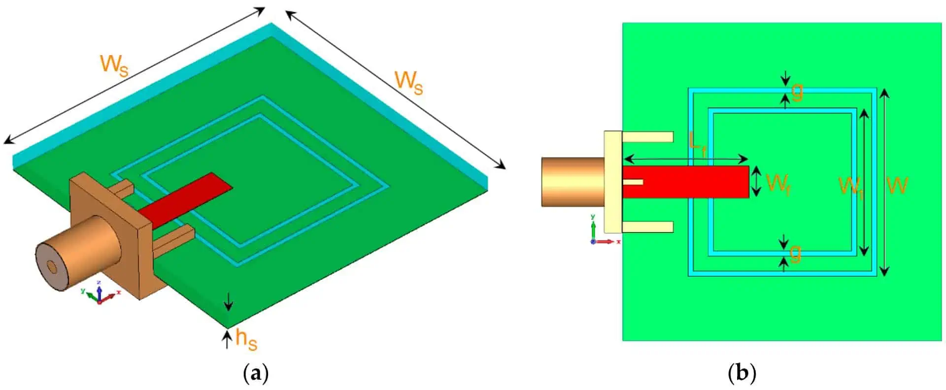
The arrival of 5G antenna technology has transformed our interactions and mobile communications with electrical engineering in the digital age. As the globe shifts toward more efficient and dependable mobile communication networks, the 5G microstrip antenna plays a crucial role in allowing the next generation of wireless communication.
5G microstrip antennas transmit and receive electromagnetic radiation through radio waves in 5G wireless communication technology networks. It is an essential component of any 5G network since it ensures reliable communication between its many features. Microstrip patch antenna technology has existed since the 1970s, but their exceptional antenna performance and low cost have made them more desirable in the 5G era.
Microstrip patch antennas are usually compact, lightweight, and low-profile, making them excellent for a MIMO system and mobile devices like smartphones and tablets. In addition, they have a cheap production cost and can be readily incorporated into existing infrastructure, which makes them a viable option for broader deployment in 5G networks.
The frequency range, polarization, and emission pattern of 5G microstrip antennas help to categorize them.
Operating Frequency
5G microstrip antennas can be low-frequency, mid-frequency, or high-frequency depending on their operating frequency band. Low-frequency 5G microstrip antennas work between 600 MHz and 1 GHz, whereas mid-frequency (center frequency) 5G microstrip antennas run between 1 GHz and 6 GHz. High-frequency 5G microstrip antennas function at frequencies greater than 6 GHz, which is sometimes the resonant frequency.
Polarization
An electromagnetic wave with linear polarization has a constant direction and amplitude of the electric field. An electromagnetic wave with circular polarization has a constant amplitude but a spinning electric field.
Emission Pattern
5G microstrip antennas can have an omnidirectional, directional, or adaptive radiation pattern. Compared to directional antennas, omnidirectional antennas emit equally in all directions. However, adaptive antennas can alter their emission pattern due to shifting environmental factors.
Patch antennas, slot antennas, printed dipole antennas, and printed monopole antennas are a few of the several varieties of 5G microstrip antennas.
Microstrip patch antenna
A flat conductive patch on a dielectric substrate makes up the microstrip patch antenna. Furthermore, microstrip patch antennas are a standard option for 5G applications because of their low profile and large antenna bandwidth, which make them suitable for a greater operating frequency in wireless communication devices.
Microstrip Slot Antenna
The slot antenna consists of a tiny slit or slot carved out of a conductive surface. Slot antennas, available in various sizes and forms, are frequently employed in applications that demand a broad antenna bandwidth and high gain.
Printed Dipole Antenna
Two conducting strips (dipoles) printed onto a dielectric substrate create a printed dipole 5G microstrip antenna. These antennas are helpful when both a large bandwidth and a low profile are necessary.
Printed Monopole Antennas
Printed monopole antennas consist of a single conducting strip, or monopole, installed on a ground plane. Applications that call for a low profile and compact construction frequently employ these antennas.
When picking a 5G microstrip antenna, performing a performance analysis and examining several aspects is essential. Among the most important considerations are the following:
Suitability
Low-frequency, mid-frequency, and high-frequency 5G microstrip antennas are available in various frequency ranges. Therefore, selecting an antenna with an appropriate operating frequency range for the intended application is essential. For instance, if the antenna functions in a low-band 5G network, a low-frequency antenna may be preferable, but a high-frequency one may be preferable for a high-band network. The higher the antenna suitability, the lower the antenna’s return loss.
Polarization:
5G microstrip antennas have either linear or circular polarization. Linear polarization is appropriate for applications requiring a constant amplitude and direction of the electric field. In contrast, circular polarization is suitable for applications requiring a constant amplitude and a revolving electric field. The appropriate polarization type should depend on the application’s unique needs.
Radiation pattern:
5G microstrip antennas can have omnidirectional, directional, or adaptive radiation patterns. Omnidirectional antennas emit equally in all directions, but directional antennas radiate more intensely in one direction. Adaptive antennas can modify their emission pattern in response to varying environmental circumstances. Therefore, choosing the optimal radiation pattern should depend on the radiation elements and the application’s requirements.
Gain
Gain measures an antenna’s ability to direct the radiated power in a particular direction. Antennas with a more significant gain can transmit a more robust signal for a specific order but may have a smaller beam width. Conversely, low-gain antennas offer a larger beamwidth, but their signal strength in a single direction may diminish. The right degree of gain should depend on the application’s unique requirements.
Dimensions
5G microstrip antennas are available in an assortment of sizes and weights. Therefore, picking an antenna compatible with the installation specifications is essential. For instance, a smaller and lightweight antenna may be preferable if the antenna is positioned in a tight location.
Durability and dependability:
5G microstrip antennas are frequently helpful in harsh conditions, such as outdoor or industrial settings, that apply MIMO antennas. Therefore, it is essential to select an antenna that is sturdy, dependable, and capable of withstanding the circumstances of the installation site.
In 5G networks, microstrip antennas are helpful in various applications. These antennas will suit the demanding needs of 5G networks due to their low profile, wide bandwidth, and high gain characteristics. Among the most important uses for 5G microstrip antennas are:
Wireless connectivity:
Widespread usage of 5G microstrip antennas enables wireless communications between various portable devices, including smartphones, tablets, and laptops. These antennas can handle the high data rates and low latencies required by 5G networks. It is easy to install them into mobile devices such as smartphones, tablets, and laptops to allow appropriate network connectivity and signal processing.
Data Transmission:
5G microstrip antennas are vital for transmitting and receiving data, audio, and video signals across 5G networks. These antennas help to accommodate a broad spectrum of 5G network frequencies and can transmit and receive signals over many kilometers. 5G networks allow high-speed data transfer and low-latency communication due to 5G microstrip antennas. Furthermore, 5G microstrip antennas accommodate multiple frequencies, making them ideal for 5G network coverage and wearable applications. 5G networks employ various low-band and high-band frequencies, which must be within the 5G network infrastructure.
Small cell networks construction:
Small cell networks are a crucial antenna element of 5G networks, as they boost capacity and coverage in densely populated locations. In addition, small cell networks frequently employ 5G microstrip antennas because they are suitable for the small form factor and low profile required by these systems.
Promoting beamforming and other cutting-edge technologies:
Microstrip antennas for 5G networks are frequently applied in conjunction with sophisticated technologies like beamforming, which can increase the performance of 5G networks by concentrating the transmission and reception of signals in specified directions. This aspect enables the adoption of sophisticated technologies such as massive MIMO systems (multiple-input, multiple-output) and complete duplex transmission, which can boost the capacity and coverage of 5G networks.
How 5G Microstrip Antennas Have Improved the Efficiency of 5G Networks
With its engineering and emerging technologies, 5G microstrip antennas have improved the performance of 5G networks. Included are:
Increased antenna Bandwidth:
The increased gain of 5G microstrip antennas enables them to deliver more significant amounts of bandwidth. In addition, this increased gain allows the transmission and reception of more data at any given moment, enhancing the network’s speed and dependability.
Signal Decongestion
The directional nature of 5G microstrip antennas enables them to give enhanced coverage in particular places. This improved coverage can assist in lessening signal congestion in some areas and enhance network performance generally.
Reduced Interference
5G microstrip antennas are less likely to create interference with other devices due to their low profile. As a result, it can assist in enhancing the network’s dependability and decreasing the likelihood of lost connections in communication devices.
Reduced Power Consumption:
Due to their diminutive size, 5G microstrip antennas require less power than conventional antennas. As a result, they can minimize the energy needed to power the network and increase radiation efficiency, making them suitable for communication technologies.
A microstrip patch antenna is an antenna that emits or receives electromagnetic waves using a conductor or dielectric patch. Due to its simple construction, low cost, and ease of production, it is one of the most often used antennas.
Components of the microstrip patch antennas
The microstrip patch antenna has several distinct elements collaborating to produce the desired radiation pattern. The components are the components of the patch, dielectric substrate, conductive ground plane, feed line, matching network, and antenna housing.
Patch element
The patch is the radiating antenna’s basic element., typically constructed of copper or aluminum. The rectangular patch is generally etched into the surface of the dielectric substrate. Typically, the length and breadth of the patch are a fraction of the target frequency’s wavelength.
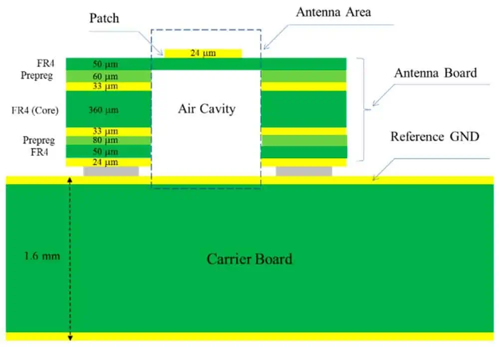
Dielectric Substrate
The dielectric substrate provides structural support and separates the patch and ground plane. Several millimeters in thickness, it often comprises either foam or plastic. The antenna’s electrical parameters depend on the substrate’s dielectric constant, which, if chosen carefully, maximizes the radiation pattern.
Conductive Ground Plane
The conductive ground plane is the component that supplies the patch with an electrical connection. It frequently comprises a metal, such as copper or aluminum, and is typically more extensive than the patch itself. The ground plane also helps to create a sizeable electrical ground for the antenna, which aids in reducing losses and enhancing radiation efficiency.
Feed Line
The feed line connects the antenna to the radio frequency source. Typically, it is a coaxial cable or a two-wire line. The feed line transmits radio frequency energy from the start to the antenna.
Matching Network
The matching network aids in impedance matching. It, therefore, matches the antenna’s impedance to the radio frequency source’s impedance. It typically consists of capacitors and inductors and helps transmit the maximum power from the start to the antenna, enhancing the device’s impedance-matching ability.
Housing
The antenna enclosure is the antenna’s last component and shields the antenna components from the surroundings. It typically consists of metal and may be either sealed or vented. The enclosure also helps decrease the unwanted radiation the antenna emits.
The following is the design methodology for microstrip patch antennas:
Substrates
A microstrip patch antenna’s substrate is the material on which the antenna is printed. The substrate should give the appropriate electrical and mechanical properties. Common microstrip patch antenna substrates include FR4, Rogers RO4350, and Polyimide (Kapton).
Due to its low price and availability, FR4 is a popular substrate. It is an epoxy-fiberglass composite with an approximate dielectric constant of 4.40 and a loss tangent of 0.02. It is rigid and appropriate for tiny antennas.
Owing to its low dielectric constant (2.2) and low loss tangent, Rogers RO4350 is a common substrate for high-frequency antennas (0.002). Additionally, it is relatively rigid, making it appropriate for compact antennas and propagation.
Polyimide is a flexible substrate frequently used for mounting big antennas on curved surfaces or large antennas on flexible substrates. The dielectric constant is 3.20, and the loss tangent is 0.002.
Antenna Design
After selecting the substrate, generating the proposed antenna design can be more manageable. Typically, the patch antenna is easy to create using a computer-aided design (CAD) tool. Patch, feed line, ground plane, and matching components make up the proposed antenna’s design. The patch is the antenna’s radiating element and is commonly configured as a square or rectangle. This connection connects the antenna to the transmitter or receiver. The ground plane is a metal sheet used to reflect radio waves. The matching components then help to tune the antenna to the appropriate resonant frequency.
Printing
We may print the antenna circuit on the substrate using several processes. The most prevalent printing processes are screen printing, photolithography, and inkjet printing.
Screen printing is a low-cost method that involves transferring a pattern onto the substrate using a screen. The screen is covered with a photosensitive emulsion, and the design is imprinted using a light source. After washing away the emulsion, the pattern is left on the substrate.
Photolithography is a more accurate printing technology that transfers a pattern onto the substrate using a photomask. The photomask is a translucent plate having a way of light-transmitting holes. The substrate is then imprinted with the design while exposed to light.
Inkjet printing is a printing method that sprays tiny droplets of an electrically conductive substance onto the substrate using a printhead. This method is suitable for small antennas due to its precision and rapidity.
Assembly
After printing the proposed antenna design onto the substrate, the antenna must be assembled. Attaching the feed line and ground plane and matching components to the substrate is required. Typically, the feed line is soldered to the substrate, whereas the ground plane and corresponding elements are bonded with epoxy or glue.
Testing
Once the antenna has been built, it must be tested to confirm the correct functionality. Typically, this entails evaluating the antenna’s radiation characteristics and impedance-matching capability. The radiation pattern measures the antenna’s efficiency, while impedance measures the antenna’s compatibility with the transmitter or receiver.
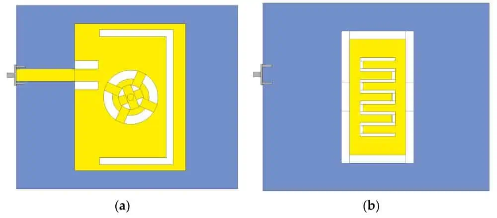
Array antenna
The phased array antenna is a form of antenna that consists of numerous radiating elements coupled via a network of electrical components. The phased array antenna’s primary function is to enhance the antenna’s beamwidth, which may be used to receive or broadcast signals in numerous directions. The phased array antenna offers a significantly larger coverage area than other antennas. Consequently, it permits substantially larger data speeds and improved signal quality.
Multiple radiating elements coupled via a network of electrical components constitute the phased array antenna’s fundamental design. The network of features enables the antenna to focus the beam in various directions. Each array unit has a phase-shift circuit for controlling the phase of the radio waves being sent or received. As a result, the antenna’s beamwidth is created by adjusting the frequency of the radio waves so that they all arrive at the same spot simultaneously.
The design of a phased array antenna can be extremely complicated, as its parts must be properly aligned and spaced for it to function correctly. For the beamwidth to be optimized, the phase of the radio waves must also be precisely regulated. To guarantee the correct operation of the designed array antenna, the phase-shift circuits for each array element must be meticulously calibrated.
Varieties of Phased Array Antennas
Linear antenna, planar antenna, and circular are the two primary phased array antennas. The linear components of linear phased array antennas are placed in a straight microstrip line. The Planar antenna is a two-dimensional array that might be circular, rectangular, or triangular in configuration. On the other hand, circular phased array antennas consist of a circular arrangement of elements.
Typically, radar, navigation, and mobile communication systems employ linear phased array antennas. However, circular phased array antennas are generally helpful in satellite communications, radio astronomy, and other applications requiring a narrower beam width.
Phased Array Antennas’ Applications
In addition to radar, navigation, communications, satellite communications, and radio astronomy, phased array antennas are used for several other purposes.
Radar:
Phased array antennas are used to identify objects using radar systems. The phased array antenna helps to scan the region to detect any items in the path of the radar beam.
Navigation Systems:
To detect the direction of a vehicle, navigation systems utilize phased array antennas. The phased array antenna scans the surrounding environment to identify the vehicle’s speed and direction.
Mobile Communications:
Phased array antennas are helpful in mobile communications systems to send and receive signals. The phased array antenna sends signals in several directions to cover a larger region.
Satellite Communications:
Phased array antennas are utilized in satellite communications systems to send signals to and from satellites. The phased array antenna broadcasts signal in numerous directions to cover a larger region. WIFI systems and Satellite transmission dishes are two practical implementation cases.
Radio Astronomy:
Phased array antennas are utilized in radio astronomy to detect radio signals emitted by distant objects. The phased array antenna searches the sky for signals to detect any that may be there.
Prospects of the 5G microstrip antenna and the array antenna
The array antenna and the microstrip antenna appear to have extremely bright futures. Research and development in the area of proposed antenna design will advance as 5G networks spread and become more common. While we expect the array antenna system to take over as the favored option for high-performance applications, we also expect the microstrip antenna to continue being a popular option for both low-cost and high-performance applications.
Additionally, we anticipate that with time, both the array antenna and the microstrip antenna will get smaller and more effective, achieving a compact form. New materials and technological developments in antennas will make it possible to create smaller, more effective designs. This improvement will make it possible to create smaller, easier-to-integrate designs for mobile devices and other tiny form factors.
Given its capacity to deliver high-performance, low-cost solutions, we look forward to seeing the microstrip and array antenna gain even more popularity over time in the 5G industry. Furthermore, more research and development in antenna design is among the key technology developments we anticipate to result from the growing popularity of 5G networks. Consequently, this will enhance the performance and capacities of both the microstrip antenna and the array antenna.
Why One Should Go for the Array Antenna Instead of the 5G Microstrip antenna
The array antenna is superior to the 5G microstrip antenna in several ways.
The gain of the array antenna is more significant than that of the microstrip antenna due to the array antenna’s numerous elements, each of which may be altered to change the antenna’s gain.
Over a microstrip antenna, the array antenna provides better directivity. This directivity is so that the array antenna may direct its radiation in a specific direction by independently adjusting each antenna element. This aspect is helpful when focusing the antenna’s energy on a particular target is crucial. In addition, the array antenna may also create several beams in various directions, which is advantageous for 5G applications since it enables the antenna to accurately guide signals in multiple directions, improving the radiation efficiency.
The array antenna is furthermore more effective than the single microstrip antenna. This is possible because the array antenna can keep a high signal-to-noise ratio throughout a broad frequency range. For 5G applications, this is crucial since the antenna must be able to send and receive data across a wide frequency range. In addition, the array antenna may also minimize signal interference, which boosts the antenna performance specifications since interference can impair transmission.
Finally, the antenna array is more dependable compared to the microstrip antenna. This dependability results from the array antenna’s capacity to preserve the signal quality over a broad frequency range, which is crucial for 5G applications since the antenna must successfully communicate across a wide frequency range. In addition, the array antenna’s ability to maintain a strong signal-to-noise ratio over a broad frequency range is also advantageous for 5G applications since it enables the antenna to broadcast and receive data more precisely.
Conclusion
Microstrip antennas are suitable for usage in 5G networks due to their many benefits. They are tiny in size, inexpensive, simple to deploy, and easily customizable to match the network’s unique requirements. However, deploying microstrip antennas in 5G networks has significant obstacles, such as their fragile construction, restricted antenna bandwidth, and directed emission pattern, enabling technologies to better their performance. On the other hand, electrical engineering and many microstrip antenna technology advancements in recent years might enhance their performance in 5G networks. Multi-band antennas, reconfigurable antennas, and active antennas are examples. In conclusion, microstrip single-patch antennas have the potential to improve the performance of 5G networks considerably, and their deployment is anticipated to increase shortly.
When deciding on the most suitable microstrip antenna for 5G applications, there are other aspects to consider. It is essential to select an antenna suited to the particular requirements.
Electronics assembly is offering a contract to assemble electronic components for another company. This is known as ECM (Electronic Contract Manufacturing) and is a service often used by OEM companies.
Instead of manufacturing complex components and motherboards, OEMs outsource their manufacturing tasks to electronic component manufacturing companies. ECM companies do not label their ingredients in any way. Instead, the component remains unbranded and bears the name of the OEM company offering the contract.
Today, many ECM companies exist, and this can make it challenging for users to determine how to choose the best electronic manufacturing services. If you need electronic manufacturing services and do not know where to start, this guide offers you everything you should know about electronic contract manufacturing services.
What Is An OEM Contract Manufacturer?
Simply put, an OEM contractor is an outsourcing company that manages the creation of equipment that the rental company cannot manufacture. OEM contract services exist in almost every industry and allow major manufacturers to expand their product or service line with minimal additional expense.
OEMs can offer significant advantages and customization options over in-house manufacturing management.
What Is the Difference Between Electronic Contract Manufacturing Services and OEM?
While electronic contract manufacturing and original equipment manufacturer for printed circuit board assembly are always misunderstood to be similar, they are different. Some of the differences between these two are seen in how electronic assemblies are conducted by expert engineers involved.
● Original Equipment Manufacturer (OEM)
OEMs design and sell parts that other companies and customers use in their products and industries. Companies, customers, and industries that buy OEM parts are value-added resellers (VAR) who specialize in a particular electronic product, galvanized steel or offer design assistance for those who build to print.
OEMs and VARs, who are customers or industries, work together to ensure quality conformal coating of lead time and other electro-mechanical or industrial tools used in the assembly process.
● Contract Manufacturer (CM)
Small businesses can hire other companies or contract manufacturers (CMs) with quality certifications to manufacture their products using cutting-edge technology for fulfillment services while ensuring functional testing when they want to harness assemblies before the surface mount is done in electronics manufacturing
These manufacturers ensure rapid prototyping for electronic assembly, PCB assembly, circuit board assembly, and other contract manufacturing services like electro-mechanical assemblies; they offer seamless deliveries of wire harnesses and electronic products for commercial industries.
Any company specializing in PCB assembly, electro-mechanical assembly solutions, box builds, consumer electronics, sophisticated electronic products, wire harnesses, box build assembly, and mixed technology can use contract manufacturing. The services these original equipment manufacturers offer guarantee high-quality products and customer satisfaction for all box builds.
Other companies that can use electronic manufacturing, asides from those that harness assemblies for box builds, include:
Parts require large capital investment in equipment, such as metal stamping, machining, aerospace, automotive, industrial, and distribution equipment.
Parts require highly specialized manufacturing expertise, such as printed circuit board assembly.
Sometimes, you may wonder why people opt for electronic contract manufacturing for printed circuit board assembly or packaging control instead of considering other options for customers. Yes, the other packaging or control options may be cheaper, but the benefits of electronics manufacturing and the electronic assembly project are numerous.
1. Reduce Capital Investment And Risk
Building a factory or renovating an aerospace or industrial production line on specifications requires a large capital investment and many other resources. In addition to capital, the following resources will be required:
Construction management
Production engineering
aerospace and industrial engineering
Sources of financial analysis
Project management
In addition to the resources mentioned above, the automotive project will take some time, depending on its specifications. Investing large resources may be wise to create a stable and low-risk product with great ability. Contract manufacturing makes much sense for lesser-known and more speculative automotive products.
2. Flexibility
Running your factory requires an investment of capital and human resources with the right ability for maximum delivery or prototyping services and quality electro-mechanical services. Once that commitment is made, change is very difficult to make. It is very difficult to change:
No business wants to deal with the headache of changing factories. When you contract with a manufacturer, you don’t have to worry about internal changes they make. The electronic contract manufacturer is responsible for fulfilling its part of the contract with you. This is when they can devote their time and energy to the core of their business, such as sales.
Even if your company has enough capital to build a factory, the cost of the final product still needs to be determined. If cost overruns occur during construction or production, labor costs are higher than anticipated; this will increase the cost of the product. Production schedules are also at risk with any new project. Several elements can negatively affect production time:
Construction delays
Delays in the delivery and installation of production equipment
Selection and training of new production workers
If you want to know exactly how much your product will cost and when it will be delivered, hire a proven contract manufacturer. They will calculate the figure for you and specify the cost and delivery time in the contract.
4. Experience and Expertise
There is a popular saying, “Do what your business does best and outsource the rest.” Is manufacturing not your company’s forte? Therefore, it makes sense to outsource to an experienced contract manufacturer. A manufacturing company needs time to solve problems before it becomes good and streamlined as a stable manufacturer. Its:
Impact on your business results
Achieve the quality of your product
If you want to make a good first impression on your clients, choose a qualified electronic contract manufacturer who:
Has experience in manufacturing your product or a similar product
Can start production quickly
Produce quality products
Employ qualified employees
Experienced contractors of PCB assembly know the ins and outs of electronics manufacturing. Instead of reinventing the wheel, most companies are better off hiring existing and experienced manufacturers for PCB assembly or harness assemblies of quality electro-mechanical prototyping.
Advantages of OEM
Whether it is for printed circuit boards assembly solutions, cable assemblies, circuit boards restructuring, electro-mechanical assembly solutions, or electronic manufacturing services, here are some of the benefits of OEM:
Using an OEM, you can customize the service or product as long as it is technically possible.
As long as you have the right contract and cover. You own the intellectual property.
You will have an exclusive product in the market.
Disadvantages of OEM
It is not always enough to focus on the capabilities and benefits of OEM alone; you must note some of its advantages and include:
Buyers will have to cover the costs of tooling and molding, which can be very high.
Creating molds and making new tools takes at least a month, usually longer.
The Benefit of Using OEM Contract Manufacturing
In the medical line, contract manufacturing presents an opportunity that helps medical companies to keep up with the rapid technological development of medical devices and bring new and necessary products to market with efficiency, speed, and increased profitability.
● Specialization
The medical device OEM industry includes a wide range of products that need electronic contract manufacturing, from basic patient-operated devices. These devices range from small enough to be held in hand to large and complex electronic consoles designed for physicians and healthcare professionals within the hospital or office settings. With the right contract manufacturing services for PCB assembly, quality electronics and services can be made available in the medical industry.
● Scale
Due to specialization, industries offering contract manufacturing to established companies benefit from economies of scale in quality labor, materials, and services. This allows contract manufacturers often to purchase bulk materials and services at discounted prices, and delivery of finished and specialized parts is done quickly.
● Savings
OEM electronic contract manufacturers’ dual specialization and economies of scale provide overall cost savings for medical device OEMs. Not only do they save on labor, materials, and equipment, but they also reduce the time it takes to get from concept to finished product.
How to Choose the Right Contract Manufacturing Partner
If you’re looking for a contract manufacturing service for the partnership to optimize your production, here are some tips to help you search. Good CM:
Understand customer, statutory and regulatory requirements
Meet and exceed these expectations without compromise
Deliver goods without defects, on time, every time
Regardless of the type or complexity of your relationship, your contract manufacturer should still be concerned with quality service and customer satisfaction.
Conclusion
Electronics contract manufacturing is a business model where OEMs hire EMS companies to complete hardware construction. Both parties benefit from creating an electronic contract, which is why seeking the best, like those offered by Rayming PCB assembly, which you can access when you click here.
If radio signals and waves were tangible and visible, then it will be impossible to move between two ends of your apartment without tripping.
Now, what are those things that keep the signals from coming in contact or crossing? How is it possible to pick up your phone without this signal interfering with your laptop’s WiFi connection and cause some disruptions? This disruption is what we refer to as electromagnetic interference.
The truth is that we hardly see them due to an efficient electromagnetic interference protection or shielding, which is also called EMI protection. Before we go into details, we will explain what EMI means, what EMI protection means, and the types.
Please continue reading to comprehend all you should know regarding EMI protection as well as those materials that gives these signals a proper check.
EMI, described simply, involves the transmitting of undesirable electromagnetic radiation into an electronic or electrical device. The signals interfere with the operation of the device, which could cause great harm. Also, EMI can come up or originate from different sources, which could be both man-made and natural. EMI takes place anytime one source disturbs or disrupts the signal of another source.
Engineers also call it RFI, which means radio frequency interference. Although the above instance explains a negative result of the EMI, this form of interference could lead to more issues than make you mis your bars on some favorite songs.
In addition, EMI shouldn’t even emanate from a specific outside source. Also, internal EMI, where one of the components of the device generates interference in a different component, is known as a usual source of issues. Upstream issues having the conditioning and quality of different power sources are also well-known common culprits. Also, these internal EMI types working hand in hand can cause real issues for device builders and designers.
As if the sources haven’t caused enough issues, nature itself could also generate EMI. Some atmospheric phenomena such as solar systems and thunderstorms are all natural emitters of an electromagnetic radiation. Also, they could have some negative effects on the electrical devices.
What is EMI Protection?
With all the issues caused by EMI, EMI protection is very important. Our devices require some protection and safety from picking the wrong signals up, and security for choosing the appropriate and right signals. With EMI protection, you will be able to increase this success.
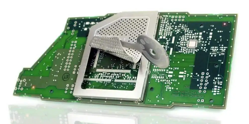
EMI protection involves a material that stops electromagnetic interference. This is made up of a specific metallic screen, which helps in absorbing any interference that has been transmitted via air. In addition, EMI protection exists to help protect your device’s electronics.
Furthermore, as these signals get to your device, this screen goes ahead to absorb them. This causes a current in its body. This current is then absorbed by a ground connection. This EMI shield helps in absorbing any transmitted signals even before they get to the device’s sensitive circuits. It also helps in ensuring the cleanliness of the protected signal.
One important example of why the EMI shield is very necessary is your Smartphone. You have different intricate, sensitive, electronics working at one to ensure that the display says exactly what it is saying. With an EMI shield, it helps in preventing random waves and signals form frying sensitive electronics. Devices like key fobs and Wi-Fi routers require the ability of transmitting the RF signals wirelessly.
Metal enclosures, as well as other enclosures blocking EMI could also block any transmission relied on by these devices. A wise and effective choice for all these applications is polycarbonate enclosures. Gaps or seams that are not well secured can compromise the performance of the enclosure shielding.
Even the small apertures present in any enclosure can serve as antennas, which allows the entering or leaving of EM radiation. To fight this, designers of enclosures will specify the enclosures with continual body designs.
Types of EMI
Narrow-band EMI
This usually happens to radios, TV stations, as well as mobile phones. This is because it happens over a specific discrete frequency. Anytime signals cross, devices malfunction. The customer can simply tune out that disruption, which won’t bring any damage to the equipment.
Broadband EMI
This takes place over a broader spectrum because it occupies a massive part of the electromagnetic spectrum. Broadband EMI is a form of EMI which can cause maximum harm to devices. Also, you notice this form of interference at its peak while using a device featuring a specific digital data link.
Furthermore, something as easy as a motor’s worn brush can lead to EMI. Also, a fluorescent light having defects implies EMI. This similar interference could appear from a jet engine’s igniter. Defects present in a power line will lead to interference too.
Taking a look at each case mentioned above, the devices you are trying to utilize can have varying transmitted frequencies, blend them up, after which they are sent out over a very broad spectrum.
EMI or Electromagnetic interference is a disturbance that is created through the changes in voltages and currents that result due to three main sources.
Natural EMI
Some natural events happening in space or on earth could cause natural EMI. Humans have no hand in the creation of EMI. This occurs as a result of weather changes like rain, snowstorms, thunderstorms, etc. Also, some natural sources such as cosmic noise and solar radiation also create EMI. In addition, the natural EMI has an effect on older equipment and to a larger extent on RF communication. Notably, the modern equipment isn’t just affected a little by the natural EMI in contrast to the human made EMI.
Human-made EMI
All the electrical devices manufactured usually release EMI that are human-made. This interference is usually caused whenever two signals come near or whenever many signals meet themselves at just one frequency. All this helps in obstructing the devices’ operation whenever they have a contact with an EMI.
Also, this EMI is majorly seen in devices such as igniters, generators, power lines, radio transmitters, electric motors, phones, etc. Such devices and equipment are usually known to result in dangerous EMI levels.
Internal or Inherent EMI
For inherent EMI, this electromagnetic energy that is released from a device can cause its breakdown. That noise caused internally or inside is from the electron’s thermal agitation which is moving through its circuit resistor.
How to Reduce or Eliminate EMI
Shielding
This is the most preferred way for containing coupling or radiation in victim or source devices. Usually, it is made up of encasing its circuit in a well sealed enclosure, like a metallic box. Furthermore, shielding is important because it helps in reflecting electromagnetic waves in the enclosure as well as absorbs waves which aren’t reflected.
For majority of cases, a very little radiation somehow penetrates the shield, if this shield isn’t very thick. Practically common metals will serve this shielding purpose (e.g. aluminum, steel, and copper).
Filtering
This is a direct way of eliminating any undesirable signals, and for this case, passive filters function effectively, and they’re useful in majority of new equipment in minimizing EMI. Also, filtering usually begins with the AC line filter, which stops the entering of bad signals into the powered circuits or power supply. It also stops the addition of the internal signals to the AC line.
Furthermore, filtering is usually used with connectors and cables on the lines out of and into a circuit, and there are special connectors which have low-pass built-in filters where their major function is softening the digital waveforms to help in increasing the fall and rise tomes as well as reduce the harmonic generation, with respect to electronic design.
Grounding
This has to do with establishing of electrically conductive paths in-between an electronic or electrical element of any system as well as a reference point, according to the DAU. Also, it could indicate electrical connections that are created to Earth.
It is very crucial to understand the need for EMI protection for numerous reasons. As regards the development side of the spectrum, the product of a company is only as effective as it functions once it gets to the end user. For instance, if an electronic device malfunctions continuously, that is a bad indication for the company.
Developers are experiencing greater challenges as regards combating EML. This is because faster operating electronics makes it difficult to manage interference. However, the inability of engineers and designers to account for EMI will most likely result in a faulty product.
Furthermore, workers who often handle large amounts of big data could find it difficult to handle EMI as interference can disrupt the mediums through which they gain access to such information. EMI is something that needs serious attention, both from the workplace environment side and product development side.
EMI protection is very important irrespective of the product. In as much as conductive silicones and gaskets are an ideal option in terms of product, another consideration may be the right type of window film to shield office locations from interference.
Also, EMI protection is crucial in shielding sensitive electronic designs from external signals and as well preventing the interference of stronger signals with nearby electronics. With a PCB design checklist, you can figure out what needs protection and how to achieve it.
Electromagnetic interference impacts sensitive electronics and has an impact in different sectors, including industrial electronics, and mission-critical military electronics. Therefore, it is important to ensure that the electronic systems get enough protection against EMI.
Common Tools and Techniques in EMI Protection
emi emc shielding materials
EMI protection simply involves the integration of different countermeasures to shield electronic and electrical devices from EMI. There are methods of EMI protection, this includes:
The majority of electrical device designers will build an enclosure box made from material like steel or aluminum. These metals feature natural EMI shielding. Also, a well constructed metal enclosure can retain and redirect the interruption instead of allowing it to get to the device inside. Silver, copper, aluminum, and other kinds of steel are materials widely integrated due to their natural resistance to EMI.
Installing an electronic enclosure having an EMI-shielded gasket reduce or prevent EMI in a device. Also, these gaskets comprise standard materials such as neoprene. However, they comprise conductive metallic linings such as wire mesh that transform the gasket into a conductive barrier that fights EMI.
Another great alternative for including EMI resistance in an enclosure is the use of conductive spray coatings. Also, these coatings feature metals such as nickel or copper in a spray-on format. Therefore, one could apply it to non-conductive materials and as such, offering a great way to include EMI resistance to various types of device enclosure.
EMI-shielded cables can combat various EMI-transferring properties features by electrical cables. Furthermore, cables can generate and receive EMI. Shielded cables can as well minimize vulnerability to both. Therefore, this makes them an effective and crucial part of the solutions toolbox that helps to enhance the EMI resistance of a device.
The majority of device designers usually include electronic filter circuits to the most crucial components of a device to minimize their susceptibility to EMI. There are several filter designs available. Filters are a popular and versatile choice for regulating EMI in different devices. This is because you can calibrate them to accept particular frequencies and reject others.
When governmental bodies realized the importance of EMI, they enforced equipment compatibility via regulations. For example, IEC 61000-4, standardizes test methods. The relevant sections to this discussion are IEC 61000-4-5 for high-energy transients (SURGE), IEC 61000-4-4 for fast transients (FTB), and IEC 61000-4-2 for electrostatic discharge (ESD). These are test methods that depend on only realistic models for electrical noise.
Before the application of protective elements, you need to consider these rules:
Consider EMI protection while designing the circuit, not after designing the circuit.
Ensure you block interruptions that are near to the source, do this before they reach the equipment; you can redirect them to ground.
Locate all sections that can expose to EMI disturbance from sensitive circuitry.
Since signal circuitry can’t resist kilovolt-level voltages, you need to exclude these disturbances from the input, convert to current, and heat them. Isolation is of great importance for the occurrence of high ground-loop currents and longer lines in industrial systems.
Also, an ESD current pulse with 30A peak may only generate tens of millivolts of resistive voltage drop. Skin effect is important at these high frequencies as it helps to dramatically increase wire resistance by ensuring current flows within microns of the conductor surface. You need a large surface area for ground connections to counteract this effect. This helps in maintaining low resistance.
Common EMI Protection Components
Gas arrestor
A Gas arrestor is a type of dish-shaped capacitor that contains gas, most especially neon. If there is an voltage in excess of ~100V, this will create a plasma that reduces the voltage at low levels. Also, gas arrestors retain high-level transients. However, they are not ideal for fast transients since the emergence of plasma is time-consuming. They are also not ideal for mains protection. Gas arrestors are very difficult to utilize with low-source impedances.
Varistor
Varistor is an arrestor that comprises metal oxide (mostly zinc). This component looks like a tablet having two connectors, one on each side. It has similar characteristics with a zener diode. Therefore, it reacts much faster than the gas arrestor. However, it possesses high leakage currents particularly when the signal reaches the clamping voltage.
Capacitors
Capacitors are the most crucial protective component. The important properties of capacitors include voltage capability, inductance, equivalent series resistance (ESR), and high-current capability. Placing the capacitors in the right location in the layout helps to reduce EMI. When capacitors are properly used, they usually create a high-frequency ground to create a lowpass filter.
Series resistors
Series resistors are important and low cost protective components. These EMI protection components can replace more expensive components if properly selected based on power dissipation and resistance.
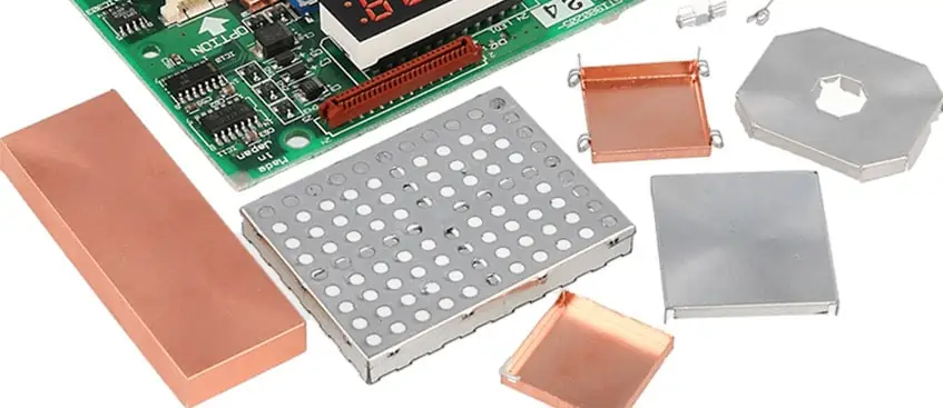
EMI Protection Materials
There are different materials for EMI protection. These materials should feature some particular electrical and magnetic properties. Also, they should retain or discharge the radiation generated by communication equipment and electronic devices. Also, the absorption shield type is more effective as it becomes safe for the environment. Most times, non-intrusive materials are used for EMI protection.
Pre-Tin Plated Steel
This material usually less expensive than the other type of metals integrated in EMI protection. However, it is a perfect option for lower frequencies, particularly in the kHz range. In particular, carbon steel, offers low-frequency shielding characteristics that other metal options don’t offer. Also, it shields the steel from any form of corrosion.
Copper Alloy 770 / Nickel Silver
This is also commonly referred to as alloy 770. Copper alloy 770 comprises nickel, Zinc, and copper. It is often used due to its resistance to corrosion. Furthermore, copper alloy 770 is a perfect option for EMI shield used for mid kHz range up into GHz. Copper alloy features a permeability of 1. This shows that it is ideal with MRI machinery.
Copper
Copper is a totally different material. It is the most reliable metal used for EMI protection because it reduces both electrical and magnetic waves. Also, copper is widely available. You can find it anywhere EMI protection is necessary from hospital equipment to basic consumer appliances.
Copper is more expensive than pre-tin plated steel or copper alloy 770. However, it has a greater rate of conductivity. This makes it a very effective option for an EMI shield.
Aluminum
Due to high conductivity and its strength-to-weight ratio, this material can function well as an EMI protection material. Aluminum has almost 60% of conductivity.
The increasing use and demand for electronic devices and mobile wireless communications has made manufacturers to seek for ways to shield their products from interruption.
The automotive industry as a whole is experiencing a new wave of autonomous cars and electric vehicles across the globe. Also, these vehicles come with sophisticated features such as hands-free systems, touchscreen systems , onboard GPS navigation systems, and Bluetooth. The electronics present in these vehicles resulted in some challenges when combating EMI. Therefore, there is a higher demand for EMI shielding in autonomous and electronic vehicles.
Telecommunications
The telecommunications industry is another industry experience rapid growth globally with the rising adoption of smartphones and the introduction of new and sophisticated technologies such as 5G. Also, the towers and components utilized require effective protection to enable smooth transfer of data. Furthermore, there is high requirement for EMI shielding in the telecommunication sector. This requirement will increase even further in the future.
Defence
The defence industry needs a high level of EMI protection in its operation. EMI shielding is now one of the relevant technologies in the military sector. It offers protection to trucks, drones, control panels, and helicopters. This helps to safeguard sensitive components. Also, the quality of EMI shielding is very important in fighting against strong disruptions.
Aerospace
It has become crucial to minimize the vulnerability of aerospace equipment to EMI. When aerospace equipment experiences electromagnetic interference, it must not generate radiation that impedes operations. As a result, the integration of EMI filtering materials has rapidly increased in the aerospace industry. Also, the increasing number of space exploration missions is a reason.
Conclusion
By now, you should understand what EMI protection is all about. We don’t live in a perfect world. Therefore, our electronic and electrical devices can become susceptible to negative impact by EMI. We know have a clear understanding of how EMI affects electronic and electrical devices. Also, we now know the measures to adopt to help prevent or reduce EMI. We have, therefore, created guidelines to help us control acceptable limits of EMI. Furthermore, modern technology has offered various options made from various materials to prevent unwanted interference.
The magnitude of the domain of electronics and their production is much higher. However, there is a factor of outsourcing these products, pertinent services, and the electronics counterparts that are also linked with the fabrication and production of printed circuit boards. There have been several reports that show that the industry of electronics has much capacity to generate bigger revenue in forthcoming years.
There is no doubt that technology and its demand in the market are escalating at a rapid pace. It means there are more opportunities in this domain that need to be explored yet. There is still a need for agencies that leverage technology to offer solutions that address consumer-based problems and daily issues.
In this case, electronic manufacturing services make their way into providing feasibility to consumers. In this guide, we will discover some important aspects of such services in detail.
Electronics manufacturing is related to the production of electronics on small and large scales as per the demands of consumers in the market. The production of electronics is a crucial factor that determines the smooth flow of this service to a large extent.
It also includes the assembling of electronics like printed circuit boards as well. Most associates of electronic manufacturing services are those who specialize in fabrication. In this way, huge and important contracts always exist in this field.
It is important to understand the responsibilities of these agencies and manufacturers. These companies offer after-services which are crucial for the consumers. These offer other services like designing, prototyping, and inspecting the electronics being produced.
There is a wide range of suppliers linked with this field that offer flawless electronics and their components. Different phases of the process these seasoned manufacturers have to follow for non-faulty production. Two prominent portions of this process are there. First is the one which covers electronic products, and second is the electronic parts of these devices.
Expected Services from Electronic contract manufacturing company
Following is the detail of the services offered by an electronics manufacturing company.
1. PCB Assembling and custom electronic product development process
There are two major techniques to develop printed circuit boards. One is by using the through-hole technique, and the second is by using surface mount technology. Both methods are different and have their own advantages and downsides.
The SMT includes small to big circuit parts like capacitors, resistors, and transistors, which are attached to the upper surface of the circuits with the help of a solder paste.
After that, proper wiring and routing take place to administer power through the entire circuit. However, the through-hole method is time-consuming, and there are more chances of human error in this technique. Due to this reason, SMT is a viable method useful in upcoming electronic launches and different gadgets related to this field.
2. Cable Assembly factory and manufacturing capabilities
Cable assembly service is another major factor of electronic manufacturing service. Different products also require cable assembling due to the inclusion of filaments, wires, and cables in their structures. Another type is called harsh-environment cable assembly, including harnesses cable assembly and mechanical assembly.
These are some major types and have major applications in different domains for clients and buyers. There are three basic services offered by a seasoned and experienced service provider. These include the production of electronics, an inspection of these products, and engineering-based tasks.
The designs require manual soldering for a flawless finish. These services need to be offered by a certified and authorized service provider. The steps of injecting and molding are also essential to consider. These help in producing one component at a time but more than one production material is used for its development.
The skill of a producer is often evaluated and assessed by its molding technique by different buyers and clients. An important way to garner a strong relationship with the consumers on all counts.
This is another important service related to EMS. There are different types of electronics for this service, such as box builds. There are also several designs of tech-based enclosures produced by the same technique. Metals like steel, iron, and aluminum and non-metals like plastics are important raw materials for this kind of production. There is a special team for this assembly. Their responsibilities also include electromechanical assembly. Additional services are functional inspection, 3d modeling, refining, and encapsulation. Furthermore, packaging, shipping, and customization are also major services of service providers.
4. Contract and Electronic Design
Contract design is a service that is in high demand from the consumer end. Different companies which lack these contract designers need to outsource to external contract designers. These are engineers in this domain and help clients with different projects. These offer services of DFX analysis, which is an affordable technique.
Validation and inspection are also important to approve the spotless designs of the electronics and products. Environmental testing, software deployment, and inspection are all such services in this field. These services should be documented, and there must be tangible proof of the purchase of these services with the clients.
There are also different experts that deal with the regulation and management of the materials. Additional services are circuit simulation, costing exercises, prototyping, product reviewing, and final inspection.
Applications Of Custom Design Electronic Manufacturing Services
1. Telecom
Telecom and data processing are two intense applications of EMS. Knowledge and education about these domains are important to keep the technical complications at bay. The network-based system is also essential to consider in this aspect of telecom.
2. Aerospace and Defence
Aerospace and defense are also executing EMS to a large extent. There should be no negligence in the inspection of the equipment. It also works in fluctuating climates. EMS is useful for the process of electrification of aircraft that are useable in the military and defense.
3. Industrial
Industrial operations are all relying on electronic manufacturing services. This service is for maintaining the entire lifecycle of the products being useful in different sectors of the globe. Scope and specification are important terms related to the industrial application of EMS. Additional services are prototype development, inspection, and last-minute assembling as well.
4. Medical
The medical domain also looks up to these services. These are reliable for executing flawless production methods and other techniques. They are able to maintain the quality benchmark as well. The experience of these service providers is also important to consider being a client since customer satisfaction should be the first goal of every service related to this field.
Challenges & Future Of Custom Electronic Manufacturing Services
Commercial services like electronics contract production are always fluctuating. This is not only beneficial but also has some major challenges to face upfront. However, this sector has a bright future with convincing opportunities for everyone. It is important to dig deeper into the challenges confronted by this domain to have a better knowledge about it in all the aspects possible.
The Challenges Of Custom Electronic Manufacturing Services
These problems that EMS has been facing for many years are not recent and unique. Instead, these have been growing in size due to the lack of solutions provided to alleviate these problems. There are also different solutions that can help reduce these challenges for every associate of this domain. One prominent factor is the service charges.
Custom electronics are not for halting earlier; instead, these keep varying from one service to the other. Another challenge is business rivalry and competition, which can be a nuisance for many budding service providers. The dumping of waste is also a big challenge in the EMS domain.
The waste materials are directly disposing into the environment, which is causing serious and alarming environmental threats. Some issues are related to traceability and compliance. Another problem is automation, and there have been several reports that show the complications related to automation.
The investment is made in the infrastructure, and the support system is on the verge of disruption due to ignorance of the solutions offered to address this challenge. Different industries like medical and aerospace are being compromised due to this one issue. The product lifecycle and its issues are another major downside of this domain.
The management system is also important in regulating the product lifecycle, which cannot be ignored. All these challenges can either have a positive or negative impact as per the fashion of regulation and execution from the service providers.
The Future Of Custom Electronic Manufacturing Services
The future of EMS lies in the novelty of solutions and new inventions in terms of automation. So that This can create a healthy influence on the robotics industry and other relevant domains; in this way, this industry will become simpler, and everyone will have equal access. The future development of the EMS also relies on environment-friendly solutions.
It is important to keep in mind that the progress and propagation of technology must not harm the environment at all. Future tech-based innovations would consume less energy, thus regulating energy consumption on all counts. If this happens, there will be more admirers of this industry in the forthcoming years. There will be more businesses in this sector, and the products will be more vigilant in energy usage.
Final Thoughts
The fact that EMS is the future of different domains around the world cannot be more accentuated. It is the same influence of EMS on the field of engineering. In this way, there will be more development in the field of technology.
Owing to this fact, this post contains all the sides of the picture to give you a vivid knowledge about the pros and cons of the EMS and its significance in different domains of the world and for different clients.
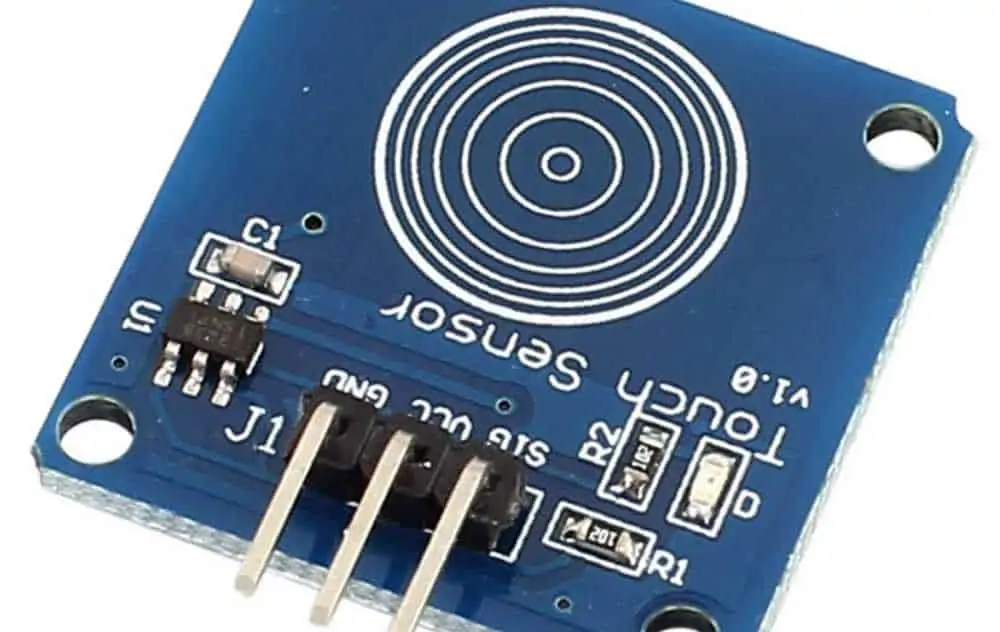
With the introduction of new technologies, the need for efficient and precise touch sensing in the printed circuit board (PCB) manufacture has increased. Over the past few decades, PCB manufacturing has advanced significantly. Despite the continued widespread use of conventional production techniques, PCB fabrication has received a technological boost.
Touch-sensing technology is one of the most intriguing recent breakthroughs in this area. With the help of this technology, a PCB may be easier to produce with a better degree of accuracy and precision by being able to detect slight differences in its surface. In this article, we’ll examine touch sensing’s application to PCB manufacture and how it might raise the overall standard of the final product. We will go through the many kinds of touch-sensing technologies that are out there, the advantages of employing them, and the difficulties involved in integrating them into the manufacturing process. We’ll also look at a few of this technology’s applications and how they might help make PCBs more dependable and effective.
Touch sensing refers to a class of technologies that allows machines and other devices to recognize when they have come into contact with an object. Robotics, automation, and smart home systems are examples using this form of sense. In addition, touch sensing helps to identify when a person has made actual contact with an object. For example, it may determine whether or not a thing is there, its dimensions and form, and the intensity of any touch. It can also pick up on changes in temperature and motion. There are two primary categories of touch-sensing technology:
Active touch sensing
Passive touch sensing
Active Touch Sensing
Active touch sensing utilizes mechanical or electrical signals to assess an item’s physical features or forces that would be difficult or impossible to detect in any other way. It is essential to comprehend the physical world around us and manage the environment. Active touch sensing employs active sensing techniques to measure an object’s or surface’s characteristics. It is a type of non-destructive testing that enable us to learn more about how materials, parts, and products’ surfaces behave.
Types of Active touch sensing
Different types of active touch sensing detect various aspects and perform multiple functions. The following are the most prevalent of these types:
Force Sensing:
It is a type of active touch sensing that detects the force exerted on a surface or object. The characteristics of a surface, such as its stiffness, flexibility, or elasticity, may be easy to measure via force sensing. To identify items or dangers, force sensing may also help to determine whether a surface can withstand a given threshold of force. In industrial automation, force sensing helps to determine if a tool or component is in the correct position.
Pressure Sensing:
This sort of active touch sensing senses the pressure exerted on a surface. For example, the characteristics of a PCB, such as its hardness, density, or compressibility, may be easy to analyze via pressure sensing. To identify items or dangers, pressure sensing may also help to determine whether a surface has attained a given threshold of pressure. When a tool or component is in the correct position, industrial automation can employ pressure sensing to determine this.
Torque Sensing:
A form of active touch sensing, torque sensing calculates the torque imparted to a surface. The characteristics of a surface, such as its resistance to rotation or its capacity to withstand torsional loads, can be measured via torque sensing. To identify items or dangers, torque sensing may also help to determine whether a surface has received a given threshold of torque. In industrial automation, torque sensing can aid in determining if a tool or component is in the correct position.
Moment Sensing:
A form of active touch sensing, moment sensing gauges the force applied to a surface. Moment sensing can help us measure a surface’s characteristics like torque, stiffness, or bending resistance. It may also help determine whether a surface has experienced a given threshold of the moment, which helps spot things or dangers. Moment sensing is a technique that may be used in industrial automation to determine whether a tool or component is in the correct position.
Vibration Sensing:
Vibration sensing is a technique that gauges surface vibration. The characteristics of a surface, such as its resonance frequency or natural frequency, may be measured via vibration sensing. Vibration sensing can also help to identify items or dangers when a surface has received vibrations that meet a predetermined threshold. For example, when a tool or component has sat in its correct position, industrial automation can employ vibration sensing to determine this.
Passive touch sensing is a technique that employs mechanical or electrical sensors instead of an external power source to detect contact with an item. In addition, this method uses many sensing techniques to detect and quantify physical signals such as pressure, temperature, and vibration. It is a crucial tool for the human-machine interface since it allows for a natural and intuitive approach to communicating with digital systems.
Types of Passive touch sensing
The following are some of the most frequent passive touch-sensing methods:
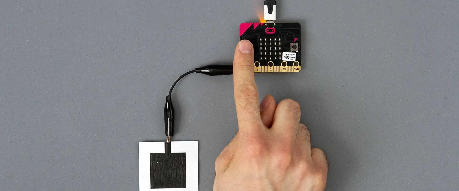
Resistive Touch Sensing:
Two thin layers of material separated by an insulating layer are useful for resistive touch sensing. The two layers come into contact and connect when subjected to pressure. This link helps to identify a touch’s presence. This touch sensing is often applicable in touch displays, game consoles, and other consumer electronics.
Capacitive Touch Sensing:
Capacitive touch sensing employs an insulated, low-voltage electric field-charged surface. The electric field is interrupted when a surface is touched, enabling the gadget to detect the contact. This touch sensing is typically helpful in medical applications, such as blood pressure monitors, touch displays, and other consumer devices.
Infrared Touch Sensing:
To detect the existence of a touch, infrared touch sensing employs an array of infrared LEDs and photodetectors. When a finger or item contacts the surface, it blocks a portion of the infrared light detected by photodetectors. This touch-sensing technique is frequently applicable in huge touch panels, video game consoles, and other consumer devices.
Ultrasonic Touch Sensing:
To detect a touch, ultrasonic touch sensing employs an array of ultrasonic transducers. When an object comes into contact with the surface, it reflects part of the ultrasonic waves, which are then detectable by the transducers. This touch sensing is often helpful in medical applications, such as blood pressure monitors and consumer electronics.
Piezoelectric Touch Sensing:
A tiny material wafer is attached to an electrode and coupled to a power source for piezoelectric touch sensing. The wafer creates a small electrical charge when subjected to pressure, which the gadget detects. This touch sensing is often helpful for medical applications, such as blood pressure monitors and consumer electronics.
Typical Applications of Touch Sensing
Touch Sensing PCB
Medical Devices
Touch-sensing technology can be helpful in medical equipment such as prostheses and assistive devices. For instance, it may be excellent in prosthetic limbs to sense pressure and strain, allowing for more precise control by the user. In addition, it helps to measure the skin’s temperature, providing a more accurate health assessment of the user. Finally, it helps to assess the pressure of the user’s grip in assistive devices such as wheelchairs and walking frames, allowing for more precise device control.
Consumer Electronics
In addition to smartphones, tablets, and wearables, touch-sensing technology may also apply to consumer electronics. For instance, it can detect the user’s touch, enabling the gadget to reply correctly. It may correspondingly apply to gaming gadgets to study the user’s movements, allowing the device to respond appropriately. Wearables may help to measure the user’s heart rate, enabling the device to deliver more precise health information.
Automation in Industry
Touch sensing technology can also implement industrial automation applications, such as robotic arms and assembly lines. For example, it can detect the location and pressure of the robot arm, allowing for more precise control over the arm’s movement. Additionally, it may help to detect the location and pressure of pieces on a production line, enabling more efficient production operations.
Automotive applications like in-vehicle infotainment systems may utilize touch-sensing technology. It can sense the user’s touch, enabling the system to react correctly. It may also help detect the user’s motions, allowing the system to understand the user’s orders more precisely. In addition, it may help assess the user’s grip pressure, allowing the system to respond appropriately.
Automation of Buildings
Touch-sensing technology can also implement building automation applications, such as door locks and security systems. In addition, touch-sensing is also applicable in lifts and conveyors. For example, the system detects that the user has gone inside the elevator, closes the door automatically, and initiates a motion in the specified direction. Similarly, it determines the correct floor using sensors and stops on arrival.
Sports
Sports applications like golf clubs and tennis racquets can also utilize touch-sensing technology. For example, it may detect the user’s grip, enabling the gadget to respond accordingly. Additionally, it can measure the force of the user’s swing, allowing for more precise evaluations of the user’s performance. Additionally, it may monitor the acceleration of the user’s swing, enabling more exact measures of the user’s power.
Background and Introduction of Touch Sensing in PCB Production
Since the first touch-sensitive gadgets were created in the late 1950s and early 1960s, touch sensing has been around. These devices were most helpful in the medical sector, such as blood pressure and heart rate monitoring. However, the technology has evolved and developed to be applicable in several other applications.
The first touch-sensitive switches appeared in consumer devices in the 1970s. Notably, these switches were standard in video games and other interactive devices. Later in the 1980s, touch-sensitive screens started appearing in various gadgets, including digital watches and calculators. Touch-sensitive displays were applicable in mobile phones and other portable devices by the middle of the 1990s. In the late 1990s, touch sensing in PCB manufacturing first gained traction. Initially, this technology was for industrial uses, including the management of machinery and robots. However, consumer electronics are among the many applications for which the technology has modified and developed throughout time.
Furthermore, to provide touch sensing in PCB manufacture, engineers have incorporated specialized sensors within the PCB. Typically, these sensors are easy to construct from various substances, including metal, plastic, and ceramic. The engineers then attach a configurable controlling circuit to the sensors to react to touch.
The device’s application determines the most suitable kind of sensor. For instance, capacitive sensors, which are sensitive to the presence of a finger or other conductive substance, are frequently applicable in consumer electronics. These sensors can react rapidly and precisely because they can identify even the most minor change in capacitance. Optical sensors are also often useful since they can recognize an object’s existence even in dim lighting.
Most Applicable Touch Sensing Types in PCB Manufacture
The manufacture of PCBs may involve many touch-sensing kinds, including:
Inductive sensing
Resistive sensing
Capacitive sensing
Inductive Sensing
When anything touches the surface of a PCB, inductive sensing uses the material’s inductance to detect changes in electrical impulses. The inductive sensor consists of a coil and an inductor. The inductance of the material increases when an item, like a finger, makes contact with the surface. The sensor notices this change and converts it into an electrical signal. This touch sensing is suitable for applications that require the detection of changes in magnetic fields.
Resistive Sensing
When any object touches the surface of a PCB, the resistive sensor uses the material’s resistance to detect changes in electrical impulses. A small layer of resistive material sits between two thin layers of conductive material to make up the sensor. The surface resistance varies when an item, like a finger, touches it. The sensor notices this change and converts it into an electrical signal. This style of touch sensing works well for applications that require the detection of significant changes in pressure.
Capacitive Sensing
Capacitive sensing employs a capacitive touchpad or sensor to detect changes in electrical impulses when an item touches the surface of a PCB. A thin dielectric layer and a pair of electrodes make up the sensor. The capacitance of the electrodes varies when anything, like a finger, touches the surface. The touchpad detects this change and converts it into an electrical signal. This touch sensing is suitable for applications where minute changes in pressure are crucial.
Significance of Touch Sensing in PCB Manufacturing
In recent years, the use of touch sensing in PCB fabrication has risen dramatically. Touch sensing offers various benefits over conventional production techniques. For instance, it enables more precise and accurate measurements of components and quicker manufacturing times. In addition, it may help discover mistakes and flaws in the production process, reducing the cost of rework and scrap.
Capacitive sensing, the most frequent form of touch sensing utilized in PCB fabrication, measures the capacitance between two electrodes. The capacitance changes when pressure increases on the electrodes, and the PCB electronics detect this change. Consequently, it enables exceptionally exact and accurate component measurements, essential for creating high-quality printed circuit boards.
PCB fabrication also uses optical sensing, a method that uses optical fibers to detect the presence of a substance, such as a solder paste or flux. The optical fibers detect light intensity variations, which may help determine the material’s thickness or other qualities. In addition, optical sensing is highly effective for detecting component flaws since it can detect even minute fluctuations in the material.
Mechanical sensing, another touch sensing, detects the presence of a substance by using mechanical switches. Typically, mechanical switches help detect the presence of flux, solder paste, and other substances. Additionally, they detect the presence of resistors and capacitors. Mechanical sensing is suitable for detecting minute flaws and defects in components due to its high precision.
Touch sensing also helps engineers to identify assembly process faults and flaws. For instance, it makes it easier to determine improper soldering of components or inappropriate parts’ positioning. Consequently, it reduces the cost of rework and scrap by detecting and correcting mistakes before delivery of the PCB to the client.
Advantages of Using Touch Sensing Technology in PCB Production
Utilizing touch-sensing technology in PCB fabrication offers several benefits.
Firstly, it helps minimize the cost of creating PCBs. Touch sensing technology can detect flaws in the manufacturing process fast and precisely, avoiding the need for costly rework and scrap.
Secondly, touch-sensing technology aids in the reduction of PCB assembly time. Significantly, manufacturers may spend less time on production with rapid and precise flaws identification.
Lastly, touch-sensing technology can contribute to the enhancement of the quality of the final output. Touch sensing technology may detect any flaws in the manufacturing process fast and precisely, guaranteeing the manufacture of only high-quality PCBs.
The Drawbacks of Employing Touch Sensing Technology in PCB Production
Touch Sensing components
High Cost: Because touch sensing technology often involves the implementation of sophisticated hardware and software components, its cost is typically greater than that of other sensing technologies.
Intricacy: Due to its complexity, touch-sensing technology can be challenging to deploy and may take a lot of work to set up properly.
Less Flexibility: Touch sensing technology could not be as adaptable as other sensing technologies and might have fewer options for reacting to human input or alterations in the environment.
Accuracy: Touch sensing technology could not be as precise as other sensing technologies and might be prone to mistakes because of faulty calibration or other circumstances.
Security Problems: Like other sensing technology, touch sensing systems are subject to security problems including data leaks and malicious attacks.
Research and development in the domain of touch sensing for PCB manufacture are advancing quickly. In the PCB manufacturing sector, touch-sensing technology is growing in popularity. In addition, it has several applications, including precise and repeatable measurements, defect identification, and automated procedures. Due to its ability to speed up manufacturing, produce goods of more excellent quality, and improve business procedures, this technology is essential to developing the PCB sector.
Innovation
With the development of the industry and the creation of new products, the usage of touch-sensing technology in PCB production will increase. Therefore, touch sensing will become more and more crucial for PCB production as technology advances. Thus, touch sensing integration into the design and production process and increased automation are our expected future developments in this field.
Capacitive Sensors
The creation of capacitive touch sensing helps measure numerous PCB components with greater precision and reproducibility. Additionally, as it can identify minute differences in component size, shape, and spacing, it enhances fault identification. However, circuit board testing, inspection, and manufacturing are only a few of the present applications of this technology.
Optical Sensors
The PCB manufacturing sector is also seeing an increase in the usage of optical sensors. With this technology, it is possible to measure component size, spacing, and shape precisely. It may also help engineers find flaws in parts that are too tiny to find using more conventional techniques. In addition, automated procedures, including inspection, testing, and manufacturing, can employ optical sensing.
3D Touch Sensing
Currently, manufacturers have introduced 3D printing in touch sensing for PCB manufacture. Rapid component prototyping and creating unique components are possible with this technology. In addition, it may help manufacturers to efficiently and precisely design intricate 3D structures. High-density interconnects only one example of the many characteristics that we can produce with this technology.
Prototyping
The creation of PCBs will still be easier with touch-sensing technologies in the future. Furthermore, it will become crucial for creating high-quality goods and effective procedures. Touch sensing will probably be applicable in more applications as technology advances. PCB makers will be able to develop more precise and dependable goods because of the usage of this technology.
Fast Operation
The production process’s cost and duration will also reduce due to using touch-sensing technology in PCB fabrication. As a result, the technique can assist in lowering the cost of materials and components and the number of hours needed to make a product. Additionally, it will reduce the time and expense required for testing and quality assurance.
Conclusion
Touch sensing during PCB manufacture is a potent tool for producing precise and dependable goods. It enables accurate measurements, sophisticated diagnostics, and increased performance. Touch sensing has many uses and is a crucial step in creating PCBs. We may anticipate additional technological improvements due to its rising popularity. Touch sensing will play a significant part in manufacturing as the demand for precise and trustworthy PCBs rises. Due to touch sensing technology, PCBs may now be easier to make with higher accuracy and dependability than ever. Notably, PCB makers may produce more accurate and dependable goods with the correct methods and tools than ever.
Additionally, the usage of touch sensing in PCB manufacture adds a degree of interactivity and control to gadgets. With this technology, producers of electronic devices may rapidly add features like touch screens, buttons, and switches. Touch sensing may help develop more dependable and economic goods with the correct knowledge and skills. It’s crucial to make sure that they apply the proper methods and supplies during the fabrication process to optimize the advantages of this technology.
The creation of the modern energy grid has fundamentally changed how we get and utilize power. The grid used to be a largely static network with few communication and control capabilities. However, new opportunities have opened up with the development of the smart grid. Smart grids use cutting-edge computer and communication technology to allow better management and operational efficiency. The printed circuit board is a smart grid’s essential component. PCBs are the heart of most modern electronics. They enable manufacturers to quickly design, create, and deploy sophisticated systems. This article will examine some of the possible uses and advantages of the smart grid technology and how PCBs may be used in this technology.
A Brief Overview of PCB Smart Grids
In the late 1990s, when the electrical sector began adopting digital technology for controlling the power grid, the notion of a smart grid began to develop. The transformation was necessary to comply with government rules requiring utilities to provide customers greater control over their energy consumption. As a result, utilities began to create sophisticated technologies such as advanced metering infrastructure (AMI) and supervisory control and data acquisition (SCADA) systems to manage their electricity grids better.
In the late 1990s, the first widely accepted smart grid technology was the Programmable Logic Controller (PLC). In industrial automation, PLCs are specialized computer-controlled devices that monitor and manage energy flow in a power grid. Initially, they helped to automate the monitoring and management of industrial operations, but they also enabled utilities to manage energy grids effectively.
In the early 2000s, utilities began adopting Powerline Communication, a new smart grid technology. PLC transmits data and control signals between devices using the existing power connections. This technology lets utilities better monitor and regulates power flow via their networks, enabling consumers to remotely access and control their energy consumption.
The creation of smart grids continued as digital technology continued to grow. Utilities began investing in technology such as advanced metering infrastructure (AMI) and supervisory control and data acquisition (SCADA) systems in the middle of the 2000s. These technologies allowed utilities to automate their power systems and collect information on energy use and price. This information will give clients more control over their energy use.
PCBs’ Introduction in Smart Grids
Smart meter PCB
In the late 2000s, utilities began using Printed Circuit Board-based smart grid technologies (PCB). PCBs are a type of circuit board used for designing, constructing, and testing electronic systems. PCBs enabled utilities to create more complex designs for controlling their power networks. In addition, they helped create energy management systems (EMS) that allow utilities to monitor and regulate their energy use in real time.
The invention of PCBs has contributed significantly to the rapid development of smart grid technologies. Today, utilities can construct very sophisticated technologies that enable them to control their electrical networks more precisely and efficiently. Additionally, these systems let clients remotely view and manage their energy use, granting them greater control over their energy consumption.
What is Smart Grid?
Smart Grid is an improved power distribution system that uses digital technology to enhance the electric grid’s dependability, security, efficiency, and sustainability. The technology employs the most advanced communication, sensor, and control technologies to enable the power grid to adapt to fluctuations in demand and supply in a secure, efficient, and cost-effective manner. Smart Grid also permits the integration of dispersed renewable energy sources such as solar and wind power.
In PCB production, Smart Grid is a sophisticated, automated technology that enables producers to generate printed circuit boards (PCBs) of more excellent quality more effectively and economically. It has transformed PCB production, allowing businesses to make PCBs with higher precision and quicker turnaround times. Furthermore, Smart Grid is a collection of computer hardware and software that automates and regulates the production of printed circuit boards (PCBs).
The type of PCB Smart Grid utilized depends on the system’s unique requirements and the operating environment.
1. Static PCB Smart Grid
The Static smart grid is a communication network requiring no extra hardware. Instead, it employs a single-board computer with all the essential communication components. This form of Smart Grid is the most fundamental and cost-effective power system solution. It is typically valuable for household and modest business settings. The primary benefit of this sort of Smart Grid is its dependability and low cost.
2. Wireless PCB Smart Grid
The wireless PCB smart grid is a communication network that uses radio frequencies for data transmission. This sort of Smart Grid is more complicated than a static PCB Smart Grid and requires extra gear, including antennae and receivers. This sort of Smart Grid is primarily applicable in industrial settings. This form of Smart Grid provides better flexibility and scalability than a static PCB-based Smart Grid.
3. Networked PCB Smart Grid
A networked PCB smart grid is a communication network that interconnects numerous power systems. Typically, this Smart Grid is helpful in more extensive commercial and industrial settings. The primary benefit of this sort of Smart Grid is that it enables greater integration across diverse power systems, allowing for more effective energy management and monitoring.
4. Hybrid PCB Smart Grid
A hybrid PCB combines a static PCB Smart Grid and a wireless PCB Smart Grid. This form of Smart Grid is a sophisticated power system solution. It permits both wireless and static communication, enabling the transmission and reception of data from diverse power systems. In addition, this sort of Smart Grid is more dependable and efficient than static and wireless Smart Grids.
5. Microgrid PCB Smart Grid
The microgrid smart grid is a form of communication network intended for use in small-scale applications. This Smart Grid type is typically applicable in residential and small-scale business settings. The primary advantage of this sort of Smart Grid is its high reliability and low cost.
6. Smart Meter PCB Smart Grid
A smart meter PCB Smart Grid is a communication network that measures the amount of power utilized in a given region. This sort of Smart Grid is typically helpful in industrial settings. This form of Smart Grid provides accurate energy use measures and helps minimize energy bills.
7. Distributed Energy Resources (DER) PCB Smart Grid
The DER Smart Grid PCB is a communication network that controls the energy flow from numerous sources. Typically, this sort of Smart Grid is appropriate in more extensive commercial and industrial settings. The primary benefit of this sort of Smart Grid is its ability to cut energy prices, increase energy efficiency, and lower carbon emissions.
The primary characteristics of a PCB Smart Grid are:
1. Automated Power Management
A PCB Smart Grid can manage the power system of a PCB automatically. It may supply power to various PCB components, including microcontrollers, memory chips, and other integrated circuits. The power system is configurable to turn elements on and off, regulate voltage and current, and monitor power use.
2. Intelligent Control
A PCB Smart Grid can supply a PCB with an intelligent control system. For example, it may identify system errors and offer users feedback. In addition to monitoring and controlling the power system, it provides an innovative and automated power system.
3. Remote Control
A PCB Smart Grid is accessible from a distance. It allows the user to monitor and operate the power system remotely. Additionally, the user may configure the power system, allowing them to remotely modify the power usage and power on/off components.
4. Fault Detection:
A PCB Smart Grid can identify system defects and give the user feedback. In addition, the intelligent control system may identify system issues and offer helpful feedback.
5. Flexibility:
A PCB Smart Grid is adaptable and may be utilized for various purposes. As a result, it has multiple applications, including medicinal, industrial, automotive, and consumer uses.
6. Cost-Effective:
A PCB Smart Grid is a cost-effective method for equipping a PCB with an intelligent and automated power system. A PCB Smart Grid’s components are very affordable, making it a cost-effective option for various applications.
7. Safety
A PCB Smart Grid is a secure method for offering an intelligent and automated power system. PCB Smart Grid components ensure safety and dependability. The parts also comply with safety rules and standards.
8. Scalability
A PCB Smart Grid is exceptionally scalable and applicable to various applications. It is suitable for small, medium, and large-scale applications. Connecting and configuring the components of a PCB Smart Grid’s features to satisfy the application’s needs is simple.
9. Compatibility
A PCB Smart Grid is compatible with several protocols, including I2C, SPI, and CAN. It, therefore, facilitates the integration of PCB Smart Grid components into several applications.
PCB Smart Grid technology is applicable in the automobile sector to add extra power to different electrical components. Lowering the total power demand and raising the system’s overall efficiency is feasible by interconnecting many components. For electric and hybrid cars, in particular, this is advantageous since it increases range and lowers general energy use. Additionally, it is possible to monitor each component’s current draw via the Smart Grid, allowing for the early detection of any potential issues.
Aviation
The aviation sector is also utilizing PCB Smart Grid technology to raise the reliability and efficiency of aircraft equipment. It is feasible to lower the total power demand and boost the system’s overall efficiency by interconnecting many components. Consequently, it helps reduce overall energy consumption and enhance system dependability and safety, which is especially advantageous for airplanes always in the air. Additionally, monitoring each component’s current draw via the Smart Grid is feasible, allowing for early detection of potential issues.
Energy
PCB Smart Grid technology is suitable for the energy sector to add electricity to various energy-producing systems. Lowering the total power demand and raising the system’s overall efficiency is feasible by interconnecting many components. It is especially advantageous for renewable energy sources since it lowers overall energy consumption and raises system dependability and safety. Additionally, monitoring each component’s current draw via the Smart Grid is feasible, allowing for early detection of potential issues.
Military
PCB Smart Grids technology has transformed the military’s energy and power use. For instance, military activities frequently occur in isolated regions that are difficult to reach with dependable electricity. With PCB Smart Grids, the military might deploy tiny power plants to produce electricity on-site, with the ability to turn down portions of the grid and cut power use when not required. Thus, they help minimize fuel expenditures and improve electricity reliability and resilience.
Additionally, the military might utilize PCB Smart Grids to monitor energy consumption on base and in forward operational locations. Consequently, they assist guide decisions on effectively managing energy use and finding places to enhance efficiency. As a result, the military might minimize its dependency on fossil fuels and cut its carbon impact by implementing PCB Smart Grids into its operations.
Medical applications for PCB Smart Grids include telemedicine, remote patient monitoring, medical imaging, and medication delivery. First, PCB Smart Grids are applicable in medical imaging to provide comprehensive pictures of the body, facilitating faster and more accurate illness detection and diagnosis for medical professionals. Second, PCB Smart Grids are helpful in telemedicine to link doctors with patients far away, enabling them to monitor and administer care in real time. Third, PCB Smart Grids aid in remote patient monitoring to gather and store medical data from patients in far-flung locales, such as vital signs and medical histories, and communicate it to medical experts for examination. Finally, PCB Smart Grids may be used to precisely manage the release of medication, ensuring that each patient receives the correct amount.
Consumer Electronics
Consumer devices can benefit from the usage of PCB Smart Grids by performing and operating more effectively. Smart grids monitor energy use, manage energy resources, and regulate energy distribution in real-time using advanced sensing and communication technology. By maximizing energy consumption, decreasing energy waste, and enhancing energy management, this technology can aid in improving the energy efficiency of consumer devices. Smart grids can be used, for instance, to detect when a gadget is not in use and turn it off automatically or to change the power levels of a device following how much energy it requires. Smart grids may also help track household appliances’ energy use and other equipment, giving users more information to make energy-related decisions.
Market Trends of PCB Smart Grids
The following are the current and future market trends for PCB smart grids:
Current Market Trends
The smart grid business has had consistent growth in recent years, which we expect to continue in the following years. According to a study by MarketsandMarkets, we expect the worldwide smart grid market to develop at a CAGR of 13.8% from 2020 to 2027, reaching USD 208.3 billion by 2027. Consequently, we can ascribe the expansion to the increased need for a dependable and efficient electricity supply, the rising investments in renewable energy sources, and introduction of new technologies such as blockchain and artificial intelligence (AI).
In addition, we expect the PCB smart grid industry to expand in the upcoming years. Allied Market Research predicts that the worldwide PCB smart grid market will develop at a CAGR of 8.7% between 2021 and 2028, reaching USD 11.4 billion by 2028. This expansion is due to the increasing use of modern technologies such as artificial intelligence (AI), the Internet of Things (IoT), and cloud computing, as well as the increased need for energy-efficient and dependable electrical supply.
Future Market trends
In the future, the smart grid business will continue to expand as more nations embrace this technology to improve the dependability and efficiency of their electrical supply. According to a survey by Worldwide Industry Insights, the global smart grid market will reach US$262.5 billion by 2030.
In addition, the market for PCB smart grids will expand in the following years as more businesses use this technology to increase their energy efficiency. Research and Markets research shows that the worldwide PCB smart grid market will reach USD 17.2 billion by 2024, expanding at a CAGR of 10.1% during the projected period. This expansion is due to the rising need for energy-efficient and dependable electrical supplies and the introduction of new technologies, such as AI and IoT.
The electrical grid provides electricity to power homes, businesses, and public facilities, constituting the backbone of contemporary civilization. However, as the globe transitions to renewable energy sources, the grid must adapt to accommodate new needs. Creating intelligent electricity networks, or “smart grids,” is one of the most crucial stages toward achieving this objective.
A smart grid is a sophisticated version of the conventional electrical grid that incorporates digital information, communication, and automation technology. This technology offers bidirectional communication between the power grid and its customers, allowing for enhanced energy monitoring, control, and optimization. Smart grids may also adapt automatically to fluctuations in energy demand, such as unexpected spikes or decreases in consumption. As a result, it contributes to a more dependable electricity supply and minimizes the need for costly power generation and transmission infrastructure investments.
PCBs in Smart Grids
Printed circuit boards (PCBs) are rising in smart grid systems. In a smart grid system, PCBs integrate and operate numerous components, including power converters, meters, and sensors. As a result, engineers may develop a more compact and efficient system using PCBs while decreasing installation and maintenance costs.
Nevertheless, PCB application in smart grids remains in their infancy. Therefore, there is a need for more research and development to fully fulfill the potential of a smart grid, despite the availability of several technologies and components. Specifically, power converters and other parts that may be part of a PCB-based system require additional research. Furthermore, to maximize efficiency and dependability, there is a need for more study into the optimal techniques for integrating the various components of a smart grid system.
The usage of PCBs in smart grids will become more widespread in the future, and the advantages of such a system will become more evident. Smart grids will become more efficient, dependable, and cost-effective as new research prevails and new technologies emerge. In addition, as technology grows more pervasive, it will become more accessible to individuals, corporations, and governments.
The future of PCB smart grids is inspiring. PCB-based systems will reach their full potential as more research continues and new technologies arise. In turn, this will result in developing energy networks that are more efficient, dependable, and cost-effective, to everyone’s advantage.
Among the several benefits of adopting a PCB Smart Grid are the following:
Improved Efficiency
The smart grid’s information can assist utilities in managing their energy resources more effectively and reducing energy waste. In addition, the better connection between grid components enables quicker power transfer, resulting in a more efficient system.
Increased Dependability
The smart Grid can help utilities prepare for and respond to power outages more effectively, resulting in fewer service interruptions.
Lower Costs
PCB Smart grids provides information that can aid utilities in budget management and cost reduction. In addition, better communication between grid components enables utilities to notice possible problems before they become costly or create an outage, reducing the cost of repairs and allowing them to act swiftly.
Better Security
Better security and communication between grid components can assist in detecting and responding to possible security threats promptly, lowering the likelihood of a successful assault.
Higher sustainability
Increasing the efficiency of energy distribution decreases the quantity of wasted energy, resulting in a drop in emissions. In addition, the enhanced communication between grid components can assist utilities in better monitoring and managing their energy resources, resulting in the more effective use of renewable energy sources.
Demerits of PCB Smart Grids
1. Cost: PCB Smart Grid technology is expensive to establish and can be considerably more costly to maintain. The system also costs more to operate since it needs specialist employees.
2. Intricacy: The complexity of PCB Smart Grid technology makes it difficult to handle. The system has several parts, each with its protocols and algorithms. As a result, it might make the plan challenging to use and comprehend, and it can make it challenging to debug if a problem arises.
3. Interoperability: Because of the system’s complexity, it might be challenging for various components to work together. Parts may be unable to interact effectively, which might cause issues with the power supply.
4. Privacy Concerns: Using sophisticated monitoring and control systems might lead to privacy issues. It is possible to learn information about customers’ actions by monitoring their power use, which might pose privacy concerns.
Conclusion
Energy production, distribution, and consumption have all changed significantly due to the integration of smart technologies into the power grid. The management and use of energy will revolutionize due to the development of smart grids to replace the current power systems. Smart grids make it possible to use energy more effectively and to include renewable energy sources.
To ensure the success of the technology, PCBs must be part of smart grids. PCBs are useful to enhance safety, save costs, and boost the effectiveness of the smart grid. Additionally, they help facilitate the usage of distributed energy storage and renewable energy sources like solar and wind. As a result, PCB-equipped smart grids are anticipated to save prices overall, increase energy supply security and reliability, and minimize energy loss.
Power distribution and transmission systems rely heavily on cables and wires. Electricity is distributed to businesses and homes via cables. High voltage distribution and transmission rely on cables and conductors. Many companies worldwide produce these cables and wires, including some well-known names.
What Is an Electrical Wire Cable Single?
In the context of cable terminology, single core refers to cables with just one wire within. These cables are different from the more common multicore designs. The insulation around the conducting wires in a single-core cable can be made of aluminum or copper jacket.
A single-core cable is not always thicker, more flexible, or thinner than a multicore cable, despite what some people may believe. The thinness, rigidity, flexibility, or thickness of a single-core cable are normally determined by the size of the cable being used in a given application. The diameter and width are both determined by the cable’s gauge. Cables with a large diameter are less pliable than those with a smaller one.
There are few places in our stores, homes, enterprises, or industrial installations where you won’t find at least one single conductor cable or telecommunication equipment. The transmission of electricity is by far the most prevalent application of one-core strand cables. Single-core cables are typically useful for cabling electric equipment. But their scope of use might expand based on the length of the cable needed.
Single-core unarmored cable is commonly useful for computer and device powering. Also, it finds applications in control system panels.
You can also find a single-core cable with built-in shielding. Especially for situations where electromagnetic interference is a concern. Flexible multiple cores cables may also have access to shielding of a similar form. The braided cable is another name for this type of covered cable.
Cables that are braided or shielded are highly effective at preventing interference. They prevent interference from outside sources. For example, radio waves or electromagnetic impulses from high-powered electronic or electrical appliances.
Benefits of Electrical Cable Single Wiring
Inter-phase installation simplicity
Reduced potential for electrical arcing among phases
Simpler transportation across greater distances. Single-core cables, such as those on a ten-millimeter spool, are more convenient (and take up less space) than their multicore counterparts.
Supply simple design and assembly.
When compared to multiple-core cables, single-core cables can be utilized for longer distances while still delivering the same amount of power.
Customers select wires based on their expected use, so it’s important to consider things like design details, capacity ratings, and the reputation of the manufacturer while shopping for wires.
There are some top suppliers of single cable electronics such as:
1. V-GAURD INDUSTRIES LTD.
When it comes to quality electrical goods, V-Guard is the market leader in India. In 1977, Kochouseph Chittilappilly, an electrical engineer, started the company. The company got its start making industrial and domestic appliances. But it has since expanded into the wire and cable industries. And it saw rapid growth in its sales of wires for Indian homes.
The company produces a wide range of electrical components, such as motors, pumps, devices, wires, cables, stabilizers, and more. Stocks of this company have reasonable prices, and it dominates the Indian electrical industry. In the electrical industry, the V-Guard is worth about 1.45 billion dollars.
2. NEXANS – FRANCE
Multinational corporation Nexans S.A. holds a special position in the electrical industry. As a leading producer of coaxial fiber, this firm has earned a stellar reputation for its products. This firm started up in the year 2000 and maintained its headquarters in France. Aside from being the best-selling wires and cables manufacturer in Europe, this company also holds a prominent position in the global rankings.
The current market capitalization of the firm is 1.74 billion dollars. Wires and cables, electrical items, and fiber optics constitute the company’s bread and butter.
3. FURUKAWA ELECTRIC COMPANY – JAPAN
A producer of electrical and electronic equipment based in Japan, Furukawa Electric L.T.D. Furukawa Ichibel established this publicly traded corporation in 1884. When it comes to the sale of electrical capital goods, this company is right up there with the best of them. Wire and cables, capital equipment, and electronic devices are the mainstays of this firm’s output. The total market capitalization of the company is 1.80 billion dollars.
4. HENGTONG OPTIC – ELECTRIC – CHINA
China is home to Hengtong, the company that makes electrical cables and wires. In 1993, Cui Genilang, an electrical engineer, established the firm. The eastern United States is where this firm sees the most successful thanks to the popularity of its many wire design options. Hengtong is currently worth 4.08 billion dollars in the stock market.
Established in 1958 by Qimat Rai Gupta, Havells India is among the country’s longest-running electrical manufacturers. The Havells corporate offices are in Noida. Havells India began making fans and lights and later expanded into the cable and wire industry in 1970. The Havells Group also includes subsidiaries that manufacture specific types of electronic and electrical products.
Havells India is currently at 6.23 billion dollars on the market. When it comes to home electrical products, this brand is well-known worldwide.
6. PRYSMIAN – ITALY
The Italian firm Prysmian S.P.A. produces electrical equipment. This Italian company primarily produces electrical wires and cables. Founded in 1879 with the name Pirelli Cavi e Sistemi. The company changed its name to Prysmian in 2011. When it comes to designing cables for renewable power units, this company is the best in the world.
The Electrical division of this corporation, which specializes in cables and cables, is worth 6.43 billion dollars.
7. SUMITOMO ELECTRIC INDUSTRIES – JAPAN
In Japan, you’ll find the headquarters of Sumitomo Electric Industries, a company that makes cables and wires. Since its inception in 1987, the firm has made the creation of novel electronic goods its primary mission. It has five primary areas of operation, with electrical cables and wires being it’s most lucrative.
Many electronic components today encounter Radio frequency interference (RFI) as a problem on a regular basis. Due to radio frequency interference, there is a great need to shield electronic components from any form of external interference. Furthermore, there are a wide range of RFI sensitive products and RFI manufacturers in the average household in today’s world.
Also, as new electric components are being introduced, there is an increase in the amount of electronic interference that goes around in the radio and electromagnetic frequency environment. One can say the exact definition of RFI is simply the amount of electronic noise or radio frequency radiation an electronic component or electronic device generates.
One of the things that make RFI a problem is that the range of frequency disrupts the capability for nearby electronic devices and equipment to function well. This is indeed a problem that needs solution.
Radio frequency interference (RFI) is simply defined as the radiation of radio frequency energy. This radiation makes an electrical device to generate noise that disrupts the performance of an adjacent device. Also, RFI refers to the interference of the normal performance of a satellite as a result of the distortion of the radio astronomy.
Radio frequency interference (RFI) can interfere and disrupt the normal functioning of electronic and electrical devices, and as such it is crucial to reduce it when possible. Also, most electrical and electronic devices generate Radio frequency interference (RFI) is emitted. These include personal computers, medical instrumentation, switching power relays, game consoles, industrial controls, electronic printers, laptops, etc.
Electrical or electronic device generates RFI in two ways which are; conducted radio frequency interference and radiated radio frequency interference. In the case of radiated RFI, the interference emits from the device directly into the environment, whereas in conducted RFI, the interference emits into an AC power line via a device or component’s power cord.
RFI can occur naturally or intentionally in satellite communications. Also, various forms of space weather, such as solar storms, can make natural radio frequency interference to occur. However, when radio frequency interference is intentional, it is man-made interference.
Furthermore, RFI occurs due to unwanted RF energy in the system, this could manifests as data loss, equipment damage, and degraded performance. The RF source and receiver experience physical separation in electronic systems that have been affected by RF interference. However, unwanted electromagnetic signals generating interruption impact the proper performance of the device.
Also, the electromagnetic noises will become inductively coupled between the receiver and the source. This are popularly referred as radiated emissions.
How to Eliminate or Reduce Radio Frequency Interference
The occurrence of RFI in electronic circuits can be perfectly reduced or eliminated by three basic methods.
Shielding
You can contain RF noise and prevent any RF interference by simply enclosing the electronic system in a metal. In reality, you will have some radio noise leakage. Shielding is a great method of reducing RFI. Also, the impact of shielding increases when there is electrical bonding of the metal enclosure to the ground. When you wire through the shield, it can act as an antenna. Therefore, ensure wires don’t pass through the shield.
Filtering
Filtering is widely considered to be the most practical method of suppressing RFI. This method mounts filtering circuits across the terminals of electronic devices that generate noise. Electrical components such as capacitors and choke coils provide effective filtering.
Grounding
Grounding conducts RF noise away to the ground rather than emitting it as radiation.
Grounding, shielding, and filtering are the best methods employed to stop or prevent RFI in electronic circuits.
What is RFI Shielding?
Radio frequency interference (RFI) shielding helps to stop or prevent radio frequency interference. Also, it involves building an enclosure to minimize the amount of magnetic and electric transmissions from one space to another. RFI shielding protects electronic devices from radio frequency interruption problems that can impact their functionality and performance.
The majority of electrical and electronic devices generate radio frequency interference that could have an effect on other nearby devices. Also, a special surveillance device could capture the frequencies generated from such devices, this could compromise the privacy of the source in the long run. RFI shielding minimizes radio frequency radiation levels that enter or leave the environment.
RFI shielding design occurs in such a way that the range of frequencies filters under some particular conditions. Also, properly constructed and designed RF shielding can help to achieve a high degree of effectiveness. There are several factors that determine absorbance or prevention of radio frequency signals by the shielding. These factors include the conductivity of the material, the type of material used, the material’s permeability, and the material’s thickness.
Other factors for the shield are mechanical strength of the shielding and the amount of air flow to the enclosure. Copper is a very good material that offers more advantage in radio frequency shielding. It can absorb both radio and magnetic waves. Also, radio frequency shielding is often needed for corporate and government buildings. RFI shielding can offer a great solution, but it can be more cost effective when integrated with other techniques like grounding and filtering.
The RF waves have the ability to impact the performance of the individual components coupled with the whole electrical system. There are different classifications of RFI based on the how severe these RFI effects are.
Board shielding
You can prevent the negative effects of radio frequency interference from reaching other circuits by encapsulating a part of an electronic equipment or a PCB inside the RF shield.
Component shielding
The component shield is a type of RFI shielding that encases the component prone to RFI as well as emitting RFI.
Cable shielding
The impact of RFI in cables carrying digital or analog signals increases due to a parasitic reactance present in the high-frequency circuits. Therefore integrating RF shields present on cables is a way of reducing the RFI inside cables.
Importance of RF Interference Shielding
The best way to protect electronics from RFI is RFI shielding. Also, RF shielding prevents electronic or electrical devices from producing emissions. RF shielding protects devices from getting exposed to unwanted electromagnetic waves or radiofrequency waves. Furthermore, RF interference shields are usually constructed with metal that encloses the sensitive circuit inside. A good example of RFI shielding integrated in electronic circuits is the Faraday’s. The materials for RF shield can absorb or reflect EMI radiations. Therefore, this ensures devices get protection from RFI.
Material properties like conductivity and permeability of the enclosure can change based on the RFI that needs mitigation. The type of circuit also influences the thickness and shape of the metal shield. The RF interference shield design is crucial because of the increasing market for electronic devices. Also, the high monetary losses resulting from RFI is also a cause for concern.
Transmissions between electrical or electronic devices result in unwelcome stress that may negatively affect their performance and functionality. These transmissions can jeopardize the privacy and security of the devices since their signals are open to interruption from external sources.
As a result of this occurrence, RF shielding in design is very important. Devices have the protective shield needed to reduce transmissions between different places. Also, this shield can prevent radio frequency interference when there is an enclosure around the application. Therefore, the environment of the application becomes safer and ensures that it functions well.
RFI shields don’t have the same construction. This means that shields should to be custom constructed based on the electronic device’s design and application. There are many factors to consider during the design process. These factors include material thickness, galvanic compatibility, application environment, budget, and most especially, the material itself. The choice of the material for your devices determines how the devices perform. Furthermore, the material type determines the cost of shielding.
There are majorly three types of metal commonly used by electronic engineers. They include:
Aluminum
Aluminum is a great material suitable for a wide variety of applications since the metals feature non-ferrous properties. Also, it is widely known for its strength-to-weight ratio and high conductivity ratings. Due to these properties, this metal is highly recommended for RFI shielding. However, aluminum has some fabrication challenges, like oxidization and poor solderability.
Copper
Copper is a highly conductive material usually considered the most reliable and the best of all RFI shielding materials. This is because it attenuates magnetic and electrical waves. Also, copper is often integrated in MRI facilities and other crucial computer devices. This RFI shielding material is more expensive compared to the other shielding materials.
Pre-Tin Plated Steel
Pre-tin plated steel is a low-cost solution in cases of low frequencies in the kHz range. Also, this material provides excellent levels of corrosion protection. This helps to prevent rusting.
Interference results from unwanted radio frequency signals interrupting the use of electronic devices like television, cordless telephone or radio. Also, interference can prevent reception. It may result in a temporary loss of a signal, or it may impact the quality of the image or sound produced by your equipment. Transmitter interference and electrical equipment are the two most common causes of interference.
Transmitter interference
Communication systems that transfer signals that can generate interference are radio and television stations , amateur radios, and CBs. Design flaws like frayed or corroded wires, inadequate shielding, and insufficient filtering, may make equipment prone to transmitter interference.
You can determine whether a transmitter or electrical equipment is the cause of the interference by simply unplugging one household electrical device at a time. You can isolate the source of interference through this method. Also, if your device is responding to nearby transmitters like a CB installation or an amateur radio, there will only be interference when the radio operator is talking. You might not be able to hear a clear conversation.
Electrical interference
In case of electrical interference, you may only experience frozen pictures or intermittent audio while watching over-the-air television programs. Equipment around you like doorbell transformers, smartphone chargers, hair dryers, washing machines, sewing machine, computing devices, LED lights, and clothes dryers may be responsible for this type of interference.
Power lines can also cause electrical interference. Interference as a result of the electrical equipment of your power company is usually continuous. In this case, you must notify your power company. There is one simple way to determine the location of electrical interference. You can achieve this by integrating a small battery-powered AM radio tuned to a quiet frequency.
Applications that Require RF Shielding
rfi shielding tape
There is an increasing need for custom-made RFI shielding as consumer electronics, home appliances, and automobiles integrate built-in electronics and smart features. Also, the following systems integrate custom-made RF interference shields to protect against RFI.
5G networks
5G technology is highly susceptible to RFI. This is because the majority of these networks rely on millimeter waves. Also, the development of 5G networks has to follow EMC regulations. Also, RFI shielding is integrated to achieve electromagnetic protection.
Military systems integrate mission-critical data and as such any susceptibility to RF interference can make the data very prone to hackers. Furthermore, the RF interference shielding can be specially designed for military communication applications to prevent any form of data. Also, military vehicles need protection from RFI and EMU to ensure reliable and safe operation.
Automotive industry
The use of autonomous and semi-autonomous vehicles resulted in the design of several sensors and electronic components into vehicle architecture. To ensure a vehicle’s safe operation, the response of these electronics systems is crucial. Also, automotive networking integrates ethernet communication protocols to create data transfers using a central computer system.
Furthermore, non-metallic body components such as bumpers or panels are prone to any external RF noises. Some RFI shielding techniques are integrated in automobiles to allow the smooth operation of electronic systems.
Medical equipment
Sophisticated medical devices and equipment integrate the principles of electromagnetics. Therefore, interference could cause any glitch which could possibly cause the loss of human life. As a result, RFI shielding is strictly integrated in medical devices. This helps to prevent the malfunctioning of these devices due to RF noises.
RF shielding effectiveness is the capability of the RF shield in attenuating an electromagnetic field. Also, the RFI shielding effectiveness can be mathematically described as a ratio between the strength of the electromagnetic field before as well as after placing RF shields. Also, it is usually expressed in dB or decibel.
Furthermore RF shielding effectiveness deals with the ratio between the magnitudes of an electric field. Also, you can determine the effectiveness of RF shielding by simply getting the ratio between the amplitudes of the magnetic field before as well as after placing an RF shield.
Furthermore, RF shields can reduce interference and shield electronic circuits. RF shields create enclosures that offer a shield between the susceptor and emitter of interference. Hence, this diminishes the strength of the electromagnetic field.
What are the factors affect the effectiveness of RF shielding?
There are several factors that affect RF shielding effectiveness. Some of these factors include:
The incidence electromagnetic field’s frequency.
The RF shielding material’s permeability, thickness, permittivity, and conductivity.
The distance between the shield and the emitter of RF interference.
The electromagnetic field source type like the magnetic field, plane wave, or electric field.
The quality of bond between the surface of RF metal shields
How to Design Effective RF Shielding
There are two main purposes shielding serve. The first is to stop interference and prevent eavesdropping, wiretapping, and electronic hacking. The function of the equipment within the shield will always indicate the type of shielding needed. Sensitive equipment needs protection from a nearby ambient interference. Also, high-performance shielding is crucial.
However, you might just need minimal shielding to prevent eavesdropping on classified data on a commercial computer. There are some factors that impact the exact level of shielding required. These factors include the sensitivity of the data being processed, the distance between equipment, and the type of equipment involved.
EMI and RFI are two types of radio frequency interference. Any electromagnetic radiation frequency can produce interference. Also, RFI occurs when the electromagnetic waves are in the radio frequency part of the electromagnetic spectrum. Radio waves have frequencies that range from 3 kHZ to 300 gHZ. EMI and RFI are terms that are frequently used interchangeably, EMI is more common. In terms of radio frequency spectrum, RFI is considered a type of EMI.
Difference Between EMI and RFI
EMI and RFI are two terminologies that refer to similar phenomena. However, RFI is usually regarded as a simple subset of EMI. These two terms are usually interchangeably used, and for good reason.
Radio frequency interference (RFI) usually refers to electromagnetic fields at radio frequencies. With more concern on higher-end frequencies used in radio products (100 MHz and higher). As regards this, RFI refers to radiated emissions. This is the reason the word “radio” is in the acronym RFI. Furthermore, electromagnetic fields generated from some source can emit noise in a victim PCB. This could measure as a conducted current in an interconnect or a circuit.
One can say Electromagnetic interference (EMI) is a general term that could mean radiated electromagnetic fields or conducted currents from a device. As regards frequency, the term “EMI” could also refer to noise around the frequency domain. This includes frequencies normally related to RFI. While higher frequencies are commonly associated with radiated EMI or RFI, a device could generate or receive radiated or conducted EMI at any frequency.
Although RFI is usually considered a part of electrical noise generated by any EMI source, it also refers to currents or radiation obtained from a narrowband RF source instead from a broadband source. According to some sources, RFI ranges from several kHz to about 30 MHz. However, in the reality, it is usually around anywhere up to very high frequencies integrated in wireless products.
The RFI signals degrade the functioning of electronic circuits and equipment. Therefore, they are undesirable. Furthermore, they can make error rates increase and this could result in loss of data in data systems. Also, it could result in wrong measurements of electrical signals.
Furthermore, there are some regulatory requirements that regulate the highest amount of interference emitted by electronic equipment. But, it is equally impossible to have equipment or device that is RFI-free. The best thing a designer can do is to regulate and minimize the RFI, and as such preventing it from interrupting other nearby equipment. Also, you can prevent it from interfering with equipment sharing the same power lines.
Also, it is important that manufacturers protect their equipment from the interruption emitted by other equipment or from those that are nearby. Furthermore, they should prevent the RFI or EMI emitted from their equipment, from impacting nearby device or equipment or those that share similar power system.
One of the most effective and common methods that reduce the impacts of radiated RFI is shielding. Power line filters can reduce conducted RFI. This reduces the conducted noise coming out of the equipment. Also, the line filters prevents any incoming RFI.
Using RFI filters at the input of the electronic or electrical equipment is a design method that can help to reduce incoming interference and also preventing the interference from returning to the electrical power systems via the power code. Therefore, the RFI filter comprises passive components in a pass filter arrangement. This reduces the RFI signals by trapping them and as such, preventing the signals from entering or coming out of the equipment.
Conclusion
RF shields reduce or prevent interference and offer protection to electronic circuits. Also, RF shields create enclosures which offer protection between the susceptor and emitter of interference. Therefore, this reduces the strength of the electromagnetic field. In electronics, there are various classifications for RF interference shielding. This includes board shielding, cable shielding, and component shielding.
Printed Circuit Boards (PCBs) connect electronic components. PCBs are vital to the modern world. All electronic devices have PCBs.
A PCB is traditionally a dense and complex board with several layers. Standard PCBs have a layer of fiberglass. However, more sophisticated interconnect technology applies to PCBs.
As technology increases, so does the complexity of PCBs. This development has created new challenges for manufacturers. PCB manufacturers must keep up with industry trends.
The increasing functional complexity of devices is challenging manufacturers of PCBs. They are also experiencing challenges due to miniaturization. In addition, the growing number of components on a board leads to higher costs and lower reliability.
Lidar technology has revolutionized PCB design in several ways. It can provide more accurate measurements, faster production, and better quality.
Lidar technology is the process of using light to scan the environment. It is a popular method of surveying objects in three dimensions and can be helpful for many different purposes, such as mapping, navigation, and machine vision. Scientists working for the US military developed the first commercial Lidar system in the 1960s, which was applicable for artillery targeting and guided missile guidance.
Lidar helps PCB designers by providing them with more accurate data about the design layout. This improvement has led to a decrease in the time it takes for PCB design and an increase in efficiency.
Other industries, such as automotive manufacturing, aerospace engineering, and even architecture, have used lidar technology. In addition, Lidar systems are now helpful in many applications, including autonomous cars, drones, 3D printing, robotics, and more.
There are several different types of Lidar, such as sea-based, air-based, and ground-based. The kind used in autonomous cars is popular as laser radar.
Introduction to Lidar Technology, the Advanced Discovery and Inspection Solution for PCB Manufacturing
lidar technology PCB
Lidar is an acronym for Light Detection and Ranging. We refer to Lidar as a remote-sensing technology making use of light as a pulsed laser to measure the properties of an object. It is a technology that uses light to detect objects, measure distances, and map surfaces. Lidar measures distance through the process of illuminating laser light to objects and evaluating reflected light. The Lidar systems can also scan objects and detect environmental changes by measuring light waves that bounce off them. We sometimes call it 3D or laser scanning.
Lidar technology has been in use for decades, but its recent developments have made it more accessible to PCB manufacturing companies. The latest advancements in lidars have made it possible for companies to inspect PCBs accurately at high speed.
Lidar uses light in the near-infrared region of the spectrum (wavelengths of 0.8 to 1.3 micrometers) to create a point cloud of measurements, which can help make 3D maps of inaccessible or dangerous areas.
Lidar is helpful in many fields, including astronomy, meteorology, geology, geography, automotive, aerospace, 3D printing, and robotics. It is also applicable in autonomous navigation in self-driving cars and drones.
What is a Lidar PCB?
A lidar PCB is a printed circuit board containing a lidar sensor’s components, which is an essential part of the Lidar system.
Lidar PCBs typically consist of FR-4 glass epoxy laminate or copper-clad laminate. As a result, we can use them in all Lidar systems, such as range finders and scanners.
Lidar PCBs contain photodiodes, reflective elements, signal conditioning circuits, and amplifiers to convert light signals into electrical signals.
Using pulsed laser light, LiDAR sensors measure distances to detect objects in a range. The lidar PCB has an onboard processor that transmits and receives data. This feature allows for precise synchronization of the scanner’s movements. It also allows the computer to build a map of the area of data collection. It also includes point cloud maps, which reveal complex spatial relationships. These maps help identify objects like people, vehicles, and terrain.
PCB manufacturers have been using CO2 lasers for many years. They have shown that they are efficient in removing dielectric layers. However, they are not effective at drilling holes smaller than 75 mm.
You beam light toward a target and then measure the time it will take for the light to bounce back to the source. The lidar sensor records the time and uses such data to precisely calculate the distance between itself and the object/ground. The sensor then repeats the measurements million times and transmits the obtained information to a computer system that will create the area map related to the data collection criterion.
We refer to the 3D visual representations as Point Cloud maps. They include vital components and GPS identifying the transmitted light energy’s X, Y, and Z locations. In addition, onboard computers use the 3D map of the surrounding for navigation.
The lidar sensor fires a series of pulses between 8 to 108 laser beams. Each beam pulse can transmit billions of photons within a given second. There is simultaneous processing of data points and calculations, making the Lidar highlight objects accurately, determine their shape and display how they move. A computer algorithm will then simulate and assemble the figures to form a complete picture of the thing and its surroundings.
How to Use Lidar Technology in PCB Design
Lidar is a 3D imaging technology that works like radar. However, Lidar is 1 million times faster compared to sound waves you measure using sonar. So instead, you use light pulses to create a series of points in space suitable for making high-resolution images of objects.
Lidar technology has many use cases in PCB design. For example, it can help to generate CAD models, provide accurate geometry data and enable the production of 3D printed prototypes.
Lidar is an artificial intelligence (AI) tool that allows designers and engineers to create high-resolution designs for PCBs. Lidar AI design software scans the environment and creates CAD models based on the information gathered from the scanned environment.
Using LiDAR to map objects and create 3D models is an excellent idea for architects, engineers, landscape designers, and many other professions. The advantages of using LiDAR include speed, low-light performance, and high resolution and accuracy.
Resolution & Accuracy
We can use LiDAR (Light Detection and Ranging) technology to capture thousands of data points and produce reliable 3D representations of objects. The data helps to provide accurate ground truth, enabling safer navigation through diverse environments. It’s also valuable for construction, oceanography, agriculture, and transportation.
LiDAR sensors can scan millions of times per second. This trait allows LiDAR technology to provide reliable ranging over short ranges. In addition, we can combine the data with other sensory data to produce precise measurements.
LiDAR systems fall into two different types. Mechanical scanning LiDARs have some shortcomings. In contrast, solid-state designs are less expensive and more user-friendly. They also provide a path to mass-market automotive LiDAR solutions.
LiDAR also has applications in forestry. It allows forest management to determine the heights of the canopy. You can use it to interpret the shape of the trees and scan areas of high-risk flood risk.
3D mapping
Using LiDAR to map the environment is an excellent way to produce accurate and reliable 3D maps. We can use these for many applications, including classification, risk assessment, and disaster response. LiDAR mapping can map entire regions and specific objects and features. For example, liDAR can effectively map buildings, trees, and waterways. It also provides positional accuracy and georeferencing for each measurement.
LiDAR systems measure the height and width of a surface by using pulses of light. A plan then uses these measurements to create 3D mapping point clouds and register them with odometry. Next, you use this data to generate a Digital Elevation Model (DEM). The DEM usually has a 3-m horizontal resolution and a vertical precision of 0.1-m.
LiDAR is an ideal choice for mapping because it is accurate, reliable, and cost-effective. It helps to map large areas quickly and accurately. You can mount its sensors on cars or airborne.
Low Light Performance
Choosing the best sensor for your application requires understanding the trade-offs involved.
A suitable sensor must distinguish between different light intensities. This feature is essential for many applications, such as machine learning models.
The best sensors have large pixels to collect more photons. Consequently, it improves the dynamic pixel range and allows for better functioning in low-lighting conditions.
The best sensors also have a low cost, which is essential in many applications. This possibility is because the silicon-manufacturing process limits the silicon area required for a device. This is why high-quality, highly integrated CMOS sensors are more than a match for traditional charge-coupled device (CCD) sensors.
Speed
Since lidar data are distance measurements you obtain directly, there is no need to interpret or decipher them. This reason makes performance to be faster and reduces the need for processing.
Why is Lidar a Game-Changing Technology in the PCB Industry?
Lidar is a technology that has revolutionized the PCB industry. It has enabled PCB manufacturers to produce high-quality products with increased productivity and reduced costs.
Lidar technology benefits are numerous. For example, it can help in product design, testing and inspection of the product after production, and quality control to ensure that it meets all quality standards.
Laser scanning technology is applicable in companies like Apple, Microsoft, and Amazon to create 3D models of objects from different angles and distances to facilitate their design process.
Top 3 Ways to Use Lidar Technology in PCB Production
Lidar for PCB design: This technology can suit the design of PCBs. The Lidar scans the object from different angles to provide information about its shape and size. Consequently, designers can make better decisions when designing PCBs.
Lidar for PCB manufacturing: This can help create a highly accurate digital model of an object or product before its production using 3D printing technology. The Lidar scans the thing multiple times to create the digital model, which can then be converted into a physical prototype using 3D printing technology or CAD software.
Lidar for PCB print: Some companies use lidars to produce high-quality PCBs as part of their production process. It is an advanced version of the laser scanner, and it can record a digital image of objects in the form of light/radiation emitted from lasers.
Laser scanning: Laser scanning is similar to Lidar technology as it employs lasers to take a digital image of an object or environment. Lidar and laser scanning differ because while Lidar maps out 2-D surfaces, laser scanners map out 3-D surfaces.
Other LiDAR Applications
Using LiDAR technology has the following five applications:
Woodland And Agriculture
Drones using LiDAR can help survey big farms to see how we can apply resources to boost output. They may also apply to such places to build 3D models illustrating how human activity has affected forest regions. Again, LiDAR’s capacity to pierce dense vegetation is a significant benefit.
Land Surveying
Drones equipped with LiDAR sensors can rapidly, precisely, and affordably produce 3D digital terrain models (DTM) of difficult-to-reach places. UAVs are the best equipment for covering certain geographical regions when a human-crewed aircraft is an overkill. As opposed to helicopters or planes, drones are cheaper and faster to deploy, lowering costs and danger.
Maintenance-Required Power Line Inspection
Huge safety risks arise from routine maintenance of electrical lines. LiDAR technology enables the early detection of problems with electricity lines. Utility firms can immediately analyze damage using UAVs and devise the least dangerous remedy.
Advanced Transportation
LiDAR technology is an excellent resource for urban planners who want to increase the capacity of rail stations and mass transport networks. To develop plans for future transportation infrastructure, UAVs with LiDAR sensors can scan large regions and produce essential data.
Minecraft Applications
For determining material quantities in open pit mines without interfering with work happening on the ground, LiDAR proves to be a superb tool. In addition, when we include drones in mining processes, it reduces time, money, and risk exposure.
There are many kinds of lidar systems on the market, each with unique qualities and uses.
1. Topographic LiDAR
The most popular Lidar is topographic, which creates high-resolution digital elevation models (DEMs) of the earth’s surface. This kind of Lidar can gather data at a high resolution and measure the distance to the ground using laser pulses. Maps of landscape features, including mountains, valleys, rivers, and coastlines, are created using topographic Lidar. Additionally, it helps to create digital terrain models and orthophotos (DTMs).
2. Mobile Mapping Lidar:
Mobile mapping lidar is a form of Lidar used to produce detailed 3D maps of a specific region. Usually installed on a vehicle, this kind of Lidar maps urban and rural areas. Applications for mobile mapping lidar include asset management, urban planning, and land surveying.
3. Airborne Lidar:
From the air, airborne Lidar helps to produce 3D maps of vast regions. Lidar can gather information over great distances and is generally part of airplanes. Applications of airborne Lidar include topography mapping, forest inventory, and archeological investigation.
4. Terrestrial Lidar:
This sort of Lidar helps to gather information from the ground. Typically installed on a tripod, this Lidar is suitable for topographical mapping features, including structures, highways, and rivers. In addition, land surveying, engineering, and archaeological investigation are a few terrestrial Lidar uses.
5. Scanning Lidar:
This Lidar helps to produce 3D maps of a specific area. This kind of Lidar scans a space in a spiral or raster pattern and is often part of a tripod. Applications for scanning lidar include 3D modeling, archeological investigation, and 3D printing.
6. Multi-beam Lidar:
This kind of Lidar helps to gather information from several laser beams. This kind of Lidar can concurrently collect data from several directions and is common in an airplane. There are several uses for multi-beam lidar, including 3D mapping, terrain modeling, and imaging.
7. Waveform Lidar:
This sort of Lidar helps to gather information from several laser beams. Lidar is suitable for many different purposes, including 3D mapping, terrain modeling, and imaging. It may concurrently collect data from numerous directions. For example, waveform lidar can easily determine the laser pulse strength and precise distance to a target.
8. Geodetic Lidar:
This form of Lidar helps to gather data over long distances. Applications for this kind of Lidar include asset management, engineering, and terrain mapping. For example, it is common in airplanes. Geodetic Lidar helps to create high-resolution DEMs and DTMs and can gather data across great distances.
9. Laser Scanning Microscopy Lidar:
This kind of Lidar helps to gather information from tiny things. Applications for this kind of Lidar include 3D modeling, 3D printing, and medical imaging. High-resolution 3D representations of small objects are easy to produce using laser scanning microscopy or Lidar.
10. LiDAR-based Photogrammetry:
We can gather data from aerial photographs using a Lidar called photogrammetry based on Lidar. Applications for this kind of Lidar include asset management, digital terrain modeling, and terrain mapping. Engineers create high-resolution DEMs and DTMs using LiDAR-based photogrammetry.
The most significant benefit of lidar technology in PCB fabrication is greater precision and accuracy. Manufacturers can verify that each element is present by utilizing laser light to measure the distances between components. This check is crucial for complicated PCB designs because even the slightest misalignment might fail the entire board. In addition, Lidar can detect short circuits and verify that the PCB is adequately insulated.
2. Accelerating the manufacturing process
Additionally, the utilization of lidar technology significantly decreases the time required for PCB fabrication. Manual measurements are time-consuming and prone to human mistakes, whereas Lidar can finish the entire operation in a fraction of the time. This speed expedites manufacturing, resulting in potential cost savings for producers.
3. Cost Savings
Using lidar technology decreases costs in two ways: first, it reduces the time spent on production, hence decreasing labor costs; second, it helps to guarantee that PCBs are manufactured correctly, thereby eliminating the need for costly rework and repairs.
4. Enhanced Safety
Increased safety The use of lidar technology in PCB fabrication also boosts security. This removes the need for unsafe manual measurements that expose personnel to toxic chemicals. Additionally, Lidar may detect short circuits, which can cause significant harm if not discovered.
5. Environmental Impact Reduction
Lastly, applying lidar technology can lessen the environmental effect of PCB production. This is because the technology helps verify that all components are appropriately positioned, eliminating the need for rework, which may produce toxic emissions and waste.
What The Future Holds for LiDAR Technology in Printed Circuit Board (PCB) Manufacturing
In the PCB manufacturing sector, LiDAR (Light Detection and Ranging) technology is a fast-growing field. It can swiftly scan and measure distances, and its use in PCB creation and testing is rising. The technique has simplified production procedures and increased the accuracy and speed of PCB manufacturing.
In PCB manufacturing, manufacturers measure the size and form of a PCB before its fabrication. As a result, manufacturers can produce PCBs that fit the customer’s exact requirements.
In recent years, the usage of LiDAR technology in PCB manufacture has increased significantly since LiDAR offers several benefits over conventional PCB production processes. For example, it can scan and measure the precise size and form of a PCB in a considerably shorter length of time, which cuts production costs and improves productivity. It also enables the development of exact and accurate printed circuit boards, which enhances product performance and dependability.
Quality monitoring & inspection
LiDAR is useful for PCB production quality monitoring and inspection. The technique precisely and rapidly finds PCB faults, saving time and money in the long run. Additionally, it discovers and identifies design defects in PCBs, minimizing production mistakes and ensuring that the finished product fulfills client requirements.
Improved productivity
We anticipate that LiDAR technology will continue to expand in PCB manufacturing as manufacturers attempt to decrease costs and boost productivity. In the future, LiDAR may assist in automating the PCB creation process, substantially cutting the cost and time necessary to produce a PCB. In addition, LiDAR might aid in constructing highly accurate 3D representations of printed circuit boards (PCBs), which could facilitate virtual testing and prototyping.
Complex products
LiDAR might aid manufacturers in the production of PCBs with greater degrees of complexity. Therefore, it might enable manufacturers to produce PCBs with sophisticated features, like as integrated circuits, that are challenging to create using conventional methods. In addition, LiDAR can assist the fabrication of very accurate PCBs with several layers, which is suitable for applications such as smart gadgets and wearables.
LiDAR technology can change the PCB manufacturing process as a whole. It can decrease manufacturing processes’ complexity and improve PCB fabrication’s precision and speed. In addition, it might enable manufacturers to produce more sophisticated and accurate PCBs, enabling the development of several new applications and industries. As LiDAR technology continues to advance, we anticipate it will significantly influence the PCB manufacturing business.
Conclusion: Use the Future-Proofing Technology of Laser Scanners in Your Next PCB Production Run
Lidar uses time-of-flight measurements to create 3D representations of objects and scenes from data collected by scanning laser beams directed at targets.
We can use Lidar to distinguish between different materials and detect various types of radiation (such as infrared and ultraviolet). Moreover, we can measure atmospheric constituents such as temperature and humidity, map terrain elevation, estimate population density, and track moving objects such as vehicles.
Finally, LIDAR systems produce three-dimensional point cloud data that we can use for various applications, including mining site mapping; construction project planning; environmental monitoring; automotive design; robotics and autonomous systems; and navigation. Contact our company to get solutions to your PCB needs using lidar technology.