Applications and Advantages of an SMD Micro Switch

SMD Micro Switch

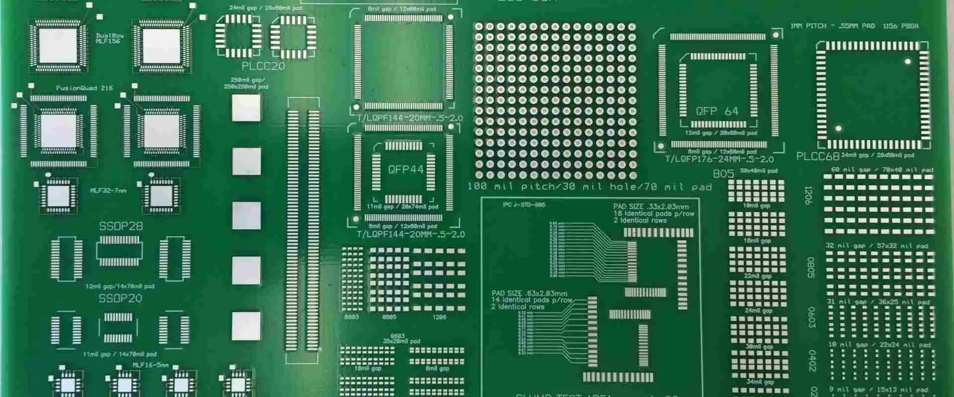
In the sensing as well as control community of several industries, including industrial, agricultural, construction, transport, and business, SMD micro switches have evolved into crucial components. Therefore, industrial machinery, agricultural or construction equipment, and control systems are employed worldwide with billions of micro switches.

These switches are compact, easy-to-use devices with two NC and NO contacts coupled by a switching snap-action mechanism. These switches can operate in a variety of demanding situations securely, dependably, and correctly.

What Does a SMD Switch Offer?

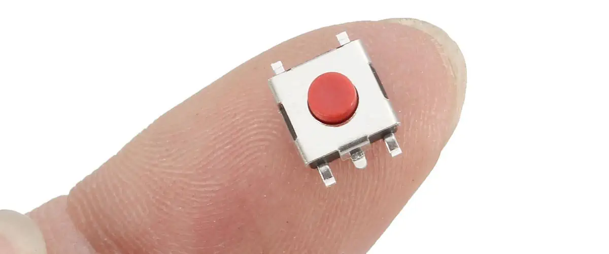
The SMD Micro switch can be described as a switch which can operate quickly and with a very small quantity of force (pressure/push). They are easy to use, quick, and dependable. A small snap-action switch is another name for a SMD micro switch.

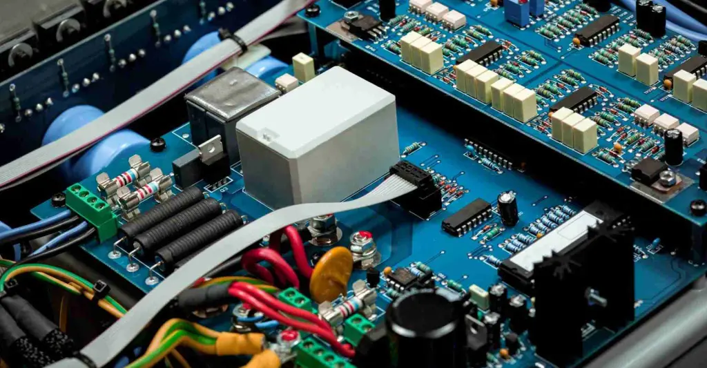
Without the micro switches, modern smart applications for appliances would not be possible. SMT micro switches are utilized in different electronic devices serving different industries, including but not only limited to automotive, medical equipment, aviation, beauty appliances, communications, and home appliances.

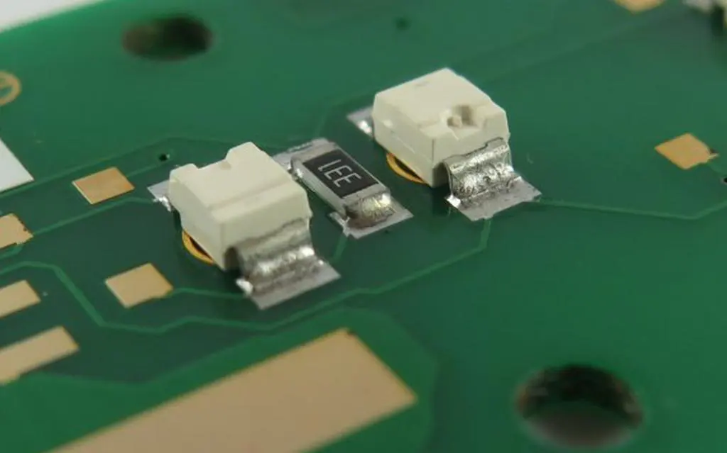
A SMD micro switch, often referred to as a microscopic snap action switch, can be described as a small, extremely sensitive switch which operates with the least amount of physical force. This particular type of these momentary contact switches are frequently employed as a good sensor in the industrial, medical, and automotive equipment.

These switches are widely utilized in home appliances featuring small buttons and switch panels. These switches often cost little money and last for a very long time. Due to their being sensitive and dependable, these switches could be utilized as a safety equipment.

How Does the SMD Micro Switch Work?

SMD Micro Switchs

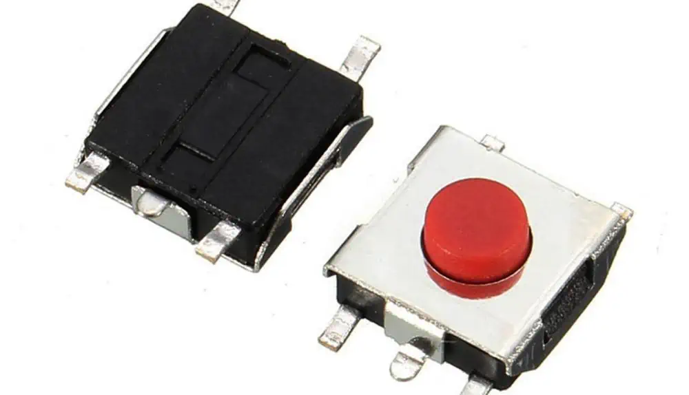
An actuator on a SMD micro switch lifts up a lever whenever it is depressed, positioning the contacts as needed. When pressed, the micro switches frequently emit a type of clicking sound that alerts the user to the actuation.

Also, micro switches frequently come with mounting holes to ensure that they are quickly placed and fixed. Due to their simplicity and extended lifespan, they hardly need to be replaced and require almost no maintenance.

Additionally, this tipping-point mechanism is a key component of the SMD micro switch. As a result, this feature helps in generating particular trips, as well as reset points where contacts would change this condition.

What are the Benefits of the SMD Micro Switch?

The electrical switch known as the SMD micro switch makes or breaks any electrical connection with a small amount of physical movement. It is frequently used in different computer keyboards because it can endure the wears and tears of frequent use over time. Computer keyboards are frequently utilized. The following are some benefits of employing a micro switch.

Optimal Performance

The name of the game when it is something pertaining to the SMD micro switch is precise performance. They need extremely little force in order to function because they come very little and small, so there is less room for error. As a result, you won’t have to be concerned about someone using your switch by mistake due to the fact that it’s too simple to use.

The greatest time to use this kind of switch is when you wish to control a specific item, such as doorbell or light bulb. For instance, rather than simply leave a light bulb sitting about where anyone can easily reach it, you might use the SMD micro switch when you only have a light bulb someplace in your house and want nobody else to be able to switch it on.

Rapid Switching Rates Reduces Arcing Damage

In many commercial and industrial contexts, it’s crucial to be able to easily and quickly switch between several circuits. In sectors including computer networking as well as telecom, industrial switches have been frequently used in turning the power off and on, safeguard expensive equipment from any damage, as well as manage any complex data flow.

The commercial switch industry provides the following significant advantages:

For instance, if you want to be sure that your equipment is well protected from any possibility of damaging surges, switching between the two distinct AC power types can be crucial. Additionally, in the industrial automation area, you must have the ability to quickly and continuously turn equipment on and off.

Applications of SMD Micro Switches

FULL PCB MANUFACTURING Quote

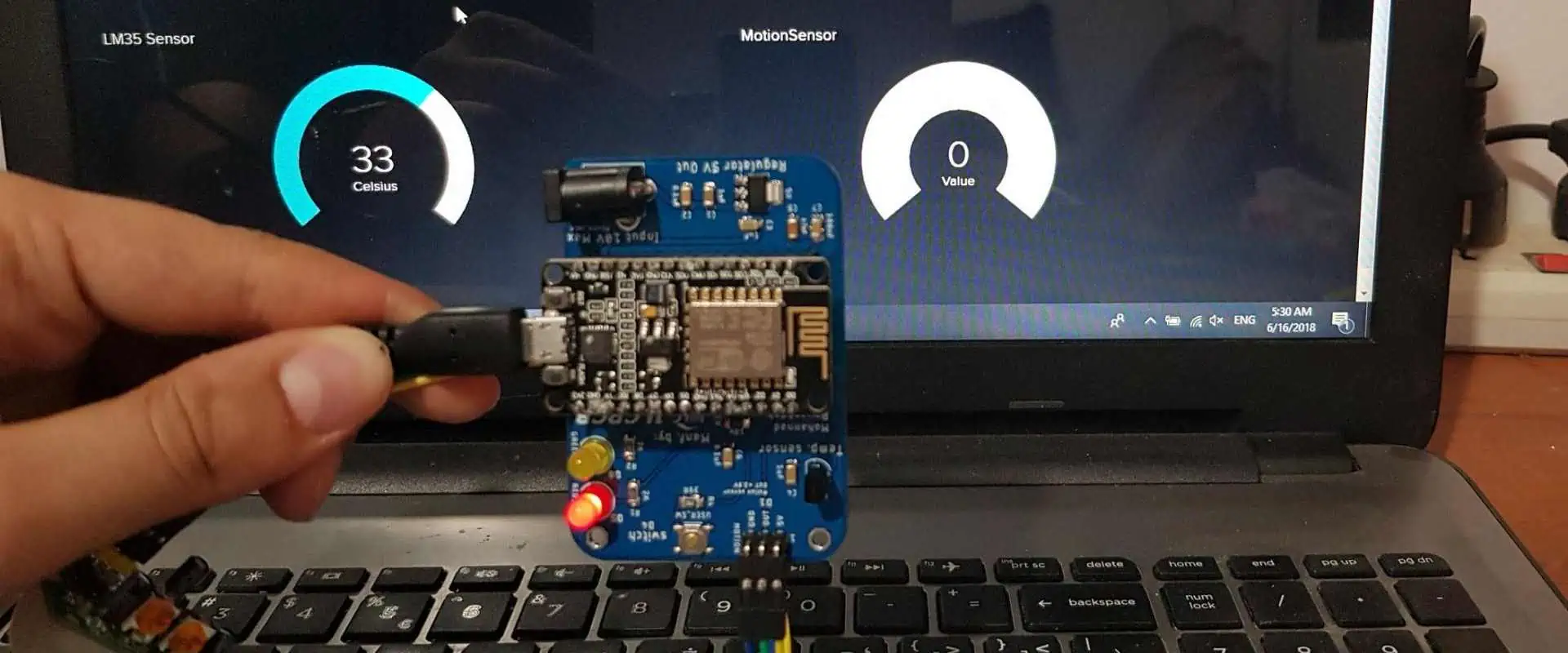
Numerous industrial applications include the usage of the SMD micro switch. The on and off switch, which enables the user to turn anything off or on remotely via an actuator, a sensor, as well as other device, is the most typical application for the SMD micro switch.

Providing the analog input, which may transform the input voltage into an output voltage, which is proportional to its input voltage as well as proportional to any changes in input voltage, is another application.

Electrical appliances like lights, motors, sensors, and relays can all be controlled by micro switches. In robotics, in which they are frequently referred to as actuators since they produce motion rather than turning on and off, micro switches can also be employed. The SMD micro switch mounted to the robot arm is one example. Several motors which move its arm are turned off and on whenever its arm rotates.

These switches are widely used in home appliances having small buttons and switch panels. These switches often cost little money and last for a very long time. Given that they are dependable and sensitive, these switches could be utilized as a safety equipment.

Common SMD Micro switch applications include

  • Alarm as well as call point pushbuttons
  • Turning on surveillance equipment
  • Alerting triggers if there is a dismounted device
  • Control panels for gaining access
  • HVAC applications
  • door locks and elevator  buttons
  • timer controls
  • buttons for washing machine, detection of water level, and door locks
  • AC units
  • Refrigerators – both water and ice dispensers
  • microwave ovens and rice cookers – door buttons and locks

Conclusion

The SMD micro switch plays a crucial role in how a gadget works. Without them, the device would only function as a paperweight because they enable effective communication between the various parts of the apparatus. Since they are compact and contain the essential pressure to help activate them, SMD micro switches are dependable.

These switches could be installed in a variety of objects, including toys, instruments, as well as clothing, but it may be difficult to find them in nearby electronics shops.

How to Calculate SMD Pad Sizes

SMD Pad

Non solder mask defined (NSMD) as well as solder mask defined (SMD) pads are the two main types of the land patterns utilized for the surface mount pads. The solder mask aperture on NSMD pads is larger than that of the pads themselves. In contrast, this solder mask hole on SMD pads is narrower than on copper pads.

What are SMD Pads?

As its name suggests, SMD pads specify the apertures of the solder mask used on BGA pads. The apertures of this solder mask for SMD pads are designed with a narrower opening than that of the pad’s diameter that they are covering. Because of this, any copper pad into which the soldering of the component is done to shrinks in size.

What are Non-SMD Pads?

SMD Pads

As opposed to SMD pads, non SMD pads are distinguished by the solder mask never making physical contact with its copper pad. Rather, this mask is designed to leave a space between the pad’s edge as well as the soldermask.

The solder mask is put on some copper foil to create the SMD pad, while the unmasked copper foil serves as the pad. Copper pads are larger than soldermask openings. The fine pitch component can be used with solder mask specified pads, which are frequently utilized with BGAs. Also, the solder mask usually overlaps on the top of the pcb region between the adjacent pads.

Advantages and Disadvantages of Soldermask Defined Pads

SMD pads have the following benefits:

  • These pads would significantly increase the pad’s strength.
  • It strengthens and increases the dependability of BGA.
  • It’s a wise decision for electronic portal products.

The following are the drawbacks of SMD pads

  • Worse solderability: A high temperature inside its reflow oven will influence the Solder Mask, which would also affect the solder paste’s tin area.
  • Worse location of pads: Because soldermask tolerance is greater than copper tolerance, the size and placement of these pads may be affected.
  • As this copper area grows, its trace area decreases proportionately and also the design of the trace becomes increasingly challenging
  • Its fabrication process seems to be more challenging and demands high precision, significantly raising the cost of manufacturing

Are PCB Footprints More Than the SMD Pad Sizes?

FULL PCB MANUFACTURING Quote

While the size of the SMD pad you select in the PCB footprint plays a crucial role, there are additional elements to consider in the footprint to guarantee the success of the design.

  • Silkscreen displaying part outlines, pin indicators, and the reference designator’s location.
  • Information about the assembly layer to be included in the drawing of the PCB assembly.
  • Opening of a solder mask having a PCB design rule-compliant expansion value

The opening layer of the solder mask and related clearance guidelines are crucial for avoiding DFA mistakes in design as well as subsequent assembly issues. To ensure that your board is error-free, consult the fabrication as well as the assembly team for insight on these issues.

How to Determine SMD Pad Sizes

Determining the pad size for different SMD components can be done in a number of different methods.

The component type as well as mounting method will also affect the precise determination of the pad size. For instance, leadless packages (such as QFNs) as well as leaded packages have different requirements for pad size than BGAs (such as gullwing leads or SOIC). In general, pads provide more space for the solder fillet and are bigger than component leads.  IPC-7351 standard outlines these points in the manner given below.

Standard IPC-7351B

The specifications for the land patterns meant for typical components are provided by the IPC-7351B. This also gives information on calculating pad sizes. Therefore, if you wish to calculate pad sizes manually, you can go ahead.

SMD vs. NSMD Pads: Whatโ€™s the Difference?

SMD-Soldering

The majority of EMS providers advise using NSMD since it gives stricter control of the registration of the copper artwork in contrast to the tolerance process of its solder masking.

Additionally, the definition of the SMD pad might create stress concentration locations that, in the event of excessive fatigue, could lead to solder joint breakage.

To ensure balanced load on solder joints for NSMD, its pad sizes are often lowered by 15% more than the BGA diameter. Additionally, by using this technique, the primary layer’s routing channel may be expanded.

More information to assist you choose between NSMD and SMD for your designs is provided below:

  • While utilizing non SMD pad sizes for BGA 0.4mm pitch PCB design might produce good results in small quantities, there is a good risk that low yields may occur in large quantities.
  • Bear in mind that 0.4mm pitch BGA ball sizes are smaller compared to 0.5mm pitch BGA ball sizes. Further pad reduction may result in BGA pads having insufficient solderable surface. This may result in latent failures inside the field or PCBs rejected during assembly inspection.
  • When employing NSMD pads to serve 0.4- as well as 0.3mm pitch BGA, bridging can occur between pads. Because there is insufficient soldermask webbing in-between the pads, bridging develops.
  • The pad might come off during the reflow or during the field since the pad sizes have become so small and obviously, there isn’t soldermask webbing that can give adhesive strength.
  • Ideally, there should be no trace seen between any adjacent BGA pads. They introduce shorts for external layer pitches of at most 0.4mm.
  • There should only be a single trace in-between the pads on interior layers.

Conclusion

According to applicable standards like the IPC782 standard, the SMD pads for larger components (like sockets, transistors, etc.) must be adequately stretched. For example, SOT23 pads could be extended by about 0.8 to 1 mm. It will really prevent any missing solder caused by the component’s “shadow effect.” Depending on the component’s size, the size of the pad is decided. The best soldering results are achieved when the pad’s width is equal or more than or equal to the component leads’ width.

What Does Assembly Electronics Manufacturing Entail?

smt assembly equipment

Due to their vast range of uses, electronic gadgets and devices are a necessary component of modern living. However, when there is no electronic assembly, they would not be viable. Electronics assembly is a step in the production process for all appliances that improve lives, including air conditioners, smart automobiles, refrigerators, and homes.

What Does Electronics Assembly Mean?

Soldering, gathering, as well as integrating electrical circuits to carry out at least one unique function is the general process of electronics assembly. It is a crucial step in the production of common electronic devices including computers, phones, toys, engines, and remote controls. This assures that the printed circuit board, that is the core of all disassembled electrical devices and gadgets, is functional.

A circuit board is primarily identifiable as an unique green chip covered in copper components and lines. The manufacture of electronic devices and products uses the term “electronic assembly.”

What Do Assembly Electronics Manufacturers Do?

Electrical Engineering For electrical devices in a variety of industries, businesses manufacture as well as test printed wire boards, circuit board assembly, cable harnesses, cable assemblies, and printed wiring board. For a variety of reasons, hiring a 3rd party to produce these assemblies seems to be quite beneficial.

Your duties as an assembler of electronic equipment involve working in factories to put together various computer as well as electronic elements. Additionally, you must adhere to all relevant industry, governmental, and safety norms. Additional requirements for this position include soldering, routing, as well as cutting of the electronic parts.

What are the Benefits of Assembly Electronics Manufacturing?

Smaller businesses with low volume production builds can benefit from the flexibility and fewer human resource concerns provided by assembly electronics manufacturing Companies. Additionally, assembly electronics manufacturing Companies are made to focus on achieving significant manufacturing scale savings by acquiring raw materials, and combining resources, particularly industrial design knowledge.

Additionally, they offer value-added services like subsystem integration, engineering design, functional testing, manufacturability assessments, and troubleshooting services. The consumer benefits from having less need to produce and maintain large product stockpiles. Due to this, the client is better able to react swiftly and effectively to abrupt increases in demand.

Processes Involved in Assembly Electronics Manufacturing

pcb box building assembly services

Through-Hole Assembly Process

Pin-through-hole components are placed into electronic circuits using the Through Hole technique, which involves drilling holes into circuit boards.

The leads, or ends, are then connected to pads present on the opposing side using reflow soldering or wave soldering tools and metal solder that is molten in nature. Additionally, the entire process can be referred to as through-hole assembly.

Early methods of electronics assembly, like point-to-point construction, were replaced by through-hole technology. Every component present on a standard PCB was indeed a thru-hole component from the 2nd computer generation during the 1950s till surface-mount technology gained popularity during late 1980s.

Surface Mount Assembly Process

Electronic circuits built using SMT have their components put directly on the PCB surface with the solder paste.

Surface mount devices are electronic devices created in this manner. Because SMT components can have no leads or smaller leads, they are often smaller than their through-hole counterparts. In SMT technology, the three essential phases are paste, insert, and reflow.

The Mixed Technology

The complexity of electrical items is rising as a result of recent innovations. These sophisticated electrical gadgets require PCB boards that are more intricate, integrated, and compact. It is nearly impossible for circuit board assemblies having just one kind of component to carry out such intricate duties.

Consequently, mixed technology boards having both SMD as well as through-hole components would be needed for this application. These types of boards combine SMT technology and through-hole technology since they contain both SMD and thru-hole components.

However, soldering is indeed a challenging procedure that is frequently impacted by an excessive number of factors. Therefore, improving the order in which SMT and through-hole technology are introduced becomes extremely important.

Process of PCB Assembly – A Step in the Assembly Electronics Manufacturing

FULL PCB MANUFACTURING Quote

An essential step in the fabrication of assembled electronics is the process of PCB assembly. Solder paste onto the circuit board, selecting and arranging the components, soldering, the inspecting, and testing are all steps in this procedure.

For the production of products of the finest quality, all of these procedures must be followed and supervised. Since almost all Circuit board assembly nowadays employs SMT technology, this PCB assembly technique detailed below implies that the components of surface mount are being employed.

Solder paste

Before attaching the components onto the board, the solder paste must be applied to the portions of the circuit board where this solder is needed. These regions are typically called component pads. The solder screen is used to do this.

This solder paste can be described as a mixture of flux and tiny solder grains. This could be put in place using a method that is quite comparable to some methods of printing.

Also, a runner gets driven across this solder screen, which has been mounted directly to the board as well as recorded in the proper location, and squeezes a small quantity of solder paste via the screen’s holes and to the circuit board.

Solder is only deposited on its solder pads since its solder screen was created using the files of the circuit board and has holes where these solder pads are located. To guarantee that the final joints possess the appropriate amount of solder, the quantity of solder which is deposited should be managed.

Pick and place

The board having the additional solder paste has now been sent into pick and place stage. Here, components are picked up from reels as well as other dispensers by a machine that is stocked with component reels, and they are then placed in the right spot on the circuit board.

Soldering

The following assembly stage, known as soldering, begins after the components is now placed to the circuit board. This process involves passing it via a soldering machine.

Even while some boards might be put via a machine for wave soldering, this method is no longer frequently employed for the components of surface mount. Solder paste should not be applied to the board when using wave soldering because the machine for wave soldering provides the solder. Also, the reflow soldering are more frequently employed than wave soldering.

Inspection

The boards are frequently examined once they have undergone the soldering procedure. Boards for surface mount with 100 or more different components cannot be manually inspected. Automatic optical examination is a much more practical alternative. There are machines which can inspect boards as well as find bad joints, missing components, and occasionally the incorrect component.

Test

Before they exit the plant, electronic products must be tested. They could be tested in a variety of ways. The “Test as well as Measurement” part of the website contains more perspectives on test methodologies.

Factors to Consider when Choosing an Assembly Electronics Manufacturing Company

PCB assembly cost breakdown

Longevity and experience in the industry

To sustain a successful business connection, your new or existing company needs to be aware of the extensive background and knowledge of that manufacturer of electrical components. You can count on those established companies to deliver high-caliber work. Additionally, such businesses will take care in creating each board.

Design skills and competencies

Your outsourcing vendor ought to be able to assist you in addition to giving your consumers a top-notch assembly electronics manufacturing company that assists the design procedures.

Also, they should have the expertise to offer recommendations and input on developing any component so that the client can get a variety of viewpoints that might be helpful for the finished project. Consequently, a leading electronics manufacturing firm can assist you in making your goals simpler and more successful.

Product Testing

To verify all quality compliances, the electronics box construction assembly should be carried out. Product testing also is very important to verify that all designs meet high quality requirements. Therefore, a leading electronics manufacturing firm should provide the report for quality assurance in order to prevent any type of production faults.

Environmentally friendly

Also, it would provide you with a much better picture of the company’s environmental worries if the assembly electronics manufacturing companies you choose to work with discloses them.

Large quantities of toxic waste are generated by electronic devices, thus effective trash disposal practices present a favorable impression of your business.

Advancement of technology

Giving your company to an electronics manufacturing service that makes use of all cutting-edge technology is what you would like. It will guarantee that all your products could be produced in an extremely competitive market.

Industry compliance

The assembly electronics manufacturing Companies must be informed of the standards of the industry and follow those standards for their own products. They also should produce box assemblies in accordance with the protocol of quality assurance.

Conclusion

There are various distinct steps in the assembly, production, as well as manufacturing process for electronics. However, to work hand in hand so as to create an integrated process overall is very necessary.

Apa Itu IoT: Understanding What IoT is all About

Apa Itu IoT

The Internet of Things, or IoT, is a collaborative network of interconnected gadgets and technology that makes it possible for gadgets to talk to each other and to the cloud. With the development of low-cost computer chips as well as high-bandwidth telecommunications, the number of devices with internet access has increased dramatically. This implies that commonplace gadgets like vacuum cleaners, vehicles, and machinery can employ sensors to gather information and reply to consumers in a smart way.

Everyday “everything” is integrated with our internet thanks to IoT. Since the 1990s, computer developers have started incorporating sensors and CPUs into commonplace items. However, because these chips were big and occupied up a significant amount of room, initial progress proved difficult. RFID tags are little computer chips that were initially utilized in tracking costly equipment.

Such chips have evolved over time to become smaller, quicker, and smarter as a result of the reduction in size of the computer hardware. Today, it is more cheaper to incorporate processing power into tiny items. An MCU having below 1 MB of the embedded RAM, like the light switch, can, for instance, provide connectivity having Alexa voice functionality.

With the emphasis on saturating our homes, companies, as well as offices with different IoT gadgets, entire industries are grown. Automatic data transmission from and to the internet is possible with the smart objects. The term “Internet of Things” or Apa Itu IoT refers to both the “invisible computing gadgets” and the related technologies. For those new to the work Apa Itu IoT, it is an Indonesian way of asking what IoT is all about.

How Well Does IoT function?

Apa Itu IoT Device

Typical IoT systems function by gathering and exchanging real-time data. There are three parts to the IoT system:

Smart device

We can describe this as items that have received computational capabilities, such as televisions, workout equipment or security cameras. These gadgets gather information from the user input, environment, or usage trends and transmit it from and to IoT apps through the internet.

Applications of Apa Itu IoT

IoT applications are a group of services and programs that combine data from numerous IoT devices to analyze such data as well as make wise decisions, the program utilizes machine learning tech or AI (artificial intelligence). Your IoT device receives this decision and communicates it back; your IoT device therefore reacts intelligently to this input.

Graphical and Interactive User Interface

A graphical and interactive user interface can be used to manage IoT devices including device fleets. Examples of this type are mobile applications, as well as websites which are useful for registering and controlling smart devices.

Examples of Different IoT Devices in Use Today

FULL PCB MANUFACTURING Quote

Let’s examine some current IoT system usage examples:

Connected vehicle

There are numerous ways for connecting automobiles and other vehicles to a internet. It could be done with the dash cam, an infotainment system, as well as a gateway that connects to the car. They gather information from the fuel tank, wheels, brakes, speedometer, odometer, accelerator, and brakes to track both driver efficiency and vehicle health. There are many applications for connected cars:

  • Keep an eye on rental cars to boost economy and cut costs.
  • Assist parents in monitoring their behavior of their child behind the wheel.
  • Anticipate and prevent the need for vehicle maintenance;
  • Automatically notify family and friends in the case of an automobile crash.

Connected Homes

The primary goals of smart home appliances are to increase home networks, efficiency, as well as safety. Smart plugs keep track of electricity use, while smart thermostats improve temperature control. IoT sensors can be used by hydroponic systems to monitor gardens, whereas the IoT smoke detector will be able to identify tobacco smoke.

Security cameras, door locks, as well as water leak detector are examples of a home security system that can identify and stop dangers as well as notify homeowners. Home connected devices are useful in these areas.

  • Automatically switch off inactive devices.
  • The administration and upkeep of different rental properties.
  • Locates misplaced belongings like wallets or keys; automates regular chores like vacuuming and brewing coffee.

Smart Cities

IoT applications for smart cities have improved the efficiency of urban infrastructure and planning maintenance. IoT applications are being used by governments to address issues with infrastructure, environment and healthcare. The IoT applications are useful for  

  • Measuring radiation levels and air quality
  • Use smart lighting system to lower energy costs
  • Determine when vital infrastructureโ€”like roads, bridges, as well as pipelines, needs maintenance.
  • Boost revenue with effective parking administration.

Smart building

IoT technologies are being used in structures like commercial and academic campuses to boost operational efficiency. These IoT devices could be utilized in different smart buildings in order to:

  • Lower costs of maintenance
  • Increase workplace productivity
  • Reduce energy usage

What is Apa Itu IoT for Industry?

Arduino IOT

Smart devices utilized for corporate manufacturing, healthcare, retail, and other industries to improve business efficiency are referred to as industrial IoT denoted as IIoT. Industrial equipment, such as sensors and machinery, gives business owners precise, real-time data, which are useful for improving business processes.

In order to cut expenses and expand income streams, the tools offer insight into the management of the supply chain, logistics, production, and human resources.

Let’s examine current smart industrial solutions from diverse industries:

Manufacturing

Corporate IoT uses wearable technology to increase worker safety and predictive maintenance for decreasing unexpected downtime. IoT applications may anticipate machine problems, minimizing production downtime. Workers are alerted to possible dangers through wearables like wristbands and helmets, in addition to cameras for computer vision.

Car

Robotics and analytics powered by car sensors increase productivity in auto assembly and service. For instance, real-time 3D photographs of interior car components are provided by industrial sensors. While IoT system places orders for new parts automatically, diagnostic as well as troubleshooting tasks may be completed considerably more quickly.

Transportation and Logistics

Management of the supply chain, which includes vendor interactions, inventory management, fleet management, as well as scheduled maintenance, can be facilitated by industrial and commercial IoT devices. Applications from the Industrial Internet of Things are used by shipping corporations to monitor assets and manage fuel usage on the shipping routes. This method works particularly well for tightening refrigerator container temperature controls. Through clever routing as well as rerouting algorithms, the managers of the supply chain are able to make educated forecasts.

Retail

Amazon fosters innovations in automation as well as human-machine teamwork. Robots connected to the internet are used in Amazon facilities to track, locate, sort, as well as move products.

How can Apa Itu IoT make our lives better?

The impact of the Apa Itu IoT on people’s jobs and lives is extensive. IoT makes it possible for machines to perform laborious jobs and lift large objects, improving life quality and productivity.

Connected devices, for instance, can drastically alter your daily routine. Your alarm will start the coffee maker and open the window blinds when you push its snooze button. Additionally, your refrigerator would automatically order the final materials and deliver them to your house. Your smart ovens can even pre-cook some of the ingredients as well as ensure that your lunch is prepared. This would tell you what’s on the menu for the day. Whenever your linked automobile automatically instructs the GPS to halt for fuel, your smartwatch would plan a meeting. There are countless opportunities available in the IoT world!

What Advantages does Apa Itu IoT have for Businesses?

Boost innovation

Businesses have access to cutting-edge analytics through the IoT, which opens up new possibilities. For instance, a company can develop extremely focused campaigns for data collection regarding the behavior of customers.

With ML and AI, turn data to knowledge and action

Future results can be forecast using collected data as well as historical trends. To predict the maintenance incidents, for instance, warranty information could be combined with IoT data. This service has the potential to increase client loyalty as well as proactive client service.

Increased safety

Physical and digital infrastructure may be continuously monitored to improve performance, boost efficiency, and lower safety hazards. For instance, onsite monitor data paired with firmware and hardware version data can be used to schedule the system updates automatically.

Scale differentiated approaches

IoT technology has the potential to boost satisfaction by putting the customer first. For instance, it is possible to swiftly replenish a popular item to prevent shortages.

What do IoT Technologies Entail?

IoT systems employ a variety of technologies, such as edge computing.

Edge Computing

The term “edge computing” describes the technology that allows smart devices to perform tasks rather than simply transmit or receive information to their own IoT platform. The calculation improves the response times, lowers communication latency, as well as boosts computational power somewhere at the IoT network’s edge.

Cloud Computation

IoT device management and remote storage of data are made possible using cloud technology, allowing various devices on a network to access data.

Machine learning

The algorithms and software used in processing data as well as make choices in real time are referred to as machine learning. The machine learning technique is deployable on the edge or in the cloud.

Conclusion

Businesses across a range of industrial sectors require the Internet of Things to exist in the current digital transformation era. Many organizations will eventually be able to successfully evolve as a result of IoT, producing complex products and services using integrated and smart technologies.

The Method, Benefits, and Drawbacks of the ENIG Plating Circuit board

ENIG PCB

The surface finish is necessary to complete a circuit board. PCB surface treatments come in a variety of varieties. The difficulties of varied operational conditions must be endured by PCBs. Consequently, surface finishes must be applied to the printed circuit. One often utilized surface treatments is ENIG plating. More information on this sort of surface treatment is provided in the article.

What Does ENIG Plating PCB Mean?

An ENIG surface finish has gold on top of the nickel layer. ENIG plating offers some oxidation and corrosion resistance. Additionally, the industry uses this surface finish extensively. This is due to the product’s RoHS compliance. Two layers of coating are used in ENIG plating Circuit board. The materials utilized in this kind of plating are gold and nickel.

The nickel acts as a specific barrier between the copper pads and the air. Additionally, it is a substance whereby the maker solders the parts. Gold, meanwhile, provides low level of contact resistance and protects the nickel. The term “immersion gold” also applies to ENIG plating. One advantage of the immersion gold involves its ability to electrolessly bond both nickel and gold to copper.

ENIG plating is covered with a gold layer during gold plating. In addition, this immersion gold layers acts as an oxidation-resistant barrier. Preventing chemical reactions is one of the many advantages of ENIG plating.

Therefore, PCB designers generally like this surface treatment. In ENIG plating, conventional electroless nickel and the gold layer are combined. Additionally, this coating can stick to metal substrates like aluminum. This surface finish is perfect because of the nickel coating. Nickel is also appropriate for the process of lead-free soldering.

ENIG plating circuit board uses a brief immersion to apply gold. Additionally, enig uses the displacement principle. Additionally, this plating applies a thin gold layer by dispersing its surface atoms. Parts that require soldering can have their shelf life extended with ENIG coating. Additionally, it provides outstanding electrical performance.

Process of the ENIG plating Circuit Board

PCB Manufacturing with Immersion Gold-ENIG Surface Finish

Surface Preparation

Before plating, this PCB surface needs to be exceptionally clean. Additionally, there must be no dirt on this surface. Surface preparation is the first step in the gold plating process. This same PCB surface may also be stripped or polished in this process. This procedure uses water as well as any abrasive materials.

Micro etching

In this procedure, the copper plate’s roughness is eliminated. This process aids in strengthening its copper surfaces as well as electroplated layers. Additionally, it raises PCB quality.

Activation of the immersion gold

Use of copper plating parameters is required for this phase. The thickness of the nickel layer can be adjusted. The nickel-plated pads are dipped by the manufacturer in the gold water. This gold can then be removed from the solution. The final step is to clean the surface of the pad to ensure that there is no dirt on it.

Benefits of the ENIG Plating Circuit Board

FULL PCB MANUFACTURING Quote

Employing ENIG plating has a number of benefits, such as:

Good resistance to oxidation

Manufacturers of PCBs with experience favor surface finishes which can withstand oxidation. PCBs with immersion gold plating provide excellent oxidation resistance. Additionally, this sort of circuit board surface treatment includes immersion gold above the electroless nickel plating. The gold coating inhibits oxidation of the nickel. Consequently, ENIG plating guarantees a printed circuit’s resistance to corrosion.

Withstand high temperatures

An important benefit of the ENIG plating is this. The majority of circuit boards utilized in military and medical equipment operate at high temperatures. In these situations, ENIG plating can be described as the best solution for PCB surface finishing. Additionally, ENIG is suggested since it can endure high temperatures. Excellent thermal diffusion capabilities can be found in an ENIG coating. In addition, this ENIG plating can resist very high temperatures.

It is lead free

Both humans as well as their environment can be poisoned by lead. Health problems may result from lead exposure at high amounts. ENIG plating is lead-free. Additionally, this implies that harmful compounds really aren’t exposed to PCB makers. As a result, ENIG plating is frequently utilized in electronics.

For use on untreated surfaces

It is crucial to protect these untreated surfaces from oxidation. Based on the surface finish type utilized, this exercise may be difficult. For untreated surfaces such as membrane switches as well as contact points, ENIG plating is appropriate. Additionally, immersion gold provides superb surface planarity. This makes it appropriate in comparison to other surface treatments.

RoHS conformity

The RoHS directive forbids the use of around ten of the most harmful materials in the manufacture of electronic equipment. ENIG plating usually meet all the ROHS requirements. Here is one good reason why circuit board designers usually love this type of surface finish.

What are the Cons of ENIG Plating?

ENEPIG and ENIG
ENEPIG and ENIG

Black pad

Black pad is an undesirable structure that appears during ENIG plating. Additionally, this is caused by a sulfur-based chemical leaking from this solder mask. Electrical isolation may result from black pad development. Black pads are unable to transmit the electrical charge, which explains why. Black pads may also result in surface cracks on your PCB. As a result, good solderability and evenness may be compromised.

Poorly soldered joints

Weak solder junctions may result from inadequate wetting. Additionally, the circuit board may have a kind of weak connection as a result of this. Electrical continuity loss may be the result of inadequate wetting.

Really pricey

ENIG plating is very expensive. Compared to other PCB surface coatings, this is much more expensive. Additionally, it costs more than OSP and HASL. Gold and other expensive materials are used in ENIG plating. This type of surface finish cannot be reworked, either. As a result, ENIG plating is quite expensive.

Loss of signal

When used for a long time, ENIG plating may undergo signal degradation. As a result, this may have an impact on your PCB’s general performance.

Conclusion

The circuit boards are essential to how electronic gadgets operate. For the PCB plating, a variety of surface treatments are offered. An excellent option for PCB assembly is ENIG plating. Additionally, this kind of surface treatment is perfect for usage in areas where corrosion resistance is necessary.

How IoT Based Projects are Saving Lives and Properties in Our World Today

IoT Based Projects

A lot of things have been said about the Internet of Things. As the world keeps evolving, technology keeps advancing. All of these things have an impact on our daily lives from how we do our shopping to the way we travel. The Internet of Things, popularly known as (IoT) refers to the connection of any device to the Internet and some connected devices.

Also, the IoT is a network of connected people and things which receive and share data about things happening around them. Therefore, one can simply say the Internet of Things (IoT) refers to physical devices that are linked to the internet, all receiving and sending data. IoT is merging the physical and digital worlds.

A physical object can become an IoT device if connected to the internet. An example of an IoT device is a light bulb you can easily switch on with the use of a smartphone app. The motion sensor in an office connected to streetlight is a good example of an IoT device. A smartwatch or other wearable device is an example of an IoT device.

Top IoT Based Projects

Arduino IOT

There are several IoT projects. These projects have made our lives easier one way or the other. Below are some IoT based projects around you.

Smart street lighting monitoring system

Most times, streetlights are usually left on during the day. This is a major challenge in the street lighting system. Therefore, IoT profers a solution to this major challenge by enabling the monitoring of street lighting system with the introduction of a smart street light. Also, this system will help to detect faulty light, monitor power consumption.

The smart street light has LDR sensors. These sensors monitor peopleโ€™s or vehicleโ€™s movement on the street. Therefore, if they detect movements, they make a signal to the microcontroller to switch on the street light. Also, this street light regulates the consumption of power and as well detects any fault. The IoT monitoring system will fix any fault detected by the street light.

Smart money transfer

The smart money transfer is another example of IoT based projects. In todayโ€™s world, we are gradually heading towards full digitization. With smart money transfer, it is easy to carry out transactions on your mobile phone using Apps like Paypal, Apple pay, and Google Pay.

Smart money transfer offers a reliable and comfortable platform for payment transactions. Also, this system ensures authenticity in order to ensure safety. Furthermore, smart money transfer helps in minimizing the problems that occur during mobile money transfers. It offers a reliable and comfortable platform for any money transactions.

Car parking management system

Car parking is one of the problems vehicle owners face, especially in urban areas. Efficient car parking management system is crucial in urban areas. This helps in solving parking problem. IoT has helped in achieving car parking management system. Also, an IoT based car parking management system helps in utilizing parking space.

It integrates a WiFi modem, IR sensors, an AVR microcontroller, and DC motors. The DC motors monitor gate opener motors and IR sensors detect parking slot occupancy. Also, the car parking management system checks the number of parking slots that are available and then updates information on the cloud server. Furthermore, this system enables car owners to view any free space online. This helps you know where you can park your car.

Health monitoring system

The health monitoring system is another popular IoT based project. Sometimes, people forget to go for their regular checkups, due to the several activities they might be involved in. The health monitoring system helps patients to keep record of all vital signs of the body. Also, this system helps in keeping track of a patientโ€™s regular check-up. It then sends the data to the doctor. If the vital signs are unusual, this system alerts the health care provider.

Air and noise pollution monitoring system

In urban areas, there is an increasing level of air pollution and environmental noise. Therefore, there is an immediate need to control these. With an IoT powered noise and air pollution monitoring system, the level of noise and air pollution can be completely monitored. Also, the data provided by this system can be used in solving further problems.

Furthermore, the system comprises air sensors that detect any harmful compounds and gases in the air and monitors the levels of sounds. The sensors communicate with the microcontroller that transfers this data. Authorities can make use of this data to adopt measures for pollution control.

Smart home security

At one point in our life, we have been a victim of theft. Theft could happen due to a break-in or not paying attention to valuable items. It could be very frustrating to know that your property has been stolen. However, there is a solution to this problem. The smart security system can notify you when someone moves your things without you knowing.

Also, this system prevents thieves from carting away your valuable items. The smart home security system is usually installed in homes to kick against any form of theft. This system makes light and sound alerts whenever an intruder picks your things. It will as well send a notification to your Gmail to inform you someone tried to pick your item. The smart home security system is a good IoT based project.

Smart agriculture system

This is one of the best IoT based projects. Smart agriculture system simply focuses on the development of an agricultural system that is capable of performing and as well regulating farming tasks. For example, a farmer can schedule this system to spray pesticides or fertilizers on the crops.

Also, the smart agricultural system can make use of a moisture sensing system to monitor soil moisture. With this, farmers can easily detect dry soil and as well handle some farming tasks. Furthermore, this system enables cultivators and farmers to focus more on manual-intensive projects. One of the benefits of this system is that it increases productivity. This system offer more benefits like real-time update, accuracy, ease of use, and timely monitoring.

Smart traffic management system

FULL PCB MANUFACTURING Quote

The number of vehicles on the road keeps increasing as population increases. Therefore, traffic congestion is now a problem due to the rising number of vehicles that ply a road everyday. The smart traffic management system as an IoT based project has helped to manage traffic effectively and as well provide clear roads for emergency vehicles.

Also, emergency vehicles can easily connect to this system to look for free pathways. The smart traffic control system gives a green light for any emergency vehicle. Furthermore, this traffic management system can monitor the activities of traffic violators. This system provides safety from any road accidents and real-time traffic management.

Smart energy grid

This is another wonder of IoT. In our world today, energy grids are not well optimized. Most times, when a region experiences a fall in electricity grid, there is blackout in the whole area. Therefore, this could hinder peopleโ€™s daily activities. The smart electricity grid provides solution to this problem.  It integrates the ATmega family controller to regulate and control the system activities.

Also, it makes use of WiFi technology to interact over the internet. The main task of the smart grid system is to enhance the reconnection of the transmission line. Therefore, the system moves to another energy gridโ€™s transmission line in case there is a faulty energy grid. This system monitors the consumption of energy and detects any electricity theft.

Smart waste management system

Cities are keeping up with the IoT projects. They are now integrating this projects in most of their systems. The old practice of waste disposal is now being abandoned and smarter cities are now integrating a smart waste management system. This system sends an alert to waste management team whenever the dustbin is full.

Also, this system separates waste in wet or dry garbage. It helps waste management workers to save energy and time spent on segregating waste in wet or dry garbage. Smart waste management system can help to prevent garbage from overflowing since this system sends alert when the garbage is about to get filled.

Home automation system

Automating homes via the internet is one of the greatest IoT based projects. The home automation system permits the functioning of household devices through the internet. With this IoT project, home owners can connect all their household appliances over the IoT. Also, they can control this device from their smartphone wherever they are.

The home automation system integrates an LCD screen for showcasing system status, an AVR family microcontroller, and a WiFi connection. Also, the microcontroller processes the user commands it receives and displays the system status. The home automation system is becoming popular in some homes in developed countries. With this system, you can easily know what is happening in your home and you can take charge at anytime from anywhere.

Weather Reporting System

The weather reporting system is an IoT based project that forecasts weather around your locations. There are times the weather suddenly changes. The weather is unpredictable due to the climate. It is good to know what the weather will be like in the next few hours, this helps you prepare for what is coming.

The weather reporting system minimizes the need to depend on agencies that specialize in weather forecasting. Also, this system embeds rain, humidity, and temperature sensors that can keep track of the weather and offer real-time statistical reports.

Flood Detection System

The flood detection system is an important IoT based project. Many countries experience natural disasters such as flood. Flood usually cause a lot of damage to properties and lives. One of the best ways to prevent the loss of lives and properties caused by flood is the integration of the flood detections system.

This system helps to forecast flood. The IoT based project detects different environmental elements like water level, humidity, and temperature to forecast possible losses. Whenever a possible loss is forecast, it sends an alert. ย 

What are the Benefits of IoT?

IoT Monitoring

The Internet of Things (IoT) offers a lot of benefits.

Ease of access

With IoT, you can get necessary information about a task wherever you are in the world. A smart device and connection to the internet is what you need. You can easily buy tickets and check your location on Google Maps.

Data monitoring

One of the most important benefits of IoT is data monitoring. For instance, smart street lights can monitor the consumption of power and as well detect any movement on the street. Also, with IoT, you can easily get the additional data.

Automation and control

Internet of Things provides different levels of automation, making it easier for you to do more tasks. Automation helps in achieving uniformity in tasks, regulating daily chores, and improving quality of service. IoT devices are internet-connected devices that offer more enhanced and timely production while maintaining transparency across the whole process with higher quality.

Money saving

Another important benefit of IoT is that it helps you save money. The cost of monitoring devices is much more than the cost of purchasing these IoT devices. For instance, the integration of the smart energy grid system and smart waste management system is a way to save cost. IoT helps you connect your devices with other devices. This helps in saving money and energy.

Time management

One of the benefits of IoT is time management. With IoT, you can do everything you want to do from the palm of your hands. You can make an online purchase, switch on a bulb, and also know when an intruder breaks into your home. Also, healthcare providers can keep track of their patientโ€™s check-ups. IoT makes all this possible.

Conclusion

IoT based projects make life easier. Also, these projects save lives and properties in cases of flood detection, weather forecast, anti-theft, and more. There is a vibrant future for IoT due to the increasing demand for more accessibility and advancement. We have discussed a wide variety of IoT based projects and their impacts in human lives and the environment in this article.

What are the Similarities and Differences of the Raspberry Pi Pico Variants?

Raspberry Pi Pico

Raspberry Pi Pico is a microcontroller development board produced by Raspberry pi foundation. This low-cost and versatile board was constructed around the RP2040 chip. The Raspberry foundation designed the RP2040 chip in-house.  

In January 2021, the RP2040 chip was released. Since then, this development board has gained popularity among the DIY community. More than a year after the first board was released, a few variants of the Pico board was released by the Raspberry Pi foundation. The few variants include Pico WH, Pico W and Pico H. We will be discussing all of these variants, their similarities, and their differences.

Raspberry Pi Pico-Cortex Development Board

This is a new low-cost microcontroller development board produced by Raspberry Pi Foundation. It is sold for $4. The silicon RP2040 SoC powers the Raspberry Pico. The RP2040 SoC comes with an Arm Cortex M0+ processor that runs at about 133 MHz. Also, its SRAM is 264K and onboard storage is 2MB. The Raspberry Pi Pico is an ideal choice for any DIY project.

Unlike other boards earlier developed by the Raspberry Pi foundation, the Raspberry Pi Pico isnโ€™t an SBC that can manage a full OS. ย It can be programmed in C programming or MicroPython languages since it is a microcontroller development board.

The RP2040 offers unparalleled reliability and flexibility to professional s. It features deterministic bus fabric, a large on-chip memory, rich peripheral set, symmetric dual-core processor complex, and deterministic bus fabric. Also, this development board is a great option for hobbyist and beginners due to its UF2 bootloader in ROM and a detailed documentation.

Microcontrollers are very small computers, however, they donโ€™t have large volume storage. Also, they have no peripheral devices that can be plugged in like normal computers.  The Raspberry Pi Pico comes with GPIO pins, which is similar to a Raspberry Pi computer. This means you can use this microcontroller development board to regulate and as well receive input from various electronic devices.

Raspberry Pis were single-board computers that could run an operating system before the advent of Raspberry Pi Pico. Despite, the low cost of Pico, it is a capable device. Pico has a pin header with 40 connections which enables you to directly analyze programs from another computer. ย The Pico ushers users into a new era of Raspberry Pi.

Raspberry Pi Pico W and WH

Raspberry Pi Pico board

In as much as the Raspberry Pi Pico offers a wide range of power features, it has got its own drawbacks. The main disadvantage of this development board is that it lacks wireless connectivity unlike its competitors ESP8266 or ESP32. However, the Raspberry Foundation decided to solve this problem by providing a solution to this problem in the new Pico WH and Pico H. These development boards have wireless connectivity. Therefore, this gives it a better advantage over Raspberry Pi Pico.

The newly developed Pico W features an Infineon CYW43439 chip. This chip is designed to offer to support to Bluetooth LE 5.2. and 2.4 GHz WiFi 4. Although the Chip supports Bluetooth 5.2, it is not functional at this time. In the future, the Raspberry Pi foundation may enable it through some firmware updates.

Asides the recent addition of the Wi-Fi module and antenna, the Raspberry Pi Pico W and WH has similar design with the Pico. Furthermore, the user CYW43439 now connects to the LED, however, the wireless chip can still be controlled from the RP2040 SDK.  Also, it is pin-to-pin compatible with the Raspberry Pi Pico. Therefore, add-ons or carrier boards already existing should be able to work without any modifications.

The Pico W has a buck converter that can be changed to meet the new power requirements. Rather than using the RT6150B as its power regulator, the new Pico integrates the RT6154A by Richtek . Also, the debug port moved close to the SoC to create space for the Wi-Fi antenna.

Pico W has similar size with Pico. This board features many GPIO and supports MicroPython. Also, this board has a wireless interface of 2.4GHz.

Raspberry Pi Pico H

Raspberry Pi 3B
Raspberry Pi 3B

This microcontroller development board shares similar properties with the original Raspberry Pi Pico. These two boards have no differences in terms of their functionality. However, there is a slight difference. Raspberry Pi Pico H doesnโ€™t have the old gold-plated castellated holes in Raspberry Pi Pico. Also, the header pins in Raspberry are pre-soldered.

Also, another difference in these boards is the new debug connector. The Raspberry Pico features 2.54mm standard header pi for debug. On the other hand, the new Pico H comes with a 3-pin SM03B-SRSS-TB connector. This connector is ideal for 2-wire serial debug interfaces or UART. Asides these differences, the Pico H and original Pico has everything else in common. Even the physical dimensions and pinout are the same for both boards.

Specifications and Usage of Raspberry Pico

Pico has impressive specifications. These include:

  • A dual-core processor that operates fast
  • 16 PMW channels
  • Excellent eight programmable I/O
  • Onboard flash memory of 2MB
  • 26 I/O pins which comprises 3 analog inputs
  • Dormant and low-power sleep modes
  • SRAM of 264Kb
  • Clock and timer on-chip
  • USB 1.1 Host and Device support
  • Temperature sensor
  • Drag and drop programming that makes  use of mass storage
  • Castellated modules that enable direct soldering to carrier boards

Although Pico doesnโ€™t feature an onboard Bluetooth and Wi-Fi since these consume much power. However, these features arenโ€™t really necessary. Users can maximize the features of this device, especially professionals. However, Pico is ideal for beginners. Also, beginners can program Pico in MicroPython or CircuitPython.

More Facts about the Raspberry Pi Pico

FULL PCB MANUFACTURING Quote

The Raspberry Pi Pico is ideal for DIY projects. This microcontroller development board is very versatile. In terms of the capabilities of programmable Input/Output (PIO), Pico bridges the gap between hardware and software.

Raspberry Pico has proved itself to be an impressive tool over time. Although it is new, it has got more features and benefits than other Raspberry Pis. The serial wire debug (SWD) header in Pico enables debugging, which helps you track down issues in programs.

Pi Pico features power pins which either power the peripherals and sensors from the pico or power the Pico from the power source.

Best Projects of Raspberry Pi Pico

LCD display interface

With Pico, you can make use MicroPython programming for interfacing an LCD display. This practical upgrade is a great addition to your device since you can make use of LCD displays for several projects.

LoRaWAN

Pico has no native wireless capability. It integrates LoRaWAN. This helps to keep the package low-powered and also interface with real-world sensors. LoRa is a wide-area networking ideal for Internet of Things. Therefore, it can connect low-power devices over impossible distances.

Flashing LED

Pico works differently from Arduino. Flashing LED may not be exciting for some users. However, these projects are easy and quick to run. Also, these small projects helps in setting up and integrating  MicroPython on the Pico.

Color Mandlebrot set

You can easily locate some simple guides on how to link TFT display to a Pico. The Raspberry Pi Pico is much more interesting as it has several new thing to learn about mathematical programming, TFT graphics, and analog input control.

USB foot pedal

This project is useful for hands-free pause when integrating software. The USB foot pedal in Raspberry Pi is ideal for your computer needs. Also, this project is great to pick for several levels of Raspberry Pi users.

SMARS Robot

The I/O  and processing capabilities of Pico makes it easy to build SMARS Robot. The popular modular SMARS robot series is a great project in Pico.

Gaming

This is one of the best projects the Raspberry Pi Pico can handle. The result you get from this project offers you a great method to learn how to transfer designs from various platforms like Arduino.

Music Box

Pico users will love to handle this project. Who doesnโ€™t love to play some nice music. The MP3 is a creative microcontroller application.

What is the Difference Between Arduino and Raspberry Pi Pico?

Raspberry Pi 4
Raspberry Pi 4

The Raspberry Pico and Arduino Uno have been compared together several times since the release of Pico in early 2021. This type of comparison will go on for log since there are many factors to consider in this comparison. Both Arduino Uno and Pico are great microcontrollers, but there are some differences.

There are some differences between these two microcontrollers in terms of memory, power consumption, CPUs, programming languages, pins & I/Os and ease of use. When it comes to price and size, the Arduino Uno isnโ€™t as great as the new Raspberry Pi Pico. However, the specifications of Arduino is a bit similar to that of Raspberry Pi Pico.

For instance, it is easy to program in Arduino since its IDE (integrated development environment) is user-friendly. Arduino devices integrate a variation of C++. Pico integrates a 40-pin DIP style board. This is an added advantage for Pico users. This means Pico has rows of pins with rectangular housing directly soldered on it.

One advantage of this feature is that you can attach Pico to various project pieces. Also, it can be combined with a breadboard. The processor of Raspberry Pi Pico is stronger than Arduino. This means the Pico consumes more power than Arduino. Pico has a better processing power than Arduino , which makes Pico a beast.

Furthermore, the coding language integrated by Raspberry Pi Pico is MicroPython. This language is very easy to pick up. The C and C++ programming language isnโ€™t recommended for beginners. This is because Pico doesnโ€™t have a beginner friendly IDE.

Also, the programmable Input/Output pins are capable of simulating communication protocols and peripherals. You wonโ€™t find this feature in Arduino Uno. ย 

Frequently Asked Questions

Raspberry pi into a Router

Can I Connect a Raspberry Pi Pico to the internet?

Raspberry Pi co W has an Infineon CYW43439 2.4GHz Wi-Fi chip. With this feature users can get exceptional Wi-Fi reception without lots of wires.

Can Raspberry Pi Pico function as a computer?

Raspberry Pi  can copy several devices and the Pico isnโ€™t left out. Eric Badger reveals the ability of Pico to copy a 6502 computer and shows a comparison of the Pico running close to an Apple II computer.

What is the major difference between Raspberry Pi and Pico?

These two boards have no differences in terms of their functionality. However, there is a slight difference. Raspberry Pi Pico H doesnโ€™t have the old gold-plated castellated holes in Raspberry Pi Pico. Also, the header pins in Raspberry are pre-soldered.

How long can Picoโ€™s battery last?

Pico uses a LiPO battery specifically designed for the UPS Pico. The capacity of this battery is more than 3000 mAh. Therefore, this allows users to use the Raspberry Pi Pico for about 8 hours with no power supply connected.

Which is a better option, Arduino Uno or Raspberry Pi Pico?

Arduino Uno and Raspberry Pico both have their advantages and disadvantages. Although Pico is newer than Arduino, these microcontrollers both feature different specifications and this makes them unique. However, the Raspberry Pi Pico is a stronger microcontroller in terms of its processor, PIO pins, and memory. This microcontroller features more pins. Also, its DIP design is very impressive. However, the choice of which microcontrollers you opt for depends on your preference. Another aspect the Pico is a better option is in terms of its PIO pins. The programmable I/O pins can help in combining basic assembly programs.

Conclusion

The Raspberry Pi Pico comes with GPIO pins, which is similar to a Raspberry Pi computer. This means you can use this microcontroller development board to regulate and as well receive input from various electronic devices. Despite the low cost of Pico, it is a capable device. Pico has a pin header with 40 connections which enables you to directly analyze programs from another computer.  

Raspberry Pis were single-board computers that could run an operating system before the advent of Raspberry Pi Pico. Despite the low cost of Pico, it is a capable device.

Applications and Types of Portable Devices PCB

portable devices pcb

Our lives are shaped by portable electronics. Electronics play a significant role in daily life, from mobile phones to different GPS systems in cars. We want them to function as intended under all circumstances, maintain a respectable battery life, as well as operate pretty swiftly, and they accomplish this thanks to PCBs that make up the structural framework of our portable devices.

For any portable electronics application, purchasing the appropriate circuit boards is crucial to producing functional, durable products that customers will adore for many years. Discover more regarding the various PCB-based electronics and the best designs to buy.

What are Portable Electronics?

PCBs are used in the electronics we use each day. Consider your computer, tablet, smartphone, and more. They are all made to fit a lot of usefulness into a little amount of space. All of this is made possible by the PCB, which keeps everything small and light. But portable devices go beyond simply your phone. Think of your morning alarm clock as well as radio or your Bluetooth speaker that you bring to just about every party. Note that they are all powered by PCBs.

Every piece of portable, electrically powered device is referred to as portable electronic devices. These are usually consumer electronics with communication, data processing, as well as utility capabilities. This ranges from portable, lightweight electronics like smartphones, tablets, and e-readers to tiny gadgets like MP3 players as well as electronic toys.

What are Portable Devices PCB?

portable pcb

Considerations for production and design that must meet many requirements are particular to portable electronic devices.

Its internal circuitry needs to be extremely reliable for such application and able to withstand challenging conditions. Large temperature fluctuations, humid and moist environments, electromagnetic interference, physical shocks, and radio frequency interference are all possible for the device.

The electronics must also fit within the constrained space of the product. Phones, fitness trackers, smartwatches, inventory trackers, as well as spectacles for dental operations are just a few examples of the portable electronics that are getting thinner, smaller, and bendable. These sizes must be supported by the type of circuit employed, yet it must also be portable and comfortable to use.

Customers possess three options when choosing the best PCB technology to use: rigid circuit boards, rigid-flex circuits, or flex circuits. Rigid-flex circuits continue to be the preferred PCB for portable devices, despite the fact that rigid boards are ideal for a variety of applications.

Applications of Portable Devices PCB

Innovation in portable electronics sector depends on PCBs. Before HDI technology was developed, electronics, particularly computers, could fill entire rooms. Nowadays, HDI boards are used even by your smartwatches. Laptops, Cellphones, tablets, wearable technology, digital cameras, as well as GPS units all use HDI PCBs. They are now included in IoT products like smart thermostats, the smart refrigerators, and more as technology develops.

Household Applications

The portable devices PCBs are widely useful in household appliances like  clocks, hand drills, cordless cutters, cordless vacuum cleaner, electric salt handheld mixer grinder, paper mills, torches, and rechargeable flashlights are frequently made using PCB.

These are a part of everyday items like kitchen appliances. Portable gadgets are very practical for use, very safe from electric shocks, unaffected by utility power outages, etc.

Multimedia Electronic Devices

These cover devices like iPods, satellite phones, laptops, tablets, and many others. These tools give us flexibility and freedom in our work, communication, and entertainment. You can utilize your smartphone, for instance, when you are standing, sitting, or even lying down. In actuality, we can do the majority of our tasks and personal needs using these multimedia gadgets today.

Personal grooming

The tools we employ for personal grooming include wristwatches, electric shavers, electronic toothbrushes, and hair trimmers.

Common Types of PCBs for Portable Devices

FULL PCB MANUFACTURING Quote

There are numerous PCB possibilities, but three in particular are excellent for portable electronics. The rigid-flex PCBs, HDI PCBs, as well as flexible PCBs. Rigid-flex PCBs combine the advantages of rigid-board with flexible technologies.

Flexible PCBs

For customers wishing to develop electronics which will have weight and space restrictions, flexible PCBs offer adaptable solutions. The operating parts must all fit and work together smoothly without creating friction or tangled wiring and connections.

This problem is overcome by flexible circuits by having less connections and components. Instead, the flex polyimide substrate or FR-4 materials have copper traces that are etched onto them. By using this method, the circuit boards can flex as well as bend around functional components.

The client gets a highly functioning gadget that will work for the application without taking up extra space in the design of the device.

Rigid-flex PCBs

Flexible and rigid-board technologies are combined in rigid-flex PCBs to provide several advantages. When it comes to final installation or manufacturing, they support versatile applications.

Rigid-flex PCBs include flexible layers layered between the rigid layers so as to boost their longevity, whereas flexible boards by themselves frequently are unable to withstand the daily wear as well as tear of the challenging applications used in portable electronics.

They are perfect for various industry-specific scenarios since they may be produced utilizing a number of materials tailored to your particular applications. For the optimal shape for you, rigid-flex Circuit boards must be created in the 3D environment.

Because of its flexible form, it’s a fantastic choice if you wish to conserve space while boosting endurance. Rigid-flex PCBs are thus ideal for compact, portable devices that need more room without compromising on performance.

HDI PCBs

HDI PCBs serve as an alternative to rigid-flex PCBs for portable electronics. HDI PCBs serve as an alternative to rigid-flex PCBs for portable electronics. High density connection boards, sometimes known as HDI, are a vital component of electronics sector.

In contrast to other circuit boards, they have a greater circuitry density for every unit as well as more functionality inside a small space. They can have a number of features, ranging from but not restricted to:

  • Buried vias and through vias
  • Coreless construction having layer pairs
  • A minimum of two layers when working with through vias

The use of the HDI PCB has various advantages. It begins with its lighter weight and smaller dimensions. It is increasingly likely that HDI boards will be present in our electronics as they continue to get smaller. These boards offer increased electrical performance due to a closer spacing between components, which allows them to fit so much functionality in a compact area. Additionally, HDI PCBs remain inexpensive. Due to their compact size, they require fewer raw materials and frequently produce more quickly because the process of manufacturing doesn’t include as much layers or material.

Why Rigid Flex PCBs are Used for Portable Devices

Rigid Flex PCB Assembly

When utilized for portable electronics, rigid-flex boards give the best. The rigid circuit part offers strength and stability towards other parts of that product which need increased durability as well as shock absorption, while the flexible area performs well for items that need it to flex in specific spots. The following elements are some of primary benefits.

Less Packaging

The requirement for the wired connections is greatly diminished and, in some circumstances, eliminated by integrating rigid boards and flexible circuits into a single integrated unit.

Possible Cost Savings

Customers may discover possible cost advantages when using the rigid-flex PCB for their applications because of the reduced material utilization and simpler assembly.

Because only the materials required for final assembly will be charged to customers, the rigid-flex PCB can be packaged in lighter and smaller forms.

Greater capacity

Compared to conventional rigid PCBs with the wired interconnects, rigid-flex PCBs’ flexible PCB sections offer a wider capabilities. This flexible board may easily handle all transmission loads when the design of the product calls for high-speed signals as well as regulated impedance.

Factors to Consider When Designing Portable Devices Design PCB

Via Types

Interconnections between components and layers are made possible through vias. Vias come in a variety of forms, including through, blind, buried, and micro (multilayer, single-layer, or stacked). The appropriate designs reduce the various through kinds. It’s crucial to have a thorough conversation with the PCB provider you’ve chosen to make sure that they can accommodate the through types you want to employ. Additionally, you will have to confirm the carrying capacity of current of the various via types.

Rules for design

These rules will deal with design-specific guidelines, such as component placement, layer allocation, crosstalk budgets, length matching and analysis of flight time, and other issues. Additionally, this will cover DFM guidelines, which guarantee that the final design can be produced; for example, are their via aspect ratios accurate?

Signal reliability

The signal integrity is one element of good PCB design that is most frequently taken into account. An engineer typically takes into account factors like signal fall and rise timings, track lengths, characteristic impedances, drive strength, as well as the drivers’ slew rates.

Conclusion

For portable devices pcb, purchasing the appropriate circuit boards is crucial to producing functional, durable products that customers will adore for many years.

What Does Altium Single Layer Mode Entail?

Altium vs Cadence

Additionally, Altium Designer supports adjusting each object’s transparency separately and for every layer which can be applied to a board design. You now have more control over how things are displayed within the space of your design. Transparency-level parameters can be customized, experimented with, and fine-tuned to meet your needs using the Visibility dialog of the object.

What is Altium Single Layer Mode?

Copper electrical, protective masking, insulation, text, as well as layers for the graphic overlay are some of the layers that make up a PCB.

Along the design space’s bottom edge are tabs for each layer that is usually set visible for the panel for View Configuration. They let you to change the layer that is currently displayed and provide a visual cue for which layer is the highlighted or current layer. Utilize the arrows in going through all the tabs if there are extra layer tabs compared to the number you can show at once.

Altium Single layer Mode Explained

What Does 2D Single-Layer Display Mode Mean?

This Single-Layer mode functions are incorporated with a Board Insight and may be set up on the Preferences dialog’s PCB Editor – Display page of the Board Insight. While all other layers’ contents are either hidden or dimmed in Single Layer mode, the information of the present layer are displayed.

Single-Layer mode features monochrome and grayscale display modes in addition to hiding all the objects present on the other layers just to show the contents present in the present layer.

You can maintain the information of the spatial relationship regarding the locations of other elements in your design by converting other different layer colors into monochrome or grayscale without being distracted from the interested layer. Press the shortcut Shift+S to switch between full display as well as each activated single-layer modes. The software advances to the following enabled mode with each Shift+S key push before returning to full mode for display.

On your PCB Editor, the modes of the single layer are enabled. If there are any modes that you don’t wish to add when pressing the Shift+S button, then disable or uncheck them. All designs present in this Altium designer installation are subject to these settings.

3D Altium Single Layer Mode

Whenever this board is shown in the mode of the 3D Layout, single-layer mode could also serve as an option. Utilize it for purposes like evaluating the quality of the layer of your power plane or the routing quality on a particular layer.

When viewing the board in the 3D version, the single layer mode operates essentially like when viewing the board in the 2D version. A Board Insight System’s list of possible single layer modes is defined on its PCB Editor.

Both perspective and orthographic projection options are available in your insight of the 3D Board to display your board. To choose the preferred display method while in 3D mode for viewing, use that Projection region on the View panel’s View Option tab.

Also, to view text and items on the Circuit board in their exact locations without having the background objects obstruct them, choose orthographic. To display a 3D view or look of your PCB that is more realistic, select Perspective.

Utilizing your Board Insight System

FULL PCB MANUFACTURING Quote

The board Insight can be described as a set of features which can be configured to offer you total control over how to view and interact with the PCB design. A complicated multi-layer board creates a visually busy and frequently challenging to understand design area. This Board Insight system for Altium Designer makes it simpler to observe and comprehend the objects present in the design. It is made up of a comprehensive collection of functions created to satisfy the view management requirements.

Upgraded Single Layer mode, as well as 3D visualization properties, are integrated with the Board Insight. While in the single Layer mode, it is possible to clearly see whatever is present on one layer while also getting a sense of what is present on the other layers.

The PCB design appears to the untrained eye to be a confusing tangle of lines, arcs, circles, and strings layered on the top layer of each other in various colors. It could be challenging to understand the extensive amount of the design detail, even using an eye that is highly trained. Numerous tools are included in the Altium Designer in making it easier to locate, recognize, and control how design content is shown. This Board Insight system is the name given to these elements taken as a whole.

Objects and Layers

Each layer is represented by a row in your Object Visibility dialog’s grid, and every object type is represented by a column. This not only makes it possible to declare a special setting for a certain item across multiple levels, but also makes it possible for other objects to be used.

By design, only the layers inside the layer stack for such current board will be displayed. Remove the Only reveal used layers option in the Altium Designer to see all layers that are supported for the board design.

The layers are organized according to the functional types they serve:

  • Layers of Signal
  • Mechanical Layers
  • Silkscreen Layers
  • Other Layers
  • Internal Planes

Names as well as transparency values of layers that aren’t presently utilized in your design are shown in a gray-colored text. For the unused layers, you could still set its transparencies as necessary.

It’s a great idea to deactivate the “Only show utilized layers” checkbox before configuring the parameters for every layer if you intend to create a global setup for transparencies which can be utilized for every board design.

Under this method, visibility settings would already be established and available for usage whenever further layers are included to a certain board design.

Conclusion

Hope we have explained what altium single layer mode is. Copper electrical, protective masking, insulation, graphic and text overlay layers are some of the layers that make up a PCB. Along your design space’s bottom edge are tabs for each layer that is presently set visible inside the panel of View Configuration.

Top IC Socket Manufacturers In The World

IC Socket Manufacturers

IC sockets play a crucial role in the performance of electronic products. The development and production of integrated circuits ICs have contributed to the miniaturization of electronic devices. The IC socket offers a form of protection to ICs as it prevents them from getting damaged due to direct soldering to the circuit board.

What is an IC Socket?

Integrated Circuit socket is widely used in devices that comprise an integrated circuit (IC). The integrated circuit which is also known as a microchip is an electronic circuit that comprises several electronic components like inductors, transistors, capacitors, and resistors. These components are interconnected by metallization on a crystal silicone piece.

Heat can easily damage a chip due to soldering. Therefore, an IC socket prevents such from happening. Also known as a dual-in-line (DIL) socket, an IC socket serves two main purposes. It prevents ICs from getting damaged due to direct soldering to the circuit board. Therefore, electronic manufacturers solder more durable IC to the board and insert the chip into the socket.

Furthermore, IC sockets enable integrated circuits to be easily inserted and removed. This means you can easily replace damaged IC chips without causing any damage to the PCB. IC sockets are available in a wide range of styles. However, the dual-in-line (DIL) is the most common style. ย Dual-in-line sockets have two rows of sockets in which a rectangular thermoplastic insulator separates them. There are other IC configurations. These include right angle mount IC sockets and press-fit IC sockets.

How to Choose High Performance IC Socket

IC Socket

There is an unending demand for more reliable and faster IC (integrated circuit) sockets. In contrast to a permanent connection like a soldered connection, an IC socket protect the contacts points and offer mechanical support for an interchangeable connection between circuit boards and components.

It is important to get performance data before the large scale production commences for field use. This helps to predict the success of new components in end-use. Also, high-performance sockets enhance product iterations more quickly for bringing products to market within just three weeks and as well simplify designs.

Manufacturers and end-users experience good progression when a socket is placed on a PCB with no soldering.

Great signal Integrity

IC sockets serve as a form of a quick replacement in the field. However, they have their limitations too. Sockets give additional interface and enhance the chances of bottlenecks. Also, it increases the degradation of signal when electromechanical signals go through it.

Typically, socket adapters with lesser performing socket introduce delay, noise, and heat to the signal path. On the other hand, socket adapters with high performance enhance signal integrity and protect connections from interference. When temporary field use or laboratory prototyping is require by ICs, lackluster signal integrity minimizes speed and may even result in device failure.

Conductive elastomer materials designs enhance electrical connection stability with heat dissipation and superior insulation. Therefore, these designs reveal the performance of high-I/O applications.

Small Footprint

One of the crucial factors that determine the demand and usability for an IC socket is the miniaturization of electronic device. IC sockets help in minimizing the use of space. With smaller components, manufacturers and designers can have more design freedom which  helps them to meet the ever-rising demands for more compact and powerful devices. Furthermore, the demand for compact devices increases the demand for smaller footprints which makes it easy to place capacitors, inductors, and resistors, with impedance tuning.

Bandwidth

Bandwidth is an essential factor to put into consideration when choosing a high-performance IC socket. High bandwidth, compliance across varying temperatures, and low resistance are the features of the IC sockets for prototype test applications. With the recent developments, there has been production of sockets capable of 75GHz with below 1dB of insertion loss.

The majority of network analyzers are only capable of 40GHz and as such, there is a need for a software to simulate electrical functions when testing these sockets. Also, with higher bandwidth, there increased signal transfer and this helps to improve operation. It is also crucial to verify the performance of the device at a particular frequency. This is usually a critical process for test engineers.

The signal loss needs to be very low since ICs usually need to carry out some specific functions at a particular speed. Also, the introduction of extra socket interface in the signal loop indicates the socket needs to meet the bandwidth for signal transfer without any insertion/return losses.

Top IC Socket Manufacturers

FULL PCB MANUFACTURING Quote

TE Connectivity

TE connectivity is an IC socket manufacturer that designs connectors to offer an interconnect between printed circuit boards and component leads. Their integrated circuit (IC) sockets are specially designed to offer good interconnection between a board and component leads. Also, these IC sockets are manufactured in such a way that they simplify the board design. Therefore, they allow easy repair and replacement, simple reprogramming, and expansion. Also, their IC socket design provides a cost-effective solution.

This connector has contact tip geometry which reduces the risk of contact damaged while packaging and handling. TE connectivity’s IC sockets offer no insertion force interface to the micro processor PGA package. Also, these sockets attach to the PCB with SMT soldering. Also, these sockets are suitable for use in higher performance CPU processors.

Mill-Max Mfg. Corp.

As a leading IC socket manufacturer in the U.S, Mill-Max Mfg. Corp produces high performance IC sockets. It has hundreds of sophisticated production machines, an advanced plating department, and highly automated facility houses. With all these, Mill-Max ships about 4 billion components every year.

Also, Mill-Max selects pre-tooled spring contacts to complement high speed-turning. They make female receptacles by press-fitting one of the spring contacts in a highly precision machined shell.

This IC socket manufacturing company was founded in 1971 by Roger Bahnik, who is now the current chairman of the board. Mill-Max produces various interconnect components. Some of their product line include IC sockets, PCB pins, precision-machined contact pins, spring-loaded contacts, and solder terminals among others.

Its customer driven policy distinguishes Mill-Max from other IC socket Manufacturers. Although this company provides a wide range of standard products on its website, it understands one size doesn’t fit all and as such, welcomes custom designs, irrespective of volume.

Mill-Max’s proprietary high-speed turning machines can be easily re-configured to produce machined contacts in a wide range of shapes and sizes.

Advanced Interconnections

pcb socket
pcb socket

Advanced Interconnections provides technologically advanced interconnect solutions for the development of semiconductor and high-performance electronic applications such as military, medical, telecommunications, and automotive. They offer products like ย IC sockets, board to board connectors, and package conversion adapters.

This IC socket manufacturer offers products that meet customer-specific requirements from prototype to production volumes. Also, Advanced interconnections have a fully integrated manufacturing facility in the U.S, where they carry out complete process control from production to final inspection.

Since 1982 this IC socket manufacturer has been a leading manufacturer of innovative interconnect solutions. Their customer-focused quality system is ISO 9001:2015 standard certified. They have custom and standard designs which feature screw-machined terminals. Furthermore, advanced interconnections provide lead-free products in their effort towards the worldwide policy on environmentally- friendly manufacturing and compliance with the RoHS Directive.

Assmann WSW Components

Assmann WSW has great expertise in the production of IC sockets. This IC socket manufacturer offers a wide range of technically advanced IC products. This company is located in Ludenscheid, Nordrhein-Westfalen, Germany.

ASSMANN WSW is a qualified partner for the production and procurement of connectors and customer designed cable assemblies. ASSMANN WSW Components which was founded in 1969 has become a world-wide specialist of thermal management products and electro- mechanical components.

ASSMANN has great expertise in component development and manufacturing as well. As a customer-centric IC socket manufacturing company, ASSMANN prioritizes the interest of its customers and as such, offers quality products. It offers continuous quality control in order to accomplish its aim.

All of its products are available across the worldwide as this company maintains an international base. The ASSMANN group of the ASSMANN WSW components group ventures into the Computer & Network market.

The Future and Trends of IC Socket Market

More functions are being integrated into ICs due to the growing demands of advanced applications. Also, these ICs offer great functions with size reduction; therefore, there is a rising demand for higher performance sockets to evaluate and test bigger BGA packages.

Furthermore, IC tests are becoming a major concern for the semiconductor manufacturers. Therefore, this puts more pressure on the testing supply chain. This will make manufacturers design  new test & burn-in strategies, such as  wafer-scale tests.

Furthermore, the use of integrated circuits in electronic products subjected to a harsh environment has increased the demand for burn-in test sockets. Also,  IC test sockets have been majorly used for the measurement of  electrical characteristics, but, its growing implementation in applications such as DRAM in data centers servers and Electric Vehicles have further increased the demand for testing the durability and reliability of ICs. This has continued to increase the demand for burn-in test sockets.

Conclusion

IC sockets enable integrated circuits to be easily inserted and removed. This means you can easily replace damaged IC chips without causing any damage to the PCB. IC sockets are available in a wide range of styles.