Non solder mask defined (NSMD) as well as solder mask defined (SMD) pads are the two main types of the land patterns utilized for the surface mount pads. The solder mask aperture on NSMD pads is larger than that of the pads themselves. In contrast, this solder mask hole on SMD pads is narrower than on copper pads.
What are SMD Pads?
As its name suggests, SMD pads specify the apertures of the solder mask used on BGA pads. The apertures of this solder mask for SMD pads are designed with a narrower opening than that of the pad’s diameter that they are covering. Because of this, any copper pad into which the soldering of the component is done to shrinks in size.
What are Non-SMD Pads?
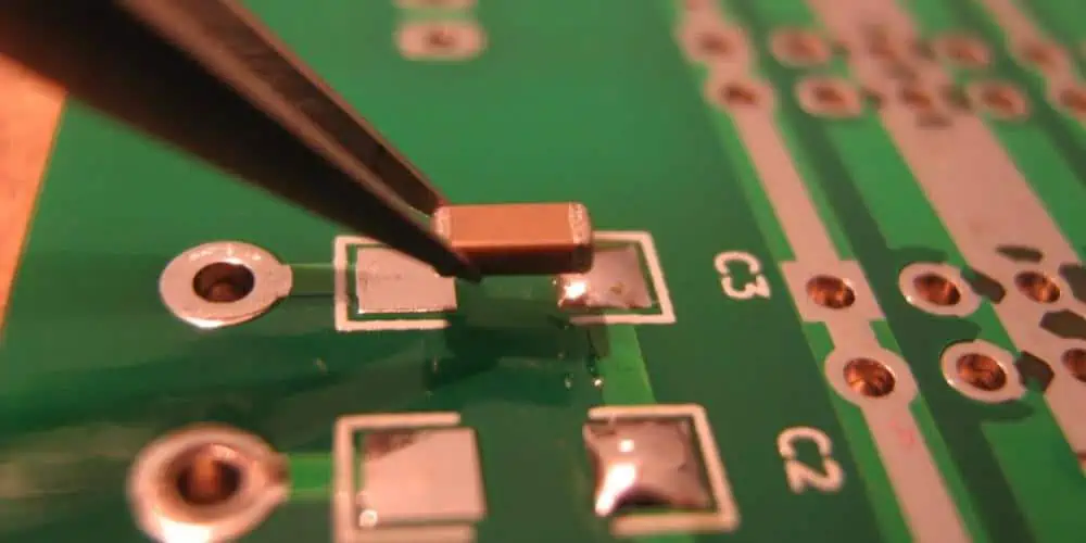
As opposed to SMD pads, non SMD pads are distinguished by the solder mask never making physical contact with its copper pad. Rather, this mask is designed to leave a space between the pad’s edge as well as the soldermask.
The solder mask is put on some copper foil to create the SMD pad, while the unmasked copper foil serves as the pad. Copper pads are larger than soldermask openings. The fine pitch component can be used with solder mask specified pads, which are frequently utilized with BGAs. Also, the solder mask usually overlaps on the top of the pcb region between the adjacent pads.
Advantages and Disadvantages of Soldermask Defined Pads
SMD pads have the following benefits:
- These pads would significantly increase the pad’s strength.
- It strengthens and increases the dependability of BGA.
- It’s a wise decision for electronic portal products.
The following are the drawbacks of SMD pads
- Worse solderability: A high temperature inside its reflow oven will influence the Solder Mask, which would also affect the solder paste’s tin area.
- Worse location of pads: Because soldermask tolerance is greater than copper tolerance, the size and placement of these pads may be affected.
- As this copper area grows, its trace area decreases proportionately and also the design of the trace becomes increasingly challenging
- Its fabrication process seems to be more challenging and demands high precision, significantly raising the cost of manufacturing
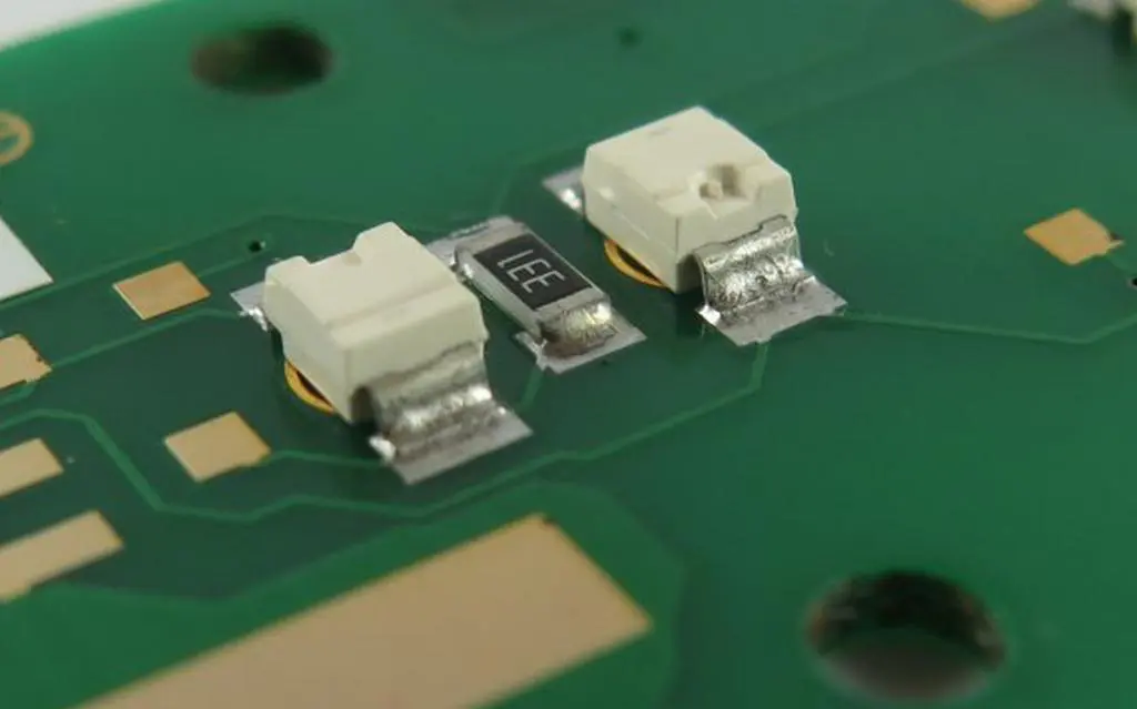
Are PCB Footprints More Than the SMD Pad Sizes?

While the size of the SMD pad you select in the PCB footprint plays a crucial role, there are additional elements to consider in the footprint to guarantee the success of the design.
- Silkscreen displaying part outlines, pin indicators, and the reference designator’s location.
- Information about the assembly layer to be included in the drawing of the PCB assembly.
- Opening of a solder mask having a PCB design rule-compliant expansion value
The opening layer of the solder mask and related clearance guidelines are crucial for avoiding DFA mistakes in design as well as subsequent assembly issues. To ensure that your board is error-free, consult the fabrication as well as the assembly team for insight on these issues.
How to Determine SMD Pad Sizes
Determining the pad size for different SMD components can be done in a number of different methods.
The component type as well as mounting method will also affect the precise determination of the pad size. For instance, leadless packages (such as QFNs) as well as leaded packages have different requirements for pad size than BGAs (such as gullwing leads or SOIC). In general, pads provide more space for the solder fillet and are bigger than component leads. IPC-7351 standard outlines these points in the manner given below.
Standard IPC-7351B
The specifications for the land patterns meant for typical components are provided by the IPC-7351B. This also gives information on calculating pad sizes. Therefore, if you wish to calculate pad sizes manually, you can go ahead.
SMD vs. NSMD Pads: What’s the Difference?
The majority of EMS providers advise using NSMD since it gives stricter control of the registration of the copper artwork in contrast to the tolerance process of its solder masking.
Additionally, the definition of the SMD pad might create stress concentration locations that, in the event of excessive fatigue, could lead to solder joint breakage.
To ensure balanced load on solder joints for NSMD, its pad sizes are often lowered by 15% more than the BGA diameter. Additionally, by using this technique, the primary layer’s routing channel may be expanded.
More information to assist you choose between NSMD and SMD for your designs is provided below:
- While utilizing non SMD pad sizes for BGA 0.4mm pitch PCB design might produce good results in small quantities, there is a good risk that low yields may occur in large quantities.
- Bear in mind that 0.4mm pitch BGA ball sizes are smaller compared to 0.5mm pitch BGA ball sizes. Further pad reduction may result in BGA pads having insufficient solderable surface. This may result in latent failures inside the field or PCBs rejected during assembly inspection.
- When employing NSMD pads to serve 0.4- as well as 0.3mm pitch BGA, bridging can occur between pads. Because there is insufficient soldermask webbing in-between the pads, bridging develops.
- The pad might come off during the reflow or during the field since the pad sizes have become so small and obviously, there isn’t soldermask webbing that can give adhesive strength.
- Ideally, there should be no trace seen between any adjacent BGA pads. They introduce shorts for external layer pitches of at most 0.4mm.
- There should only be a single trace in-between the pads on interior layers.
Conclusion
According to applicable standards like the IPC782 standard, the SMD pads for larger components (like sockets, transistors, etc.) must be adequately stretched. For example, SOT23 pads could be extended by about 0.8 to 1 mm. It will really prevent any missing solder caused by the component’s “shadow effect.” Depending on the component’s size, the size of the pad is decided. The best soldering results are achieved when the pad’s width is equal or more than or equal to the component leads’ width.