The Digital circuit design Process and its advantages

BGA Layout Tutorial

The process of developing digital circuits that can carry out a range of activities, from straightforward logical processes to intricate computational functions, is known as digital circuit design. From determining the circuit’s needs to testing and confirming the design, there are various processes involved in the design process. In this post, we’ll go over the fundamentals of designing digital circuits and give a general overview of the procedure.

Overview of Digital Circuits

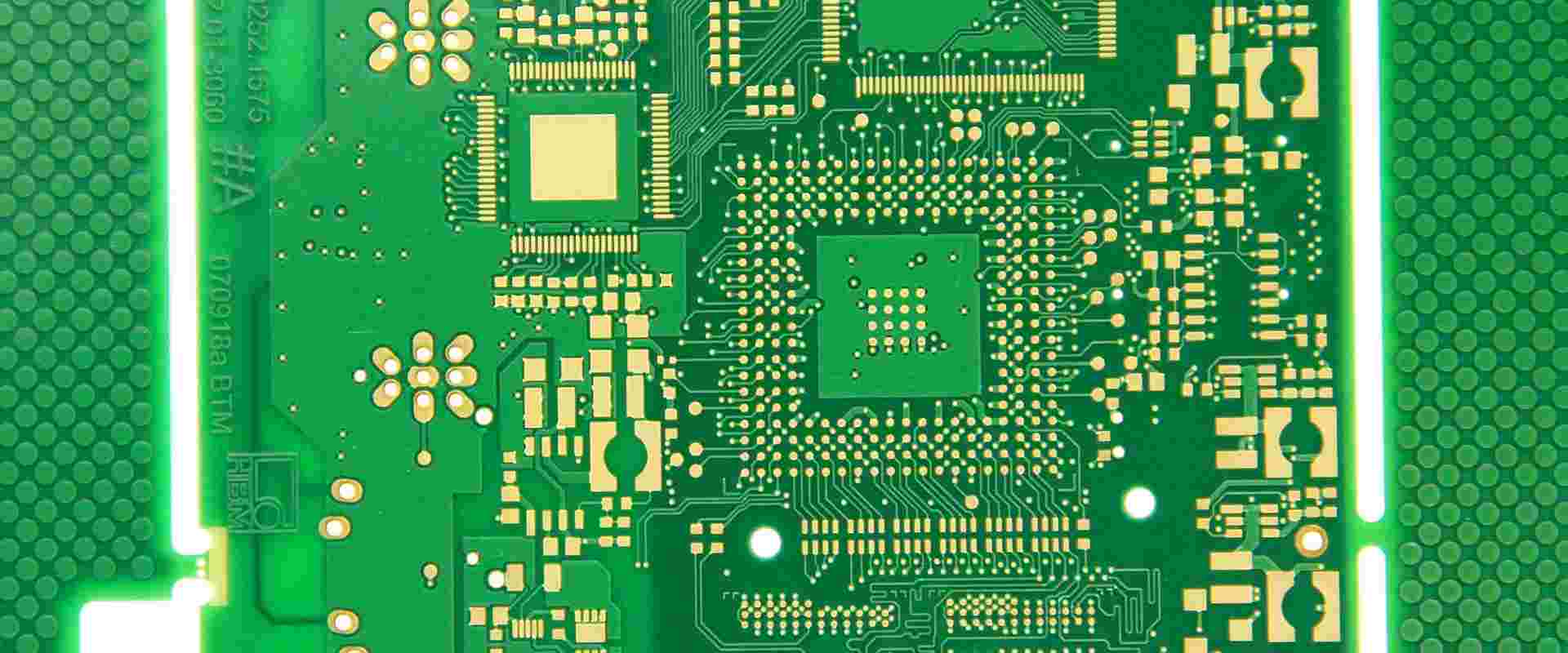
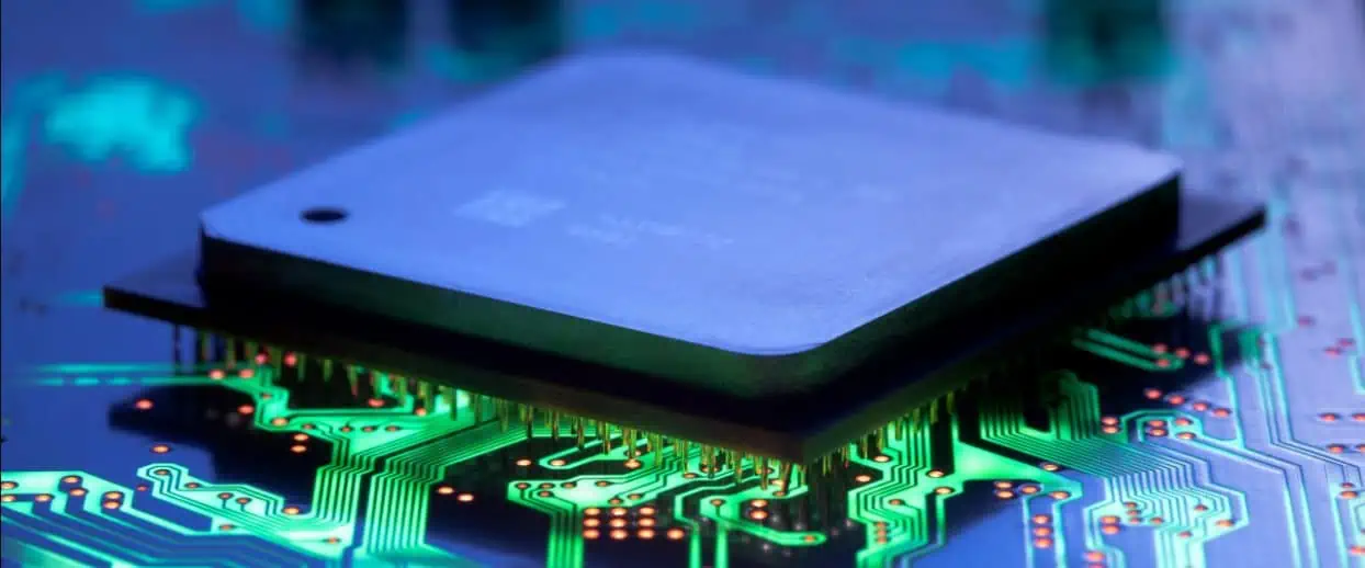
Digital circuits are electronic circuits that express information using digital signals. Because digital signals are binary, they can only have two possible values: 0 and 1. Voltage levels help express these values, with 0 normally represented by a low voltage level (for example, 0 volts) and one typically represented by a high voltage level (e.g., 5 volts). Simple logic operations like AND and OR, as well as more advanced computing tasks like arithmetic and logic operations, can be carried out by digital circuits.

Combinational circuits and sequential circuits are the two broad types into which digital circuits fall. Combinational circuits are those that generate an output solely based on the values of the current inputs. While their output solely depends on the most recent input data, they lack memory components. On the other hand, sequential circuits have memory components and generate outputs that depend on the current and past input values.

The Design Process

bare PCB layout design to cut cost

The digital circuit design process encompasses multiple steps, from determining the circuit’s needs to testing and confirming the design. However, the fundamental steps in the design process are as follows:

Requirement Analysis:

Identifying the needs of the circuit is the first stage in the design process of a digital circuit. This entails determining the purpose of the circuit and any design limitations, including a budget, power consumption, and performance standards.

Design Specification:

The next stage is to draft a design specification outlining the circuit’s specifications in great detail. The circuit’s inputs, outputs, and behavior for any possible combination of input values must all be specified.

High-Level Design:

Making a high-level circuit design comes once the design requirements are complete. This entails determining the components that will help to construct the circuit and the connections between these components to form the entire circuit. Along with the high-level design, a circuit block diagram should illustrate how the various components are connected.

Detailed Design:

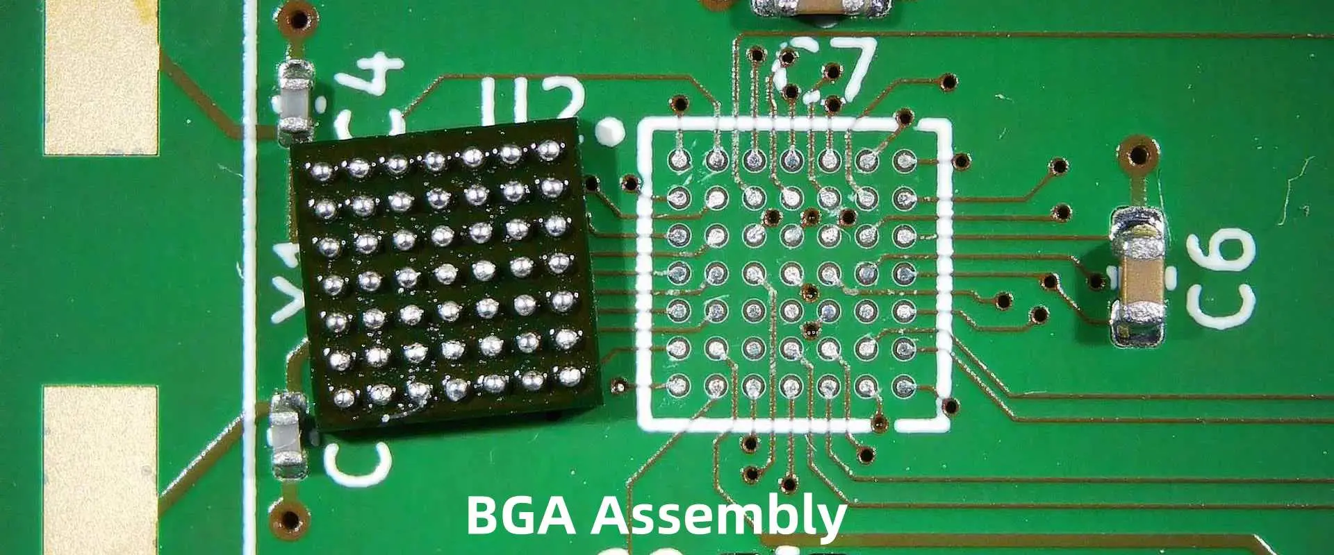
The real circuit schematic, a precise circuit diagram that displays the individual components and their connections, is created during the detailed design phase. Also, choosing the individual transistors, capacitors, and resistors that will help to construct the circuit is a part of this process.

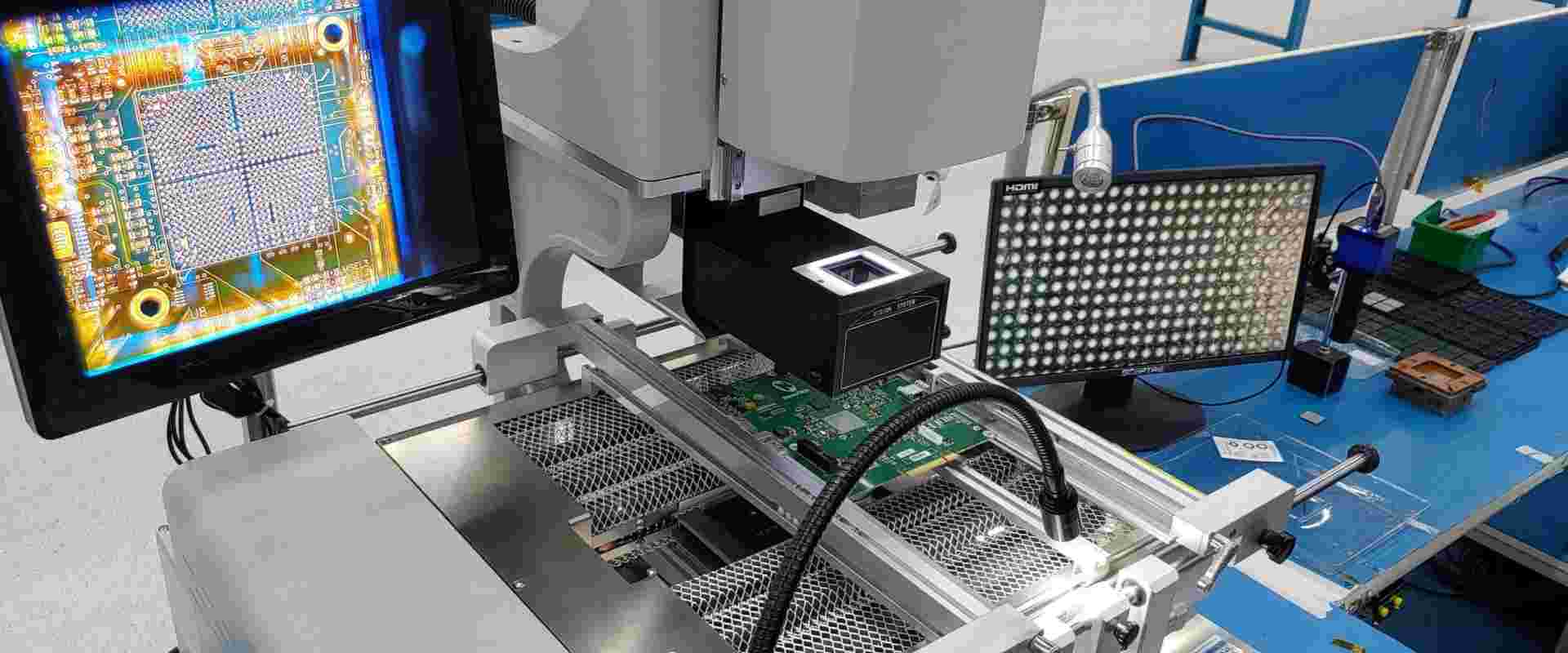
Simulation and Testing:

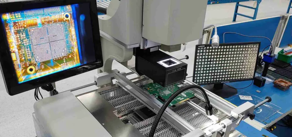
It is crucial to simulate and test the circuit design when the circuit schematic is complete to ensure it functions as intended. This entails testing the circuit under many settings, such as various input values and various ambient variables, by simulating its behavior using software tools.

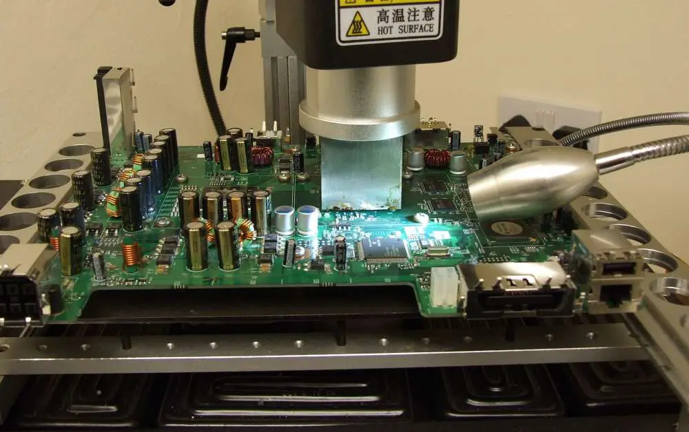
Fabrication and Testing:

When the simulation and testing process is complete, one must build and test the actual circuit to ensure it functions as predicted. Building the circuit with the chosen components and testing it in various scenarios to ensure it complies with the design specification requires doing this.

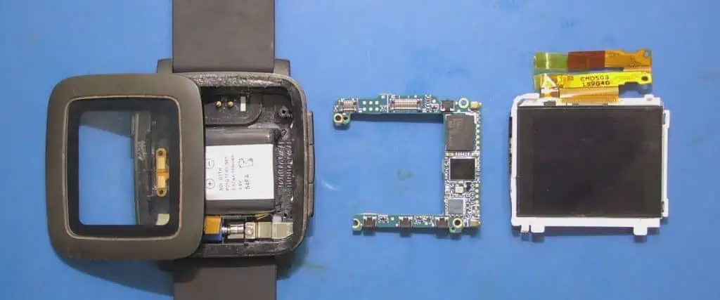
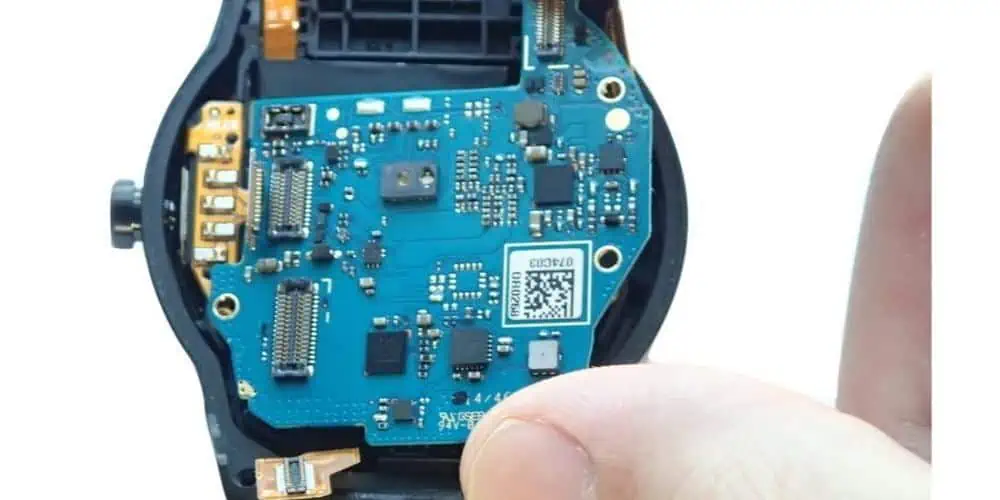
What are the main five components of a digital system?

FULL PCB MANUFACTURING Quote

These five elements combine to build a digital system capable of carrying out various tasks. The processor unit can carry out operations on the data stored in memory and carry out instructions by receiving input from input devices. The system can then communicate with other devices and systems via communication interfaces and display the results of these computations on output devices. A digital system’s primary elements consist of the following:

Communication Interfaces:

The digital system connects to other components or systems using communication interfaces. Ethernet connections, USB ports, and wireless communication technologies like Bluetooth and Wi-Fi are a few examples of communication interfaces. The digital system can communicate with other systems and devices via these interfaces to exchange information and commands.

Output Devices:

The outcomes of the computations performed by the digital system display on the output devices. The output devices might be speakers, printers, or monitors. These gadgets transform the digital signals the digital system generates into a human-friendly format.

Memory:

Data and instructions are kept in memory for the processing unit to access. In a digital system, primary and secondary memory are the two fundamental forms. As the processing unit works on them, data and instructions are temporarily stored in primary memory, commonly known as random-access memory (RAM).

Processing Units:

The component of the digital system that handles computing is the processing unit. It typically consists of a microprocessor or central processing unit (CPU), which is in charge of carrying out operations on digital data and carrying out instructions.

Input Devices:

The digital system receives input from input devices. Mice, touch screens, keyboards, and mice are a few examples of input devices. These tools let people communicate with the digital system and input data as digital signals.

Advantages of digital circuit

PCB layoutย lineย design
PCB layout line design

Digital circuits are electronic circuits that run on binary digital signals that indicate whether an electrical voltage or current is present or absent. Due to their various benefits, these circuits are essential in various electronic devices, including computers, smartphones, and televisions. Seven benefits of digital circuits are as follows:

Reduced Signal Degradation:

Signals can be transmitted over long distances by digital circuits with little signal deterioration. This is so that we can preserve the integrity of digital signals over extended distances.

Compatibility:

Since most modern electronic gadgets use digital signals, digital circuits are compatible. This makes the integration of digital circuits with other electronic systems and devices simple.

Flexibility:

Digital circuits are very adaptable since they are simple to reprogramme and reconfigure. This is so because discrete parts like easily replaceable or modifiable logic gates make digital circuitry.

Low Power Consumption:

As binary signals only have two states, they are helpful in digital circuitry, which uses less power than analog circuits. This indicates that less power is needed to change the signal’s condition.

High Accuracy:

Since binary signals clearly distinguish between the on and off states, digital circuits function with high accuracy. This enables digital circuits to carry out accurate actions with minimal error.

Easy to Store and Transmit:

Because we can represent them using binary digits, digital signals are simple to store and send. This facilitates the storage and transport of substantial volumes of data, which is essential for applications like digital processing, data storage, and communication.

High Noise Immunity:

Binary signals, which can be either high or low voltage, are used to run digital circuitry. These signals are less vulnerable to noise and interference than analog signals. As a result, the operation of digital circuits becomes more dependable and accurate.

Disadvantages of digital circuit

pcb layout design
pcb layout design

Digital circuits have several benefits over analog circuits but also have certain drawbacks. The following list of five drawbacks of digital circuits:

Propagation Delay:

Propagation delay is the time a signal takes from one point in a digital circuit to another. In applications that need high-speed or real-time processing, this delay may introduce latency or timing mistakes into the circuit.

Limited Frequency Response:

Compared to analog circuits, digital circuits are more limited in their frequency response. This is so because discrete components used in digital circuits are tuned to function at particular frequencies. As a result, digital circuits’ poor frequency response might hinder their effectiveness in high bandwidth applications like wireless transmission or digital signal processing.

Nonlinear Behavior:

Although digital circuits can behave nonlinearly, they can work with binary signals on or off. This is so because transistors, which are switching components found in digital circuits and which, occasionally behave in a nonlinear manner. As a result, unwanted harmonics, distortion, or oscillations can result from a nonlinear activity.

Limited Resolution:

Digital circuits can function at specific voltage or current levels. However, because of its low resolution, it may be challenging to measure or regulate particular parameters precisely. This is especially a problem for high-precision applications like scientific apparatus.

Complexity:

Designing and building digital circuits might be more challenging than analog circuits. This is because digital circuits consist of discrete parts, such as logic gates, which we can combine to create circuits of greater complexity. In addition, with additional gates, digital circuits get more complex, making troubleshooting and debugging more challenging.

The future of digital circuit design

Digital circuit design is a fast-developing discipline with a lot of potential for creating new electronic systems and gadgets. The following are some of the major areas that will influence digital circuit design in the future:

More Emphasis on Energy Efficiency:

Digital circuit designers emphasize energy economy as energy consumption becomes more urgent. Digital circuits’ power consumption reduces by voltage scaling, dynamic voltage and frequency scaling (DVFS), and power gating. Additionally, innovative design strategies like approximation computing will compromise accuracy for energy efficiency.

More Focus on Security:

Designing secure digital circuits is becoming more important due to the growing threat of cyberattacks. Manufacturers protect the integrity of the digital circuit by methods like secure boot and hardware security modules (HSMs), which stop unwanted access and modification. Furthermore, new encryption and authentication approaches will also increase the security of digital circuits.

More Advanced Design Tools:

As the complexity of digital circuit designs increases, designers are using more sophisticated design tools to manage the complexity and improve the performance of their circuits. For example, high-level synthesis (HLS) and artificial intelligence (AI) will automate the design process and raise the caliber of the finished design. Also, new simulation tools will make it possible to simulate digital circuits more quickly and accurately.

Higher Levels of Integration:

To make electrical gadgets smaller, cheaper, and more energy efficient, digital circuit designers are attempting to pack more functionality onto a single chip. Adopting system-on-chip (SoC) and system-in-package (SiP) architectures, which combine numerous functionalities, including processor, memory, and communication, into a single package, is helping to achieve this.

More Advanced Process Technologies:

Digital circuit designers rely on more sophisticated process methods to address the demand for more potent and energy-efficient electronic gadgets. In addition, due to their distinct electrical characteristics, novel materials like graphene and carbon nanotubes are being investigated for application in digital circuits. 

Top Examples and Applications of IIoT Manufacturing

IIoT

Industrial IoT (IIoT) refers to integrating devices, machinery, & sensors into a network that connects to the Internet. The primary objective is to gather data and perform data analysis for ongoing process enhancement. Various IIoT applications are currently available, and this new paradigm has encouraged numerous companies to adopt it to enhance productivity, optimize expenses, and increase profits. 

The IIoT market is continuously growing, with layers already implementing it. Although studies provide varying estimates of the market value of IIoT in the upcoming years, the most significant reports indicate that investment will enhance at least threefold.

It would be prudent to gain an understanding of the primary IIOT applications and also how to apply the system to gain a competitive advantage.

Applications of IIoT Manufacturing 

According to studies released by Deloitte, the corporate world places significant importance on creating IoT environments. In their “Industry 4.0” report, 94 percent of survey participants indicated that Digitalization is a crucial strategic goal for their organization. 

Although this trend is observed worldwide, in the industrial sector, companies should recognize the significance of IIoT applications in developing sustainable processes for the future.

ยท Automated & remote equipment management

One of the principal Industrial IoT ( Internet of Things ) applications is the automation of equipment management, which enables the centralized system to manage & monitor all processes of the company.

The capacity to manage equipment remotely through digital machines & software also means that it is feasible to control multiple plants situated in several geographical locations.

This endows companies with an unparalleled capability to observe the progress of their manufacturing in real-time, as well as the ability to analyze historical information related to their processes. Collecting and utilizing this data fosters an environment where informed decisions are prioritized and support the enhancement of processes.

ยท Predictive maintenance

Predictive maintenance involves identifying the requirement for machine maintenance before a crisis occurs, which could result in an urgent halting of production. Therefore, it is one of the reasons for implementing a system for data acquisition, management, and analysis. 

Among the most compelling IoT applications is a system that works through sensors installed on machines & operating platforms. These sensors can send alerts when certain risk factors emerge. For instance, sensors that monitor machines or robots submit data to the platforms, which analyze the data received in real-time and apply advanced algorithms capable of issuing warnings when parameters such as high temperatures/vibrations exceed normal limits. 

ยท Faster implementation of improvements

Industrial IoT provides valuable information to the individuals responsible for improving processes within a business model, such as process, quality, or manufacturing engineers. They can access data & analyze it more fastly and more efficiently, allowing them to make the necessary process adjustments remotely. This also speeds up the application of changes and improvements in operational intelligence & business intelligence, which offer competitive benefits to many businesses.

ยท Pinpoint inventories

Automated inventory monitoring is another important application of Industrial IoT( Internet of Things) systems. It ensures compliance with plans and alerts the relevant personnel in case of any deviations, helping to maintain a consistent & efficient workflow.

ยท Quality control

Another critical IIoT application is the capability to check the quality of products at every stage: from the raw materials used in the process to their transportation through innovative tracking applications to the response of the end client upon receiving the product.

The data collected through the monitoring of product quality at all stages is crucial for analyzing the efficiency of a company and making necessary improvements.ย Thisย includes promptly detecting any issues in the production chain and optimizing processes. Moreover, in industries like pharmaceuticals or food, where risks must be minimized, this monitoring is particularly essential.

Industrial examples of IIoT Manufacturing 

FULL PCB MANUFACTURING Quote

Many industrial giants have already embraced the Industrial Internet of Things and reported positive results. Let’s take a closer look at their expertise.

Caterpillar

In the 1990s, Caterpillar, a United States Fortune 100 company that produces heavy machinery, incorporated IIoT into its operations. It is one of the successful instances of IoT implementation in the United States. The company now has over 500,000 assets worldwide, making it the largest connected fleet in the industry.

The company implemented IIoT for predictive maintenance of machines & fleet monitoring & management, but it did not stop there. Caterpillar now produces products with built-in Industrial Internet of Things technology capabilities for its customers. For example, their excavators are considerably easy to operate than traditional ones.

Additionally, Caterpillar’s implementation of IIoT positively impacts its clients by improving equipment & machinery utilization. For example, via predictive maintenance, the company was able to save over $600,000 for one of its mining clients, while another client reported a 20% increase in productivity through the use of Caterpillar’s autonomous vehicles.

Shell 

Shell, a major global oil & gas company based in the UK and the Netherlands, successfully implemented IoT( Internet of Things) sensors in a project in Nigeria, resulting in a cost savings of over one million US dollars through continuous monitoring of oil fields. That system was designed to track the state of some pipelines, including their temperature and pressure.

During the implementation process, Shell faced challenges related to the rugged terrain of the pipeline’s location, long-distance connectivity, and scalability. However, the final solutions successfully overcame these complications.

Komatsu

Komatsu, a mining machinery manufacturer based in Japan, has reported significant improvements in Industrial Internet of Things implementation. The company has developed its own IoT(Internet of Things) system, KOM-MICS, which collects data from sensors installed on tools & robots. Thanks to a continuous flow of information, the company was able to enhance the machine operation rate by 25%.

Subsequently, with the emergence of cloud computing, the company opted for Microsoft Azure to store the information collected from the machines. This facilitated the process of expanding and integrating more machinery from their branches worldwide into the KOM-MICS system.

First-Choice for Manufacturing and Production – Shenzhen PCB

Shengyi S1190 PCB

China is the leading manufacturing country of PCB assembly. Shenzhen is considered a leading center of PCB assembly in china. Shenzhen is currently located and based in Baoan District with a center of Shajing.

The Shenzhen Printed Circuit Board assembly sector has grown quickly for more than 40 years in part because of the comprehensive local Printed Circuit Board supply chain, technological strengths, strong capital, low labor costs, and simple transportation.

In Shenzhen, there already exist over 2,000 PCB assembly enterprises. Among the many Shenzhen Printed Circuit Board assembly enterprises, some of these are PCBA producers, and some are distributors. Everyone prefers to place orders with producers directly rather than through trading firms.

Among all the Printed Circuit Board Assembly companies, some concentrate on complex assembly for industrial, automotive, commercial uses, and defense, while others concentrate on simple PCB assembly for traditional circuits, like single, double-layered PCBs and prototypes. It’s simple to order Shenzhen PCB assembly services, but you must locate a source manufacturer whose PCBA production skills match your product specifications or positioning.

Advantages Of Shenzhen PCB Manufacturing and Assembly

shengyi pcb material

There are certain reasons why Shenzhen is considered one of the leading and most favorable places for printed circuit board assembly. Among those various reasons, some are described below.

ยท Worldโ€™s Biggest Electronic Distribution Center

Huaqiang North, the largest distribution center for electronic components in the world, is located in Shenzhen.

Enterprises from all around the world that produce electronic devices buy parts from Shenzhen and then export their goods to other countries. Finding every electronic component on BOM takes one hour in Huaqiang North, but it takes around 22 hours elsewhere.

ยท Complete Shenzhen PCB Assembly Industry Supply & Support System:

A PCB manufacturing company requires supply and collaborating partners to complete the process of PCB assembly. The partners include solder paste makers, electronic component vendors, machine distributors, shipping companies, etc. 

Entire PCB assembly manufacturers, suppliers, and services may be found in Shenzhen. Moreover, Shenzhen’s PCB assembly prices are lower than those in the United States and Europe, partly because of the city’s convenient full supply chain.

ยท Experienced Shenzhen PCB Assembly Engineers

Electronics experts and professionals from around China are drawn to Shenzhen because it is a leader in electronics manufacturing and international trade. Also, Shenzhen is home to numerous industries that manufacture electronics with foreign investment. They have been around in Shenzhen for many years and have produced a large number of skilled workers and Chinese engineers in the Assembly of the PCB sector.

Additionally, the PCB assembly sector in Shenzhen is boosted by affordable labor rates and easy access to transportation. Shenzhen PCB assembly is more competitive compared to other locations worldwide as a result of these benefits.

Shenzhen PCBAs A First-Tier Choice For Production 

FULL PCB MANUFACTURING Quote

Shenzhen is also referred to as “the silicon valley of hardware,” and there is an additional term that refers to Shenzhen, which is “Shenzhen speed.” It would be wise to look for a PCB assembly supplier in China that is located in Shenzhen since this will guarantee production speed, component availability, and the least amount of delays during the PCB fabrication process. 

Speed is undoubtedly a factor to take into account while constructing a PCB assembly prototype in China. The competent, youthful, and talented engineers located in Shenzhen will work fast and effectively to complete the assembly process within hours because prototypes are typically built by hand.

Another factor to consider is that, particularly in Shenzhen, the prototype of PCB assembly in China is frequently simpler than anywhere else in the world. Prototypes only need a few components, and those parts may be bought and acquired within one day in locations like the “HuaQiangBei” tech market and also from other suppliers and manufacturers who are located in China and have stock on hand in their warehouses.

1. Labor & Professional Hands:

When you fabricate your equipment in China, you can rest easy knowing that your hardware task is in capable hands. China, and Shenzhen in particular, draws a lot of young talented engineers who want to acknowledge their dreams. These engineers frequently work in PCBA manufacturing centers to gain experience and knowledge and build better hardware-oriented expertise. Labor costs frequently have an impact on price, and PCBasic’s PCB assembly quotation is quite alluring to many international clients. China PCB manufacturing companies always work to keep costs low without compromising manufacturing quality.

2. Machinery & Equipment:

Printed circuit board assembly (PCBA) requires a certain kind of gear and equipment, which is sometimes quite expensive. PCBA in China often has access to machinery that really isn’t common but is frequently utilized in quality assurance and testing, among other advantages. PCBasic, a Chinese provider of PCB assembly, takes particular satisfaction in extensive and cutting-edge PCB equipment, which enables it to guarantee that every product leaves the workshop in flawless functioning order. It’s only one of many reasons why PCB board assembly is made in China; certain of the equipment used in PCBasic is copyrighted and private, unavailable elsewhere.

3. Sourcing Components:

It’s time to start manufacturing once you select the best facility to make your PCBA, making sure that it is well-equipped with the newest technology and equipment. To fabricate PCB arrangements in China, you will have to source various varieties of components. The majority of the componentsโ€”or their substitutesโ€”are already widely used and available on the Chinese market, so it is simple to find stock available even during times of global shortage of components. 

4. Shipping & Logistics:

It is time to deliver the manufactured product to the client when receiving a PCB assembly estimate for constructing the product in China, acquiring all the essential components and ensuring their quality, and executing all the testing required to check performance and quality. When working with PCB components, logistics and shipping are crucial stages. Particularly when working with PCB components that have special needs, like LiPo batteries as well as other parts sourced during the process of PCB assembly in China, these devices need to be packed with additional care to ensure they are delivered to the destination state safely.

The fundamental difference between COB chip and LED

COB chip

What is a COB chip?

A COB chip is a sort of packaging where several chips are put directly onto a substrate or circuit board without requiring individual encapsulation. COB stands for “Chip on Board.” COB chips typically consist of dozens to hundreds of tiny chips connected in parallel and put on a common metal or ceramic substrate.

Because of their excellent efficiency and power density, COB chips have grown in popularity recently. They are a popular option for various lighting applications since they may offer more light output with less energy use than conventional chips. Furthermore, COB chips are frequently smaller than conventional LED chips. It makes them a viable choice for applications requiring a small form factor.

The Basics of Chip on Board (COB)

A printed circuit board (PCB) is directly mounted with an unpackaged semiconductor chip using the Chip on Board (COB) method, which also requires wire bonding the chip to the PCB. Doing away with the requirement for an external package and lowering the number of interconnects results in a more reliable and compact electronic device.

The COB procedure includes the following steps:

Die Attach: A die-attach machine mounts the semiconductor chip onto the PCB. Then, the chip adheres directly to the Board using conductive adhesive or solder.

Wire Bonding: Little copper, aluminum, or gold-plated wires link the chip to the Board after mounting it. Instead, a wire bonding machine connects the wires.

Encapsulation: We apply a protective resin or epoxy to the wire-bonded chip. It protects against environmental elements like moisture, temperature, and mechanical stress.

The following are only a few advantages of COB technology:

Size and Weight: Because COB technology does not require a separate chip container, electronic products can be made smaller and lighter.

Reliability:ย COB technology removes the danger of package failure due to temperature cycling, vibration, or mechanical stress by directly connecting the analog chip to the Board.

Cost: COB technology can lower manufacturing costs because it does not require a separate chip package or interconnects.

LED lights, automotive electronics, consumer electronics, and medical equipment frequently employ COB technology.

Differences between LED and COB

FULL PCB MANUFACTURING Quote

LEDs and COBs, two separate lighting technology kinds, are widely used in several applications. However, while they have certain things in common, they also differ significantly from one another.

Chip on Board and Light Emitting Diode both go by the acronym COB. COB is a particular application of LED technology that entails installing several LEDs on a single circuit board. LED is a solid-state lighting technology that uses a semiconductor to produce light. The following are some of the main variations between these two lighting techniques:

Design and construction

The structure of LED and COB lighting is the key distinction. LEDs are tiny semiconductor chips emitting light when exposed to an electric current. Plastic packaging that helps to both protect the semiconductor from the outside elements and offer electrical connections is typically used to house them.

Contrarily, COB lighting entails directly putting several LED chips on a printed circuit board (PCB) and fusing them together via wire bonding. A phosphor film is next applied to the LEDs to create white light.

Light output and intensity

Compared to individual LEDs, COBs often produce light with a higher intensity. This is so that they can produce a focused beam of light due to the tight mounting of the individual LEDs on a COB.

Unlike the LEDs on a COB, which are close together, LEDs typically produce light with a lower intensity. Yet, they can be employed in various applications because they may be produced in various sizes and forms.

Efficiency and energy consumption

Since COBs produce more light with less energy than individual LEDs, they are often more efficient. This is due to the close mounting of the LEDs on a COB. It then lowers the energy lost as heat.

On the other hand, LEDs are less effective than COBs because they produce light of lesser intensity and are not close to each other. Though, they are still more effective than conventional lighting methods like incandescent lights.

Color rendering

In general, COBs are more precise at reproducing colors than individual LEDs. This is so because a COB’s phosphor coating generates a wider light spectrum than a single LED. Because of this, COBs are more suitable for uses like photography and art display, where color fidelity is crucial.

On the other hand, the restricted range of light that LEDs can produce can make it challenging to reproduce colors precisely. However, improvements in LED technology have made it possible to develop LEDs. They can generate a wider spectrum of light, making them more appropriate for uses where color fidelity is crucial.

Price

In general, COBs cost more than individual LEDs. This is because they require more manufacturing processes and resources. After all, they consist of numerous LEDs on a single PCB. Since cost is less of an issue, COBs are better suited for applications where strong light output and color accuracy are crucial.

On the other hand, because they are easier to make and use fewer materials, LEDs are typically less expensive than COBs. This makes LEDs more suitable for lighting in homes or businesses where cost is the main consideration.

What voltage is COB Chip?

COB LED

A COB (Chip on Board) chip’s voltage might change based on the product’s design. For example, according to the size, power rating, and intended application of the COB, COB LEDs can run at low voltage, typically between 2V to 50V.

The manufacturer’s datasheet offers details on the chip’s electrical properties like the operating voltage, current rating, and power consumption. It contains information on the voltage needs of a COB. Therefore, it is crucial to check the datasheet thoroughly to ensure the COB is compatible with the power supply and other application parts.

A constant current driver, instead of a constant voltage supply, is frequently essential for COBs to function successfully. This is so that a constant current driver can help ensure the COB receives a stable and consistent current. However, a COB’s current draw can vary based on the temperature and other external factors. Because of this, it’s crucial to choose a constant current driver that complies with the voltage and current demands of the COB chip.

COB Chip lifespan

A COB (Chip on Board) chip’s lifespan can vary based on several variables. They include the caliber of the materials used, the environment in which it operates, and the current and voltage levels it faces while in operation.

A high-quality COB chip typically has a lifespan of 50,000 to 100,000 hours or more, substantially longer than that of incandescent or fluorescent lights. As a result, even with constant use, a COB chip can last several years.

The operating temperature can also affect how long a COB lasts because too much heat will shorten the chip’s life. As a result, it’s crucial to ensure the COB properly cools. The operating temperature should stay within the manufacturer-recommended range.

It’s important to remember that a COB chip’s lifespan depends on how long it takes for its lumen output to decline by 70%. The chip may continue to produce light after this, but it will be considerably less bright.

Summary

In conclusion, the choice between LED and COB lighting technologies depends on the application’s particular requirements. Both lighting technologies offer advantages and limitations. While LEDs are ideal for applications where cost is the main consideration, COBs are ideal for those where excellent light output and color accuracy are crucial.

The future and applications of Medical Electronics Engineering

Medical Robotics Companies

Engineering and medical science combine in the specialist field of medical electronics. It entails creating tools that can treat medical issues and enhance healthcare delivery.

The health team needs biomedical engineers because they use their understanding of biology and medicine to create novel medical gadgets. For example, they aid in creating prosthetic limbs and artificial organs.

Digitalization

Designing for the automobile or healthcare sectors, in particular, increasingly emphasizes the need for digitization. The capacity to store and access data from anywhere at any time is only one of its many benefits.

Digitalization is changing how medicine is developed and made available to patients in the medical sector. It improves productivity and lowers expenses by assisting medical professionals in reaching diagnostic and treatment decisions more quickly.

Computational simulation is a crucial aspect of digitalization to determine device performance and durability for medical devices. For instance, finite element analysis (FEA) enables designers to model potential failure scenarios for medical devices.

Medical electronics engineers must also consider legal regulations, manufacturing certifications, validation standards, and concerns associated with obsolescence for obsolete or old components. This is particularly true given the increased desire for compact, sophisticated, connected devices that can meet various regulatory requirements and hit the market fast on the part of medical OEMs.

3D Bioprinting

Medical Devices PCBA

There are several uses for 3D bioprinting, such as disease modeling and drug screening. However, the most exciting is the use of 3D-manufactured organs for transplantation.

Patients may be able to print their organs using their cells or stem cells, doing away with the necessity for organ donors. In the US, there are presently about 120,000 persons waiting for a kidney, liver, or heart.

Although printing an entire organ sounds far-fetched, developments are occurring quickly. For instance, scientists at Tel Aviv University have successfully built a 3D heart from a patient’s biological components.

Robotics

We can use robots for many jobs, from moving hazardous products to providing medical treatment. For example, hospitals and clinics employ them to assist medical professionals in completing activities without jeopardizing their safety and effectiveness.

Also, these robots are employed more frequently to reduce surgical human error. They can execute precise movements and take over low-level duties while the surgeon concentrates on high-level work.

Robotics training for surgeons is another usage for them. Doctors can rehearse treatments and enhance their skills using robotic controls on simulation platforms that combine AI and VR.

Safety, quality, and efficiency are crucial elements determining how robotics will develop in healthcare. We should consider these aspects to give patients and their healthcare practitioners the greatest results.

Artificial Intelligence

A technology called artificial intelligence enables computers to learn and analyze data. Many uses exist, such as number plate recognition systems and self-driving cars.

AI assists medical professionals in the diagnosis and better monitoring and treatment of patients’ conditions. Also, it minimizes the necessity for invasive treatments and improves specialists’ decision-making.

Before they are essential in clinics and hospitals, AI solutions must overcome numerous obstacles. They include ensuring these technologies are reliable, efficient, and morally upright.

The usage of AI technology will also require training for healthcare personnel. These professionals will require the ability to evaluate data, apply it efficiently, and comprehend human-machine interaction.

Applications of Medical Electronics Engineering

FULL PCB MANUFACTURING Quote

Engineers specializing in medical electronics use their knowledge of biology and medicine to create tools that address issues with health. These tools include stethoscopes, glucose meters, pacemakers, and defibrillators.

The performance reliability of electronic medical equipment is essential because it frequently performs life-sustaining tasks. Therefore, engineers prepare for routine maintenance using parameters like mean time to failure (MTBF) and mean time to recalibrate (MTTR).

Pacemakers

An electronic device called a pacemaker monitors your heart’s rhythm and administers electricity to maintain a regular beating. Doctors treat several disorders with pacemakers, including bradycardia (slow heartbeat) and tachycardia (rapid heartbeat).

A pacemaker can help patients live longer. A pacemaker also gives beneficial medical data that can aid your doctor in choosing the right course of treatment for you.

A lead that sends electrical impulses to your heart muscle is attached to modern pacemakers and placed in the chest and belly. These leads are attached to a tiny electrical generator and a microcontroller that tracks the electrical impulses generated naturally by your heart.

The first battery-operated pacemaker was developed in the late 1950s by a Minneapolis electrical engineer called Earl Bakken and his brother-in-law, a founder of Medtronic. Manufacturers hermetically seal the lithium iodide battery to shield it from atmospheric pollution and consist of a solid electrolyte/separator.

Patient Monitoring Systems

Systems for monitoring patients’ vital signs, such as blood pressure and blood oxygen saturation, are electronic equipment. Additionally, they spot anomalies and warn clinicians when values are too high or too low.

Patient monitors come in different varieties. While some have a few options for showing various pieces of information, others can track various factors.

Health professionals can remotely monitor their patient’s vital signs using remote patient monitoring (RPM) systems, which then electronically transmit the information to them. This enhances clinical judgments made by clinicians and leads to better results.

Implants

We can replace organs and blood arteries missing from a person with medical implants. These gadgets could be electronic devices or built of biological materials like silicone, titanium, and apatite.

Patients with physical conditions like heart disease, brain injury, and deafness use implants. They can also help to monitor and manage bodily processes.

A pacemaker, which controls heart rate using microelectronics and sensors, or a cochlear implant, which can recognize and encode sound, are two common applications of implants in medical electronics engineering.

These devices are typically implanted directly into the body and are automated so that the patient does not have to activate them for them to function actively. Doing this lowers the chance of infection and protects the implant from the body’s environment.

Artificial Limbs

Amputees who have lost their natural limbs due to sickness or injury can use prosthetic limbs created specifically for them. A prosthetist, a physician, and a physical therapist create these devices to fit the patient’s physique.

Combining several materials, including metals, plastics, and carbon fibers, produces a prosthetic limb. These materials have a variety of characteristics, including density, corrosion resistance, load-bearing capacity, Young’s modulus, and strength.

Electrodes inserted in the residual limb muscles are one way to accomplish this. This enables the patient to transmit electrical signals that cause the mechanical limb’s muscles to contract.

Another strategy entails building a sensory interface that routes nerves from the natural limb to the prosthetic limb’s surrounding skin. Using a process called sensory substitution, amputees may eventually be able to experience touch with their mechanical hands.

Top 10 medical electronics engineering companies in the world

Medical PCB Assembly

Companies that specialize in designing, developing, and producing medical devices and equipment are known as medical electronics engineering businesses. These businesses play a critical part in the healthcare sector by giving medical personnel the necessary equipment to diagnose, treat, and monitor patients. The top 10 medical electronics engineering businesses in the globe according to revenue, product line, and market share include:

Siemens Healthineers

A market leader in medical technology, Siemens Healthineers offers a wide range of point-of-care testing, laboratory diagnostics, and medical imaging products and services. Siemens Healthineers is a leader in the medical electronics engineering sector, with over 50000 people and operations in over 70 countries.

General Electric Healthcare

A branch of the General Electric Company, General Electric Healthcare offers medical technologies such as imaging, diagnostics, patient monitoring, and medical software. In addition, the company provides various products and solutions to satisfy the requirements of healthcare professionals and patients everywhere.

Philips Healthcare

A division of the Netherlands multinational technology corporation Royal Philips is Philips Healthcare. The business provides various medical products and services like patient monitoring, diagnostic imaging, and healthcare informatics. With operations in more than 100 nations, Philips Healthcare is one of the world’s top engineering firms for medical electronics.

Medtronic

Medtronic, a leading medical technology provider, creates and produces equipment for various medical disciplines, including orthopedics, neurology, and cardiology. With operations in more than 160 nations, Medtronic is one of the biggest medical device firms in the world.

Abbott Laboratories

Leading healthcare provider Abbott Laboratories focuses on discovering, producing, and marketing a broad range of nutritional, diagnostic, and medicinal products. Products are available for cardiology, diabetes, neuromodulation, and other specialties from the company’s medical device division.

BD (Becton, Dickinson, and Company)

BD is a multinational medical technology provider that focuses on designing and producing diagnostic tools, lab apparatus, and medical devices. Hospitals, research facilities, and clinics are just a few healthcare environments where the company’s goods are employed.

Stryker Corporation

The Stryker Corporation is a market-leading medical technology provider focusing on designing and producing tools and devices for various medical disciplines, including orthopedics, neurology, and surgery. The business offers a wide range of products and services to satisfy the requirements of healthcare professionals and patients everywhere.

Johnson & Johnson

The pharmaceutical, medical device, and consumer health industries are all served by the multinational firm Johnson & Johnson. For example, surgery, orthopedics, and cardiovascular disease products are available from the company’s medical device section.

Boston Scientific Corporation

The research and production of medical devices for numerous medical specialties, such as cardiology, neurology, and urology, is the focus of Boston Scientific Corporation, a top medical technology provider. The company offers a comprehensive range of products and solutions to satisfy the requirements of healthcare professionals and patients everywhere.

Thermo Fisher Scientific

Thermo Fisher Scientific is a prominent biotechnology corporation with various goods and services for the analytical, diagnostics, and life sciences markets. In addition, the company’s medical device division makes products for clinical diagnostics, drug discovery, and research.

Take Control of Your Systems with the Control Box Assembly

Set-top box PCB Board

Do you need to exert control over something in your house or place of business but need help determining where to begin? Be at ease! The assembly of the control box will save the day! The control box assembly is crucial to many different devices and systems, from industrial and commercial to household ones. It is a group of pieces and elements that support the observation, management, and control of various processes. Several testing techniques are available, including point-to-point, resistance, voltage, wire position, and functional testing, to ensure the control box assembly functions appropriately. In this article, we will detail the control box assembly’s definition, parts, and testing procedures.

 Control Box Assembly: Definition

A control box assembly is a collection of parts and components that provide a way to control systems or devices. It is helpful in industrial or commercial settings but applies to residential applications. Additionally, control boxes are critical to many systems and help regulate, monitor, and control various processes.

Components of a Control Box Assembly

pcb box build assembly

A control box assembly typically has the following components:

1. Control panel:

The control panel is the main interface of the control box assembly, through which the operator may observe and manage the various operations of the system. Control panel includes indicator lights, a display screen, and a variety of input devices, including buttons, knobs, switches, and sliders. The control panel shows current information about the system’s condition, such as temperature, pressure, and power usage. It sends signals through an indicator light to the operator in case of problems such as overload or malfunction. Additionally, the operator can modify several factors using input devices, such as temperature or speed, improving the system’s efficiency.

2. Fuses:

Fuses protect the system from overloads. During the manufacturing process, designers position the fuses between the power supply and the system’s electrical components such that they will blow if the current is too high. This way, the fuse prevents the system from becoming damaged due to an overload.

3. circuit breakers

Circuit breakers are safety devices that protect the system from overcurrents and short circuits. Like fuses, they trip or open the course when the current exceeds a specific limit. However, unlike fuses, you can reset circuit breakers after tripping them, making them more convenient for many applications. Circuit breakers are commonly helpful in residential and commercial electrical systems, as well as in industrial machinery and automation systems.

4. Knobs

Knobs are input devices that allow the operator to adjust various parameters, such as temperature, speed, or volume. They consist of a rotating shaft and a pointer or indicator that shows the current setting. Knobs are helpful in household appliances, such as ovens and stovetops, and audio and video equipment.

5. Sliders

Sliders are input devices that allow the operator to adjust parameters, such as brightness or volume, by moving a lever or slider along a track. They consist of a graduated scale or indicator that shows the current setting. Furthermore, sliders commonly help in audio and video equipment, as well as in lighting control systems.

6. Switches

Switches allow the operator to turn the system on or off or to switch between different modes or functions. They have a lever or button that users can toggle or push to activate or deactivate a circuit.

Testing Methods of the Control Box Assembly

FULL PCB MANUFACTURING Quote

The following methods will enable you to verify the functionality of your control box assembly for excellent results:

1. Point-to-Point Testing:

In point-to-point testing, the engineer examines each component of a control box assembly separately. This strategy is quite helpful when there is heavy wiring of components. The engineer must, therefore, visually inspect each element and the wiring that connects it for any indications of damage or misconnected wires. In addition, a multimeter can help check the components’ connections by measuring their resistance. Before powering on the control box assembly, please do this to assist you in identifying any potential problems.

2. Resistance Testing

Resistance testing on a control box assembly assures proper operation. You start by connecting a testing device to measure the circuit resistance to the control box. By employing this method, you will quickly discover any problems or defects in the box that might prohibit it from functioning correctly.

To perform the resistance test, please link the control box to a testing setup that consists of an Ohm meter and a test lead. Next, connect the control box to the Ohm meter once you have installed the test lead. Then, using an Ohm meter, calculate the resistance of the control box circuit.

If the resistance is less than the bare minimum allowable value, the box has a problem. Many control box defects can be easy to find using the resistance test. These flaws could be corrosion, damaged connections, frayed cables, or any other fault impairing the control box’s functionality. Before utilizing the package, please correct any flaws you may have found.

3. Voltage Testing:

Voltage testing is a method for making sure the control box assembly has the appropriate voltage. Checking the voltage within the set range is essential to guarantee that the control box assembly operates correctly. Use a clamp meter or a voltage meter for this test. You will have to measure the voltage of the control box assembly using a voltage meter and compare its reading to the desired value. Please fasten the clamp meter to the cables entering and exiting the control box assembly to measure the voltage. As a result, the voltage may now be easy to measure with greater accuracy.

4. Wire Position Testing

Wire position testing helps ensure that every wire connection is accurate and that you have utilized the correct terminals for each wire. This action is crucial since improper wiring connections can lead to electrical issues and potential malfunction of the control box assembly.

Visual inspection of the wiring connections and labeling is the first step of the wire position test. Next, the technician should follow each wire to its proper terminal and reattach it if he discovers any differences. After ensuring that all wiring connections are accurate, the technician should then use a multimeter to test the resistance between each terminal and its corresponding wire.

The resistance should be within the acceptable range for the specific control box assembly. If the resistance is too high or too low, the technician should replace the wire or the terminal.

5. Functional Testing

Functional testing enables verification that the control box assembly’s design satisfies all requirements and carries out all intended functions as intended. Typically, the engineer examines the input, output, and other parts of the control box assembly as part of the functional testing procedure to ensure they comply with all the specifications.

Functional testing may be manual, automated, or a combination. Automated testing usually suits large and complicated control box assemblies, while smaller and simpler ones require manual testing. While manual tests may entail personally checking each component or functionality, automated tests may entail running scripts or programs.

Typically, engineers perform functional testing for control box assemblies by contrasting the behavior and outcomes of the control box assembly with the specification documents. Many techniques, like running simulations, doing tests in a lab setting, or even personally testing the control box assembly, can help complete this process.

Conclusion

In conclusion, a control box assembly is crucial to many systems and helps regulate, monitor, and control various processes. It comprises several components: control panels, fuses, circuit breakers, knobs, sliders, and switches. Moreover, it is essential to test the control box assembly to ensure its operation and functionality. Point-to-point, resistance, voltage, and wire position testing are methods used to detect potential problems with the control box assembly. Therefore, it is essential to maintain and regularly check your control box assembly to keep your system working efficiently.

Why You Need a Mobile IC Reballing Kit for Your Reballing Process

BGA Rework Services

We all have devices we utilize on a regular basis. For instance, most people have cars they drive frequently. Some people have jobs that need specialized equipment they would constantly use. This includes construction tools or custom-made computers.

A device that is constantly being used will need maintenance, repairing or both. Otherwise, such a device will begin to malfunction or stop working at all. This same principle is applicable to mobile phones. The IC in a mobile phone can get damaged due to constant use. Therefore, there is a need for repair. Since a mobile IC is always in constant use, it will definitely need repairs or maintenance. This repair is what we refer to as reballing.

Read further to understand the principle of mobile IC reballing. You will get to know everything about mobile IC reballing kit in this article.

What is Mobile IC Reballing?

Mobile IC Reballing Kit

IC reballing is a technique that involves repairing a faulty or damaged Integrated circuit in a mobile phone. Reballing is commonly integrated in PGA and BGA chips. Also, reballing can help to other electronic components like capacitors and resistors. The mobile IC reballing is a time consuming process that requires much effort.

If an IC has gotten damaged, reballing is often recommended to save the IC from being scrapped. There are some reasons why you have to reball an IC chip. Mobile IC repair is carried out on mobile phones. The most common reasons a mobile IC reballing is important include:

  • The mobile IC is faulty and needs to be repaired
  • The solder joint between the IC chip and a PCB have become very loose
  • You need to redo or update the IC chip since the PCB is upgraded

The Integrated circuit is a crucial component on your mobile phone. It restricts the functionality of your phone when it gets damaged. However, this component can  be fixed.

Reballing involves changing the soldered balls on an integrated circuit chip. BGA circuit design is made to have a contact between the chip and the PCB. As a result of some reasons, engineers need to recreate the ball solder joints. Reballing is a process that simply involves getting rid of old solder balls. These solder balls are then replaced with new ones.

How do you Detect a Damaged IC on your Mobile Phone

FULL PCB MANUFACTURING Quote

It is quite difficult to know if your mobile IC is damaged. However, there are some unusual things you will discover on your phone if its IC is damaged. This includes:

Heat condition

Your mobile IC is damaged if a heat contrast is with closely related IC. When your mobile phone IC unnecessarily heats up when there is a supply of voltage, then your phone is damaged.

Leaked or burnt IC

If your mobile IC has  a leaked spot or gets burnt is already damaged. You can easily locate a damaged spot by looking closely on each side of the mobile IC. A burnt IC can never work on your phone.

Open circuit

This is another reason you might have a damaged IC on your phone. Open circuit refers to any incomplete electrical circuit. Your phone IC is damaged if there is an open circuit. Open circuit usually causes a breach in the mobile IC.  If you notice an opened mobile phone IC at a point, you have a damaged IC.

Causes of Mobile IC Problems

There are various causes of mobile IC problems.

Power surge

Your IC can become irreparable if there is a high power. For example, an overrated charger can cause a power surge. An overrated charger has a greater amount of current compared to what your phone can take. Furthermore, a power surge may be as a result of your phone being struck by lightning and thunder while it is being charged. Therefore, a power surge that occurred earlier can be the reason why your mobile IC is damaged.

Moisture

This is another common cause of mobile IC damage. When your mobile phone contains moisture, this may cause a damage to your IC. Moisture occurs when water splashes on your mobile phone or when it falls into water. This could cause damage to your IC and other sensitive components of your mobile phone.

Manufacturer defects

IC problem might not happen due to your carelessness, it could be the manufacturerโ€™s fault. If your mobile phone is faulty right from the time you purchased it, there are high chances it has some IC problems.

Mobile IC Reballing Kit

bga-reballing-station

The reballing process isnโ€™t as easy as it seems. When reballing a mobile IC, there are various kinds of supplies and tools needed. The saddest part of this process is that all required supplies and tools are expensive. This is the major reason people donโ€™t carry out reballing at home.

Therefore, you will need a mobile IC reballing kit and a mobile IC rework machine. The mobile IC reballing kit is available online. These tools are what you require when carrying out a mobile IC reballing. The mobile IC reballing kit features all the necessary tools you need to reball a mobile phone IC.

The reballing process requires the use of appropriate standards, tools, and procedures. Also, the mobile IC reballing kit makes reballing much easier and faster. Furthermore, this kit offers almost everything you need for the reballing process. The price of a mobile IC reballing kit varies based on manufacturers.

Why is Mobile IC Reballing Needed?

Integrated circuits offer more durability compared to traditional arrays. However, the connection on the IC chip may become very loose as a result of exposure to harsh conditions or constituent use. A mobile IC may become damaged due to consistent use. Therefore, it is necessary to reball mobile IC to prevent malfunctioning.

The technology market needs upgradation of the mobile IC so as to keep up with the transformation. This is possible to achieve through IC reballing. Therefore, this will enhance the life span of the device. Furthermore, reballing is crucial when the motherboard needs to go through graphic chip up-gradation.

PCBs experience some heating cycles which can make a chip become unreliable. Also, heating can result in solder bridging and as such reballing comes into play. Faulty mobile IC chips needs reballing to ensure they offer optimal performance.

Some of the reasons you need to reball a mobile IC is when there are issues with the solder balls or soldering, a need to update the IC or repair a faulty IC. One easy way to get the mobile IC repaired is by replacing the damaged IC. Replacement is another option you can consider asides reballing.

You will need to desolder and solder the damaged IC using another IC. It is crucial you reball your damaged IC. However, replacement is a good option to put into consideration.

Tools Needed for Reballing

Soldering paste

Solder paste is widely integrated in the manufacturing of printed circuit boards. This paste connects electronic components to pads on the PCB. Therefore, it helps to put the electronic components in place or solder balls on the mounted area.

Solder balls

Solder balls are very crucial when reballing. These are small balls of solder scattered all over the surface of the PCB board. These balls offer contact between the printed circuit board and the chip package. Also they provide contact between stacked packages available in multichip modules.

Soldering iron

This hand instrument helps in soldering parts. It melts the solder metal and allows it to flow to the joints between the electronic components and the PCB. Soldering iron is a heated metal tip and  an insulated handle.

Desoldering wire

Desoldering wire soaks all the metal solder in a solder joint to remove all the solder present in the joint. It is also referred to as desoldering wick.

BGA rework machine

This machine supplies the necessary heat needed to remove or attach the BGA chips.

BGA chip stencil

This is a piece of metal sheet that features lots of holes for solder balls. The BGA chip stencil is made of steel. Therefore, you can heat it by using BGA machine or hot air gun to make the process of soldering easy.

BGA chip case

This is a holding stand designed for holding Chips for the purpose of reballing.

Conclusion

Since a mobile IC is always in constant use, it will definitely need repairs or maintenance. This repair is what we refer to as reballing. If an IC has gotten damaged, reballing is often recommended to save the IC from being scrapped. There are reasons why you might require reballing an IC chip.

Reballing a mobile IC can be very difficult because of the tiny fragments present in the IC. Therefore, it is advisable to hire a technician to help you with the reballing process. Reballing a damaged mobile IC isnโ€™t something you can do all by yourself. Therefore, you can hire a professional technician to help you do so.

Precision BGA Assembly Services for High-Density PCB Applications

Introduction to BGA Assembly

In the ever-evolving world of electronics, Ball Grid Array (BGA) assembly has emerged as a game-changing technology for high-density PCB applications. But what exactly is BGA assembly, and why is it so crucial in modern electronics manufacturing?

BGA assembly is an advanced surface-mount packaging technique that involves attaching integrated circuits (ICs) or other components to a printed circuit board (PCB) using an array of solder balls. These tiny spheres serve as both electrical connections and mechanical supports, enabling higher component density and improved performance.

As devices continue to shrink while demanding more power and functionality, BGA assembly has become indispensable. Let’s delve deeper into this fascinating technology and explore its impact on the electronics industry.

Types of BGAs: A Comprehensive Overview

eMMC BGA

Our state-of-the-art facility is equipped to handle a wide variety of BGA types, each suited for specific applications. Here’s a rundown of the most common BGA types we assemble:

1. Fine Pitch BGA (FPBGA)

FPBGAs feature a ball pitch of 1.00mm or less, ideal for high pin count applications in a compact area.

2. Very Fine Pitch BGA (VFPBGA)

Taking miniaturization further, VFPBGAs have ball pitches of 0.5mm or less, perfect for ultra-compact devices.

3. Thin Chip Array Ball Grid Array (CTBGA)

With a package thickness under 1.2mm, CTBGAs are the go-to choice for slim devices like smartphones and tablets.

4. Wafer Level Chip Scale BGA (WLCSP)

WLCSPs are among the smallest BGA packages, manufactured directly on the wafer. They’re commonly used in mobile devices and wearables.

5. Fan-Out Wafer Level Packaging (FOWLP)

FOWLP extends wafer-level packaging, offering higher I/O density and improved thermal performance.

6. Plastic Ball Grid Array (PBGA)

PBGAs use a plastic substrate, offering a good balance of performance, cost, and reliability for various applications.

7. Ceramic Ball Grid Array (CBGA)

Utilizing a ceramic substrate, CBGAs excel in thermal management and electrical performance, making them ideal for aerospace and military applications.

8. Tape Ball Grid Array (TBGA)

TBGAs feature a flexible tape substrate, reducing stress on solder joints in applications prone to thermal cycling or mechanical stress.

9. Flip-Chip Ball Grid Array (FCBGA)

FCBGAs combine flip-chip and BGA technologies, offering excellent electrical performance and thermal management.

10. Enhanced Ball Grid Array (EBGA)

EBGAs incorporate enhanced thermal design features, suitable for high power dissipation applications.

11. Metal Ball Grid Array (MBGA)

MBGAs use a metal substrate for superior thermal performance, ideal for high-power applications.

12. Micro BGAs

With ball pitches of 0.4mm or less, Micro BGAs are perfect for extremely space-constrained applications like wearables and IoT devices.

Learn more about:

The Compelling Advantages of BGA Assembly

bga rework process

BGA assembly offers numerous benefits over traditional through-hole and other surface-mount technologies. Here’s why it’s become the preferred choice for high-density PCB applications:

  1. Higher component density: BGAs allow for more connections in a smaller area, enabling the creation of smaller, more compact devices.
  2. Improved electrical performance: Shorter connection lengths reduce signal delays and parasitic capacitance, resulting in better high-frequency performance.
  3. Enhanced thermal management: Many BGA designs incorporate features for improved heat dissipation.
  4. Self-alignment during reflow: The surface tension of molten solder tends to align BGA components correctly, reducing misalignment risks.
  5. Reduced mechanical stress: The array of solder balls distributes stress more evenly across the package, improving reliability.
  6. Better protection of interconnections: Solder balls are hidden beneath the package, shielding them from mechanical damage and environmental factors.
  7. Simplified PCB routing: The array layout of connections often simplifies PCB routing compared to traditional leaded packages.
  8. Improved manufacturability: BGA assembly can be highly automated, leading to increased production efficiency and consistency.
YouTube video

The BGA Assembly Process: A Step-by-Step Guide

Achieving high-quality BGA assembly requires precision and attention to detail. Let’s walk through the key stages of the process:

1. Initial Design and Layout

The PCB design must account for BGA-specific requirements, including proper pad design, trace routing, and thermal considerations.

2. PCB Preparation

Thorough cleaning and inspection ensure a contaminant-free surface for assembly.

3. Baking Procedures

BGAs and PCBs are often baked before assembly to remove moisture, preventing issues like popcorning during reflow.

4. Stencil Creation and Inspection

A high-precision stencil is created for applying solder paste to the PCB, followed by careful inspection to ensure accurate apertures.

5. BGA Placement

Advanced pick-and-place machines accurately position BGA components on the PCB.

6. Reflow Soldering

The assembled PCB undergoes a carefully controlled reflow process, where the solder paste melts and forms connections between the BGA balls and PCB pads.

7. Cleaning and Inspection

After reflow, the PCB is cleaned and undergoes thorough inspection to ensure proper solder joint formation and component alignment.

Ensuring Quality in BGA Assembly: Best Practices

bga inspection

To achieve high-quality BGA assembly, several factors must be carefully controlled:

  1. Proper solder paste selection and application
  2. Accurate component placement
  3. Optimized reflow profile
  4. Controlled atmosphere during reflow
  5. Proper cooling rate after reflow
  6. Minimization of mechanical stress during handling

Verifying Solder Joint Quality: Inspection Techniques

Checking the quality of BGA solder joints is crucial for ensuring reliable connections. Here are the most effective inspection methods:

  1. X-ray inspection:ย Allows visualization of solder joints beneath the BGA package
  2. Automated Optical Inspection (AOI):ย Used for inspecting visible aspects of the assembly
  3. In-Circuit Testing (ICT):ย Verifies electrical connections and component functionality
  4. Thermal imaging:ย Can reveal issues with thermal management or inconsistent solder joints
YouTube video

Common Defects in BGA Assembly and How to Avoid Them

Despite best efforts, defects can occur in BGA assembly. Here are some common issues and tips to prevent them:

  1. Misalignment:ย Ensure precise component placement and use self-alignment properties of BGAs.
  2. Inconsistent Standoff Height:ย Control solder paste volume and reflow profile carefully.
  3. Missing Balls:ย Inspect BGAs before placement and ensure proper handling.
  4. Non-Wetted Pads:ย Use appropriate flux and ensure proper surface preparation.
  5. Bridges:ย Optimize stencil design and solder paste application.
  6. Partial Reflow:ย Fine-tune the reflow profile for complete solder melting.
  7. Popcorning:ย Implement proper moisture management procedures.
  8. Open Circuits:ย Ensure proper pad design and solder paste application.
  9. Voiding:ย Optimize reflow profile and consider vacuum reflow for critical applications.

Conclusion: The Future of BGA Assembly in High-Density PCB Applications

As the demand for smaller, more powerful electronic devices continues to grow, BGA assembly will play an increasingly critical role in high-density PCB applications. By understanding the various types of BGAs, the intricacies of the assembly process, and the key factors that influence solder joint quality, manufacturers can leverage this technology to create innovative, reliable electronic devices.

Whether you’re designing cutting-edge mobile devices, high-performance computing systems, or reliable aerospace equipment, mastering BGA assembly is essential. With the right expertise and advanced manufacturing capabilities, the possibilities for innovation in high-density PCB applications are virtually limitless.

Are you ready to take your PCB designs to the next level with precision BGA assembly? Contact our team of experts today to learn how we can help bring your high-density PCB applications to life.

What is CPU PCB? Manufacturing and Supplying

CPU PCB

Several of the electronics people use daily contain CPUs. For instance, smartphones, PCs, and other gadgets use CPU PCBs. Computer keyboards, monitors, & printers are just a few products that use CPU PCBs and microcontrollers (which incorporate CPUs).

You’ve arrived at the appropriate location if you’re looking for information on CPU PCBs. We’ve compiled a list of insightful inquiries about CPU PCBs, and we want to provide you with solutions. Let’s get started right now without further ado.

What Is CPU PCB?

The printed circuit board or PCB supports the electrical parts that power and enable the functionality of electronics. The PCB, often constructed of copper or another material that conducts electricity, is etched to permit the movement of electrical currents. Prepreg & TEFLON, among other non-conductive materials, comprise the PCB’s basis.

A CPU PCB is a circuit board that acts as a platform for a computerized device’s central processor (CPU) and controllers. Moreover, these PCBs feature industry-standard architecture, modular PC cards, and peripheral component connection (PCI) (ISA). Different standards, such as the PCI extended for instrumentation cards (PXI) and the extended embedded technology classification, are added (ETX).

Designing A CPU PCB

FPGA vs. GPU vs. CPU

The CPU Pcb design differs significantly from conventional PCB design in several ways. When designing the CPU PCB, especially when using multilayer boards, other processes must be followed. We will describe the procedure for creating a CPU PCB using multilayer boards in the following section.

Choose The Component Mounting Technology

Surface and through-hole mounting are the two main techniques for attaching components to a PCB. Components are mounted to the Board using surface mounting via an automated process. To fit the components, through-hole technology, on the other hand, involves drilling holes inside the PCB foundation. The decision of which approach to take for a particular design is based on some variables and design considerations.

Determine The Microcontroller

The microcontroller, which is the main element of the CPU PCB, must be carefully chosen to satisfy the demands of the application. To guarantee the best possible performance of the CPU PCB, it is crucial to select a microcontroller with the correct performance requirements, including overclocking speed.

USB To Serial Converter

The CPU needs to communicate with the computerized system to function. To help translate the signals from the CPU to the automated process through a USB port, an additional chip is needed. On the microcontroller, the signal can be retrieved using synchronous serial peripherals like UART.

Analog To Digital Peripherals

When converting an analog signal into digital signals and enhancing overall usefulness, choosing the suitable analog-to-digital signal converter was essential. It’s crucial to thoroughly analyze and choose the converter that is best suited for the particular application.

CPU PCB grounding techniques

Grounding PCB Techniques 

FULL PCB MANUFACTURING Quote

Grounding is vital in PCB design; therefore, following the correct grounding procedures is necessary for the best results. The following are crucial pointers to remember regarding grounding for PCB design.

1. Ensure Everything Is Attached

Scrutinize your PCB layout to make sure there are no loose components. Consider covering open spaces with copper or vias that link to the ground plate for the best performance. This strategy will lay out a clear path for effective signal transmission to the ground.

2. Keep Ground Layer Whole

On a specialized ground layer, which is frequently found in four-layer boards, make sure there are no route traces. Avoid breaking up the ground layer by adding route traces to prevent producing a ground current loop. Instead, make sure the ground layer is intact.

3. Have a Common Ground Point

It is advised to have a central position where all grounds converge to provide a good grounding in a PCB. A specific layer of the board or the product’s metal chassis can be used for this purpose. Because the conductors radiate from this entry point in the shape of a star, it is often referred to as a star ground. To preserve signal integrity in mixed-signal systems, separate analog and digital power sources may be necessary, as well as separate analog or digital grounds that join at the star point.

4. Minimize the Use of Series Vias

Reduce the number of vias in your ground routes and ensure that component grounds are connected directly to a ground plane to avoid impedance and voltage differentials. Impedance can be increased by adding extra vias to the board, which is crucial to consider for fast transient currents that may result in voltage differentials all along the impedance path.

5. Design Grounding Before Routing

Before beginning any routing process, it is critical to design a ground structure. It’s critical to ensure the ground is adequately planned because it is the foundation for routing. While problems with one signal not functioning as planned may not significantly impact, poor grounding might represent a serious risk to the entire system.

6. How Currents Are Flowing

Understanding the current flow on a circuit board can help ensure proper grounding. It is crucial to consider the signal’s final destination and matching return path. Since the outgoing and returning signal pathways contain the same currents, they can affect the power stability and occurrence of ground bounce.

7. Dynamic Variance B/W Grounds

Consider the possibility of dynamic differences while connecting the ground between several systems’ boards. When working with applications that make use of long-distance wires, this becomes even more crucial. Optical isolators, reduced voltage differential signals, or common-mode chokes can all be utilized to keep the variations in check.

8. Mixed-Signal Considerations

When working with both analog and digital on a board, careful planning is required. It’s crucial to separate the digital parts from the analog sections, including the analog-to-digital converter topologies (ADCs) or digital-to-analog converters. To achieve this, the ADC’s grounds can be connected and linked by a standard ground pin, allowing digital signals to travel to other areas of the PCB.

What is the Significance of Smartwatch IoT?

Smartwatch IoT

Sportspeople and those who wish to get in better physical shape have grown to rely on connected watches as well as activity trackers as their “indispensable” companions. These advanced devices gather a lot of information about our movements, activities, and vital signs (age, weight, sex, sleep cycle, heart rate, etc.).

Based on our activity, they could be linked to a variety of external sensors that add extra information. Smartwatches are typically connected to a platform for data storage that enables users to see, analyze, as well as share their actions. The security of these items is a major problem given the type of data they connect.

What Does a Smartwatch Mean?

A wearable computer that strongly matches a wristwatch and other timepiece devices is called a smartwatch. Several smartwatches are known to be bluetooth-capable and can tell the time. The watch transforms into a bluetooth adaptor that may bring the features of the smartphone towards the timepiece.

The interface of the watch can be used by the wearer to make and take phone calls via their mobile device, read text and email messages, obtain weather information, play music, compose text and email messages, and communicate with a digital assistant.

Some smartwatches are separate gadgets that provide a particular function. For instance, certain smartwatches gather information regarding the user’s health, such as tracking the user’s heart rate. Others give the wearer driving or walking directions using GPS information.

What Functionalities are available on Smartwatches?

Smartwatch IoT Device

Smartwatches come with a lot of functions. These include the following:

  • Healthcare informatics like level of blood oxygen, temperature and blood pressure monitoring, and heart rate
  • Calling and messaging capabilities akin to those found on the smartphone
  • For emergency calls if the wearer falls
  • Social media as well as other notifications gotten from synchronized mobile apps
  • Games, photos, music, as well as other entertainment alternatives
  • Location capabilities like maps, compass, and an altimeter
  • GPS tracking

In most cases, smartwatches connect to the user’s smartphone. The watch has many of similar functions and software programs as the phone and can sync with it. Users of Apple Watch must also own any Apple iPhone.

Smartwatch Types

There are several all-purpose smartwatches available on the marketplace which offers a range of capabilities. Some examples of this are as follows:

  • Apple’s all-purpose smartwatch is the Apple Watch
  • There are numerous companies that create and market timepieces using the Wear OS of Google.
  • Samsung’s exclusive smartwatch OS is used by Tizen watches.

Smartwatch IoT Use Cases

If you always keep your smartphone nearby when you’re out as well as about, you’ve certainly encountered a circumstance where you only glanced away briefly before realizing that you had missed a very important message or call.

You can receive notifications right away by using a connected watch or smartwatch to connect to the smartphone. You should be conscious of the smartphone even if it is only close and examine it occasionally. Instead, you wouldn’t have to be concerned about missing any of these important detail because you will be informed just by wearing one.

Get top-notch health management features

These watches come with features that make it simple for users to maintain their health. Apps that assess the heart rate as well as those which record the path you take when exercising are common examples. Health-conscious folks who regularly cycle or run find these features to be quite appealing.

Similarly, some apps allow you to track your sleep, which is seen as a wonderful feature for people who are concerned about the biological clock.

Easily assess the weather

FULL PCB MANUFACTURING Quote

There are definitely instances when you do not really feel like unlocking your smartphone only to assess the weather using an app because mornings are typically busy.

You can effortlessly check the weather with connected watches and smartwatch IoT coupled with performing your morning tasks.

Serves as mobile wallet

Every year, the number of people adopting a wearable payment device increases. You can leave the house with no credit card or cash and make purchases with your wristwatch by downloading the app for mobile payments. It makes using public transportation simple and enables you to stop by any store while out for quick run or stroll even though your wallet isn’t with you.

Playing music

You may stream as well as play music if you own a connected watch or smartwatch. You can do it with some devices even if you don’t have a smartphone. When you wish to run while listening to music but are unable to bring your smartphone along, they are useful.

Easily set an alarm on your wristwatch with your smartphone

One feature that makes people utilize these watches is the alarm feature. By linking it to a smartphone, you may quickly set up an alarm. When using a smartphone and paying attention to something, you could miss the alarm going off. Yet with these watches’ vibrating alarms, you wouldn’t have to stress about it anymore. When you’re concentrating on work or catching a nap, this popular feature is helpful.

Experience effortless time conversion when traveling overseas

While traveling abroad, changing the time on your device might be a hassle. Immediately you get there, you ought to verify the time and manually change it.

Even when you’re traveling abroad, you won’t need to worry about connected watches and smartwatch IoT because all you need to do is set the location, then the watch would automatically change to the local time.

What are the Advantages of the Smartwatch IoT?

Smart watch IoT

Below are a few key aspects of wearable IoT

Better management of health

When smart wearables first came out, the only health-related features were step counts and the heart rate monitor. A smartphone or other portable device would receive the data gathered by a smart wearable and organize your fitness regimen based on your BMI.

With the convergence of smartwatches and the internet of things, a variety of useful applications are feasible:

  • Monitoring a baby’s crib continuously to provide prompt attention to a toddler;
  • Enhancing patient-centric healthcare through data streaming in real time of vital signs.
  • Make emergency care for the elderly easier.
  • Depending on the person’s health, the smartphone app may even provide reminders to drink water.

Navigation and communication

Certain smartwatches have built-in communication features, and you can add a SIM card to connect them straight to the Web. The feature is ideal for using a GPS or SatNav while traveling. Pets could be fitted with smart wearables to help in tracking them. A smartphone is not necessary thanks to the built-in calling and texting capabilities of some smartwatches.

The smartwatch already established itself as a helpful covert tool thanks to its built-in cameras. Some smartwatches offer elderly patients emergency treatment. They can summon the help of their caregivers or some emergency services such as hospitals by simply tapping or clicking the screen. Certain smart devices can also monitor babies; they can let you know if the child is weeping or doing fine.

Device management

Also, the IoT ecosystem is accessible through the smartwatch. Your smartphone as well as a number of other gadgets are connected to it. You might receive a vibrating or sound alarm if you leave your cell phone behind and move beyond a certain range. Certain smart devices even allow you to locate a missing phone. Some devices additionally include a remote control feature, which helps in deleting or encrypting data or lock your phone permanently.

What is the Future of the Smartwatch IoT?

Smart watch PCB Board

In the past 50 years, smartwatches have seen many changes. Complex data regarding the wearer can now be tracked, stored, and transmitted by them.

Biometric data is one area on which several smartwatch manufacturers have been concentrating. Smartwatches can track fitness data such as daily steps as well as body composition. Also, they can keep an eye out for prospective medical issues. The goal of manufacturers is to increase the number of health-related technologies that can be incorporated into smartwatches.

 The increased prevalence of chronic diseases that demand ongoing monitoring is one factor contributing to the focus of healthcare. In this regard, smartwatches are beneficial. In addition, the smartwatches are helpful for recognizing COVID-19 exposure as well as contact tracking thanks to their integrated GPS, health, as well as mobility characteristics.

With better real-time access to the health data of a patient, medical professionals may offer more individualized care and spot ailments before they worsen.

Conclusion

As we learnt, A wearable computer that strongly matches a wristwatch and other timepiece devices is called a smartwatch. You can track your GPS locations, keep an eye on your fitness levels, and read text messages faster thanks to smartwatch IoT. The best part is that the majority of the gadgets that let us accomplish this are portable and hands free, so you don’t need to pull them out of your pockets.

Several of the aforementioned pieces of information could be acquired prior to wearables, but doing so sometimes needed hassles and inconvenient technologies.