In the PCB industry, there are standards guiding the design, manufacturing, as well as assembly of circuit boards. Creating standards is a good way of ensuring the functionality and safety of circuit boards. Therefore, manufacturers must adhere to these standards. There are several standards in the PCB industry and each standard is created for a particular purpose.
One of the most popular standards in the PCB industry is the IPC standard. The Institute of Printed Circuits (IPC) was created to help PCB manufacturers develop better and functional electronics. IPC standards focus on all aspects of PCB production and as such these standards are of different types. The IPC 6011 is a popular standard manufacturers adhere to. Our main discussion here focuses on the IPC 6011 and what aspects of PCB manufacturing it covers.
The IPC 6011 standard is a guideline that provides the requirements for the production of circuit boards and as well outlines the functionality and quality they meet. These standards cover all aspects of PCB production from design to assembly and testing, inspection, and even documentation.
The IPC 6011 standard describes three main class definitions, which indicate quality level from the lowest to the highest. It should be noted that the degree of inspection is the difference in these classifications.
The major classifications are:
IPC 6011 Class 1 Electronics: This classification describes the manufacturing standard of general electronics products like toys. Also, computer and computer parts. These products don’t have much effect on our daily lives. They are ideal in applications where there is no much importance attached to cosmetic imperfections.
IPC 6011 Class 2 Electronics: The class 2 electronics classification covers Dedicated Service Electronics Products like televisions or other home appliances. In some ways, these electronic products have less impact on our lives. IPC 6011 Class 2 electronics are more critical than Class 1. Robust computers and communication equipment are a good example of class 2 devices.
IPC 6011 Class 3 Electronics: This is the third classification which describes the High-Reliability Electronics Products like aerospace and medical devices. These devices have a major impact on our lives. For instance, medical devices are used for life saving purposes. If these devices fail, human lives and a lot will be at stake.
Human lives could be at risk when parts or components of aerospace devices fail. Therefore, there is no room for error in devices like this. In products like this, there is no tolerance for downtime. Flight control systems or life support machines must function as required.
What do these Class Definitions Really Mean?
The three classifications of devices based on the IPC standards points out the severity of defects that can be allowed in a circuit board. While some defects can be tolerated in class 1 electronics Class 3 can’t tolerate some manufacturing defects. If a circuit board has many defects or extreme issues, such a board won’t be categorized as a class 3 board. The defects will disqualify the ranking of the board as Class 3.
A good number of manufacturers produce their circuit boards to meet up with the IPC standards. Sometimes, it all depends on checking a board for defects and grouping it in the right class. Although most PCB manufacturers try to produce quality and reliable boards, you need to specify the class of PCB you want. This is because some PCB manufacturers don’t have the necessary equipment that meets the standards of class 3 PCBs. In some cases, the performance of a board might meet the criteria for a class 2 board.
If such happens, your board will yield more and this will help you save more when you opt for a Class 2 board. However, if the application for which a board will be used is mission-critical, then a class 3 board is an appropriate choice. Ensure you have a proper discussion with your contract manufacturer about the type of PCB class your electronics project requires.
There are many defects found in a circuit board. The IPC standards have a list of defects they have specifications for. Some of these defects can affect performance while some are cosmetic and will definitely have no effect on reliability or performance.
Annular rings
The IPC 6011 standard specifies the center of the hole and the ring’s width around the hole. A Class 1 ring can have 189 degrees breakout while Class 2 allows for 90 degrees breakout. For Class 3 rings, the IPC specifies its minimum measurement at 0.050 mm around the hole. The specifications for each class differs.
Solder Joints
The solder coverage for joints is specified by the IPC 6011 standard. This indicates how well you should use solder to wet the lead in the via . There is no specification for Class 1 since it is a general electronics product. On the other hand, Class 3 and Class 2 require 270 degrees and 180 degrees respectively.
Component misalignment
This is another defect specified by the IPC. A good number of SMT components experience tombstone or overhanging of the solder pad. The IPC made some guidelines for component overhang. For Class 1 and Class 2 PCBs, there should be less than 50% of pad width while that of Class 3 should be below 25% pad width.
According to the IPC 6011 PDF, other defects specified include non-wetting, electromagnetic issues, acid traps, and interoperability.
In some scenarios, no specifications are detailed for Class 1, but there are different guidelines for defects for both Class 2 and Class 3. Sometimes, the three classes have similar requirements for a particular defect.
You should note that the IPC PCB classification could be very complex and electronic manufacturers need to choose the appropriate class for their board. However, manufacturers need a proper understanding of the requirements of each standard so as to know what to go for. Also, they must be aware of the associated manufacturing considerations of these boards.
Conclusion
IPC 6011 standard helps manufacturers to adhere to certain guidelines concerning the production of printed circuit boards.
PCB has always been a leading industry that has supported different domains out there. Therefore, we are able to use our consumer electronics without any fear in the long run due to the incorporation of these PCBs.
There is no doubt that the PCB industry has a strong position in different regions. Just like we have PCB Georgia, where this field houses a huge workforce that makes the challenging development of electronics an easy take. We are going to take a look at the techniques and work styles that the state of Georgia follows for PCB production in detail.
The geographical position of a state matters a lot when we are considering PCB production. There are many reasons for it. The state is located at the junction of Europe and Asia. Due to this reason, it is able to connect both continents and proves to be a smooth pathway for PCB trading between both regions. It not only establishes an unbreakable connection between the trading routes and PCB supply between both continents but transportation through Georgia is also much more feasible for European and Asian suppliers.
· Skilled Workforce
Georgia is one of the leading states which depends on a huge technical workforce and highly skilled professionals associated with PCB production. Due to this reason, states like Georgia are able to produce sufficient PCBs to meet the fluctuating market demands on all counts. The workers successfully implement their technical knowledge in the PCB operations so that seamless production of PCBs can take place each time.
· Supportive Business Environment
Another plus point of Georgia is that it supports budding PCB marketers and entrepreneurs in an impressive way. Businesses that are in the PCB industry can avail much of Georgia’s benefits because of its supportive business atmosphere. More investments can take place, especially within the PCB industry. Business-friendly policies, taxation, and more business opportunities make it a good choice for entrepreneurs on all counts. There is no doubt that native and foreign investors are taking great interest in taking full advantage of Georgia’s supportive business atmosphere as well.
· Infrastructure and Industrial Zones
Georgia is also favorable for businesses because of its huge industrial zone and infrastructure. The part that Georgia’s infrastructure plays in the fortification of the PCB industry is highly important. Warehouses, storage facilities, and other amenities offered by the industrial zones of Georgia are attractive to other investors willing to establish themselves in this region. You will also find special industrial parks that provide feasibility for doing business and making business operations easier for PCB producers at the same time.
· Technological Advancements
Georgia is also leading in technological advancements so that it can intrigue future investors. Besides, it is also crucial for revolutionizing PCB operations with the help of technology and reducing the margin of error to a great extent. Automation and SMT, along with tech-based inspection techniques provided by Georgia to the producers, have certainly made a difference for the PCB producers. All these features come together to develop highly precise and functional PCBs for clients.
· Collaborative Ecosystem
The collaborative ecosystem in Georgia is the backbone of PCB producers out there. The state not only practically supports the producers but also trains and educates them so that they can perform better than before in the long run. From research facilities to testing labs, a budding producer can gain crucial insightful knowledge for doing feasible PCB business. This collaborative system of Georgia is beneficial in terms of bringing ideas into reality and achieving impossible tasks. It also instills the sense of doing something bigger and better for the country without pulling the legs of the business rivals.
· Export Opportunities
This state has also become a leading contributor to IT and PCB exports for the country. The reason is that it is a mini hub that cultivates the sense of incorporating technology for farming new and better systems to make PCB production much easier. The annual exports made by Georgia alone are impressive to invest in it so that a producer can take full advantage of its technological zones and IT parks at the same time. If you’re looking to step up on PCB exports, then there is no better place than Georgia.
There is no doubt that Georgia offers so much to PCB producers, and therefore, you can invest in this region without any fear as well. Below we are going to quickly overview the top PCB companies that are active in Georgia so that you can have a vivid idea about its industrial potential on all counts.
1. Sanmina Corporation:
Sanmina Corporation is an important PCB producer in Georgia which specializes in different PCB services for its clients. It delivers designs, prototypes and handles urgent bulk PCB production on all counts. They have been delivering exceptional PCB solutions to their clients coming from different technical domains. From automotive to aerospace and telecommunications, you can find your PCB solutions with Sanmina Corporation easily.
2. Kimball Electronics:
Kimball Electronics is an old player in Georgia when it comes to performing outstandingly for its clients. They are remarkable in PCB services. Due to this reason, their clients are availing benefits from their PCB testing systems, quick product completion, and flawless PCB assemblies. They are considerable because they never compromise on quality, and it shows in their products and PCB types as well. Besides, they are also good in flawless OCB assemblies when needed. They have a stellar portfolio. Due to this reason, they are always able to attract new clients to try their services.
3. Advanced Circuits:
Advanced Circuits is another Georgian company that gives tons of PCB services that you can try. They are your one-stop solution to PCB needs. The reason is they provide different services like bulk production. They pass their PCBs through stringent quality control systems to make sure they are ready to use.
4. TT Electronics:
TT Electronics is also operational in Georgia, and they deal with global PCB brands and interested clients. They offer a huge range of services that you can try. They are experts in the development of different PCBs ranging from simple to complex. Moreover, their PCBs are exceptional in performance, and they serve well in terms of application performance and longevity. From medical to aerospace and defense, they deliver PCBs to all technical domains out there.
5. GES Electronic & Service:
GES Electronic & Service has been functional in Georgia for many years. They are dependable in terms of high-quality PCBs, industrial prototypes, and delivering PCBs within a deadline. From assembly to development and delivery, you can rely on them for all of your PCB needs. They are also experts in different types of circuits. That’s why they are able to address so many clients on a regular basis. Their PCB solutions are effective in various technical fields as well.
6. Sunstone Circuits:
Sunstone Circuits is important to consider because they are experts in quick turn prototypes assembly pcb. You can check their online platform, where you get all the necessary insights regarding PCB production and assembly, along with PC designs as well. Due to this system, their clients are able to interact with their associates 24/7 in their time of need.
7. Epec Engineered Technologies:
Epec Engineered Technologies is an outstanding PCB manufacturer in Georgia. Also, have won the trust of several clients in the past years. This made it possible for them because of the exceptional PCB services and products they offer. Their PCB designs are flawless, and prototypes help them with PCB development without any complications later. They have a good reputation in the market. Because of their reliable and durable PCBs that serve different technical fields as well.
Conclusion:
There is no doubt that Georgia is a dream destination for PCB investors because it has a bright future for them. From business opportunities to a collaborative system for entrepreneurs, the state of Georgia remarkably provides you with all the basic amenities to proceed with your operations without any blockades.
Prototypes are the initial sets of designs of a product. They are produced to enable the checking of the product’s functionality and to verify if there is a need to make changes – and where?
There are two major types of electronics prototyping. These are:
PCB Prototyping: this has to do with the production of the initial sets of designs of the electronic products’ aspects.
Electronic Product Prototyping: this deals with the design and overall functionality of the final electronic product to be produced.
It is important to get the steps correctly when doing electronic prototype manufacturing. The abidance by these guidelines is a surefire way to make the initial designs of the electronics and be able to figure out how best to address any design-related issues.
Note that the prototypes are not entirely wholistic, as they are often based on the development stages. For example, a Printed Circuit Board (PCB) in the early stages of development wouldn’t use a similar prototype method as the one that is nearing completion.
With these points in mind, let us talk about some of the types or categories of electronic board prototypes.
1. Proof-of-Concept (PoC) Prototype
This electronic prototype manufacturing process comes after the initial review or requirement survey of the electronic product – where the quality of the data or information about the product is filtered.
As soon as the requirement survey stage is completed, the next process is the Proof-of-Concept (PoC) prototype. This has to do with the early-stage validation process, whereby the concept of the electronic product is evaluated.
These are some of the reasons why this prototyping type is relevant:
It aids the validation of the technical feasibility or usability of the electronic product, when it is finally ready to be shipped into the market.
The Proof-of-Concept (PoC) concept also allows for the proving of the electronic product’s fundamental concept, as well as correlating that to the affordability of the product.
This prototype type allows for the provision of answers to some fundamental questions, such as the basic solution option. This also allows for the figuring out of the possibility of the final/finished electronic product to solve the intended problem.
2. The “Works-Like” Electronic Prototype
This refers to the first set of initial processes of creating electronics, based on functionality. Thus, the function of the works-like prototype is to help determine the functionality of the electronic product, with a particular focus on the internal electronics or components.
As a production-level of the electronics production, the works-like prototype helps to specify the following:
The development of a Printed Circuit Board (PCB)
The usage of the created circuit board to hold and connect all of the discrete electronic components used by the electronic product.
3. The “Looks-Like” Prototype
This type of prototyping electronic board has to do with the appearance or the possible finish of the electronic product. This is why it is also called the appearance prototype.
The goal here is to separate the likely presentation or appearance of the final product from how that electronic product is meant to function (works-like).
To that end, the following are obtainable when an electronic product undergoes the looks-like prototyping process:
The process focuses on the optimization of the finishes, material, user experience, aesthetics, look, feel, color/CMF, and form of the electronic product.
Always use an ideal prototyping technique when making the looks-like electronic product prototypes.
What is the Best Prototype Technique for “Looks-Like” Prototypes?
When making or producing the looks-like prototypes, you are usually presented with an array of options. You can choose to go through the olden/conventional methods of using clay or foam or upgrading to the latest techniques.
Here is a summary of all the common techniques used to produce the looks-like prototypes:
a. Clay Techniques
This technique helps you to get a feel or an idea of what the final product will feel like in the users’ hands.
These are some of the benefits:
Starting out with this technique could drastically reduce the number of iterations or corrections you need to make to the prototype, when you upgrade to using the 3D model.
The clay prototyping technique is very helpful in the products targeted for use in the automotive industry.
b. Foam Prototyping Techniques
You can use these to quickly and cheaply transfer an electronic concept into something you can hold in your hands.
In addition to being affordable, these techniques are also commonly used by the consumer product designers.
c. 3D Printing Techniques
These techniques are based on the use of additive prototyping processes to add materials for the creation of the desired shape.
The 3D printing techniques cover the following:
Selective Laser Sintering (SLS)
Fused Deposition Modeling (FDM) and;
Stereolithography (SLA)
d. Computer Numerical Control (CNC) Machining
This is the opposite of the 3D printing technique, in the sense that it is a subtractive process, as opposed to the addictive process tenable to the 3D printing method.
To this end, using the CNC machining prototyping technique involves the removal of materials from the prototype, to enable the creation or formation of the desired shape.
This technique is also prioritized or preferred over the 3D printing technique due to the flexibility. This means that you can use a plethora of materials in this technique, such as specific plastic resins, plastics and metals.
This is the point of prototyping an electronic product, whereby the combinations of looks-like (appearance prototype) and the works-like prototype is required.
The engineering prototype is also called:
EP and;
Alpha Prototype
Minimum Viable Product (MVP)
This prototyping type involves:
The fusion of the looks-like and works-like prototypes to create an appearance or electronic product outlook that closely resembles the final product.
The proximity to having a final (working) product, with the exception of testing the production and preparing the same for mass productions.
At this stage, the electronic product or device will perform the key or primary functions, but with the exception of the secondary functions, the modules and the features.
A combined effort between the industrial designer (who finetunes the aesthetics and form of the device), and the mechanical engineer (who integrates the device into the plastic shell or housing).
It is important to mention that the alpha prototyping stage is also a medium for the electronic product/device owners to kickstart a series of early-stage fundraising rounds. This is the stage when the product can be shown to investors and customers alike.
5. Beta Prototyping
This is the stage where the rough ends of the electronics prototyping are smoothened. During the beta prototyping stage, the focus is to ensure that the product or device has had the general design optimized for the Design for Manufacturing (DFM).
These are some of the beta prototyping processes:
The goal is to build a fully-functional prototype, devoid of flaws.
However, some design-related flaws/errors are still noticeable, but would be fixed before the certifications for the device/product are obtained.
Up to 50 units of the device or product are made at this stage. Silicon molding is the common method used for this purpose.
The units are sent for different certifications, such as RoHS, UL, Bluetooth SIG, CE, and FCC.
The prototyping process also involves the use of engineering analysis to evaluate the following: tolerance, structural optimizations and thermal simulations.
These are some of the testing procedures used during the beta prototyping of electronic devices/products:
Engineering Validation Testing (EVT): this is used to test up to 50 units of the electronics to ensure that they meet the functional requirements, as dictated in the Product Requirements Document (PRD).
Design Validation Testing (DVT): as the name signifies, this is used to validate the product’s design, as it pertains to the cosmetic and environmental specifications. The types of tests used here include waterproof, submersion under water, abrasion, burning, and dropping from a particular height.
Production Validation Testing (PVT): this comes on the hinges of the establishment of an official production run. The PVT testing process requires the usage of the actual production tooling to establish a pilot production line. The goals include ensuring that zero issues are on the production line and that the inefficiencies in the production line are removed. The PVT also focuses on the confirmation of the workers’ understanding of the product assembly process.
6. Pre-Production Prototype
Congratulations if you got to this stage of electronics prototyping. The pre-production prototype stage is the closest you can get to having a final product that the customers will see and which has been certified error-free.
It also involves the following:
The elimination of the design-related errors or problems.
The certification that the device or product works as intended.
Making of components used for setting the quality control standards and the quality acceptance standards, ahead of the product’s mass production.
The optimization of the product for manufacturing.
Conclusion
The process of making electronic products or devices ideal for final production starts with prototyping.
You can use the Proof-of-Concept (PoC) prototype to validate the concept of the product, the works-like prototype for validating the possible performance of the final product and the looks-like prototype to get an overview of the final product’s appearance or outlook.
The engineering prototyping aids the creation of a product that resembles the final product, while the beta prototyping helps you to optimize the product according to the specifications of Design for Manufacturability (DFM).
Once these are in place, you can then proceed to the pre-production prototype stage to eliminate all the flaws, ensure the product’s performance, and get the iteration readied for mass production.
After spending 18 years designing circuits for everything from consumer gadgets to 77GHz automotive radar modules, I can tell you that material selection has never been more critical than it is right now. The explosion of 5G infrastructure, autonomous vehicles, and AI-driven data centers has fundamentally changed how we think about PCB materials. What worked five years ago simply won’t cut it for today’s high-speed, high-frequency designs.
This comprehensive guide compares the major PCB materials and brands available in 2026, with real specifications you can use in your next design. Whether you’re working on a cost-sensitive consumer product or a mission-critical aerospace system, understanding your material options is the difference between a successful product launch and months of redesign cycles.
Understanding PCB Materials: Why Your Substrate Choice Matters
The substrate you choose affects virtually every aspect of your board’s performance. It determines signal propagation speed, insertion loss, thermal behavior, and even long-term reliability. I’ve seen projects fail not because of bad circuit design, but because someone spec’d standard FR-4 for a 10GHz application where it simply couldn’t maintain signal integrity.
PCB materials serve three fundamental purposes: they provide mechanical support for components, electrical insulation between conductive layers, and thermal management for heat-generating devices. The challenge in 2026 is finding materials that excel in all three areas while remaining cost-effective and manufacturable.
Key Properties That Define PCB Material Performance
Before diving into specific brands and products, let’s establish the parameters that matter most when evaluating PCB materials for your application.
Dielectric Constant (Dk) measures how much electromagnetic energy a material can store. Lower Dk values mean faster signal propagation, which is why high-speed designs favor materials with Dk values between 2.2 and 3.5 rather than standard FR-4’s 4.2 to 4.8 range. For a given impedance target, lower Dk materials allow wider traces, making fabrication easier and more consistent.
Dissipation Factor (Df), also called loss tangent, indicates how much signal energy converts to heat as it travels through the dielectric. This is arguably the most critical parameter for high-frequency designs. Standard FR-4 with Df around 0.020 becomes practically unusable above 5GHz, while advanced materials with Df below 0.002 maintain signal integrity well into millimeter-wave frequencies.
Glass Transition Temperature (Tg) marks the point where a laminate transitions from rigid to soft. Standard FR-4 sits around 130-140°C, which caused massive problems during the lead-free transition when reflow temperatures jumped to 260°C+. High-Tg materials at 170-280°C are now standard for any design requiring lead-free assembly or exposure to elevated operating temperatures.
Decomposition Temperature (Td) indicates when the resin system begins breaking down irreversibly. For automotive and aerospace applications where reliability is paramount, Td values above 340°C provide the necessary margin for repeated thermal cycling.
Coefficient of Thermal Expansion (CTE) describes how much the material expands when heated. Mismatched CTE between the laminate and copper can cause via failures and pad lifting during thermal cycling. Z-axis CTE is particularly important for thick multilayer boards with many via connections.
Search 0+ materials from top manufacturers worldwide
Showing 0 materials
Manufacturer
Part Number
Type
Dk
Df
Tg
Td
Material Type Legend
Standard FR-4High-Tg FR-4High-Speed DigitalRF/MicrowaveFlexibleMetal Core
Key Properties
Dk – Dielectric Constant
Df – Dissipation Factor (Loss Tangent)
Tg – Glass Transition Temperature
Td – Decomposition Temperature
CTE – Coefficient of Thermal Expansion
UL 94 – Flammability Rating
Compare Materials
Property
FR-4: The Industry Workhorse Still Going Strong
Despite all the advances in specialty materials, FR-4 remains the dominant PCB substrate for good reason. It’s affordable, universally available, and well-understood by every fabricator on the planet. The key is understanding where FR-4 works and where it doesn’t.
Standard FR-4 Applications and Limitations
Standard FR-4 with Tg around 130-140°C works perfectly for consumer electronics, industrial controls, and any design operating below 1GHz without extreme temperature requirements. The material costs roughly $0.10-0.50 per square inch and offers predictable performance with virtually no lead time concerns.
The limitations become apparent in three scenarios: high-frequency operation, high-temperature environments, and lead-free assembly with multiple reflow cycles. If your design hits any of these criteria, you need to look at enhanced FR-4 variants or specialty materials.
High-Tg FR-4: The Stepping Stone to Performance
High-Tg FR-4 variants with Tg from 170-180°C bridge the gap between standard materials and expensive specialty laminates. Products like Isola 370HR (Tg=180°C, Dk=4.04, Df=0.021) and Shengyi S1000-2 (Tg=170°C, Dk=4.25, Df=0.016) handle lead-free assembly without the cost premium of high-speed materials.
I specify high-Tg FR-4 for automotive ECUs, industrial motor drives, and power electronics where thermal performance matters but signal integrity requirements stay modest. The 20-30% cost premium over standard FR-4 is well worth the improved reliability.
FR-4 Material Comparison Table
Material
Manufacturer
Dk @1GHz
Df @1GHz
Tg (°C)
Td (°C)
Best Application
Standard FR-4
Various
4.4-4.7
0.018-0.022
130-140
300-310
Consumer electronics
370HR
Isola
4.04
0.021
180
340
High-reliability multilayer
S1000-2
Shengyi
4.25
0.016
170
340
Lead-free assembly
IS410
Isola
3.97
0.020
180
350
High-layer count
NP-170
Nan Ya
4.30
0.017
170
335
Cost-effective high-Tg
KB-6165
Kingboard
4.25
0.016
170
340
Volume production
VT-47
Ventec
4.20
0.018
175
340
Automotive, industrial
High-Speed Digital Materials: Meeting the 112G PAM4 Challenge
The data center buildout and AI compute explosion have pushed SerDes speeds to levels that seemed impossible just five years ago. Designing for 56G NRZ was challenging enough; now we’re routinely working with 112G PAM4 signaling where every tenth of a dB in insertion loss matters.
Panasonic Megtron Series: The High-Speed Standard
Panasonic’s Megtron family has become the default choice for high-speed digital designs in networking and computing. The materials process like FR-4 but deliver electrical performance approaching PTFE, making them the sweet spot for cost-conscious high-speed applications.
Megtron 4 (R-5725) serves as the entry point with Dk of 3.8 and Df of 0.005 at 1GHz. It works well for designs up to 10Gbps and costs roughly half what premium low-loss materials command. I use it for consumer networking gear and industrial Ethernet applications where performance matters but budgets are tight.
Megtron 6 (R-5775) represents the current workhorse with Dk of 3.71 and Df of 0.002 at 1GHz. This material handles 56G PAM4 signaling comfortably and remains the go-to choice for data center switches and AI accelerator boards. The processing compatibility with standard FR-4 means fabricators don’t need special equipment or procedures, keeping costs reasonable.
Megtron 7 (R-5785) pushes performance further with Dk of 3.37 and Df of 0.0015 at 1GHz. For 112G PAM4 designs with long traces, this material provides measurably better eye diagrams than Megtron 6. The cost premium of roughly 30% over Megtron 6 is justified for critical high-speed links in next-generation switches and HPC systems.
Isola High-Speed Portfolio
Isola offers a comprehensive range of materials spanning from enhanced FR-4 to ultra-low-loss laminates, giving designers flexibility to optimize cost versus performance.
FR408HR represents Isola’s enhanced epoxy solution with Dk of 3.68 and Df of 0.0092 at 1GHz. At roughly half the cost of Megtron 6, it works for designs up to 25Gbps with reasonable trace lengths. The material also offers excellent thermal performance (Tg=190°C) making it suitable for demanding environments.
I-Speed drops loss further with Dk of 3.63 and Df of 0.006, bridging the gap between FR408HR and premium low-loss materials. It’s become popular for mid-range networking equipment and storage systems operating at 25-50Gbps.
I-Tera MT40 enters ultra-low-loss territory with Dk of 3.45 and Df of 0.0031. For 56G and 112G PAM4 applications, this material competes directly with Megtron 6 and often wins on price for volume production.
Tachyon 100G represents Isola’s flagship with Dk of 3.02 and Df of 0.0021. The material enables 100G+ Ethernet with minimal signal degradation and sees extensive use in hyperscale data center equipment and AI/ML server interconnects.
High-Speed Material Comparison Table
Material
Manufacturer
Dk @1GHz
Df @1GHz
Tg (°C)
Max Data Rate
Relative Cost
FR408HR
Isola
3.68
0.0092
190
25 Gbps
1.0x
Megtron 4
Panasonic
3.80
0.005
175
10 Gbps
0.8x
I-Speed
Isola
3.63
0.006
180
50 Gbps
1.3x
Megtron 6
Panasonic
3.71
0.002
185
56 Gbps
1.5x
I-Tera MT40
Isola
3.45
0.0031
215
112 Gbps
1.8x
Megtron 7
Panasonic
3.37
0.0015
200
112G+
2.0x
Tachyon 100G
Isola
3.02
0.0021
215
112G+
2.2x
RF and Microwave Materials: Rogers, Taconic, and Beyond
When frequencies climb above 5GHz and into the millimeter-wave spectrum, even the best epoxy-based materials struggle. This is where ceramic-filled and PTFE-based laminates from Rogers, Taconic, and others become necessary.
Rogers Corporation: The RF/Microwave Leader
Rogers has dominated the high-frequency laminate market for decades, and their materials remain the reference standard for RF and microwave designs. The company offers multiple product families targeting different frequency ranges and performance requirements.
RO4000 Series combines ceramic-filled hydrocarbon resin with woven glass reinforcement to achieve low loss while maintaining FR-4-compatible processing. This family has become the default choice for commercial RF applications where PTFE’s processing challenges aren’t justified.
RO4003C (Dk=3.38, Df=0.0027 at 10GHz) works for frequencies up to 6GHz and processes with standard FR-4 lamination cycles. RO4350B (Dk=3.48, Df=0.0037 at 10GHz) adds UL 94 V-0 flame retardancy while maintaining similar electrical performance, making it the material of choice for RF power amplifiers and base station equipment.
RO3000 Series uses PTFE with ceramic filler to achieve lower loss than the RO4000 family while maintaining reasonable CTE for multilayer construction. RO3003 (Dk=3.00, Df=0.0013 at 10GHz) has become the standard for 77GHz automotive radar modules where both performance and high-volume manufacturability matter.
RT/duroid Series represents Rogers’ ultra-low-loss PTFE products for the most demanding aerospace and defense applications. RT/duroid 5880 (Dk=2.20, Df=0.0009 at 10GHz) delivers the lowest loss available but requires specialized processing and bonding techniques for multilayer construction.
Taconic: The Cost-Effective RF Alternative
Taconic offers competitive alternatives to Rogers materials, often at lower price points with comparable performance. For cost-sensitive RF applications or when Rogers materials face availability constraints, Taconic provides excellent options.
TLY-5 (Dk=2.20, Df=0.0009 at 10GHz) directly competes with Rogers RT/duroid 5880, offering similar ultra-low-loss performance for satellite and phased array applications.
RF-35 (Dk=3.50, Df=0.0018 at 10GHz) provides an alternative to Rogers RO4350B for commercial RF designs. The ceramic-filled PTFE construction offers excellent thermal stability and processes more easily than pure PTFE materials.
CER-10 (Dk=10.0, Df=0.0025 at 10GHz) addresses applications requiring high dielectric constant for size reduction, such as GPS patch antennas and other miniaturized RF circuits.
Isola RF Solutions
Isola has expanded beyond high-speed digital into RF/microwave with materials that bridge the gap between their epoxy-based products and pure PTFE laminates.
Astra MT77 (Dk=3.00, Df=0.0017 at 10GHz) targets 5G mmWave and automotive radar applications with ultra-low loss combined with standard processing compatibility. This material has gained significant traction in the 77GHz automotive radar market as an alternative to Rogers RO3003.
RF/Microwave Material Comparison Table
Material
Manufacturer
Dk @10GHz
Df @10GHz
Process Type
Best Application
RO4003C
Rogers
3.38
0.0027
FR-4 Compatible
Commercial RF to 6GHz
RO4350B
Rogers
3.48
0.0037
FR-4 Compatible
Power amplifiers, base stations
RF-35
Taconic
3.50
0.0018
FR-4 Compatible
Commercial RF, filters
Astra MT77
Isola
3.00
0.0017
FR-4 Compatible
5G mmWave, automotive radar
RO3003
Rogers
3.00
0.0013
Modified
77GHz automotive radar
TLY-5
Taconic
2.20
0.0009
PTFE Process
Aerospace, defense
RT/duroid 5880
Rogers
2.20
0.0009
PTFE Process
Phased arrays, satellite
CER-10
Taconic
10.0
0.0025
FR-4 Compatible
Miniaturization, patch antennas
Flexible and Rigid-Flex PCB Materials
The push for smaller, lighter electronics has driven explosive growth in flexible and rigid-flex PCB technology. Wearables, medical implants, drones, and even smartphones now rely on flex circuits to achieve form factors impossible with rigid boards alone.
DuPont Pyralux: The Flex Standard
DuPont’s Pyralux family has dominated the flex PCB market for decades, offering materials for virtually every application from consumer electronics to aerospace.
Pyralux AP all-polyimide construction (Dk=3.4, Df=0.002 at 1GHz) provides the highest reliability for applications requiring extreme flex life and temperature resistance. Medical devices, aerospace, and military systems typically specify AP materials despite the cost premium.
Pyralux LF uses acrylic adhesive (Dk=3.6, Df=0.020 at 1GHz) for cost-sensitive applications where moderate flex performance suffices. Consumer electronics and standard flex interconnects commonly use LF materials.
Pyralux TK combines fluoropolymer with polyimide (Dk=2.9, Df=0.002 at 1GHz) for high-speed and RF flexible circuits. This material enables flex designs operating at frequencies where standard polyimide would cause unacceptable loss.
Pyralux HT targets high-temperature applications above 200°C, such as under-hood automotive and EV battery management systems where standard flex materials would degrade.
Choosing the right PCB material requires matching material properties to application requirements. Here’s how I approach material selection for common design scenarios.
5G Infrastructure and mmWave Applications
5G base stations and mmWave equipment demand materials with ultra-low loss at frequencies from 24GHz to 77GHz. The combination of high frequency and outdoor deployment creates a challenging environment.
For sub-6GHz 5G, Megtron 6 or I-Tera MT40 provides adequate performance at reasonable cost. The digital baseband section can use these materials while only the RF front-end requires specialized laminates.
For mmWave frequencies (24-77GHz), Rogers RO3003 or Isola Astra MT77 become necessary. These materials maintain stable Dk and low loss at millimeter-wave frequencies while offering sufficient thermal stability for outdoor enclosures.
Automotive Radar and ADAS Systems
Automotive radar operates at 77GHz, requiring materials that maintain performance across the -40°C to +125°C automotive temperature range. Beyond electrical performance, automotive applications demand materials meeting AEC-Q200 qualification and IATF 16949 manufacturing standards.
Rogers RO3003 has become the de facto standard for 77GHz automotive radar front-ends. The material’s stable Dk across temperature ensures consistent radar performance regardless of ambient conditions.
For radar baseband and processor sections, high-Tg FR-4 or materials like FR408HR provide adequate performance at lower cost. Hybrid stackups combining Rogers materials for RF layers with epoxy-based materials for digital layers optimize the cost-performance tradeoff.
AI Servers and High-Performance Computing
AI training clusters push data rates beyond 100Gbps over long backplane traces, creating unprecedented signal integrity challenges. The heat density of GPU-heavy systems adds thermal management complexity.
For 112G PAM4 interconnects, Megtron 7 or Tachyon 100G provide the ultra-low loss necessary for acceptable eye diagrams at 20+ inch trace lengths. The materials’ high Tg also helps manage the elevated temperatures in densely packed AI servers.
Hybrid stackups using Megtron 6 or Megtron 7 for high-speed signal layers with standard high-Tg FR-4 for power and ground planes reduce cost while maintaining signal integrity where it matters most.
Material Selection by Application Table
Application
Frequency Range
Data Rate
Recommended Materials
Key Requirements
Consumer Electronics
DC-1GHz
<1 Gbps
Standard FR-4
Low cost
Industrial Controls
DC-1GHz
<1 Gbps
High-Tg FR-4
Temperature stability
Automotive ECU
DC-5GHz
1-10 Gbps
FR408HR, Megtron 4
AEC qualification
Data Center Networking
DC-30GHz
25-56 Gbps
Megtron 6, I-Tera MT40
Low insertion loss
AI/HPC Servers
DC-40GHz
112G PAM4
Megtron 7, Tachyon 100G
Ultra-low loss
5G Base Station (Sub-6)
0.4-6GHz
25+ Gbps
Megtron 6, RO4003C
Mixed RF/digital
5G mmWave
24-39GHz
25+ Gbps
Astra MT77, RO3003
Stable Dk, low Df
Automotive Radar
77GHz
N/A
RO3003, Astra MT77
Temperature stability
Aerospace/Defense
1-40GHz
Various
RT/duroid, TLY-5
Highest reliability
Hybrid Stackups: Optimizing Performance and Cost
One of the most effective strategies for managing PCB material costs is using hybrid stackups that combine different materials in a single board. The concept is simple: use expensive low-loss materials only where they’re needed and specify cost-effective materials everywhere else.
Practical Hybrid Stackup Examples
A typical 16-layer high-speed design might use Megtron 6 for the top four layers carrying high-speed differential pairs, then transition to standard high-Tg FR-4 for power, ground, and low-speed signal layers. This approach can cut material costs by 40-50% while maintaining signal integrity on critical nets.
For RF/digital hybrid designs like 5G base stations, the RF section might use Rogers RO4350B while the digital section uses Megtron 6 or FR408HR. Proper transition design between material regions is critical, but fabricators experienced with hybrid builds handle this routinely.
Hybrid Stackup Cost Comparison
Stackup Type
Configuration
Relative Cost
Signal Integrity
All FR-4
16L High-Tg FR-4
1.0x
Baseline
All Megtron 6
16L Megtron 6
2.5x
Excellent
Hybrid
4L Megtron 6 + 12L High-Tg FR-4
1.6x
Very Good
All Tachyon
16L Tachyon 100G
3.5x
Outstanding
Hybrid Premium
4L Tachyon + 12L Megtron 6
2.2x
Excellent
Design Considerations for Specific Materials
Each material family has processing quirks that affect design rules and manufacturing yield. Understanding these considerations before design completion prevents costly redesigns.
FR-4 Design Guidelines
Standard and high-Tg FR-4 materials are the most forgiving to design with. Most fabricators maintain extensive design rule documentation for FR-4 processes, and capabilities continue improving.
For best results with FR-4, specify tight weave glass styles (1080, 2116) to minimize fiber weave effect on high-speed signals. Consider specifying spread glass or very low profile copper for designs above 10Gbps where weave-induced skew becomes measurable.
High-Speed Laminate Considerations
Megtron, I-Tera, and similar materials process like FR-4 but benefit from tighter fabrication tolerances. Work with your fabricator to ensure they have experience with your specific material choice.
Copper roughness significantly affects loss at high frequencies. Specify HVLP (hyper very low profile) or RTF (reverse treated foil) copper for high-speed signal layers. The smoother copper surface reduces conductor loss and improves insertion loss performance by 0.5-1.0 dB/inch at 25GHz.
PTFE and Rogers Material Guidelines
Rogers RO4000 series materials process similarly to FR-4, but pure PTFE materials like RT/duroid require specialized handling. PTFE’s low surface energy makes adhesion challenging; plasma treatment is often required before copper plating.
For multilayer PTFE designs, discuss bonding film options with your fabricator. Some designs use Rogers bonding films while others use thermoplastic polyimide or PTFE adhesive films depending on performance requirements.
Avoid back-drilling PTFE materials if possible; the material’s softness can cause tear-out. If back-drilling is necessary, work with fabricators experienced in PTFE processing to optimize drill parameters.
IPC Standards and Material Specifications
Understanding IPC standards helps communicate material requirements clearly and ensures you receive consistent product from fabrication.
Key IPC Specifications for PCB Materials
IPC-4101 defines qualification and performance specifications for base materials. The standard uses “slash sheets” to categorize materials by their properties. For example, /21 denotes standard FR-4 while /126 covers high-Tg multifunctional epoxy.
IPC-4103 covers materials with specialty functions including high-frequency laminates. Rogers and other specialty materials are typically qualified to this specification.
IPC-4202 addresses flexible base dielectrics, covering the polyimide and other films used in flex circuit construction.
Common IPC Slash Sheet Reference
Slash Sheet
Material Type
Typical Tg
Example Products
/21
Standard FR-4
130-140°C
Generic FR-4
/24
Mid-Tg FR-4
150-170°C
Various
/26
High-Tg FR-4
170-180°C
Isola 370HR
/99
Ultra-high Tg
>200°C
Isola 185HR
/126
High-performance multifunctional
180-200°C
FR408HR
/129
Low-loss high-speed
180°C+
Megtron 6
Cost Optimization Strategies for PCB Materials
Material costs can represent 30-60% of bare board fabrication costs for specialty materials. Strategic decisions during design can significantly reduce these costs without sacrificing performance.
Design for Material Efficiency
Keep board sizes within standard panel dimensions to minimize material waste. Work with your fabricator to understand their panel sizes and optimize your board dimensions accordingly.
Consider material utilization when specifying exotic materials. A single prototype using Tachyon 100G might require purchasing an entire panel, driving per-board costs sky-high. For prototypes, consider slightly de-rated materials that are more readily available.
Volume Considerations
Material pricing drops significantly at volume, but minimum order quantities vary widely. Rogers materials often require full-panel minimums, while Megtron and Isola products may be available in smaller quantities.
Establish relationships with fabricators who maintain inventory of common specialty materials. Fabricators serving the networking and telecom markets typically stock Megtron 6, FR408HR, and RO4350B, enabling faster turns and better pricing.
Useful Resources and Database Links
For detailed material specifications and selection assistance, the following resources provide authoritative information:
Regional PCB Material Suppliers: Beyond the Big Names
While Rogers, Isola, and Panasonic dominate discussions about high-performance PCB materials, several regional suppliers offer competitive alternatives worth considering, especially for cost-sensitive applications or when facing supply chain constraints.
Chinese PCB Material Manufacturers
China’s PCB materials industry has matured significantly over the past decade. Companies like Shengyi Technology and TUC (Taiwan Union Technology) now produce materials that compete directly with Japanese and American products in many applications.
Shengyi Technology has become the world’s largest copper-clad laminate manufacturer by volume. Their S1000-2 high-Tg FR-4 sees extensive use in automotive and industrial applications, while their SF305 ultra-low-loss material targets data center and 5G infrastructure. For cost-sensitive designs where absolute performance isn’t critical, Shengyi products often deliver 20-30% cost savings compared to equivalent Isola or Panasonic materials.
TUC (Taiwan Union Technology) has developed a strong position in high-speed digital materials. Their TU-872 (Dk=3.45, Df=0.0035) competes effectively with Megtron 6 for data center applications. The company’s close relationship with major Taiwanese PCB fabricators ensures good availability and technical support in that manufacturing ecosystem.
EMC (Elite Material Co.) focuses on high-speed and RF materials with products like EM-890 (Dk=3.40, Df=0.0032) that target 100G+ applications. Their materials have gained traction in Asian networking equipment manufacturing.
European and Other Regional Options
Ventec offers a range of materials from standard FR-4 through high-speed laminates. Their tec-speed 6.0 (Dk=3.65, Df=0.0055) provides a cost-effective option for mid-range high-speed designs. Ventec’s European presence and local technical support make them attractive for European OEMs concerned about supply chain resilience.
Nan Ya Plastics and Kingboard dominate the standard and mid-range FR-4 market with massive production capacity. For high-volume consumer and industrial applications where basic high-Tg FR-4 suffices, these suppliers offer excellent pricing and consistent quality.
Regional Supplier Comparison Table
Manufacturer
Region
Strength
Key Products
Price Position
Shengyi
China
Volume, cost
S1000-2, SF305
Budget
TUC
Taiwan
High-speed digital
TU-872, TU-768
Mid-range
EMC
Taiwan
Ultra low-loss
EM-890, EM-891
Mid-range
Ventec
Global
Broad portfolio
VT-47, tec-speed 6.0
Mid-range
Nan Ya
Taiwan
Standard FR-4
NP-140, NP-170
Budget
Kingboard
China
Volume FR-4
KB-6160, KB-6165
Budget
Thermal Management Materials for High-Power Applications
As power densities increase in applications from LED lighting to EV power electronics, traditional organic laminates often can’t dissipate heat quickly enough. Metal-core PCBs (MCPCBs) and ceramic substrates address this thermal management challenge.
Metal-Core PCB Substrates
Metal-core PCBs use an aluminum or copper base layer to conduct heat away from components. The dielectric layer between the metal base and circuit pattern determines both electrical isolation and thermal conductivity.
Bergquist (Henkel) leads the MCPCB dielectric market with products spanning thermal conductivities from 1.0 to 3.0+ W/m·K. Their HT-04503 (1.5 W/m·K thermal conductivity) serves LED applications, while MP-06503 (3.0 W/m·K) targets high-power motor drives and industrial equipment.
Laird offers competitive thermal interface materials with their T-lam SS series providing 2.2 W/m·K thermal conductivity in a cost-effective package for LED and power applications.
For comparison, standard FR-4 offers only about 0.3 W/m·K thermal conductivity, making MCPCBs essential for any design where component power dissipation exceeds a few watts per square centimeter.
When to Specify Metal-Core Materials
Consider MCPCB construction when:
LED arrays exceed 1W per device
Power electronics require heat spreading beyond copper plane capability
Ambient operating temperatures exceed 85°C
Thermal interface materials between PCB and heatsink cause unacceptable temperature rise
The cost premium for MCPCB versus standard FR-4 ranges from 2x to 5x depending on thermal conductivity requirements, but the elimination of separate heatsinks often makes MCPCB the most cost-effective thermal solution.
Testing and Qualification of PCB Materials
Understanding how PCB materials are tested and qualified helps designers specify appropriate materials and interpret datasheet specifications correctly.
Dielectric Property Measurement Methods
Material suppliers measure Dk and Df using standardized test methods, but the specific method affects results. The most common approaches include:
Split-post dielectric resonator (SPDR) provides accurate Dk and Df measurements at discrete frequencies, typically 1-10GHz. Most datasheet values at 10GHz use this method.
Stripline resonator method measures transmission line characteristics on actual PCB test coupons, providing results that more closely match real-world performance but with less repeatability than SPDR.
Differential phase length method calculates Dk from propagation delay measurements on different length transmission lines. This method best correlates with high-speed digital performance.
When comparing materials, ensure you’re comparing values measured using the same method at the same frequency. A material with Dk=3.38 measured by SPDR might show Dk=3.50 in a stripline measurement due to conductor losses and manufacturing variations.
Thermal Testing Standards
Glass Transition Temperature (Tg) is measured using Differential Scanning Calorimetry (DSC) or Thermomechanical Analysis (TMA). DSC values typically run 10-15°C higher than TMA values for the same material, so verify which method applies to your specification.
Decomposition Temperature (Td) uses Thermogravimetric Analysis (TGA) to identify the temperature where 5% mass loss occurs. This value indicates the absolute maximum temperature a material can survive without permanent degradation.
Reliability Testing for High-Reliability Applications
Automotive, aerospace, and medical applications require additional qualification beyond basic material properties:
Interconnect Stress Test (IST) verifies via and through-hole reliability under thermal cycling
Conductive Anodic Filament (CAF) testing evaluates resistance to electrochemical migration between conductors
Pressure cooker testing assesses moisture resistance and delamination susceptibility
Work with your fabricator to ensure their material qualification data matches your end-product reliability requirements.
Future Trends in PCB Materials
The PCB materials landscape continues evolving to meet emerging application requirements. Several trends will shape material development through 2026 and beyond.
Ultra-Low Loss Materials
As data rates push beyond 112G PAM4 toward 224G, material suppliers are developing next-generation ultra-low-loss laminates with Df below 0.001. These materials will enable longer reach at higher speeds, reducing the need for active retimers in data center backplanes.
Sustainable and Halogen-Free Options
Environmental regulations and customer requirements increasingly favor halogen-free materials. Suppliers have responded with products like Isola TerraGreen that match the performance of conventional materials while meeting stringent environmental standards.
Advanced Thermal Management
Higher integration densities and power levels drive demand for materials with improved thermal conductivity. Ceramic-filled and metal-core substrates will see expanded use in power electronics, LED lighting, and EV applications where heat dissipation limits system performance.
Integration of Embedded Components
Materials optimized for embedding passive components (resistors, capacitors) within the PCB stackup are maturing. This technology enables significant size reduction and improved high-frequency performance by eliminating parasitic inductance from surface-mount connections.
Frequently Asked Questions About PCB Materials
Q1: When should I use Rogers materials instead of standard FR-4?
Consider Rogers or similar high-frequency materials when your design operates above 2-3GHz for RF circuits or when signal integrity analysis shows unacceptable insertion loss with FR-4. Standard FR-4’s Df of 0.020 causes significant attenuation above 5GHz, while Rogers RO4003C’s Df of 0.0027 maintains performance well beyond 10GHz. For purely digital designs, the threshold is roughly 10Gbps data rates, where the edge rates push frequency content high enough that FR-4 loss becomes measurable.
Q2: What’s the difference between Megtron 6 and Rogers RO4350B for high-speed applications?
Both materials target different application spaces despite superficial similarity. Megtron 6 (Dk=3.71, Df=0.002 at 1GHz) optimizes for high-speed digital applications operating up to 25-30GHz, while RO4350B (Dk=3.48, Df=0.0037 at 10GHz) targets RF applications where stable Dk across frequency matters more than absolute loss. For digital backplanes and networking equipment, Megtron 6 is typically preferred. For RF power amplifiers and antenna feed networks, RO4350B’s ceramic-filled construction provides better RF performance. Megtron 6 also processes more easily in high-layer-count boards, while RO4350B has some construction limitations.
Q3: How do I choose between different Isola high-speed materials like FR408HR, I-Speed, and I-Tera MT40?
The choice depends on your data rate and channel length requirements. FR408HR (Df=0.0092) works for designs up to 25Gbps with moderate trace lengths under 10 inches. I-Speed (Df=0.006) extends capability to 50Gbps, while I-Tera MT40 (Df=0.0031) handles 56G and 112G PAM4 signaling. Run signal integrity simulations with your actual channel geometry to determine which material provides acceptable eye opening. As a rule of thumb, add roughly $0.10-0.15 per layer per square inch as you move up the performance ladder, so specify the minimum material that meets your performance requirements.
Q4: Can I mix different PCB materials in the same board?
Yes, hybrid or mixed-material stackups are common and effective for optimizing cost versus performance. The key considerations are CTE matching between materials (to prevent warping and delamination) and proper bonding film selection for the material interface. Most specialty material suppliers publish compatibility guidelines for hybrid constructions. Work with experienced fabricators who can recommend appropriate prepreg or bonding film choices and optimize lamination parameters for your specific material combination. Hybrid stackups using Rogers RF materials bonded to FR-4 or high-speed digital materials are routine in 5G and radar applications.
Q5: What material should I specify for 77GHz automotive radar applications?
Rogers RO3003 (Dk=3.00, Df=0.0013 at 10GHz) has become the industry standard for 77GHz automotive radar front-ends due to its stable Dk across the -40°C to +125°C automotive temperature range and reasonable cost at volume. Isola Astra MT77 (Dk=3.00, Df=0.0017 at 10GHz) offers a competitive alternative with potentially better availability in some regions. For the digital baseband section of radar modules, high-Tg FR-4 or FR408HR provides adequate performance at much lower cost. Ensure any material you specify meets IATF 16949 and AEC-Q200 requirements for automotive applications. Work with fabricators experienced in automotive quality systems to avoid qualification delays.
Summary: Making the Right PCB Material Choice
Selecting PCB materials in 2026 requires balancing performance requirements against cost, availability, and manufacturability. The good news is that material options have never been better, with products available for virtually any application from low-cost consumer devices to cutting-edge AI servers and 77GHz radar systems.
Start material selection by clearly defining your electrical requirements: operating frequency, data rate, acceptable insertion loss, and impedance targets. Add thermal and environmental requirements including operating temperature range, assembly process temperatures, and reliability expectations. Finally, consider volume and cost constraints that may favor certain materials over technically equivalent alternatives.
Work closely with your PCB fabricator early in the design process. They can provide insight into material availability, processing considerations, and potential cost optimizations that aren’t obvious from datasheets alone. A collaborative approach to material selection consistently produces better outcomes than specifying materials in isolation.
The PCB materials landscape will continue evolving as applications push toward higher frequencies, faster data rates, and more demanding environments. Stay current with material developments from major suppliers, and don’t hesitate to evaluate new products that might improve your next design. The engineers who master material selection gain a significant competitive advantage in delivering products that meet performance targets while controlling costs.
Cells are one of the most important properties of a battery. You may have of different kinds of cells, such as the primary and the secondary cells. However, there are other types, such as prismatic, cylindrical and pouch cells. We will be talking about these ones in this article.
Understanding the Battery Production Process
Batteries are produced via a couple of industrial processes, and each of these processes are distinct. These industrial processes also outline the kind of battery format that would be produced.
Battery cells are one of the processes and they are the containers or a single unit device that store and convert the chemical energy into electrical energy.
In addition to storing and converting the energy, the battery cells also come in different forms and shapes, such as:
It is worthy of noting that the prismatic and pouch cells are commonly used in Lithium-ion batteries. The usage is for these reasons:
a. The Mainstream Adoption
Today, more applications and consumer electronics are produced with Lithium-ion (Li-Ion) batteries. As such, there is a need for battery cells that match the specific energy storage and conversion needs of these applications. The prismatic and pouch cells match those needs.
b. The Need for Few Cells
Lithium-ion batteries often don’t need more cells, and this is due to the higher voltage output per cell than many other battery systems.
Hence, using the prismatic and pouch cells helps to reduce the number of cells required for the batteries to function.
The Lithium-ion Prismatic Cells
We will now talk about one of the most important battery cells used in producing Lithium-ion batteries – the prismatic cells.
The history of prismatic battery cells can be dated back to the early 1990s. Today, these cells pack a punch, in terms of the solutions they offer. For example, they are used to meet the demands for lowered manufacturing costs and reducing the size or footprints of batteries.
The Structure of Prismatic Cells
The presentation or structure of these cells are one of the unique attributes. They are typically enclosed or encased in a casing that is either made of aluminum or steel.
The electrochemical materials are often stacked, sealed or sandwiched into layers before they are encased in a rigid, aluminum alloy or steel casing.
Here are some additional pieces of information to know about the structure of prismatic battery cells:
A (blue) insulation film is used to cover the exterior or the outside of the can.
It is common to have the inner part of the battery adopting a winding or laminating process.
The shape of the prismatic battery cells is relative. On the one hand, it is a bit larger than the cylindrical battery cells are. On the other hand, the shape is minimalized as much as possible to aid the conservation of space, especially as it has to do with the targeted application(s).
Prismatic cells have what is called the electrode sheets. These comprise of separators, cathodes and anodes.
The components of the electrode sheets, as mentioned above, can be infused into the cells either by rolling them up or flattening them into the hard-plastic or metallic sheets. It is also possible to stack these components.
Prismatic battery cells often have a rectangular or flat shape.
The Targeted Applications
The use cases of these cells are one of the reasons why you may want to consider it. The primary use case or application is for smaller electronic devices, such as mobile phones and smartphones.
However, you can use prismatic battery cells for other purposes, such as:
The production process of prismatic cells is often straightforward and this is possible because of the simplified structure that comprises the following:
Negative electrode plate
Wound or laminated top cover
Safety components
Housing
Insulating parts
Positive electrode plate and;
Diaphragm
These battery cells often take a low-profile design, due to the square size of the outer casing. For this reason, you find prismatic cells having an improved volume utilization, especially in the battery packs.
However, taking note of some of the important design requirements is important. Here are some of the things to have in mind:
The Coverage of the Exterior
While it is common to use an insulation film, which is usually blue, outside of the cover; that is not always the case. You may find some prismatic battery cells using plastic covers in the exterior.
The major consideration here is knowing the kind of plastic outer covers to use. For example, the most affordable covers are often lightweight.
The Melting Point
The melting point of prismatic battery cells is also correlated to the plastic cases or covers. In this case, the melting point has to do with the extent that the cases wouldn’t be exposed to damage.
For context, the melting point can range from 150C (for cheaper plastic covers) and up to 200C for the ABS plastic covers.
Aluminum vs. Plastic Covers for Prismatic Battery Cells
When presented with the option of choosing between the plastic and aluminum covers, it is always advised to go for the latter.
The aluminum or hard metal case enclosures are known for the durability and the higher melting points. Ideally, the covers have a melting point of up to 660C.
You also want to choose the aluminum covers for these reasons:
These covers do not provide fuel, as much as the plastic-like covers do.
The use of aluminum covers boosts the protection of the outer cases, which act as the second layer of protection for the battery cell. Due to this reason, it is nearly impossible for (excess) oxygen to penetrate or rush into the case.
Navigating the Pointer Corners
Prismatic battery cells have pointer corners, which require an extra bit of caution. Depending on the application or use case, these corners might experience additional stress, in the form of vibrations and shocks.
By being careful around these corners, it is easier to avoid challenges, such as:
Cell bloating, as caused by insufficient distribution of electrolyte.
The weakening of the pointed corners, due to the insufficient protection in the cell enclosure.
These are sone of the different cells or single unit containers that store and convert chemical energy into electrical energy.
These cell packs were introduced the battery market just a few years after the debut of the prismatic cells. Launched in 1995, pouch cells are the Lithium-ion batteries with a layer of polymer shell.
Also called the polymer cells, the pouch cells came into the market with a new design. Despite having a similar construction as the prismatic cells, they have some unique features, such as:
Having flexible electrolytes that make the production simpler.
Pouch cells have the conductive foil tabs welded to the electrode. Once this is done, these tabs are sealed to the cells’ pouch and they carry both the negative and positive terminals to the outside.
When compared to the other battery cells, the pouch cells have a higher hand. This is because of the compact profile size, which despite the smaller profile, has a higher efficiency and excellent power delivery.
The Layers of Pouch Cells
The layers used in these cells is based on the packaging materials, which are broadly divided into three (3) layers.
These layers are the:
Outer Barrier: this serves as the outer or exterior protective layer of the pouch cells. It is commonly made of PET or nylon BOPA.
Middle Barrier: this refers to the layer positioned at the middle of the cells. The middle barrier or layer is made of aluminum foil. This is also called the intermediate layer or permeable layer.
Inner Layer: last but not least is the inner layer, which doubles as the multifunctional layer of the pouch cells.
Lightweight Design
If you are in the market for battery cells that are optimizable, then you need to go for the pouch cells. These cells have a lightweight design, which is because of these factors:
Pouch cells are 20% lighter than the aluminum-shell Lithium-ion batteries, especially, the ones that use a similar capacity.
These cells weigh 40% less than the batteries using steel-shells.
Besides the lightweight design, pouch cells can also offer up to 90% space-economy, making them ideal for use with space-centric applications.
Typical Applications of Pouch Cells
Polymer or pouch cells are often used with portable and high-end technology applications. They are also used with the automotive, consumer and military applications.
Examples of the applications are:
Drones
Mobile and smart phones and;
Portable energy stations.
Here are some of the classifications of the pouch cells, based on the applications or use cases:
Larger-Format Pouch Cells: these are used in the following applications: Hybrid vehicles, Energy Storage Systems (ESS) and Electric Vehicles (EVs).
Curved Pouch Cells: these polymer cells are commonly used in the medical device and wearable consumer electronics applications.
Design Iteration for the Pouch Cells
The pouch cell advantages include lightweight design, high reliability, and a simplified structure that supports the expansion of the battery capacity and the energy density.
However, it requires some technicalities to get everything right. Here are some of the major design considerations:
Suitable Use Cases: it is always ideal to use the polymer/pouch battery cells in the environments or applications that are relatively stable. These working environments also ought to ensure the service life of the battery packs and the stability of the structure.
No Standardized Packs: due to the fact that polymer cells don’t have a standardized size or shape, it creates an opening for the manufacturers to define the structure. Thus, each manufacturer is allowed to build the cells for specific applications – and in the design they wish.
The Differences between Prismatic and Pouch Cells
The prismatic cell construction is often compared to the pouch battery cells. In this section, we point out some of the clear differences between prismatic and pouch battery cells.
a. Durability Concerns
When it comes to the service life, you can always choose the prismatic batter cells over the pouch cells. Unlike the polymer cells that are prone to damages caused by humidity or higher temperatures; the prismatic cells stand up to those.
b. Shape and Customizations
There is no doubt that the pouch cells have a similar prismatic cell construction. While the two have rectangular shapes, the design of the pouch/polymer cells can be further customized, as per the manufacturer’s design specifications.
c. The Cost-Factor
How expensive are the battery cells? Factors that influence the final costs include but are not limited to the types of materials required, the costs of these materials and the simplicity of the designs.
Pouch or polymer cells are cost-intensive, due to the complicated and manufacturer-centric customization options. Hence, you will spend more to get the pouch cells designed than having the prismatic battery cells manufactured.
d. The Flexibility of the Packaging Materials
The more flexible a battery cells’ packaging is, the higher the customization and utilization options. In that case, you should go for the pouch cells, due to the use of polymer-coated aluminum foil casings or conductive foil tabs.
e. Performance
The performances of battery cells are often correlated to the applications. On the one hand, we have the prismatic cells, which are ideal for the electric automobiles, such as EVs, as well as Energy Storage Systems (ESS).
On the other hand, we have the pouch cells, which are ideal for key consumer electronics, such as ultra-thin laptops, smartphones and drones.
You can also compare the two along the lines of energy management. While the prismatic battery cells are often susceptible to thermal-management issues, the pouch cells are less likely to explode.
f. Cell Capacity
This is a rather tricky comparison due to the fact that it has to do with the battery cells’ voltage capacities.
On the one hand, the pouch cells are favored to accept more voltage capacities, due to the ability to handle more voltages, as a result of the management of higher voltages within a specific period.
On the other hand, the prismatic battery cells can also handle voltages, due to the stacking of the layers. This way, they get to handle more voltages, because they have a larger capacity.
Wrapping Up
The core differences between the prismatic and pouch battery cells are the performance, cost, durability, packaging materials, shapes, weight and overall costs.
Finally, you can always narrow down the options by looking at the individual applications of the cells and taking note of the likely end-results.
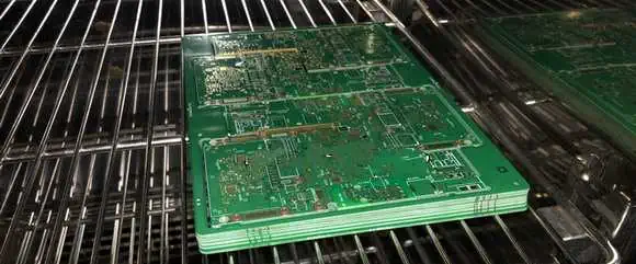
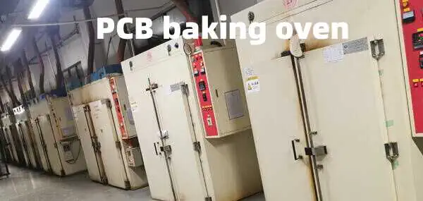
The progress in the PCB industry has led us to witness great inventions and upgrades in this domain. In this aspect, PCB baking is an important factor that demands our attention.
When we are learning about PCBs, we cannot forget the importance of PCB baking. So what is PCB baking? We are going to dig deeper into this concept for you today in this post. But before we get on with it, we need to know why PCBs are important.
Well, PCBs are significant for us because you cannot use your mobile phone or a home appliance without a PCB. They are also good for product miniaturization to optimize their functioning. However, with time the PCB producers faced some problems with the lamination and mounting. Therefore an applicable solution in the form of PCB baking was introduced.
Today, PCB baking is crucial for the protection against delamination on small and sensitive PCBs.
PCB baking is a special method that completely dries the PCBs. The purpose of this method is that there should be no moisture in the PCBs at all. Moisture can complicate the performance of PCBs because it causes corrosion and might also be a possible reason for electrical failures and short circuits. Therefore a preventative measure was important in the form of PCB baking to stop this moisture from damaging the circuit boards completely. Well, this is not it. How much your PCBs will absorb the moisture depends on their substrates. Some substrates are good at water resistance, while others are not. Speaking of PCB baking, you need to know that it is not a piece of cake.
There are some important considerations. But for this section, we are going to give you a quick overview of the process. You need to bake the PCBs in a reliable oven at an optimum temperature which is 130 degrees centigrade. This much heat is sufficient for the PCBs to have their moisture fully evaporated. As we have mentioned earlier, PCB baking is good for moisture evaporation to prevent delamination, but another good benefit of this method is that it also stops moisture outgassing. Outgassing mainly damages the circuit board panels and hampers the PCB performance.
Why do PCB Baking?
You must be thinking, do you really need to go for PCB baking? Well, yes, you have to! Because there is a possible chance a single trace of moisture can negatively impact your PCBs. Therefore, to make sure your PCBs are functioning normally, you need to bake them at a fixed temperature.
Also, when condensation interacts with the copper plates of the PCBs, it causes outgassing which is not good for the overall structure of the PCBs. It also damages the soldering, and the connection between the PCB parts and the boards becomes weak. One another impressive advantage of PCB baking is that it prevents chances of delamination as well.
Do we need PCB Baking?
Yes, experts believe that all types of PCBs must undergo baking. It is because whether your PCBs are simple and small or big and complex, PCB baking will just enhance their longevity and performance in the long run. Plus, it will exclude moisture and dry out the PCBs to protect them from the risk mentioned earlier.
Well, one thing to note about PCB baking is that there is no fixed time for it. Instead, PCB baking can be done at any point in the PCB production process. But the ultimate goal is to remove the moisture from the PCBs.
Fixing Conditions for PCB Baking
Well, by far, you know why we need to consider PCB baking. Also, you have a general overview of how it takes place. But in this section, we are going to see some conditions for PCB baking to drive good results from it.
These are industrial conditions, and almost every PCB producer sticks to these guidelines for making PCB baking an effortless process. Keep in mind that these are the conditions when you are using OSPsurface finish.
If the shelf life of PCB is up to 2 months, then it is crucial to fully bake it at 120 degrees centigrade for a straight hour.
In case a producer wants to store the PCBs for up to 12 months, then baking them at 120 degrees centigrade for two hours will prove to be beneficial.
In case a producer has stored the PCBs for 6-12 months after their production, then it is important that they bake their PCBs for four hours.
If the storage duration has exceeded 12 months, then it is better to bake them at 120 degrees centigrade for 6 hours. In these cases, experts don’t recommend such PCBs for usage because alterations and damage to the PCBs layers are more likely to occur. Therefore damaged layers hamper the performance of the PCBs. Besides, weak soldering and insatiability of the PCBs can also happen due to expired PCBs. Problems with the solder paste and chances of detachment of the PCB parts with the boards can also occur due to expired PCBs. The producers must change their options for surface finish and switch to ENIG in order to make PCBs able to last for 12 months easily. It will protect the PCB layers as well, plus the chances of contamination will be none.
After baking, the producer can keep the baked PCBs for a maximum of 5 days only and then immediately publish online or deliver them within five days. If there is a delay, it is important to rebake them before listing them online.
If your PCBs are large in size, then it is better to stack them in a flat alignment in which only 30 PCBs can be included in the batch. After this, we need to bake them and then put them on a flat surface to let them cool completely for ten to fifteen minutes. During this, keep an anti-bending tool with yourself so that you can immediately use it before things get complicated due to warping. Keep the PCBs horizontal so that the chances of warping will be less.
In case you are working on small to medium-sized PCBs, then it is important to stack them flat, and in this case, you can include 40 PCBs in a single badge. When our PCBs are small, we can arrange them in a vertical way easily. Just like the large PCBs, you also need to cool them for ten minutes. Use an anti-bending tool to prevent the risk of warping.
Now it’s time to quickly take a look at the precautions you need to consider while PCB baking. These will help you execute the process without any hustle in a safe and protected manner.
Precautions for PCB Baking
Make sure to maintain the temperature for PCB baking. Extra temperature for PCB baking can instead damage the PCBs during the process. Also, if you are unable to provide them with sufficient heat, the moisture will not be removed completely from the setup.
After baking, it is important to use the PCBs immediately. Due to some reasons, if it’s not possible, then it is better to rebake them or protect them from interacting with moisture by proper sealing.
It is beneficial to rely on a durable drying mechanism for PCB baking to provide the PCBs with sufficient heat to remove moisture.
Experts believe that always relying on fresh and high-quality PCBs for soldering will eventually pay off the PCB baking in the end as compared to using expired and substandard PCBs.
Try not to voltage industrial guidelines and quality standards when you are in the middle of the process so that you can completely make sure that your PCBs have been dried through baking.
Conclusion
Here you have all the important aspects of PCB baking. We have tried to discuss the industrial guidelines and expert opinions for the sake of your ease and seamless experience with PCB baking. It is important to know there are different factors that influence PCB baking.
Being a producer, you must be able to look out for these factors to avoid complications in PCB baking. Other than this, now you know what precautions are important when you want to go for PCB baking.
All in all, PCB baking is a crucial process that helps you improve the performance of your PCBs on all counts so that they can serve your clients longer through consistent and flawless functioning.
Chokes, which are also referred to as inductors, are useful in blocking higher frequencies when passing lower frequencies and direct current of an alternating current in any electrical circuit. This name results from choking or blocking high frequencies when passing the low frequencies.
Also, the choke is made up of an insulated wire coil that is usually wound on the magnetic core, though some are made up of a bead (donut-shaped) of a ferrite material that is strung on the wire.
What are Electronic Chokes?
Chokes can be described as one of the three main passive components utilized in any electronic circuit. The remaining two passive components that are usually used with inductors are the resistors and capacitors. Inductors are known to have a simple form as well as materials which they are manufactured from, however they could perform different functions within the electronic circuits.
Furthermore, the inductors help in storing electrical energy inside the magnetic field as well as resist any sudden current change that allows their utilization in applications like EMI filtering, analog circuits, power supplies (switch mode), RF circuits, signal processing and analog circuits.
Typically manufactured from wire that is wrapped around a magnetic core of iron or ferrite, inductors could be drum core, rod core, toroid form, etc. These inductors are usually calculated in henries (nanohenries, microhenries, and millihenries, which help in the measurement of the overall magnetic field strength. This is why the more the wire windings are placed round the core, the greater its inductance.
Chokes come in two major types: automatic or electrical and manual. For example, in motorcycles, the manual chokes usually have a button or lever that a rider could use in adjusting the choke to suit the need. Whenever this level gets pulled or you press the button, this choke becomes engaged and the air flow in the carburetor becomes restricted.
Also, the automatic chokes are usually more convenient for riders because it doesn’t need any manual adjustment. Automatic chokes are typically made up of thermostatic springs which are connected to the carburetor’s valve. Its spring would be calibrated so as to open as well as close the valve with respect to the engine’s temperature.
Chokes function through the provision of high inductance paths in the circuit that limits the quantity of current that flows via the circuit through the introduction of a “back EMF” which opposes the current change. Speaking simply, this choke serves as the inductor which helps in storing energy inside a magnetic field whenever there is a flow of current through it.
This energy stored inside the magnetic field also opposes the current flow change via the choke. Whenever the flow of current via the choke increases, this inductor helps in resisting the change through the generation of a back electromotive force (EMF) in the current flow’s opposite direction. The back EMF serves as a current flow barrier and helps in reducing the current that flows via the circuit.
Asides limiting its current, you can also use a choke in filtering unwanted ripple and electrical noise from a circuit’s output. The high inductance values of a choke let it serve as low-pass filters that could take out high-frequency noise out of an output signal.
You can use chokes in audio circuits and power supplies to help in reducing noise as well as improving the quality of the signal. Also, it is utilized in circuits of high frequency to help suppress any unwanted RFI (radio frequency interference), which could have an effect on how different electronic devices perform.
How Electronic Choke Circuit Diagram are Wired
Electronic devices, which are also called automatic choke, are wired in a combustion engine’s carburetor. This electric choke is usually controlled by the electronic control modules of the engine, and is utilized in order to regulate the quantity of fuel and air that enters the engine when the starting process is on.
An electronic choke’s wiring typically deals with the connection of the choke into the carburetor, and then connecting it into the battery and then to the ECM. An electric choke’s specific wiring would depend upon the model and make of the carburetor and engine.
Below is an overview if the entire process of wiring
Connect your electronic choke circuit diagram into the carburetor
This electronic choke is usually mounted on top of the carburetor and then is connected onto the air intake of the carburetor. The connection is created making use of the choke rod or choke tube, which connects an electric choke into the air intake of the carburetor.
Connection of the electronic choke onto the battery
You power this electric choke by the battery of the vehicle. Therefore a negative and positive wire has to be connected into the electric choke. Typically, this positive wire is connected to the battery’s positive terminal, while the negative wire would be connected into the negative terminal of the battery to the ground of the engine.
Connection of the electronic choke into the ECM
The control of the electric choke happens with the help of the ECM of the engine. The ECM’s wire is attached onto the electric choke so as to control the choke’s closing and opening.
In addition, noting the variation in the electronic choke wiring is important. This variation is dependent on the carburetor and engine type, and is usually recommended that you work with the instructions of the manufacturers or the service manual of the vehicle for any wiring instruction.
How the Electronic Choke Circuit Diagram Functions in the Power Supply
For power supply, the choke serves as an inductor used in filtering the power supply’s DC output. The choke functions through resisting current changes that flow through it. This helps in the smoothening out of all DC output voltage variations.
Particularly, this is very useful for any power supply used in supplying power to the electronic circuits, because it helps in reducing ripple and noise in a DC output that could cause issues for electronic components that are sensitive.
Power supply chokes functions by offering high inductive reactance to an input current’s AC component, while having a low DC resistance. With this, the current’s AC component would be blocked when this DC component is made to pass through. Also, this choke aids in the suppression of high-frequency noise, which might be present in any input power. It is important in ripple and noise sensitive electronic circuits, like those utilized in video and audio equipment.
Why Your Electric Choke Circuit Diagram Might Not Work
Your unit may not work as a result of two major reasons. This electronic choke circuit diagram may have been malfunctioned, or another problem may be affecting the power supply. You may test the power, if you have a multimeter. You can achieve this through the detachment of the choke and then getting meter leads coming in contact with the wires of the electric choke while running fast tucks over.
When everything works fine, then the wire would have a reading of about 12 to 14 volts AC. You can find it on the majority of electrical scooter displays. When performing the test, you must note that chokes usually run off a lightning circuit, which is most times AC on scooters. So, make sure you conduct a test with a meter to help in setting the DC and AC.
This electric choke functions at DC or AC so far you have a reading that falls within 12 to 14 volts. Another tip for maintenance is that you should understand how to check the quantity of oil present in the kick electric scooter.
What are the Applications of the Electrical Choke Coils?
Electrical choke coils are useful for the filtration output of the rectifier as well as offer a DC output that is pure.
Due to its great magnetic property, you can use them in circuit breakers, relays etc.
You can utilize them in devices used in different radio stations
Used in any resonance circuits
Useful for a signal transmission system
Why is Choke Coil Utilized in the Fluorescent Tube Lights?
You can connect the choke coil in series using a tube light. This limits the starting time current during the bimetallic contact’s closed condition inside the starter.
The high voltage is very important for getting ionized gas in a tube light. This choke helps in the creation of high voltages passing across it as well as aids in gas ionization.
Conclusion
The significance of electronic choke circuit diagrams can never be overemphasized. Chokes can be described as one of the three main passive components utilized in any electronic circuit. The remaining two passive components that are usually used with inductors are the resistors and capacitors. Chokes are inductors that are useful in blocking higher frequency when passing lower frequencies and direct current of an alternating current in any electrical circuit. Your unit may not work as a result of two major reasons. This electronic choke circuit diagram may have been malfunctioned, or another problem may be affecting the power supply.
The designs of electronics are important if we are aiming for industrial-grade consumer electronics. Therefore, for this reason, you need to rely on an efficient electronic design service/company for your own good. There have been cases when buyers faced different problems regarding electronic designs due to bad choices of services.
There is no doubt that if you hire a reliable electronic design service/company, you will be able to procure different benefits in the long run. The production of electronics, prototyping, assembling, and maintenance becomes easier with accurate designs.
The role of an electronic design service/company proves to be crucial here since it can help producers meet the market trends and the latest electronic designs as well.
What is an Electronic Design Company?
The sole purpose of an electronic design service/company is to leverage new technologies to develop the latest designs for consumer and industrial electronics. The electronic designs are critical because they have a seamless path for bulk electronics production and efficient and fast prototyping for the electronics as well.
An electronic design service/company relies on designing software for this purpose so that the design completion and testing can be done in an effortless way on all counts. A brand like this is able to communicate professionally with its clients to develop desired designs for electronics. These companies are able to develop designs of electronics that are used in technical domains like robotics, artificial intelligence, and automotive industries.
You might be thinking, why do you need to hire or consider an electronic design service/ company? Well, there can be many reasons for it. However, not every situation is the same for every customer. Some people want to rely on personal and customized electronic designs instead of hiring a company for them.
Experts believe that you need to see what you are looking for. After you have determined this, you can choose from both options easily. But hiring an electronic design service/company can help you with your problems in different ways. Let’s see them below:
If you don’t have many resources, you can consult a company like this.
In case your designs require rare and less accessible resources and materials, only an electronic design service/company can help you with this
You might not be able to tackle risks and concerns that might occur during the process.
You also might not have the proper knowledge and experience to handle electronic design development, which can complicate the process for you.
Top Electronic Design Companies
1. Green Circuits, USA.
Your first option to explore must be Green Circuits, USA. It is because they are one of the most appreciated and cherished electronic design developers in the region. They know all about the nitty-gritty of this field, so their experts can help you with your design requirements on all counts. Not just design development, they can easily provide you with other services like prototyping, production, and after-services like maintenance as well. Their designs prove to be handy for fields like healthcare, the automotive industry, and many others.
2. Integra Sources, Kazakhstan.
Next, we have Integra Sources, Kazakhstan. They are experts in design development by relying on the latest and highly advanced design software for this purpose. They have recruited highly skilled professionals in this regard. From turnkey designs to simple ones, they can do it all for you. You can easily rely on their designs if you are coming from the domains like IoTs, education, healthcare, media/entertainment, and automation. The customers of Integra Sources also get after-market services to ensure you are not having trouble with your electronics and designs. Plus, their associates will reach out as soon as possible to address your queries in time.
3. eInfochips, USA, India.
Another good contender on this list is eInfochips, and currently, they are operating in the USA and India. They have been the most established electronic design service/company in these regions that are providing their customers with different types of electronic designs and engineering services. You can explore them based on their huge range of products listed on their website. From healthcare to the automotive industries, they have been successful in productive collaborations.
1. Corintech, UK.
The multitude of Cointech is not much impressive as compared to other companies, but still, we cannot further continue without mentioning their role as an electronic design service/company here. They have been able to form strong working relationships with their partners over the years through the successful delivery of electronic designs and providing other services. Their prototype is also useful for the development of electronics. They have contributed to the market by relying on their products and have also reeled in great sales in the last couple of years as well.
5. Newmatik, Germany, Romania.
Newmatic is functional in Germany and Romania. It is a branch of ESO electronics. Basically, ESO is a contract electronics manufacturer that has been functional for many years. However, the company operates in Germany at its core. They are offering services like prototyping, development of PCBs, electronic design development, and also PCBS production, which is a piece of cake. They have a stellar portfolio, and their website houses different products offered by them. You can further check them out through their website, where they have mentioned all about them for your convenience.
6. Softeq
We are going to discuss Softeq, which is functioning in different regions of the world, including Lithuania, Belarus, the UK, Germany, and the USA. They are experts in full-stack development, which means you can hire them for your software and hardware needs both. Being an electronic design service/company, their designs are applicable to different electronics used in multiple domains. They are solely into software and design development which makes it easier to hire them for their clients.
7. Sierra Circuits
Sierra Circuits, which is operational in the USA, is a contributor to Silicon Valley. The services offered by them include quick-turn PCB development and medium production. Besides, you can also avail benefits from their impeccable electronic designs. Different industries are relying on the designs offered by Sierra Circuits today.
8. Axonim
The next one is Axonim which has no parallel being an electronic design service/company in Lithuania. It is a full-range software and electronic design development company. Besides, you can hire them for optical device production, automated systems, and manufacturing drone equipment, including hardware and software for operating drones. Their products and services are also reliable for the sustenance of different fields like oil and gas and telecommunication. They have a huge partner base that they have successfully contributed over the years.
9. Inelmatic Electronics
Inelmatic Electronics is a Chinese electronic design service/company. Their products and services are reliable for clients coming from the automotive, transportation, healthcare, and defense industries. They are also collaborating with established European companies to offer their services. They are experts in turnkey solutions and also offer flawless electronic designs to their clients. Their expertise further includes HMIs, touchscreen development, optical device production, and the development of the latest type of displays for electronics.
10. AVL
We now have AVL, which is an Austrian electronic design service/company. You can avail of their services in terms of prototyping and design development for electronics. Their solutions for reducing carbon dioxide production are not only viable but also effective for application. The field of aviation and construction are both relying on AVL for their expertise and remarkable products.
11. Mako Design
They are also a good option to look for in terms of electronic design development. They are supporting and collaborating with budding marketers and small-range companies to offer their services. You can even rely on their product engineering services to bring your ideas into reality. Another good thing about this company is that they always rely on the latest software and tech to improve their designs and services for the customers.
12. Consonance
Consonance is a Polish company that is contributing to the progress of multiple fields through its services and products. They can be your number one medical equipment developer, and you can rely on their industrial-grade medical components for the improvement of medical equipment used in hospitals and clinics. They are also good with prototypes, so if you are looking for a multipurpose company, then Consonance can help you in this regard.
13. Voler Systems
Voler Systems have attracted different clients and customers over the years by providing them with exceptional services and products. They are reliable in terms of electronics engineering so that you can bring your ideas regarding IoTs, and medical equipment development to reality. Their workers rely on the latest and tech-based sensors and wireless interfaces to give an edge to their products for their customers. Analog and catalog designing is also an area of expertise of Voler Systems. If you are looking for manufacturing preparation services, Filed programmable gate array development, then this company can be a good option for you.
Many people out there feel dubious if they should hire an electronic design service/company or not. Sometimes you get stuck with such problems with the design development that only a professional service can provide you with its solution. So below, we will see how these companies can benefit you:
You can have your products manufactured and delivered in no time.
You can ensure flawless and industrial-grade quality electronic designs.
No matter where you are located, you can have your products delivered to your doorstep.
These companies rely on the latest tech equipment that you personally cannot afford on your own
Advanced design software used by these companies provides you with exceptional electronic designs.
Sometimes you need to give an edge to your designs, and for this, you can hire an electronic design service/company for other services as well.
Factors to Ponder while Choosing an Electronic Design Company
There is no doubt that some factors greatly help you with choosing a good and reliable electronic design service/company. So that you can save yourself from scammers and low-quality products plus, you can even save time with cheap services by completely evaluating your options.
· History & reputation
The first thing you need to look for is the service history and reputation. There are different ways that you can do it. You can even look up the internet to research your options. Plus, make sure to investigate more about these companies through expert opinions, and if you can, you can even meet these experts to have their honest review of your options.
· Collaborative approach
The next factor that helps you rely on a good electronic design service/company is the collaborative approach. Are they available for you 24/7? Are they taking you and your requirements seriously? Can they meet your deadlines and provide quality products and services in emergency situations? How much of a collaborative approach they are aiming for matters a lot that sets a bad and a good electronic design service/company for you.
· Communication
The third factor that you must pay attention to is communication and project management. Communication is all that you want to look for in an electronic design service/company. So that you can see if they are able to tackle your ideas and meet your requirements or not. Plus, how they can handle emergency situations through balanced professional client communication is also a distinguishing factor. Other than this, the project management of a company also shows how much they are into professionalism. There is no doubt that there are some companies that cannot handle the pressure and mess the projects up. Therefore if you are a buyer who always throws bulk projects to the company, then make sure to check them first or at least inquire about this from them to avoid future complications.
· Payment
The last thing is the payment and service charges. For this, you can discuss their service charges and fee individually. How much you are going to pay depends on your requirements and needs. Some companies charge you differently for the same service. Therefore, in this case, you must go for the affordable option. But in case you have some expensive demands, then it is obvious that you would have to invest a big chunk of money in the company as well.
Wrap Up!
RayPCB hopes that now you can easily choose from the above-mentioned companies to fulfill your electronic design development needs. The best part about these companies is that they are multirange, meaning you can hire them for other services as well other than electronic design development. A good electronic design service/company is one that does not abandon you at every step and unconditionally meets your requirements, and helps you with your ideas on all counts. Therefore, we have explained some of the contributing factors that can help you with choosing the right choice of company for yourself.
Though there are lots of circuit diagrams out there, integral circuit diagrams are usually represented using symbols such as triangles, rectangles, and more. These circuit connections are conveniently placed all over the rectangle without any regard for the pins’ physical positioning. In the digital world of today, integrated circuits form the brain and heart of the majority of circuits.
The integrated circuit diagram is important. In each electronics project that you create, you will most probably find at least one integrated circuit. Therefore it is important that you have a deep understanding of them. With an integrated circuit diagram, you will have a detailed understanding of the way they work as well as their applications.
Continue reading this article to understanding ways for creating the integrated circuit diagram with free design features and templates
What Do Integrated Circuits Mean?
Majority of today’s entertainment tools, equipment, and gadgets integrate the integrated circuits which perform some functions, which makes users enjoy a fascinating experience. From the toddlers’ toys to complex game studios present in the casinos, the hardware serves as the main component of our entertainment technology.
In addition, the integrated circuits can be described as circuits which could have many transistors as well as other circuit elements that are present on one die (this is a silicon piece which contains output and input devices and active devices. They are composed of some special materials referred to as semiconductors with gallium arsenide and silicon as the most common.
Also, its evolution is a huge milestone when talking about the history of today’s industry as it resulted in a revolution in the capability of computation as a result of the long trend in the density gains, performance, as well as cost with scaling. Fortunately, these circuits can be created making use of different technologies.
However, overtime, the CMOS technology is now the most prevalent and industry de-facto method chosen in the industry. Its main benefits over the remaining technologies include its easy integration of the circuit components as well as the low static consumption of power. This is the major technology utilized in the manufacturing of microcontrollers, analog-to-digital converters, microprocessors FPGAs (this is the integrated circuit which has different identical cells as well as programmable interconnections), and others utilized during the development of the entertainment hardware.
Also, its continual improvement has led to a reduction in the dame gadgets size, better performance, better battery management for devices that are battery-operated, cost and the hardware ergonomics.
An integrated circuit diagram has to do with the operational amplifier, envelope detector, rheostat, capacitor, differential, amplifier, and other components. There are integrated circuits having at least two independent circuits, which share a power supply. IC features a complex layer of copper, semiconductor wagers, as well as other materials, which interconnects to create resistors, transistor, and other components inside a circuit.
Envelope detectors can be described as the one of the most important components of the inputs. This detector takes high-frequency signals as an input and then offers an output, which is the envelope of the original signal.
Op-amps
Op-amps work well for the amplification of direct current. Most times, they are utilized in filtering, signal conditioning, as well as other mathematical operations. In addition, it is a very important single device used in the analog electronic circuitries.
Differential amplifier
Amplifiers utilized in an integrated circuit diagram are of two types. These are differential amplifiers and operational amplifiers. Differential amplifiers help in the amplification of the difference in-between both input signals.
What are the Important Tips to look into during the Creation of the Integrated Circuit Diagram?
Creating an integrated circuit diagram should be easy if you have a deep and thorough understanding of the steps involved. Furthermore, there are some connections you must correct so as to prevent any possible breakage inside the circuit. You can consider the following tips during the integrated circuit diagram creation.
You should feed the RF input at the circuit or system’s input
The resistors’ value utilized inside the circuit has to be thoroughly marked
You must mark the diodes’ negative and positive sides
The connections gotten from the diodes’ negative and positive sides must be marked rightly inside your integrated circuit diagram
Tools for Integrated Circuit Diagram Creation
The creation of the integrated circuit diagram needs specially designed tools that can handle this work’s unique requirements. There are different software packages that offer the required tools for creating detailed and accurate integrated circuit diagrams. Let’s consider them
EDA Software
EDA (Electronic Design Automation) Software is designed specifically for the creation of a n integrated circuit diagram. The software offers different tools which permit a designer to crate, stimulate, as well as test an integrated circuit. The EDA software is usually utilized by expert designers that need to create their complex circuits with many components and layers.
CAD (Computer-Aided Design) Software
The CAD software is another alternative for creating the integrated circuit diagram. The software is more of a general purpose compared to the EDA software. Also, they are utilized in different design tasks, which include engineering, architecture, product design, and design tasks. The CAD software offers different tools for the creation and editing of the diagrams, which includes their ability to create the 3D models.
Creating the Integrated Circuit Diagram with EdrawMax Online
Creating your integrated circuit diagram with EdrawMax online is easy. You can import icons or images from your systems, DropBox, or Google Drive in the electrical circuit makers. Extra media content would be needed for electrical circuit diagrams, which makes it much more creative.
Log into EdrawMax Online
Register with your email address and then to log in to the EdrawMax Online, if this is your first time utilizing the tool, you may create an account that is personalized making use of your professional or personal email address.
Select a Template
Different free diagram templates are usually added using EdrawMax Online. Using the search section, type in the keyword to locate your pre-designed template. You may also explore several diagram sets. For cases like this, you can find different electrical circuit diagrams under the “Engineering” and “Electrical Engineering” sections.
Different diagram sets are available as well. These include Circuits and Logic, Basic Electrical, Systems Diagrams, and Industrial Control System. Alternatively, you may create any diagram of choice just by clicking the “+” present in the software’s online canvas.
Do some work on research
Integrated circuits are usually represented in electronic schematic diagrams as rectangles having circuit connections that are placed conveniently around the rectangle and without any regard for the pins’ physical positioning.
Customize your Diagram
Change the integrated circuit diagram’s color or add some relevant data. With respect to your research, you may remove or add electrical content or symbols. Due to the fact that it is related to electrical engineering research, you may include additional relevant data regarding different circuit diagrams.
Export it and Share it
After completing the required diagram, exporting it and sharing it with clients or colleagues becomes easy. The diagram can also be exported into different formats. These include JPEG, Graphics, HTML, and PDF. Also, the designs can be shared on different social media platforms. Putting this simply, your integrated circuit diagram can be exported to those files you want within seconds.
This integrated circuit diagram serves as a circuit design’s visual representation. It reveals the connection present between the different components as well as the circuit’s layout present on the chip. Engineers use this diagram to make sure that a circuit would function effectively and that it will be efficiently manufactured.
The integrated circuit diagram is an important part of electronic circuits design. The diagrams are utilized in communicating the circuit components’ layers to the producer, who will then create your physical circuit. Also, the integrated circuit diagram comes with many applications.
The importance of the integrated circuit diagram cannot be overemphasized. First, they permit engineers to be able to visualize their circuit design as well as identify any potential issues before manufacturing the circuit. This will save you money and time by avoiding any costly errors during the manufacturing process.
In addition, the integrated circuit diagram is useful in documenting the design to serve future purposes. This is necessary to maintain the product’s reliability and quality over time. Also, this drawing also serves as reference for changes that are made to your design and can be utilized for troubleshooting any issues that may arise in the near future.
Conclusion
For integrated circuits, lots of electronic components will be interconnected on one semiconductor material chip. We hope that the circuit diagram would allow you to have a thorough understanding of its functionality.
Generally, the integrated circuit diagram plays an important role in the designing, developing, manufacturing, as well as maintenance of the electronic circuits. Also, they offer an important visual representation of a circuit layout as well as facilitate string communication between the manufacturers and the designers.
Electronic or electrical amplifiers can be described as circuits which make use of external power supply or generating output signals which are a bigger replica of the input.
Audio amplifiers, which can be described as a recognizable application, are useful for increasing a speaker’s volume to allow the sound to be heard easily in any large area. Though voltage can be described as the most common of all amplified input signals, these amplifiers may also be designed so as to increase the current. Any amplifier which increases the current drive of an output is referred to as the power amplifier.
Majority of amplifiers perform linear amplification. However, some are naturally logarithmic. In circuit diagrams, amplifiers are represented with a triangle. First, let us consider what an amplifier circuit diagram means as well as its types.
Amplifier circuit diagrams are made up of one signal pick-up transducer, which is followed by any small signal amplifier, output transducer, as well as one large signal amplifier. Initially, the amplifier circuit diagram comes in two types i.e. power amplifier circuits and voltage amplifier circuits.
Voltage amplifier circuit
The main function of this type of amplifier circuit diagram is to help in raising the signal’s voltage level. It is specially designed for achieving the largest gain possible. You can draw extremely little power out of the output. In order to achieve any high amplification of voltage, then the requirements below has to be met by your voltage amplifier circuits.
The transducer features a thin base i.e. beta/high transistors (higher than 100) is utilized.
Fairly low impedance compared to the output impedance.
The voltage amplifier will always function at a low current of around 1mA, in order to allow high collector loads that are required for a high gain in voltage.
Most of the time, the R-C couple is necessary for coupling the different voltage amplifier circuit stages due to the fact that it is cheaper when it comes to portability and cost.
Power amplifier circuit
The main function of this type of amplifier circuit diagram is to raise the input signal’s power level. In order to get a large power for the output, then there must be a large input-signal voltage. This is why for electronic systems, voltage amplifier circuits usually precedes the power amplifier circuits. Also, this is the reason behind power amplifier circuits called the large-signal amplifier circuits.
The regions found behind power amplifier circuits is referred to as large-signal amplifier circuits because it has the ability to draw power out of the DC source, which is connected in the output and then converts it in an appropriate AC signal or sine wave. Power amplification cannot occur here because it doesn’t work in line with the physics’ rule. In order to achieve greater power amplification, then the circuit has to work with the requirements below
For power amplification, there is heat produced in a transistor during an operation, to ensure large-sized power transistors are used
Collector resistance is made low
Transistors with thick bases not voltage amplifier (beta/smaller) is useful in handling large currents
Most times the transformer-couple is useful in impedance matching.
What are the Important Features of Amplifier Circuits?
An amplifier’s quality may be measured through some specifications referred to as the figures of merit. Let’s consider them
Noise: This refers to the additional information that is unwanted, but included inside the output
Bandwidth: This is the range of frequency where the amplifier will be able to function
Skew rate: This is highest rate of output change
Linearity: degree of proportionality found in-between the output and input signals
Gain: This is the most significant. It is the ratio between the output and input signals magnitudes
Stability: Ability to provide reliable and constant output.
Output dynamic range: This describes the ratio between the smallest and largest useful levels of output
Aside from the main or basic types, amplifiers come in several types. This is grouped by their characteristics, application or operation. Some of them include
Power Amplifiers
Though not a type from the technical point of view, the power amplifiers form a general term which has to do with the quantity of power provided by your power supply circuits as well as the power that is delivered onto the load. This is usually utilized in a circuit’s final output stages.
Some examples are push-pull amplifiers, servo motor amplifiers, audio power amplifiers, as well as the RF power amplifier. Once again, we will be considering how power amplifiers are classified, because they play a very significant role.
Operational Amplifiers
This is another important type, also known as op-amps. This is an IC which functions as voltage amplifiers. It also has a differential input. Furthermore, it features a negative and positive input, as well as one output with extremely high gain. Initially, the creation of op-amps was done using valves.
Transistor Amplifiers
This is a popular type of amplifier that is especially designed for engineering students. It is a well-known amplifier. It is a high output multi-configuration amplifier which makes use of transistors as its working base.
Vacuum (or) Valve tube amplifiers
This type of amplifier makes use of vacuum tubes for providing increased voltage or power output. As mentioned earlier, op-amps were initially the valve type; however, the ICs replaced them as soon as they became less expensive, at least, in the smaller applications. However, for high-power applications, they are still useful due to their output quality and cost effectiveness. Also, they are useful in military, radar, high power UHF and radio transmitter applications.
Klystron
This is a special linear vacuum tube utilized as amplifiers in the high-radio frequencies. Also, it is very precise and is useful in large-scale operations, and usually categorized microwave amplifiers.
Distributed Amplifiers
These are amplifiers, which makes use of transmission lines for splitting the input temporarily as well as amplifying each segment. You can find them in oscilloscopes.
Instrument Amplifiers
These amplifiers are specially designed for amplifying music, voice, or sound. It is mainly used in applications for musical instruments.
Different Circuit Currents
Let’s consider the different circuit currents present in a full amplifier circuit board diagram.
Base Current
Whenever there is no applied signal on a base circuit, the DC base current will flow as a result of the biasing current. Whenever the AC signal has been removed, the AC base current will also flow.
Emitter current
The DC emitter current will flow whenever there is no signal applied.
Collector current
Whenever there is no signal applied, the DC collector IC will flow because of the biasing current. Whenever an AC signal has been applied, then the AC collector current flows as well.
The practical circuit of the transistor amplifier represents a specific voltage divider biasing circuit. The different prominent elements of a circuit as well as their function can be described below.
The capacitor helps in the coupling of an input signal to the transistor’s base. Input capacitor permits an AC signal, but helps in isolating a source of signal. When the capacitor isn’t present, then the input signal will become applied directly, thereby changing the bias.
Biasing Circuit
Resistors RE, R2, and R1 form the stabilization and biasing circuit. This aids in establishing the right point of operation.
You can employ the capacitor in the parallel form into your emitter resistor. Thee
Coupling Capacitor
This capacitor is usually seen at the final periods of one stage and then connects it onto the second stage. Because it helps in the coupling of two stages, you can call it a coupling capacitor. The capacitor will block the DC of one of the stages and make it enter the second but permits the passing of the AC. This is why it is referred to as the blocking capacitor.
Because of the coupling capacitor, the output that forms across the resistor is completely free from the DC voltage of the collector. When you don’t find this, the next phase’ bias conditions would be changed drastically as a result of the RC’s shunting effect because it would come in a parallel form to the following stage.
Load Resistor
The resistance that is connected at its output is referred to as the load resistor. Whenever a number of phases are utilized, then the RL represents the next stage’s input resistance.
Conclusion
By now, you should understand what the amplifier circuit board diagram is and how it works. Almost all the electronic equipment out there has to include some amplifying means for the signals. The application of the amplifier circuit board diagram can be seen in scientific equipment, medical devices, military tools, automation, communication devices, as well as household equipment. Aside from the main or basic types, amplifiers come in several types. This is grouped by their characteristics, application or operation.