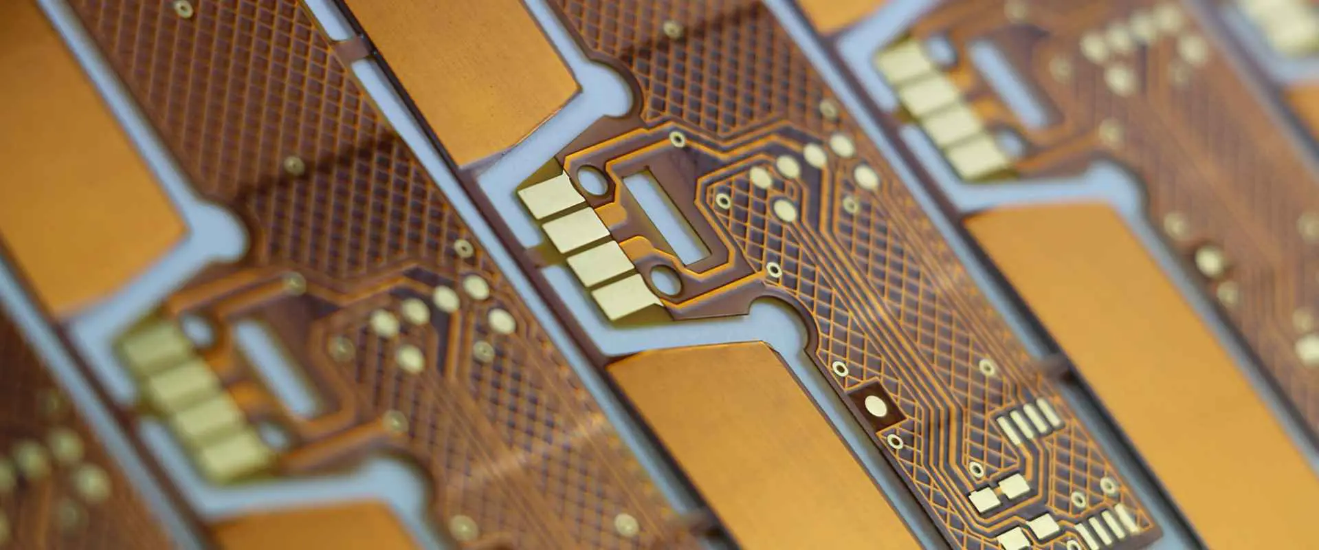
The IPC 4203B-2018 standard represents a critical specification in the flexible printed circuit board (flex PCB) industry, establishing comprehensive requirements for cover and bonding materials used in flexible electronic assemblies. As electronic devices continue to evolve toward more compact, lightweight, and flexible form factors, the importance of standardized materials and processes becomes paramount to ensuring reliability, manufacturability, and performance consistency across the industry.
Powered By EmbedPress
Background and Development
The Institute for Printed Circuits (IPC), now known as the Association Connecting Electronics Industries, developed IPC 4203B-2018 as an evolution of previous standards addressing the growing complexity and demanding applications of flexible circuits. This standard emerged from the need to address technological advances in materials science, manufacturing processes, and application requirements that were not adequately covered by earlier specifications.
Flexible printed circuits have become increasingly prevalent in applications ranging from consumer electronics and automotive systems to aerospace and medical devices. The unique mechanical properties required for these applications—including the ability to bend, fold, and flex repeatedly without failure—necessitate specialized materials and rigorous testing protocols that differ significantly from those used in rigid PCB applications.
Scope and Application
IPC 4203B-2018 specifically addresses coverlay materials and adhesive systems used in the construction of flexible printed circuits. Coverlay serves as a protective layer that provides electrical insulation, environmental protection, and mechanical support to the underlying circuitry. The standard encompasses both adhesive-based coverlays and adhesiveless systems, recognizing the diverse manufacturing approaches employed across the industry.
The standard applies to single-sided and double-sided flexible circuits, as well as multi-layer flexible assemblies. It covers materials used in various application environments, from benign indoor conditions to harsh industrial and automotive environments where temperature extremes, chemical exposure, and mechanical stress are significant factors.
Material Classifications and Requirements
One of the fundamental aspects of IPC 4203B-2018 is its systematic classification of cover and bonding materials based on their thermal, mechanical, and electrical properties. The standard establishes multiple categories that allow designers and manufacturers to select appropriate materials based on specific application requirements.
Thermal performance classifications address the maximum operating temperatures that materials can withstand while maintaining their protective and mechanical properties. These classifications are particularly critical in applications such as automotive under-hood electronics or industrial control systems where elevated temperatures are routine operating conditions.
The mechanical property requirements encompass tensile strength, elongation characteristics, tear resistance, and dimensional stability. These properties are essential for applications involving repeated flexing, such as hinges in laptops, connections in automotive doors, or wearable electronic devices. The standard specifies test methods and acceptance criteria that ensure materials can withstand the mechanical stresses encountered in their intended applications.
Electrical property specifications include dielectric strength, surface resistivity, and dielectric constant values. These parameters are crucial for maintaining signal integrity and preventing electrical failures in high-frequency applications or densely packed circuit configurations.
Adhesive Systems and Bonding Requirements
The standard provides detailed specifications for adhesive systems used to bond coverlay materials to flexible circuit substrates. These specifications address both structural adhesives used for permanent bonds and removable systems designed for applications requiring access to underlying circuitry for repair or modification.
Adhesive performance requirements include shear strength, peel strength, and thermal cycling resistance. The standard recognizes that adhesive performance can be significantly affected by surface preparation, application conditions, and curing parameters, providing guidance on process control measures necessary to achieve consistent results.
Environmental resistance requirements for adhesive systems address exposure to humidity, temperature cycling, chemical exposure, and UV radiation. These specifications ensure that bonded assemblies maintain their integrity throughout their intended service life, even when exposed to challenging environmental conditions.
Testing Methodologies and Quality Assurance
IPC 4203B-2018 establishes comprehensive testing protocols that enable manufacturers to verify material compliance and end-users to qualify materials for specific applications. The standard references numerous ASTM, IEC, and other IPC test methods while also defining specific procedures tailored to flexible circuit applications.
Mechanical testing procedures include bend radius testing, which determines the minimum radius to which a flexible circuit can be bent without damaging the coverlay or underlying circuitry. This testing is particularly important for applications involving repeated flexing, as it helps predict service life and reliability.
Thermal testing encompasses both steady-state temperature exposure and thermal cycling tests. These procedures evaluate material stability, dimensional changes, and property retention under various thermal conditions. The standard specifies conditioning periods, temperature profiles, and measurement techniques that ensure reproducible and meaningful results.
Electrical testing procedures address insulation resistance, dielectric strength, and surface resistivity measurements. These tests are performed both on virgin materials and after various environmental exposures to verify that electrical properties remain within acceptable limits throughout the material’s service life.
Manufacturing Process Considerations
The standard acknowledges that material performance is intimately linked to manufacturing processes and provides guidance on process parameters that affect final product quality. Lamination temperature and pressure profiles, adhesive application methods, and surface preparation requirements are addressed to help manufacturers achieve consistent results.
Process control recommendations include statistical process control methods, inspection criteria, and documentation requirements. These elements are essential for maintaining quality in production environments and for troubleshooting when quality issues arise.
The standard also addresses handling and storage requirements for cover and bonding materials, recognizing that improper handling can significantly affect material performance. Shelf life specifications, storage environmental conditions, and handling procedures help ensure that materials maintain their specified properties from receipt through final application.
Industry Impact and Adoption
Since its publication, IPC 4203B-2018 has become widely adopted across the flexible circuit industry, providing a common framework for material specification, qualification, and procurement. The standard has facilitated improved communication between material suppliers, circuit manufacturers, and end-users by establishing common terminology and test methods.
The standardization has also contributed to improved product reliability by ensuring that materials used in flexible circuits meet minimum performance requirements appropriate for their intended applications. This has been particularly beneficial in high-reliability applications such as aerospace and medical devices, where material failures can have significant consequences.
Future Considerations and Evolution
As technology continues to advance, the requirements placed on flexible circuit materials continue to evolve. Emerging applications such as foldable displays, wearable sensors, and Internet of Things devices present new challenges that may require updates to existing standards or development of new specifications.
The increasing emphasis on environmental sustainability is also influencing material selection and specification requirements. Future revisions of the standard may need to address recycling considerations, bio-based materials, and reduced environmental impact manufacturing processes.
Additionally, the trend toward higher frequency electronic applications is placing new demands on the electrical performance of coverlay materials, particularly in terms of signal integrity and electromagnetic interference considerations. These evolving requirements will likely drive future updates to the standard.
Conclusion
IPC 4203B-2018 represents a comprehensive and mature standard that addresses the critical requirements for cover and bonding materials in flexible printed circuits. By providing detailed specifications, test methods, and process guidance, the standard enables the reliable manufacture of flexible circuits for a wide range of applications. Its adoption has contributed significantly to improved product quality, enhanced reliability, and more efficient communication throughout the supply chain. As the flexible electronics industry continues to evolve, this standard will undoubtedly continue to serve as a foundational reference while adapting to meet emerging technological challenges and requirements.
The electronics manufacturing industry relies heavily on standardized processes to ensure consistent quality, reliability, and performance across printed circuit boards (PCBs). Among the various surface finishes available for PCB manufacturing, immersion silver has emerged as a popular choice due to its excellent electrical properties, cost-effectiveness, and environmental compliance. The IPC-4553A standard serves as the definitive guide for implementing immersion silver plating processes, providing manufacturers with comprehensive requirements and guidelines for achieving optimal results.
Powered By EmbedPress
Introduction to IPC-4553A
IPC-4553A, titled “Specification for Immersion Silver Plating for Printed Circuit Boards,” is a technical standard developed by the IPC (Association Connecting Electronics Industries) that establishes the requirements for immersion silver surface finishes on printed circuit boards. This standard replaced earlier versions and represents the current industry benchmark for immersion silver plating processes. The specification covers everything from chemical composition and process parameters to quality control measures and testing procedures.
The development of IPC-4553A arose from the need to standardize what had become an increasingly popular surface finish option in the electronics industry. As environmental regulations tightened and manufacturers sought alternatives to lead-containing finishes, immersion silver emerged as an attractive solution that offered excellent solderability while maintaining compliance with RoHS (Restriction of Hazardous Substances) directives.
The Science Behind Immersion Silver Plating
Immersion silver plating is an autocatalytic process that involves the deposition of a thin layer of silver onto copper surfaces through a displacement reaction. Unlike electroplating, which requires an external current source, immersion plating relies on the natural electrochemical potential difference between copper and silver. When a copper surface is immersed in a silver-containing solution, silver ions in the solution are reduced and deposited onto the copper surface, while copper atoms are simultaneously oxidized and dissolved into the solution.
This process continues until the copper surface is completely covered with silver, at which point the reaction naturally stops because the silver layer prevents further contact between the copper substrate and the plating solution. The typical thickness of an immersion silver layer ranges from 0.05 to 0.30 micrometers, which is sufficient to provide excellent solderability and wire bonding characteristics while maintaining cost-effectiveness.
The chemical composition of immersion silver baths typically includes silver salts, complexing agents, stabilizers, and pH buffers. The most common silver source is silver nitrate, though other silver compounds may be used depending on the specific formulation. Complexing agents help maintain silver ions in solution and control the deposition rate, while stabilizers prevent unwanted precipitation and extend bath life. pH control is critical, as variations can significantly affect plating quality and uniformity.
Key Requirements of IPC-4553A
IPC-4553A establishes comprehensive requirements that cover multiple aspects of the immersion silver plating process. The standard specifies acceptable silver thickness ranges, typically between 0.05 and 0.30 micrometers, with most applications targeting 0.10 to 0.20 micrometers for optimal performance. These thickness requirements ensure adequate protection of the underlying copper while maintaining good solderability and wire bonding characteristics.
Chemical composition requirements are detailed extensively in the standard, including specifications for silver content, pH levels, and concentrations of various additives. The standard also addresses bath maintenance procedures, including replenishment schedules, filtration requirements, and monitoring protocols to ensure consistent plating quality throughout the bath’s operational life.
Process parameters such as temperature, immersion time, and agitation requirements are clearly defined to ensure reproducible results. Typical process temperatures range from 60°C to 90°C, with immersion times varying based on the desired thickness and specific bath formulation. Proper agitation is essential for uniform plating and is typically achieved through mechanical stirring or air sparging.
The standard also establishes requirements for substrate preparation, including cleaning procedures, micro-etching protocols, and pre-treatment steps necessary to ensure good adhesion and uniform silver deposition. Surface preparation is critical for achieving high-quality results, as contamination or inadequate cleaning can lead to poor adhesion, non-uniform plating, or other defects.
Quality Control and Testing Procedures
IPC-4553A places significant emphasis on quality control and testing procedures to ensure that immersion silver finishes meet specified requirements. The standard outlines various test methods for evaluating plating quality, including thickness measurements, adhesion testing, solderability assessment, and visual inspection criteria.
Thickness measurement is typically performed using X-ray fluorescence (XRF) spectroscopy or other non-destructive testing methods. The standard specifies sampling procedures and acceptance criteria for thickness measurements, ensuring that the silver layer falls within the specified range across the entire PCB surface.
Solderability testing is particularly important for immersion silver finishes, as this is often the primary reason for selecting this surface finish. The standard references specific test methods for evaluating solderability, including wetting balance tests and spread tests that assess the ability of solder to wet and spread on the silver surface.
Visual inspection requirements are detailed in the standard, including criteria for acceptable appearance, color variation, and surface defects. Immersion silver surfaces should have a uniform, bright appearance free from stains, discoloration, or other visible defects that could indicate process problems or contamination.
Adhesion testing ensures that the silver layer is properly bonded to the copper substrate and will not delaminate during subsequent processing or use. Standard test methods include tape tests and thermal shock testing to evaluate adhesion under various conditions.
Environmental and Safety Considerations
IPC-4553A addresses environmental and safety considerations associated with immersion silver plating processes. The standard emphasizes the importance of proper waste treatment and disposal procedures for silver-containing solutions, as silver can be environmentally harmful if not managed correctly. Many facilities implement silver recovery systems to reclaim silver from spent solutions, both for environmental compliance and economic reasons.
Safety requirements for handling silver-containing chemicals are outlined in the standard, including personal protective equipment specifications and ventilation requirements. While silver is generally less toxic than many other plating metals, proper handling procedures are still essential to protect workers and ensure compliance with occupational safety regulations.
The standard also addresses the RoHS compliance of immersion silver finishes, confirming that properly applied immersion silver meets the requirements for lead-free manufacturing processes. This compliance has been a significant factor in the adoption of immersion silver as an alternative to traditional lead-containing finishes.
Applications and Industry Implementation
Immersion silver plating has found widespread application across various sectors of the electronics industry. Its excellent electrical conductivity makes it particularly suitable for high-frequency applications, where signal integrity is critical. The low contact resistance of silver surfaces makes them ideal for applications requiring reliable electrical connections, such as connector contacts and test points.
The automotive electronics industry has embraced immersion silver finishes for their reliability and performance characteristics. As vehicles incorporate increasingly sophisticated electronic systems, the demand for high-quality PCB finishes that can withstand harsh environmental conditions has grown significantly.
Consumer electronics manufacturers appreciate the cost-effectiveness of immersion silver compared to other precious metal finishes like gold. The ability to achieve excellent solderability and wire bonding characteristics at a lower cost makes immersion silver an attractive option for high-volume production.
Telecommunications equipment manufacturers rely on immersion silver finishes for their high-frequency performance characteristics. The low loss tangent and excellent conductivity of silver make it well-suited for RF and microwave applications where signal integrity is paramount.
Challenges and Best Practices
Despite its many advantages, immersion silver plating presents certain challenges that must be managed through proper implementation of IPC-4553A requirements. Tarnishing is perhaps the most significant concern, as silver surfaces can oxidize when exposed to sulfur-containing compounds in the environment. The standard addresses this issue through packaging requirements and storage recommendations that minimize exposure to tarnishing agents.
Migration of silver atoms can occur under certain conditions, particularly in the presence of electric fields and moisture. This phenomenon, known as silver migration, can potentially cause electrical shorts or other reliability issues. IPC-4553A provides guidance on design considerations and process controls to minimize the risk of silver migration.
Bath maintenance is critical for achieving consistent results with immersion silver plating. The standard provides detailed guidance on monitoring procedures, replenishment schedules, and troubleshooting common bath problems. Regular analysis of bath composition and performance is essential for maintaining quality and extending bath life.
Future Developments and Trends
The immersion silver plating industry continues to evolve as new applications and requirements emerge. Advances in bath chemistry have led to improved stability and longer bath life, reducing operating costs and improving process consistency. New additive systems have been developed to enhance plating uniformity and reduce the risk of defects.
Environmental regulations continue to drive innovation in immersion silver processes, with increased focus on reducing chemical consumption and improving waste treatment efficiency. Silver recovery technologies have become more sophisticated and cost-effective, making it economically viable to reclaim silver from spent solutions.
The growth of high-density interconnect (HDI) PCBs and advanced packaging technologies has created new requirements for immersion silver finishes. These applications demand extremely uniform plating and excellent fine-pitch solderability, driving continued development of process optimization techniques.
Conclusion
IPC-4553A represents a comprehensive standard that has enabled the widespread adoption of immersion silver plating in PCB manufacturing. By providing detailed requirements for process parameters, quality control, and testing procedures, the standard ensures that manufacturers can achieve consistent, high-quality results with immersion silver finishes.
The continued relevance of IPC-4553A reflects the ongoing importance of immersion silver as a surface finish option in the electronics industry. As environmental regulations become more stringent and performance requirements continue to increase, immersion silver offers an attractive combination of technical performance, cost-effectiveness, and environmental compliance.
Understanding and implementing IPC-4553A requirements is essential for manufacturers seeking to leverage the benefits of immersion silver plating while ensuring product quality and reliability. The standard serves as both a technical guide and a quality assurance framework, enabling manufacturers to meet customer requirements and industry expectations for PCB surface finishes.
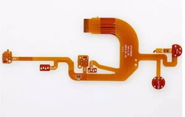
The evolution of flexible printed circuit (FPC) technology has demanded increasingly sophisticated dielectric materials and testing standards. The Institute for Printed Circuits (IPC) recognized this need when it revised IPC 4202 in 2010, releasing IPC 4202A with significant updates that reflect advances in materials science, manufacturing processes, and application requirements. This comprehensive analysis examines the key differences between these two standards and their impact on the flexible electronics industry.
Background and Context
IPC 4202, originally published in 2002, established the foundation for flexible dielectric materials used in printed circuit applications. The standard addressed the growing need for standardized testing methods and performance criteria as flexible circuits became increasingly prevalent in consumer electronics, automotive applications, and aerospace systems. However, by the mid-2000s, technological advances and industry feedback revealed gaps in the original standard that necessitated a thorough revision.
The 2010 revision, designated IPC 4202A, emerged from extensive industry collaboration and represented a significant maturation of flexible circuit dielectric standards. This update addressed emerging material technologies, refined testing methodologies, and incorporated lessons learned from nearly a decade of real-world applications.
Powered By EmbedPress
Material Classification and Categorization Updates
One of the most significant changes in IPC 4202A involves the expanded and refined material classification system. The 2002 version provided a basic framework for categorizing flexible dielectric materials, but the 2010 revision introduced a more nuanced approach that better reflects the diversity of available materials and their specific applications.
The updated standard introduced additional material categories, including specialized high-temperature polyimides, liquid crystal polymers (LCP), and advanced fluoropolymer compositions. These additions reflected the industry’s move toward more demanding applications requiring superior thermal stability, chemical resistance, and dimensional stability. The 2010 revision also provided clearer guidance on material selection criteria, helping designers match dielectric properties with specific application requirements.
Furthermore, IPC 4202A expanded the coverage of adhesive systems used in flexible circuits. While the 2002 version focused primarily on traditional acrylic and epoxy adhesives, the updated standard acknowledged the growing use of adhesiveless constructions and alternative bonding technologies. This expansion recognized the industry trend toward thinner, more reliable flexible circuits with improved electrical performance.
Enhanced Testing Methodologies
The testing procedures outlined in IPC 4202A represent a substantial improvement over the 2002 version. The updated standard incorporated more rigorous and comprehensive testing protocols that better simulate real-world operating conditions. These enhancements address several critical areas where the original standard proved insufficient.
Thermal cycling tests received significant attention in the 2010 revision. The updated procedures include more severe temperature excursions and extended cycle counts that better reflect the demanding environments encountered in automotive and aerospace applications. The standard also introduced improved sample preparation techniques and more precise measurement methods for assessing thermal-induced dimensional changes.
Electrical testing protocols underwent substantial refinement in IPC 4202A. The updated standard includes more comprehensive dielectric strength testing procedures, improved methods for measuring dielectric constant and dissipation factor across broader frequency ranges, and enhanced protocols for evaluating insulation resistance under various environmental conditions. These improvements enable more accurate prediction of electrical performance in service conditions.
Mechanical testing also received considerable enhancement. The 2010 revision includes improved tear strength testing methods, more comprehensive flexibility and bend testing protocols, and enhanced procedures for evaluating adhesion strength between layers. These updates address critical reliability concerns that emerged as flexible circuits found applications in increasingly demanding mechanical environments.
Environmental and Reliability Testing Improvements
Environmental testing represents one of the most significantly enhanced areas in IPC 4202A. The 2010 revision introduced more comprehensive humidity testing protocols that better simulate the challenging environments encountered in mobile electronics and outdoor applications. The updated standard includes extended exposure periods, more severe humidity levels, and improved methods for assessing moisture absorption and its effects on electrical and mechanical properties.
Chemical resistance testing also received substantial improvement. While the 2002 version provided basic chemical exposure testing, IPC 4202A expanded this to include a broader range of chemicals commonly encountered in manufacturing and service environments. The updated standard includes specific protocols for evaluating resistance to flux chemicals, cleaning solvents, and environmental contaminants that can affect long-term reliability.
Accelerated aging tests in the 2010 revision better reflect the increasing reliability requirements of modern applications. The updated standard includes more sophisticated aging protocols that combine multiple stressors simultaneously, providing more realistic assessments of long-term performance. These improvements enable more accurate lifetime predictions and better material selection for specific applications.
Specification Requirements and Performance Criteria
IPC 4202A introduced more stringent and comprehensive performance requirements compared to its 2002 predecessor. The updated standard established tighter tolerances for key properties such as dimensional stability, coefficient of thermal expansion, and dielectric properties. These enhanced requirements reflect the industry’s increasing demand for precision and reliability in flexible circuit applications.
The 2010 revision also introduced new performance categories that address specific application needs. High-reliability applications, such as those found in medical devices and aerospace systems, received dedicated specification requirements that ensure appropriate material selection and performance verification. Similarly, cost-sensitive consumer applications received guidance that balances performance requirements with economic considerations.
Electrical performance specifications underwent significant enhancement in IPC 4202A. The updated standard includes more comprehensive requirements for dielectric strength, insulation resistance, and dielectric properties across broader temperature and frequency ranges. These improvements ensure that materials meet the demanding electrical performance requirements of modern high-speed digital and RF applications.
Documentation and Traceability Enhancements
The 2010 revision placed greater emphasis on documentation and traceability requirements. IPC 4202A introduced more comprehensive record-keeping requirements for material qualification testing, manufacturing process controls, and quality assurance activities. These enhancements support the increasingly stringent traceability requirements found in automotive, aerospace, and medical device applications.
The updated standard also improved guidance on material data sheets and technical documentation. IPC 4202A established standardized formats for presenting material properties and test results, facilitating better communication between material suppliers, circuit manufacturers, and end users. This standardization reduces the potential for misunderstandings and ensures that critical performance information is properly communicated throughout the supply chain.
Industry Impact and Adoption Challenges
The transition from IPC 4202 to IPC 4202A presented both opportunities and challenges for the flexible circuit industry. Manufacturers needed to update their testing equipment and procedures to comply with the enhanced requirements, representing a significant investment in some cases. However, the improved testing methods and performance criteria enabled better material characterization and more reliable product development.
The updated standard also influenced material supplier development priorities. The enhanced requirements in IPC 4202A drove innovation in dielectric material formulations, leading to improved products with better thermal stability, lower moisture absorption, and enhanced reliability. This virtuous cycle of standard improvement driving material advancement has benefited the entire industry.
Future Implications and Ongoing Evolution
The successful implementation of IPC 4202A demonstrated the importance of regularly updating industry standards to keep pace with technological advancement. The improvements introduced in the 2010 revision have provided a solid foundation for continued innovation in flexible circuit dielectrics. As new applications emerge and performance requirements continue to increase, the lessons learned from the IPC 4202 to IPC 4202A transition will inform future standard development efforts.
The enhanced testing methodologies and performance requirements established in IPC 4202A have raised the overall quality and reliability of flexible circuit products. This improvement has enabled the expansion of flexible circuits into increasingly demanding applications, furthering the growth and technological advancement of the industry.
Conclusion
The evolution from IPC 4202 (2002) to IPC 4202A (2010) represents a significant advancement in flexible printed circuit dielectric standards. The updated standard addresses critical gaps in the original version while incorporating advances in materials science, testing technology, and application requirements. The enhanced testing methodologies, expanded material coverage, improved performance criteria, and better documentation requirements have strengthened the foundation for flexible circuit development and manufacturing.
These improvements have had lasting positive impacts on the industry, enabling the development of more reliable and capable flexible circuit products. As the demand for flexible electronics continues to grow across diverse applications, the robust foundation established by IPC 4202A will continue to support innovation and quality improvement in this dynamic field. The success of this standard revision demonstrates the importance of continuous improvement in industry standards to support technological advancement and market growth.
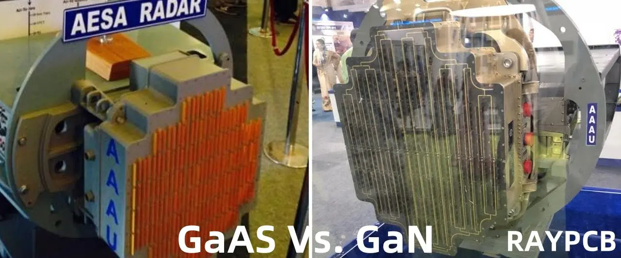
The radar technology landscape has undergone significant transformation in recent years, with two prominent technologies leading the charge: Gallium Arsenide (GaAs) and Gallium Nitride (GaN) radar systems. Understanding the fundamental differences between GAA (GaAs) and GaN radar technologies is crucial for engineers, procurement specialists, and decision-makers in defense, automotive, aerospace, and telecommunications industries.
Modern radar applications demand higher performance, improved efficiency, and enhanced reliability. As traditional silicon-based technologies reach their physical limitations, compound semiconductors like GaAs and GaN have emerged as superior alternatives, each offering unique advantages for specific applications. This comprehensive analysis explores the technical specifications, performance characteristics, cost implications, and practical applications of both technologies.
The choice between GAA and GaN radar systems significantly impacts system performance, operational costs, and long-term viability. While both technologies utilize gallium-based compounds, their distinct material properties result in vastly different capabilities and use cases. This article provides an in-depth comparison to help stakeholders make informed decisions based on their specific requirements.
Gallium Nitride (GaN) radar represents the cutting-edge of semiconductor technology in radar applications. GaN is a wide-bandgap semiconductor material that offers exceptional performance characteristics, making it ideal for high-power, high-frequency radar systems. The technology has revolutionized radar capabilities across military, commercial, and civilian applications.
GaN radar systems utilize the unique properties of gallium nitride semiconductors to achieve superior power density, efficiency, and frequency response compared to traditional technologies. The wide bandgap of GaN (approximately 3.4 eV) enables operation at higher voltages, temperatures, and frequencies while maintaining excellent efficiency and reliability.
Key Characteristics of GaN Radar
The fundamental properties of GaN make it exceptionally suitable for radar applications. The material exhibits high electron mobility, excellent thermal conductivity, and remarkable stability under extreme operating conditions. These characteristics translate into radar systems that can operate at higher power levels while maintaining consistent performance across varying environmental conditions.
GaN radar systems typically operate efficiently at frequencies ranging from L-band to Ka-band and beyond, making them versatile solutions for diverse applications. The technology’s ability to handle high power densities enables compact system designs without compromising performance, a critical advantage in space-constrained applications.
Performance Advantages of GaN Radar
GaN radar technology offers several performance advantages that make it attractive for demanding applications. The high power density capability allows for more compact antenna designs and reduced system size while maintaining or improving radar range and resolution. This is particularly valuable in airborne and space-based applications where size and weight constraints are critical.
The efficiency of GaN radar systems typically exceeds 50%, significantly higher than older technologies. This improved efficiency translates into reduced power consumption, lower heat generation, and enhanced system reliability. The reduced thermal load also simplifies cooling requirements, further contributing to system compactness and reliability.
GaN radar systems demonstrate excellent linearity characteristics, enabling advanced waveform generation and processing techniques. This capability is essential for modern radar applications that require sophisticated signal processing, electronic warfare countermeasures, and multi-function operations.
Understanding GAA (GaAs) Radar Technology
What is GAA Radar?
Gallium Arsenide (GaAs) radar technology has been a cornerstone of high-performance radar systems for several decades. GaAs is a compound semiconductor that offers superior performance compared to silicon while remaining more cost-effective than newer wide-bandgap materials. The technology has been extensively developed and optimized for radar applications, resulting in mature, reliable solutions.
GaAs-based radar systems leverage the material’s excellent electron mobility and relatively wide bandgap (1.42 eV) to achieve good performance in microwave and millimeter-wave applications. The technology has been particularly successful in applications requiring moderate power levels and excellent noise performance.
Key Characteristics of GAA Radar
GaAs radar technology is characterized by excellent noise performance, making it ideal for sensitive receiver applications and low-noise amplification. The material’s electron mobility is superior to silicon, enabling high-frequency operation with good gain and efficiency characteristics.
The maturity of GaAs technology means that manufacturing processes are well-established, resulting in consistent quality and relatively predictable costs. This maturity also translates into extensive design experience and readily available component libraries, simplifying system development and integration.
Performance Characteristics of GAA Radar
GAA radar systems excel in applications requiring excellent noise figure performance and moderate power levels. The technology is particularly well-suited for receiver front-ends, low-noise amplifiers, and mixer circuits where noise performance is critical to overall system sensitivity.
GaAs radar systems typically operate efficiently in the microwave frequency range, with good performance extending into millimeter-wave bands. While power handling capability is more limited compared to GaN, GaAs systems offer excellent linearity and stability characteristics that make them suitable for precision radar applications.
The most significant difference between GAA and GaN radar technologies lies in their power handling capabilities and efficiency characteristics. GaN radar systems can handle significantly higher power densities, typically 5-10 times greater than GaAs systems. This advantage stems from GaN’s superior thermal conductivity and higher breakdown voltage.
GaN radar efficiency typically ranges from 50-65%, while GaAs systems generally achieve 25-40% efficiency. This efficiency difference has profound implications for system design, power consumption, and thermal management. Higher efficiency translates directly into reduced power supply requirements, simplified cooling systems, and improved system reliability.
The power advantage of GaN becomes particularly pronounced at higher frequencies. While both technologies can operate at millimeter-wave frequencies, GaN maintains its power and efficiency advantages even as frequency increases, making it the preferred choice for high-frequency, high-power applications.
Frequency Response and Bandwidth
Both GAA and GaN radar technologies offer excellent frequency response characteristics, but with different strengths. GaN radar systems maintain consistent performance across broader frequency ranges, making them suitable for wideband and multi-band applications. The technology’s inherent characteristics enable operation from L-band through Ka-band and beyond with minimal performance degradation.
GaAs radar systems traditionally excel in specific frequency bands where their noise performance advantages are most pronounced. The technology is particularly effective in applications requiring exceptional sensitivity and low-noise operation, even if maximum power output is not the primary concern.
The bandwidth capabilities of both technologies are sufficient for modern radar applications, including pulse compression, frequency agility, and spread spectrum techniques. However, GaN’s broader operating bandwidth provides greater flexibility for multi-function radar systems and software-defined radio applications.
Thermal Performance and Reliability
Thermal management represents a critical differentiator between GAA and GaN radar technologies. GaN’s superior thermal conductivity (approximately 1.3 W/cm·K) compared to GaAs (0.46 W/cm·K) enables better heat dissipation and improved thermal performance. This characteristic is crucial for high-power radar applications where thermal management directly impacts system reliability and performance.
GaN radar systems can operate at higher junction temperatures while maintaining stable performance, reducing cooling requirements and enabling more compact system designs. The improved thermal performance also contributes to longer component lifetimes and enhanced system reliability.
The reliability characteristics of both technologies are excellent when properly designed and implemented. However, GaN’s ability to operate at higher temperatures and power levels while maintaining performance provides additional margin for robust system operation in challenging environments.
Cost Considerations
Cost analysis between GAA and GaN radar technologies involves multiple factors beyond initial component prices. While GaAs components are generally less expensive per unit, the total system cost comparison must consider performance capabilities, power consumption, cooling requirements, and system complexity.
GaN radar systems, despite higher initial component costs, often provide better value in high-performance applications due to their superior efficiency and power handling capabilities. The reduced power consumption and simplified cooling requirements can offset higher component costs in many applications.
The cost differential between technologies continues to narrow as GaN manufacturing volumes increase and processes mature. For many applications, the performance advantages of GaN justify any cost premium, particularly when total cost of ownership is considered.
Military and defense radar applications represent one of the most demanding environments for radar technology, requiring high performance, reliability, and adaptability. Both GAA and GaN radar technologies serve important roles in this sector, but their applications often differ based on specific requirements.
GaN radar technology has become the preferred choice for high-power military radar applications, including long-range surveillance radars, fire control systems, and active electronically scanned arrays (AESAs). The technology’s high power density enables compact, lightweight radar systems suitable for airborne platforms, ships, and mobile ground systems.
The efficiency advantages of GaN radar are particularly valuable in military applications where power generation and consumption directly impact operational capabilities. Reduced power requirements translate into longer mission endurance, reduced fuel consumption, and simplified logistics support.
GAA radar technology continues to play important roles in military applications requiring exceptional sensitivity and noise performance. Applications such as electronic warfare systems, precision tracking radars, and communication systems often benefit from GaAs technology’s superior noise characteristics.
Commercial Aviation and Air Traffic Control
Commercial aviation and air traffic control applications present unique requirements for radar technology, emphasizing reliability, precision, and cost-effectiveness. Both GAA and GaN radar technologies serve important roles in this sector, with applications ranging from weather radar to collision avoidance systems.
GaN radar technology is increasingly adopted for weather radar applications where high power and wide bandwidth are essential for accurate precipitation detection and wind measurement. The technology’s efficiency advantages also reduce operating costs for airlines and airports through lower power consumption.
Air traffic control radar systems benefit from both technologies depending on specific requirements. Primary surveillance radars often utilize GaN technology for its power and range capabilities, while secondary surveillance radars may employ GaAs technology where sensitivity and cost are primary concerns.
The reliability requirements of commercial aviation favor both technologies when properly implemented, but the simplified thermal management of GaN systems provides advantages in challenging installation environments.
Automotive Radar Systems
The automotive industry represents one of the fastest-growing markets for radar technology, driven by autonomous driving capabilities and advanced driver assistance systems (ADAS). The unique requirements of automotive applications present interesting trade-offs between GAA and GaN radar technologies.
GaN radar technology offers advantages for long-range automotive radar applications, providing the power and efficiency needed for highway-speed collision avoidance and adaptive cruise control systems. The technology’s compact size and high integration capability align well with automotive packaging constraints.
Short-range automotive radar applications, such as parking assistance and blind-spot monitoring, may benefit from GaAs technology’s cost advantages and excellent noise performance. These applications typically operate at lower power levels where GaN’s power advantages are less critical.
The automotive industry’s emphasis on cost reduction and high-volume manufacturing favors mature technologies with established supply chains. However, the performance advantages of GaN technology are driving increased adoption as system requirements become more demanding.
Telecommunications and 5G Infrastructure
Telecommunications infrastructure, particularly 5G networks, presents unique requirements for radar-like technologies used in beamforming and massive MIMO applications. While not traditional radar applications, these systems share many technical requirements with radar systems.
GaN technology has become the preferred choice for 5G base station applications due to its efficiency and power handling capabilities. The technology enables compact, efficient amplifiers that reduce operating costs and simplify installation requirements.
The integration capabilities of both technologies are important for telecommunications applications where size and cost constraints are significant. GaN’s higher integration potential and reduced component count provide advantages in system-level implementations.
Performance Metrics and Benchmarking
Power Output and Efficiency Metrics
Quantitative comparison of power output and efficiency metrics reveals the significant advantages of GaN radar over GAA radar in high-power applications. Typical GaN radar amplifiers achieve power densities of 5-10 W/mm of gate periphery, compared to 1-2 W/mm for GaAs amplifiers at similar frequencies.
Efficiency measurements consistently favor GaN technology, with practical implementations achieving 50-65% power-added efficiency compared to 25-40% for GaAs systems. This efficiency advantage becomes more pronounced at higher frequencies and power levels, making GaN the clear choice for demanding applications.
The power output capability of GaN radar systems enables new system architectures and applications that were not practical with previous technologies. High-power, compact radar systems can now be implemented in space-constrained environments while maintaining excellent performance characteristics.
Noise Figure and Sensitivity Analysis
Noise figure performance represents an area where GAA radar technology traditionally maintains advantages over GaN radar systems. GaAs low-noise amplifiers typically achieve noise figures of 0.5-1.0 dB in the microwave frequency range, compared to 1.0-2.0 dB for comparable GaN amplifiers.
However, the noise figure advantage of GaAs must be considered in the context of overall system performance. The higher power output capability of GaN systems often enables system architectures that compensate for higher noise figures through increased transmitter power and improved antenna gain.
Recent developments in GaN technology have significantly reduced the noise figure gap, with advanced GaN devices achieving noise figures approaching GaAs performance levels. This improvement, combined with GaN’s other advantages, further strengthens its position in radar applications.
Reliability and Lifetime Comparisons
Reliability analysis of GAA vs GaN radar technologies requires consideration of both inherent material properties and practical implementation factors. Both technologies demonstrate excellent reliability when properly designed and operated within specified limits.
GaN radar technology’s ability to operate at higher temperatures and power levels while maintaining performance provides additional reliability margin. The reduced thermal stress on components contributes to extended operational lifetimes and improved mean time between failures (MTBF).
Accelerated life testing of both technologies under realistic operating conditions shows comparable reliability characteristics when systems are properly designed. However, GaN’s superior thermal performance provides advantages in challenging operating environments where thermal stress is a primary failure mechanism.
Manufacturing and Production Considerations
Fabrication Processes and Yield
The manufacturing processes for GAA and GaN radar technologies differ significantly, impacting cost, yield, and scalability. GaAs technology benefits from decades of process development and optimization, resulting in mature manufacturing processes with high yields and predictable quality.
GaN radar technology manufacturing has progressed rapidly but remains more challenging than GaAs production. The growth of high-quality GaN epitaxial layers requires precise control of multiple parameters, and device fabrication involves several complex process steps.
Yield considerations favor GaAs technology for high-volume, cost-sensitive applications. However, GaN manufacturing yields continue to improve as processes mature and production volumes increase. The performance advantages of GaN often justify lower yields in demanding applications.
Supply Chain and Availability
Supply chain considerations play important roles in technology selection for radar applications. GaAs technology benefits from an established, mature supply chain with multiple suppliers and standardized processes. This maturity provides supply security and competitive pricing for high-volume applications.
GaN radar technology supply chains are developing rapidly but remain more limited than GaAs alternatives. However, significant investments in GaN manufacturing capacity are expanding availability and reducing supply chain risks.
The strategic importance of GaN technology has led to substantial government and industry investments in manufacturing capability, particularly in North America, Europe, and Asia. These investments are rapidly improving GaN availability and reducing dependence on limited supply sources.
Quality Control and Testing
Quality control and testing requirements differ between GAA and GaN radar technologies due to their distinct characteristics and failure modes. Both technologies require comprehensive testing to ensure performance and reliability, but the specific test requirements vary.
GaN radar devices require careful attention to thermal characteristics and high-power operation during testing. The technology’s ability to handle high power levels necessitates specialized test equipment and procedures to verify performance under realistic operating conditions.
GaAs testing procedures are well-established and standardized across the industry. The maturity of the technology has led to comprehensive understanding of failure modes and appropriate test methodologies to ensure quality and reliability.
Economic analysis of GAA vs GaN radar technologies must consider multiple cost factors beyond initial component prices. While GaAs components typically cost less per unit, total system costs depend on performance requirements, system complexity, and operational considerations.
GaN radar systems often require higher initial investment due to component costs and potentially more complex system integration. However, these costs must be evaluated against the performance benefits and operational advantages that GaN technology provides.
The cost gap between technologies continues to narrow as GaN manufacturing scales up and processes mature. Volume production and competition among suppliers are driving down GaN costs while performance advantages remain constant or improve.
Total Cost of Ownership Analysis
Total cost of ownership (TCO) analysis reveals that GaN radar systems often provide superior economic value despite higher initial costs. The efficiency advantages of GaN technology translate directly into reduced operational costs through lower power consumption and simplified cooling requirements.
Maintenance and support costs may favor GaN systems due to their improved reliability and reduced thermal stress. Fewer component failures and longer operational lifetimes contribute to lower lifecycle costs in many applications.
The compact size and reduced complexity of GaN radar systems can also reduce installation and infrastructure costs. Simplified power distribution, cooling systems, and mechanical structures offset higher component costs in many installations.
Return on Investment Projections
Return on investment (ROI) analysis for GaN radar technology depends heavily on application requirements and operational factors. Applications requiring high performance, efficiency, or compact size typically show favorable ROI for GaN technology within 2-5 years.
The improving cost structure of GaN technology enhances ROI projections over time. As manufacturing scales up and costs decline, the economic advantages of GaN radar systems become more compelling across a broader range of applications.
Long-term ROI considerations must also account for technology evolution and obsolescence risks. GaN technology’s position as the leading-edge solution provides better protection against technological obsolescence compared to mature technologies.
Future Trends and Technological Evolution
Emerging GaN Radar Innovations
The future of GaN radar technology includes several promising developments that will further enhance its capabilities and expand its applications. Advanced device structures, including enhancement-mode devices and monolithic microwave integrated circuits (MMICs), are improving performance while reducing system complexity.
Integration advances are enabling complete radar front-ends on single GaN chips, dramatically reducing size, cost, and complexity. These integrated solutions maintain the performance advantages of GaN technology while approaching the cost structures traditionally associated with silicon-based solutions.
Packaging innovations are addressing thermal management challenges and enabling even higher power densities. Advanced thermal interface materials and three-dimensional packaging approaches are pushing the boundaries of what’s possible with GaN radar technology.
GAA Technology Roadmap
While GaN technology captures much attention, GaAs radar technology continues to evolve and find new applications. Advanced GaAs processes are improving noise performance and frequency capabilities, maintaining the technology’s relevance in specialized applications.
Integration developments in GaAs technology focus on system-on-chip solutions that combine multiple functions on single substrates. These developments help GaAs technology maintain cost competitiveness while leveraging its noise performance advantages.
Niche applications continue to drive GaAs technology development, particularly in areas where ultimate sensitivity is more important than power output. These applications ensure continued investment in GaAs technology advancement.
Market Predictions and Industry Outlook
Market analysis predicts continued growth for both GAA and GaN radar technologies, with GaN capturing an increasing share of high-performance applications. The expanding automotive radar market represents a significant growth opportunity for both technologies.
Defense spending on advanced radar systems favors GaN technology due to its performance advantages and strategic importance. Government investments in GaN manufacturing capability are expected to accelerate technology adoption and reduce costs.
The 5G infrastructure buildout and emerging 6G technologies create additional markets for GaN technology, although these applications differ from traditional radar uses. The synergy between telecommunications and radar applications benefits GaN technology development.
Technical Implementation Guidelines
System Design Considerations
Implementing GAA or GaN radar technology requires careful consideration of system-level requirements and constraints. The choice between technologies should be based on thorough analysis of performance requirements, cost constraints, and operational considerations.
GaN radar system design must account for the technology’s high power density and thermal characteristics. Proper thermal management is essential to realize GaN’s performance advantages while maintaining reliability. System designers must consider heat sinking, airflow, and component placement to optimize thermal performance.
Power supply design differs significantly between GAA and GaN radar systems due to their different efficiency characteristics and voltage requirements. GaN systems typically require higher supply voltages but consume less current, impacting power supply design and distribution systems.
Integration and Compatibility Issues
Integration considerations play important roles in technology selection and system design. Both GAA and GaN technologies can be integrated with digital signal processing and control systems, but the specific requirements and interfaces may differ.
Legacy system compatibility may favor GaAs technology in upgrade applications where existing infrastructure and interfaces must be maintained. However, the performance advantages of GaN technology often justify more extensive system modifications.
Test and measurement equipment compatibility must be considered when implementing either technology. High-power GaN systems may require specialized test equipment and procedures that differ from those used with GaAs systems.
Performance Optimization Strategies
Optimizing performance in GAA and GaN radar systems requires different approaches based on each technology’s characteristics. GaN systems benefit from optimization strategies that leverage high power density and efficiency, while GaAs systems may focus on noise optimization and linearity.
Bias point optimization differs significantly between technologies. GaN devices typically operate in different bias regimes compared to GaAs devices, requiring different optimization approaches to achieve optimal performance.
Matching network design and optimization represent critical aspects of both technologies but with different emphasis. GaN systems must handle higher power levels and wider bandwidths, while GaAs systems may prioritize noise matching and stability.
Conclusion and Recommendations
Summary of Key Differences
The comparison between GAA and GaN radar technologies reveals distinct advantages and applications for each technology. GaN radar systems excel in high-power, high-efficiency applications where performance is the primary concern. The technology’s superior power density, efficiency, and thermal characteristics make it ideal for demanding military, aerospace, and high-performance commercial applications.
GAA radar technology maintains advantages in cost-sensitive applications and those requiring exceptional noise performance. The maturity of GaAs technology provides supply chain security and predictable costs that remain attractive for many applications.
The choice between technologies should be based on comprehensive analysis of requirements, including performance specifications, cost constraints, and operational considerations. Both technologies will continue to serve important roles in the radar industry, with their applications determined by specific system requirements.
Decision-Making Framework
Selecting between GAA and GaN radar technologies requires systematic evaluation of multiple factors. Performance requirements represent the primary consideration, with GaN technology favored for high-power applications and GaAs for low-noise applications.
Cost analysis must consider total cost of ownership rather than just initial component costs. Applications with high operational costs or demanding size constraints often favor GaN technology despite higher initial investment.
Technical risk assessment should consider technology maturity, supply chain security, and long-term viability. GaAs technology offers lower technical risk for many applications, while GaN provides better future-proofing for performance-critical systems.
Future Outlook and Strategic Recommendations
The future of radar technology will see continued adoption of GaN technology in high-performance applications, driven by its superior capabilities and improving cost structure. Organizations should develop GaN expertise and supply relationships to prepare for this transition.
GAA technology will continue to serve important roles in cost-sensitive and noise-critical applications. Maintaining capabilities in both technologies provides flexibility to optimize solutions for specific requirements.
Investment in advanced radar technologies should consider both current needs and future requirements. The rapid evolution of radar applications, particularly in automotive and telecommunications sectors, creates opportunities for both technologies but with different emphasis.
Strategic planning should account for the convergence of radar and communication technologies, particularly in 5G and future wireless systems. This convergence favors technologies with broad bandwidth and high integration capabilities, generally favoring GaN solutions.
The geopolitical importance of semiconductor technology adds strategic considerations to technology selection. Supply chain security and domestic manufacturing capability are increasingly important factors in technology decisions, particularly for defense and critical infrastructure applications.
Organizations should develop comprehensive technology roadmaps that consider both GAA and GaN technologies while preparing for future innovations. The rapid pace of semiconductor development ensures that today’s decisions will impact competitiveness for years to come, making strategic technology selection more critical than ever.
Modern livestock management has evolved significantly with the integration of digital technologies, transforming traditional farming practices into sophisticated, data-driven operations. Among the most impactful innovations is the development of automated livestock counting systems integrated directly into fencing infrastructure. These systems represent a convergence of precision agriculture, Internet of Things (IoT) technology, and advanced sensor networks, all orchestrated through carefully designed printed circuit boards (PCBs) that serve as the technological backbone of smart fencing solutions.
The need for automated livestock counting has emerged from several critical challenges facing contemporary livestock operations. Manual counting methods are labor-intensive, prone to human error, and often impractical for large-scale operations or remote locations. Traditional counting systems struggle with accuracy in varying environmental conditions, while the economic pressures on agricultural operations demand more efficient resource utilization and real-time operational insights. Automated counting modules embedded within fencing systems address these challenges by providing continuous, accurate monitoring without requiring additional infrastructure or significant changes to existing farm layouts.
The integration of counting modules into fencing systems offers unique advantages over standalone monitoring solutions. Fencing represents existing infrastructure that livestock must interact with regularly, making it an ideal platform for sensor deployment. Animals naturally pass through fence gates, creating predictable monitoring points that eliminate the need for additional structural installations. This integration approach reduces deployment costs, minimizes visual impact on pastoral landscapes, and leverages the power infrastructure often already present in modern fencing systems.
The automated livestock counting module represents a sophisticated electronic system requiring careful consideration of multiple interconnected subsystems. The core architecture centers around a microcontroller unit (MCU) that coordinates sensor inputs, processes counting algorithms, manages data storage, and handles communication protocols. Modern implementations typically employ ARM Cortex-M series processors or similar low-power, high-performance microcontrollers capable of real-time processing while maintaining extended battery life in remote applications.
Sensor integration forms the cornerstone of accurate livestock counting, with multiple sensing modalities often employed to ensure reliability across diverse environmental conditions. Infrared break-beam sensors provide reliable detection for animals passing through defined spaces, while passive infrared (PIR) sensors detect heat signatures and movement patterns. Ultrasonic sensors offer distance measurement capabilities, enabling the system to distinguish between different animal sizes and identify multiple animals passing simultaneously. Advanced implementations incorporate computer vision modules with low-power image processors, enabling sophisticated animal recognition and behavioral analysis.
Power management represents a critical design consideration, particularly for remote fencing applications where grid power may be unavailable. The PCB design must accommodate multiple power sources, including solar panels, rechargeable battery systems, and potentially energy harvesting from animal movement or environmental sources. Power management integrated circuits (PMICs) regulate voltage levels, manage charging cycles, and implement power-saving modes to extend operational life between maintenance intervals.
Communication capabilities enable integration with broader farm management systems and remote monitoring platforms. Modern livestock counting modules incorporate multiple communication protocols, including Wi-Fi for local area networks, cellular connectivity for wide-area coverage, and low-power wide-area network (LPWAN) technologies such as LoRaWAN for extended range with minimal power consumption. Bluetooth Low Energy (BLE) provides local connectivity for configuration and maintenance operations.
PCB Design Considerations
The printed circuit board design for livestock counting modules must address unique challenges associated with outdoor agricultural environments. Environmental protection represents the primary design consideration, as these systems must operate reliably in conditions ranging from extreme temperatures to high humidity, dust exposure, and potential chemical contamination from agricultural processes. The PCB layout must minimize moisture ingress paths, incorporate appropriate conformal coatings, and ensure thermal management across wide temperature ranges.
Signal integrity becomes particularly crucial when dealing with sensitive analog sensor inputs and high-frequency digital communications. Proper ground plane design, controlled impedance routing, and electromagnetic interference (EMI) shielding protect sensitive circuits from the electrically noisy environment typical of agricultural settings. Power supply noise, generated by motor-driven equipment and variable frequency drives common in modern farming operations, requires careful filtering and isolation techniques implemented at the PCB level.
Component selection for livestock counting modules prioritizes reliability, environmental tolerance, and long-term availability. Industrial-grade components with extended temperature ranges, enhanced moisture resistance, and proven reliability in harsh environments form the foundation of robust designs. Automotive-qualified components often provide excellent alternatives, as they undergo rigorous environmental testing and offer long-term supply chain stability crucial for agricultural applications with extended service lives.
The mechanical design of the PCB must accommodate installation within fencing systems while providing access for maintenance and configuration. Modular connector systems enable field replacement of sensors or communication modules without complete system replacement. The form factor must fit within standard fence post dimensions or gate mechanisms while maintaining structural integrity under mechanical stress from animal contact or weather exposure.
Sensor Integration and Processing
Effective livestock counting requires sophisticated sensor fusion algorithms implemented on the PCB’s processing platform. Multiple sensor inputs must be correlated and processed in real-time to provide accurate count data while filtering false positives from environmental factors. The PCB design must provide adequate analog-to-digital conversion capabilities with sufficient resolution and sampling rates to capture rapid animal movements while maintaining low power consumption.
Digital signal processing (DSP) capabilities, either through dedicated DSP processors or MCUs with integrated DSP functionality, enable implementation of advanced filtering algorithms. These algorithms differentiate between livestock and other moving objects such as wildlife, farm equipment, or environmental factors like moving vegetation. Machine learning inference capabilities, increasingly available in embedded processors, enable adaptive counting algorithms that improve accuracy over time through pattern recognition and behavioral analysis.
Sensor calibration and self-diagnostic capabilities require PCB designs that support precision voltage references, temperature compensation, and automated testing routines. Built-in test (BIT) functionality enables remote diagnosis of sensor performance and early detection of component degradation before complete system failure. This predictive maintenance capability reduces operational downtime and extends system service life.
The timing precision required for accurate counting necessitates high-quality clock sources and careful attention to timing distribution across the PCB. Crystal oscillators with appropriate temperature stability and aging characteristics ensure consistent timing performance across the operational temperature range. Clock domain crossing techniques become important when interfacing sensors operating at different sampling rates or communication protocols with varying timing requirements.
Communication and Connectivity
Modern livestock counting systems must integrate seamlessly with existing farm management infrastructure and provide reliable data transmission to centralized monitoring systems. The PCB design must accommodate multiple communication interfaces while managing power consumption and maintaining reliability in challenging RF environments. Agricultural settings often present unique RF challenges, including interference from electrical equipment, metallic structures, and varying terrain that affects signal propagation.
Cellular connectivity provides the most robust solution for remote monitoring, but requires careful antenna design and power management to ensure reliable operation. The PCB must integrate cellular modem modules with appropriate power sequencing, SIM card interfaces, and antenna matching networks optimized for the specific frequency bands used in the deployment region. Backup communication methods, such as satellite connectivity for extremely remote locations, may require additional RF design considerations.
Local area networking capabilities enable integration with on-farm systems such as existing Wi-Fi networks or dedicated agricultural IoT networks. The PCB design must support multiple networking protocols while maintaining electromagnetic compatibility with other farm equipment. Edge computing capabilities allow local data processing and decision-making, reducing communication bandwidth requirements and improving system responsiveness.
Data security and encryption capabilities must be implemented at the hardware level to protect sensitive operational information. Secure boot processes, hardware security modules (HSMs), and encrypted communication protocols protect against unauthorized access and data tampering. These security features require dedicated processing capabilities and secure storage elements integrated into the PCB design.
Manufacturing and Assembly Considerations
The manufacturing of PCBs for livestock counting modules requires specialized processes and quality control measures appropriate for harsh environment applications. Surface mount technology (SMT) assembly processes must accommodate components with enhanced environmental ratings while maintaining high reliability standards. Solder joint reliability becomes critical for long-term operation in temperature cycling and vibration environments typical of agricultural applications.
Conformal coating application protects assembled PCBs from moisture, chemical exposure, and environmental contamination. The coating selection must balance protection levels with thermal dissipation requirements and component accessibility for potential repairs. Advanced coating materials such as parylene provide superior protection but require specialized application equipment and processes.
Quality assurance processes for agricultural electronics must address the unique failure modes associated with outdoor operation. Accelerated aging tests, thermal cycling, humidity exposure, and vibration testing validate design robustness before deployment. In-circuit testing (ICT) and functional testing procedures verify proper assembly and initial calibration of sensor systems.
Supply chain management for agricultural electronics requires consideration of component lifecycle and availability over extended product lifespans. Agricultural equipment typically operates for decades, necessitating component selection strategies that ensure long-term availability or provide clear obsolescence management pathways. Strategic component inventory management and supplier diversification protect against supply chain disruptions.
Environmental Protection and Reliability
Environmental protection strategies for livestock counting PCBs must address multiple simultaneous stressors typical of agricultural environments. Temperature extremes ranging from arctic conditions to desert heat require component derating and thermal management strategies. Humidity control through desiccants, vapor barriers, and drainage design prevents condensation and corrosion within enclosures.
Chemical resistance becomes important in environments where cleaning agents, pesticides, and animal waste products may contact electronic systems. Materials selection for PCB substrates, component packages, and protective coatings must consider chemical compatibility with anticipated exposure scenarios. Galvanic corrosion prevention requires careful consideration of dissimilar metal combinations and appropriate surface treatments.
Mechanical protection strategies address impact resistance, vibration immunity, and structural integrity under varying mechanical loads. Gate-mounted systems experience repetitive mechanical stress from opening and closing operations, while fence-mounted systems must withstand animal contact and weather-induced movement. Shock mounting, flexible interconnections, and robust mechanical design prevent stress-related failures.
Lightning protection and electrical transient suppression protect sensitive electronics from the high-energy transients common in outdoor agricultural environments. Surge protection devices, proper grounding strategies, and isolation techniques prevent damage from nearby lightning strikes or electrical equipment switching transients. These protection systems must be integrated into the PCB design without compromising normal operation or adding excessive cost.
Future Developments and Integration Opportunities
The evolution of automated livestock counting systems continues toward increased sophistication and integration with broader precision agriculture platforms. Artificial intelligence capabilities, enabled by increasingly powerful embedded processors, will provide enhanced animal recognition, behavioral analysis, and predictive insights. Machine learning algorithms will adapt to specific farm conditions and animal populations, improving accuracy and reducing false positives over time.
Integration with blockchain technology offers opportunities for secure, immutable livestock tracking and supply chain verification. PCB designs must accommodate the cryptographic processing requirements for blockchain participation while maintaining power efficiency and real-time performance. Smart contracts and automated compliance reporting capabilities will streamline regulatory compliance and enhance traceability throughout the livestock supply chain.
Advanced sensor technologies, including miniaturized radar systems, LiDAR sensors, and hyperspectral imaging, will provide enhanced monitoring capabilities. These technologies require sophisticated PCB designs with high-speed digital processing, precision analog circuits, and advanced power management. The integration of these sensors into existing fencing infrastructure will demand innovative mechanical and electrical design approaches.
Edge computing and fog computing architectures will enable distributed intelligence throughout livestock operations. PCB designs must support local processing capabilities while maintaining connectivity to cloud-based analytics platforms. This distributed approach reduces latency, improves system reliability, and enables autonomous operation during communication outages.
Conclusion
The development of automated livestock counting modules represents a significant advancement in precision agriculture technology, with PCB design and manufacturing playing a crucial role in system success. The unique requirements of agricultural environments demand sophisticated engineering approaches that balance performance, reliability, and cost-effectiveness. Successful implementations require careful consideration of environmental protection, power management, sensor integration, and communication capabilities, all orchestrated through well-designed printed circuit boards.
The integration of these systems into existing fencing infrastructure provides a cost-effective deployment strategy that leverages existing agricultural infrastructure while providing valuable operational insights. As technology continues to evolve, these systems will become increasingly sophisticated, providing enhanced analytics capabilities and integration with broader farm management platforms.
The future of automated livestock counting lies in the continued miniaturization of sensors, advancement of processing capabilities, and integration with artificial intelligence systems. PCB designers and manufacturers must continue to innovate in materials science, manufacturing processes, and design methodologies to meet the evolving demands of precision agriculture. The success of these systems will ultimately depend on their ability to provide reliable, accurate, and cost-effective solutions that enhance livestock management while withstanding the challenges of agricultural environments.
IPC-J-STD-001 stands as the most recognized and trusted standard for soldering in the electronics industry worldwide. This comprehensive standard defines material specifications, process requirements, and acceptability criteria for producing high-quality soldered electrical and electronic assemblies. Whether you’re a quality engineer, process technician, or electronics manufacturer, understanding IPC-J-STD-001 is essential for ensuring reliable, defect-free electronic products.
What is IPC-J-STD-001?
IPC-J-STD-001, officially titled “Requirements for Soldered Electrical and Electronic Assemblies,” was developed in 1992 and replaced the earlier document IPC-S-815. As of 2024, the latest version is IPC-J-STD-001J, published in March 2024, which incorporates input and expertise from participants in 27 countries.
This joint industry standard serves as the definitive guide for electronics manufacturers, establishing minimum requirements for materials, methods, and acceptance criteria for soldered connections. The standard describes materials, methods and verification criteria for producing high-quality soldered leaded and lead-free interconnections while emphasizing process control.
Key Features of IPC-J-STD-001J
The 2024 revision includes several important updates:
Enhanced X-ray Inspection Guidance: Provides comprehensive guidance on using x-ray technology to inspect through-hole solder conditions that are not visible by other inspection methods
Global Industry Input: Developed with contributions from 27 countries
Lead-free and Leaded Solder Requirements: Covers both traditional and modern soldering materials
Process Control Emphasis: Focuses on maintaining consistent quality through proper process management
The standard outlines necessary materials for producing electronic assemblies, including solders, fluxes, and cleaning agents, with specific requirements for composition and properties of solders used in different applications. Key material requirements include:
Lead-Free Solder Alloys:
SAC (Tin-Silver-Copper) alloys
Bismuth-containing alloys for low-temperature applications
Process control is fundamental to IPC-J-STD-001, with manufacturers required to employ adequate methods for controlling production processes, especially for Class 2 and 3 products where documentation in work instructions or control plans is mandatory.
The standard outlines instructions for production and inspection of Through-Hole Technology assemblies, encompassing hole preparation, component insertion, wave soldering, and inspection criteria.
IPC provides formal classroom training and certification programs with three levels of certification:
Certified IPC Specialist (CIS):
Assembly operators
Quality staff
Inspection personnel
Process engineers
Certified Standards Expert (CSE):
Advanced knowledge requirements
Conflict resolution capabilities
Staff liaison responsibilities
Technical leadership roles
Certified IPC Trainer (CIT):
Internal training delivery
Curriculum development
Assessment capabilities
Continuous improvement
Training Benefits
Electronic manufacturing organizations can save costs by training staff for specific requirements, while IPC-J-STD-001 certification enables companies to deliver better customer satisfaction by following industry-accepted quality control standards.
Implementation Best Practices
Getting Started with IPC-J-STD-001
Step 1: Assessment and Planning
Current process evaluation
Gap analysis
Resource allocation
Timeline development
Step 2: Personnel Training
Identify training needs
Schedule certification programs
Implement hands-on training
Establish competency verification
Step 3: Process Documentation
Work instruction development
Quality control procedures
Inspection criteria establishment
Record keeping systems
Step 4: Equipment and Materials
Equipment calibration
Material qualification
Supplier verification
Inventory management
Common Implementation Challenges
Personnel Resistance:
Change management strategies
Communication importance
Training effectiveness
Motivation techniques
Cost Considerations:
Initial investment requirements
Long-term cost benefits
ROI calculations
Budget planning
Technical Complexity:
Process optimization
Equipment integration
Quality system alignment
Continuous improvement
Relationship with Other IPC Standards
IPC-A-610: Electronic Assembly Acceptance
While both IPC-A-610 and J-STD-001 emphasize the soldering process, IPC-A-610 is used for electronic assembly acceptance and provides detailed information and images for board inspection procedures, whereas J-STD-001 defines materials and processes for soldering to ensure quality solder joints.
IPC-A-600: Printed Board Acceptability
IPC-A-600 has set the standard for PCB workmanship quality with comprehensive acceptance criteria for target, acceptable and nonconforming conditions on bare printed boards.
IPC/WHMA-A-620: Cable and Wire Harness Assemblies
This standard provides requirements and acceptance criteria for cable and wire harness assemblies, complementing J-STD-001’s coverage of electronic assemblies.
Industry Applications and Benefits
Aerospace and Defense
Critical Requirements:
Military specifications compliance
Reliability in extreme conditions
Traceability requirements
Quality documentation
Space Applications: IPC has issued the J-STD-001ES standard for space addendum application, which includes specific process requirements such as red plague corrosion control plans for silver-coated copper conductors.
IPC-J-STD-001 remains the definitive standard for soldering in electronics manufacturing, providing the foundation for producing reliable, high-quality electronic assemblies. The standard is valuable for ensuring reliability, consistency, and quality of soldered electronic assemblies, which are critical in industries such as aerospace, automotive, consumer electronics, and telecommunications.
As the electronics industry continues to evolve with new technologies and materials, IPC-J-STD-001 adapts to meet emerging challenges while maintaining its core mission of ensuring soldering excellence. The standard emphasizes process control and defines industry-level requirements for various electronic products, helping organizations achieve excellence in hand soldering, electronics assembly, and inspection.
For organizations committed to manufacturing excellence, implementing IPC-J-STD-001 is not just a quality requirement—it’s a competitive advantage that ensures customer satisfaction, reduces defects, and builds long-term reliability into every product. Whether you’re beginning your journey with IPC standards or looking to upgrade to the latest revision, IPC-J-STD-001J provides the roadmap for soldering success in today’s demanding electronics marketplace.
The investment in IPC-J-STD-001 compliance pays dividends through reduced rework, improved customer satisfaction, enhanced product reliability, and the confidence that comes from following globally recognized best practices. As electronics become increasingly complex and critical to our daily lives, the importance of proper soldering standards has never been greater.
The ESP8266 has revolutionized the world of Wi-Fi IoT projects, becoming the go-to choice for makers, hobbyists, and professionals alike. This tiny yet powerful esp8266 wifi module has democratized Internet of Things development by providing affordable, reliable Wi-Fi connectivity that was once exclusive to expensive industrial solutions.
Since its introduction by Espressif Systems, the esp wifi chip has sparked an unprecedented boom in DIY smart home projects, environmental monitoring systems, and connected device prototypes. What makes the esp module so compelling is its perfect balance of functionality, affordability, and ease of use – factors that have made it the backbone of countless IoT innovations worldwide.
The ESP8266’s popularity stems from its impressive feature set packed into a compact form factor. With built-in Wi-Fi capabilities, adequate processing power, and multiple GPIO pins, this microcontroller can handle everything from simple sensor readings to complex web server operations. The vibrant ecosystem surrounding the ESP8266 includes popular development boards like the NodeMCU, Wemos D1 Mini, and the compact ESP-01, each designed to make Wi-Fi connectivity accessible to developers of all skill levels.
As IoT continues to reshape industries from agriculture to healthcare, the ESP8266 remains at the forefront of this transformation. Its low power consumption makes it ideal for battery-powered applications, while its robust Wi-Fi performance ensures reliable connectivity in demanding environments. Whether you’re building a smart irrigation system, home security network, or industrial monitoring solution, the ESP8266 provides the foundation for bringing your connected device ideas to life.
The chip’s compatibility with familiar development environments like Arduino IDE has lowered the barrier to entry for IoT development. This accessibility, combined with extensive community support and comprehensive documentation, explains why the ESP8266 continues to be the first choice for Wi-Fi-enabled projects. Even with newer alternatives like the ESP32 available, the ESP8266’s proven reliability and cost-effectiveness ensure its continued relevance in the rapidly evolving IoT landscape.
The ESP8266is a low-cost Wi-Fi microcontroller chip developed by Espressif Systems that has become synonymous with affordable IoT connectivity. At its core, the esp8266ex features a 32-bit Xtensa LX106 processor running at 80MHz (overclockable to 160MHz), coupled with integrated 802.11 b/g/n Wi-Fi capabilities. This combination provides developers with both computational power and wireless connectivity in a single, compact package.
The architecture of the esp8266mod is designed for efficiency and versatility. The chip includes 64KB of instruction RAM, 96KB of data RAM, and external flash memory support ranging from 512KB to 16MB depending on the specific module variant. This memory configuration allows the ESP8266 to run complex applications while maintaining its low-power profile, making it suitable for battery-operated IoT devices that need to operate for months or even years on a single charge.
One common misconception involves the term esp2866, which is actually a typographical error for ESP8266. The correct designation is ESP8266, and various modules like the esp8266 mini variants maintain this naming convention while offering different form factors and pin configurations to suit diverse project requirements.
Espressif Systems introduced the ESP8266 in 2014, initially targeting the Chinese market before its global adoption exploded in 2015. The chip’s development history reflects Espressif’s commitment to democratizing IoT connectivity by providing enterprise-grade Wi-Fi capabilities at consumer-friendly prices. This strategic approach disrupted the embedded Wi-Fi market, which had previously been dominated by expensive solutions from established semiconductor companies.
Understanding the relationship between ESP8266 variants is crucial for selecting the right chip for your project. The esp8285 represents an integrated version of the ESP8266 with 1MB of flash memory built directly into the package, eliminating the need for external flash storage. This integration makes the ESP8285 more compact but less flexible in terms of memory expansion.
The comparison between esp8266 esp32 chips reveals important distinctions for project planning. While the esp32 esp8266 discussion often focuses on the ESP32’s superior processing power and Bluetooth connectivity, the ESP8266 maintains advantages in power efficiency, cost-effectiveness, and proven stability for Wi-Fi-only applications. The ESP32 features dual-core processing and additional peripherals, but these enhancements come with increased power consumption and complexity that may be unnecessary for simpler IoT projects.
The ESP8266’s Wi-Fi implementation supports multiple connection modes, including station mode for connecting to existing networks, access point mode for creating its own network, and a combined mode that enables both simultaneously. This flexibility allows developers to create sophisticated networking topologies, from simple sensor nodes that report to cloud services to mesh networks that can extend Wi-Fi coverage across large areas.
The ESP8266 ecosystem encompasses numerous module variants and development boards, each optimized for specific use cases and project requirements. Understanding these options is essential for selecting the most appropriate hardware for your IoT applications.
ESP-01 and ESP-01S Series
The esp 01 represents the most compact and cost-effective entry point into ESP8266 development. The original esp 01s module features a minimal pin count with only GPIO0, GPIO2, TX, RX, VCC, GND, CH_PD, and RST accessible through its 8-pin header. Despite this limitation, the esp8266 esp 01 has found widespread use in applications where space constraints are paramount and only basic I/O functionality is required.
The esp01s variant improves upon the original design with better antenna performance and more reliable operation. The esp 01 8266 modules are particularly popular for retrofitting existing devices with Wi-Fi connectivity due to their small footprint and low cost. However, developers must work within the constraints of limited GPIO availability, making these modules best suited for simple sensor readings or relay control applications.
ESP-07 and ESP-07S with External Antenna Support
The esp 07 and esp 07s modules address the antenna limitations of smaller variants by providing both onboard ceramic antenna and external antenna connector options. This dual-antenna approach makes these modules ideal for applications requiring extended Wi-Fi range or operation in challenging RF environments. The additional GPIO pins compared to ESP-01 modules provide more flexibility for interfacing with sensors and actuators.
ESP-12 Series: Enhanced GPIO and Flash Memory
The ESP-12 family, including esp 12, esp 12e, and esp 12f variants, represents a significant step up in capability and convenience. The esp8266 12f and esp8266 12e modules feature more accessible GPIO pins, larger onboard flash memory options, and improved antenna designs. These modules strike an excellent balance between functionality and cost, making them popular choices for prototype development and small-scale production.
The ESP-12F variant includes additional improvements in antenna design and pin layout that enhance both performance and ease of use. The extra GPIO pins available on these modules enable more complex projects involving multiple sensors, displays, and communication interfaces without requiring external multiplexers or I/O expanders.
Wemos D1 Series: Arduino-Compatible Form Factors
The wemos d1 mini has achieved legendary status among ESP8266 development boards due to its compact size and Arduino Uno-compatible pin spacing. The wemos d1 mini pro extends this design with additional features like external antenna connector and more robust power regulation. The wemos mini form factor has inspired countless shield designs, creating an ecosystem of stackable modules for rapid prototyping.
The evolution from wemos d1 to wemos d1 r1 and wemos d1 r2 versions reflects continuous improvements in USB connectivity, power management, and build quality. The d1 mini and d1 mini pro variants maintain the popular compact form factor while incorporating lessons learned from earlier designs. The esp d1 mini nomenclature is sometimes used interchangeably with Wemos D1 Mini, reflecting the board’s association with ESP8266 development.
The wemos esp8266 boards have become synonymous with reliable, easy-to-use ESP8266 development platforms. The esp8266 d1 mini format’s popularity has led to numerous compatible boards from various manufacturers, creating a de facto standard for compact ESP8266 development boards.
NodeMCU: The Developer-Friendly Standard
The nodemcu platform revolutionized ESP8266 development by providing a complete development board with USB connectivity, voltage regulation, and breadboard-friendly pin layout. The nodemcu esp8266 boards come in several versions, with nodemcu v3, lolin nodemcu v3, nodemcu amica, and nodemcu v2 being the most common variants. Each version offers slight improvements in layout, components, or build quality while maintaining compatibility with the established NodeMCU pinout.
The nodemcu 8266 designation emphasizes the ESP8266-based nature of these boards, distinguishing them from ESP32-based NodeMCU variants. The node mcu8266 boards have become the de facto standard for ESP8266 education and prototyping due to their plug-and-play nature and extensive documentation.
ESP32-Based Alternatives
While this guide focuses on ESP8266, understanding ESP32 alternatives helps inform hardware selection decisions. The espwroom32 and other esp32 module variants offer increased processing power, Bluetooth connectivity, and more GPIO pins at the cost of higher power consumption and increased complexity.
The node mcu esp 32, node mcu esp32s, node mcu 32s, and esp32 node mcu boards extend the familiar NodeMCU form factor to ESP32 hardware. The esp32 8266 comparison often comes down to project requirements: choose ESP8266 for simple, power-efficient Wi-Fi applications, and ESP32 for projects requiring additional processing power, Bluetooth, or numerous GPIO pins. The wifi esp32 capabilities surpass ESP8266 in raw performance but may be overkill for many IoT applications.
Getting Started: Programming ESP8266 with Arduino IDE
ESP8266 PCB Moudle
Setting up your development environment for ESP8266 programming through Arduino IDE is straightforward and provides access to the familiar Arduino programming model. This approach makes ESP8266 development accessible to anyone with basic Arduino experience while leveraging the extensive Arduino library ecosystem.
Begin by installing the ESP8266 board package in Arduino IDE through the Board Manager. Navigate to File > Preferences and add the ESP8266 board package URL to the Additional Board Manager URLs field. After updating the board manager list, search for “ESP8266” and install the community-maintained package that provides support for various ESP8266 development boards.
The arduino ide nodemcu integration is seamless once the board package is installed. Select your specific board variant from the Tools > Board menu – options include NodeMCU variants, Wemos D1 boards, and generic ESP8266 modules. The esp8266 ide arduino combination provides access to specialized libraries and examples designed specifically for ESP8266 hardware.
Connecting your esp8266 arduino development board varies by model, but most modern boards like NodeMCU and Wemos D1 Mini include USB-to-serial converters for direct computer connection. The arduino esp8266 nodemcu setup requires selecting the correct COM port and upload speed (typically 115200 baud) in the Arduino IDE Tools menu.
Your first project should verify the complete toolchain functionality. Create a simple LED blink program that demonstrates both code compilation and hardware interaction. Most ESP8266 development boards include an onboard LED connected to GPIO2 or GPIO16, making this an ideal starting point for beginners. The familiar Arduino digitalWrite() and delay() functions work identically on ESP8266, easing the transition for Arduino users.
Advanced arduino esp8266 nodemcu programming involves leveraging ESP8266-specific libraries for Wi-Fi connectivity, web server functionality, and cloud integration. The ESP8266WiFi library provides comprehensive network connectivity options, while libraries like ESPAsyncWebServer enable sophisticated web-based interfaces for IoT projects.
The versatility of ESP8266 modules enables an enormous range of IoT projects, from simple sensor monitoring to complex home automation systems. These project examples demonstrate practical applications while highlighting the capabilities that make ESP8266 the preferred choice for Wi-Fi-enabled devices.
Home Automation with Relay Control
Controlling household appliances through Wi-Fi represents one of the most popular ESP8266 applications. The relay module arduino combination with ESP8266 creates powerful automation systems capable of switching high-voltage devices safely. The esp8266 relay interface typically uses a single GPIO pin to control relay coils, while the relay contacts handle the actual load switching.
Simple esp01 relay projects can control individual appliances like lamps or fans, while more complex systems using 8 relay module boards can manage entire rooms or small buildings. These projects often incorporate web-based control interfaces or smartphone app integration for remote operation. Safety considerations are paramount when working with relay-controlled mains voltage systems, requiring proper electrical isolation and protective enclosures.
Wi-Fi Temperature and Environmental Monitoring
Environmental monitoring projects showcase the ESP8266’s ability to collect sensor data and transmit it wirelessly to cloud services or local databases. Temperature and humidity sensors like the DHT22 connect easily to ESP8266 GPIO pins, while the esp8266 wifi connectivity enables regular data uploads to services like ThingSpeak, Blynk, or custom web servers.
These projects often implement deep sleep functionality to extend battery life in remote monitoring applications. The ESP8266’s ultra-low power modes can reduce current consumption to microamperes, enabling months of operation on battery power while still providing regular data updates.
Smart Lighting and Display Projects
LED strip control and OLED display integration represent visually engaging ESP8266 projects that combine connectivity with immediate visual feedback. WS2812B addressable LED strips work excellently with ESP8266 modules, creating colorful lighting effects controllable through web interfaces or smartphone apps. The esp8266 wifi module arduino combination provides the processing power needed for complex lighting animations while maintaining Wi-Fi connectivity for remote control.
OLED display projects often combine local sensor readings with internet-sourced information like weather data or time synchronization. These projects demonstrate the ESP8266’s ability to function as both data collector and information display device, creating self-contained IoT solutions that provide immediate value to users.
Security and Monitoring Applications
IoT security projects leverage the ESP8266’s connectivity for remote monitoring and alert systems. Camera integration using ESP32-CAM modules (which extend ESP8266 concepts) creates wireless security cameras, while door/window sensors connected to ESP8266 modules can send instant notifications when security perimeters are breached.
Motion detection projects using PIR sensors connected to ESP8266 modules demonstrate how simple sensors can create sophisticated monitoring systems. These projects often incorporate email or SMS notifications, showcasing the ESP8266’s ability to integrate with various internet services and APIs.
The esp8266 wifi module arduino architecture excels in these applications due to its balance of processing capability and power efficiency. Security applications often require 24/7 operation while maintaining minimal power consumption, making the ESP8266’s sleep modes and wake-on-interrupt capabilities particularly valuable.
The wifi shield for arduino concept takes on new meaning with ESP8266 modules, as they provide not just connectivity but complete processing capability that can often replace traditional Arduino boards entirely. This integration simplifies project architectures while reducing cost and power consumption compared to separate microcontroller and Wi-Fi shield combinations.
ESP8266 vs. ESP32: Which Should You Choose?
The decision between ESP8266 and ESP32 depends on specific project requirements, with each platform offering distinct advantages for different types of IoT applications. Understanding these differences ensures optimal hardware selection for your development needs.
The ESP8266 excels in applications requiring basic Wi-Fi connectivity with minimal power consumption and cost. Its single-core architecture running at 80MHz provides sufficient processing power for sensor data collection, simple control logic, and web server operations. The ESP8266’s proven stability and extensive community support make it ideal for straightforward IoT projects where reliability and simplicity are priorities.
In contrast, the esp32 module platform offers significantly more processing power with its dual-core Xtensa LX6 processor running at up to 240MHz. The esp32 home automation applications benefit from this additional computational capability when handling multiple simultaneous tasks, complex algorithms, or real-time processing requirements. The ESP32’s Bluetooth Low Energy support adds connectivity options that ESP8266 cannot provide.
Memory differences between platforms significantly impact project capabilities. ESP8266 modules typically include 4MB of flash memory and limited RAM, sufficient for most IoT applications but constraining for data-intensive projects. ESP32 modules generally provide more flash memory options and substantially more RAM, enabling larger programs and more sophisticated data handling.
GPIO availability represents another crucial distinction. ESP8266 modules provide approximately 9-11 usable GPIO pins depending on the specific variant, while ESP32 modules offer 25+ GPIO pins with more diverse functionality including multiple ADC channels, DAC outputs, and specialized communication interfaces. Projects requiring numerous sensors or actuators often necessitate ESP32’s expanded I/O capabilities.
Power consumption patterns differ significantly between platforms. ESP8266 achieves lower deep sleep current consumption, making it superior for battery-powered applications requiring months or years of operation between battery replacements. ESP32’s higher performance comes with increased power requirements, though its advanced power management features can mitigate consumption in optimized applications.
Cost considerations often favor ESP8266 for price-sensitive applications. ESP8266 modules typically cost 30-50% less than equivalent ESP32 modules, making them attractive for large-scale deployments or educational projects with tight budgets. However, the ESP32’s additional capabilities may justify its higher cost in applications that can leverage its enhanced features.
The esp8266 esp32 decision ultimately depends on balancing project requirements against platform capabilities. Choose ESP8266 for simple, low-power, cost-effective Wi-Fi connectivity. Select ESP32 for projects requiring additional processing power, Bluetooth connectivity, extensive GPIO options, or future expandability. Both platforms maintain active development communities and comprehensive library support, ensuring long-term viability for either choice.
Interfacing with Arduino: ESP8266 as a Wi-Fi Shield
The ESP8266’s versatility extends beyond standalone operation to serving as a Wi-Fi module for traditional Arduino boards. This approach leverages the ESP8266’s connectivity capabilities while maintaining the familiar Arduino development environment and existing code bases.
Using arduino and esp8266 combinations typically involves connecting an ESP-01 module to Arduino Uno or Mega boards through serial communication. The esp arduino interface uses AT commands for basic operations like connecting to Wi-Fi networks, establishing TCP connections, and sending HTTP requests. This approach treats the ESP8266 as a peripheral device controlled by the Arduino’s main processor.
The esp 01s arduino connection requires careful attention to voltage levels, as ESP8266 modules operate at 3.3V while Arduino boards typically use 5V logic. Level shifters or voltage dividers ensure proper signal compatibility between platforms. The esp01s arduino interface uses the ESP8266’s UART pins for communication with the Arduino’s serial port or SoftwareSerial library.
More sophisticated arduino and nodemcu integrations involve custom firmware that provides enhanced functionality beyond basic AT commands. The nodemcu and arduino combination can implement specialized protocols, data preprocessing, or intelligent connection management that simplifies the Arduino’s programming requirements.
The nodemcu to arduino communication can occur through various interfaces including UART, SPI, or I2C depending on project requirements and available pins. The arduino node mcu integration often implements the ESP8266 as an intelligent I/O expander that handles Wi-Fi communication while the Arduino manages real-time control tasks.
Serial communication between arduino esp 01 combinations requires careful baud rate configuration and proper AT command formatting. The arduino uno wifi module concept using ESP8266 creates powerful IoT-enabled systems that combine Arduino’s extensive shield ecosystem with ESP8266’s connectivity capabilities.
Arduino mega wifi projects benefit from the Mega’s additional serial ports, allowing dedicated ESP8266 communication while maintaining debug output through the USB serial connection. This configuration simplifies development and troubleshooting compared to single-serial-port Arduino Uno implementations.
Custom firmware development for ESP8266 modules used as Arduino accessories can implement project-specific protocols that optimize performance and simplify Arduino programming. This approach requires ESP8266 development expertise but can create highly optimized solutions for specific applications.
Best Tools & Resources for ESP8266 Development
Successful ESP8266 development relies on selecting appropriate tools and resources that streamline the development process while providing reliable results. Understanding available options helps optimize your development workflow and project outcomes.
Arduino IDE remains the most accessible development environment for ESP8266 programming, offering familiar syntax and extensive library support. The ESP8266 Arduino Core provides comprehensive hardware abstraction while maintaining compatibility with existing Arduino libraries. This approach minimizes the learning curve for developers transitioning from traditional Arduino platforms.
PlatformIO represents a more advanced development environment that provides superior project management, library handling, and multi-platform support. PlatformIO’s intelligent build system and integrated debugging capabilities make it preferred by professional developers working on complex ESP8266 projects. The platform’s library manager simplifies dependency management compared to manual Arduino library installation.
ESPHome offers a YAML-based configuration approach that eliminates traditional programming for many IoT applications. This tool excels for home automation projects where standardized sensor and actuator configurations can be described declaratively rather than programmatically. ESPHome’s automatic OTA update capabilities and Home Assistant integration make it powerful for smart home deployments.
Essential libraries significantly expand ESP8266 capabilities beyond basic Arduino functions. The WiFiManager library provides captive portal functionality for easy network configuration without hardcoding credentials. PubSubClient enables MQTT communication for IoT messaging protocols, while ESPAsyncWebServer creates sophisticated web interfaces with minimal resource consumption.
Hardware tools facilitate reliable ESP8266 development and debugging. USB-to-TTL serial adapters enable programming and communication with ESP8266 modules that lack integrated USB connectivity. Quality breadboards and jumper wires ensure reliable prototype connections, while oscilloscopes and logic analyzers help debug timing-sensitive communication issues.
Flashing tools like esptool.py provide command-line firmware update capabilities essential for production deployment and advanced development workflows. GUI alternatives like ESP8266 Flash Download Tool offer user-friendly interfaces for firmware management and module configuration.
Development accessories enhance project reliability and debugging capabilities. External antennas improve Wi-Fi performance in challenging environments, while power supplies with current monitoring help optimize battery life in portable applications. Sensor breakout boards simplify prototyping while providing reliable connections for production deployment.
ESP8266 Pricing and Availability
Understanding ESP8266 pricing structures and sourcing options helps optimize project budgets while ensuring reliable component availability for both prototyping and production deployment.
ESP8266 price varies significantly based on module type, quantity, and supplier. Basic ESP-01 modules typically cost $2-4 in single quantities from major electronics distributors, while bulk purchases can reduce per-unit costs to under $1.50. These price points make ESP8266 modules extremely cost-effective for IoT applications compared to alternative connectivity solutions.
NodeMCU price ranges from $3-8 depending on version and supplier quality. Genuine NodeMCU boards from established manufacturers typically cost more than generic alternatives but offer better build quality and more reliable operation. The node mcu esp8266 price premium reflects the added value of integrated USB connectivity, voltage regulation, and breadboard-friendly form factors.
Development board pricing reflects the additional components and engineering required for user-friendly operation. Wemos D1 Mini boards typically cost $3-6, while more sophisticated development boards with advanced features may cost $8-15. These prices remain competitive compared to traditional microcontroller development boards while providing integrated Wi-Fi connectivity.
Bulk pricing becomes attractive for production deployments or educational institutions. Quantities of 100+ units often provide 20-40% discounts compared to single-unit pricing, while quantities of 1000+ units can achieve even greater savings. Direct supplier relationships may provide additional cost reductions for high-volume applications.
Availability varies by region and supplier, with major electronics distributors like DigiKey, Mouser, and element14 providing reliable stock and fast shipping for most ESP8266 variants. Chinese suppliers through platforms like AliExpress offer lower prices but longer shipping times and variable quality control.
Regional pricing differences can be significant, with North American and European markets typically showing higher prices than Asian markets. Shipping costs, import duties, and local taxes affect total project costs and should be considered in budget planning.
Troubleshooting and Common Errors
ESP8266 development occasionally presents challenges that can frustrate beginners and experienced developers alike. Understanding common issues and their solutions accelerates project development and reduces debugging time.
Flashing failures represent the most common ESP8266 development obstacle. These issues typically result from incorrect boot mode selection, inadequate power supply, or improper serial connection. ESP8266 modules must enter programming mode through specific GPIO pin configurations during power-up or reset. GPIO0 must be pulled low while GPIO2 remains high during programming mode entry.
Power supply problems cause numerous mysterious ESP8266 behaviors including boot failures, Wi-Fi connection issues, and random resets. ESP8266 modules require stable 3.3V power with sufficient current capability – typically 200mA continuous with 400mA peak current during Wi-Fi transmission. USB ports from computers often cannot provide adequate current, necessitating dedicated power supplies for reliable operation.
Serial communication issues frequently arise from incorrect baud rate settings, inadequate level shifting, or unreliable connections. ESP8266 modules communicate at 3.3V logic levels, requiring proper level conversion when interfacing with 5V Arduino boards. Connection integrity becomes critical at higher baud rates, with loose breadboard connections causing intermittent communication failures.
Arduino IDE board detection problems often result from missing or incorrect USB drivers, improper board selection, or COM port conflicts. Windows systems frequently require manual driver installation for USB-to-serial chips used on ESP8266 development boards. Board selection must match the specific ESP8266 variant being programmed, as different modules require different memory and GPIO configurations.
Wi-Fi connection failures can result from network compatibility issues, power supply inadequacy, or antenna problems. ESP8266 modules support only 2.4GHz Wi-Fi networks and may have difficulty with some enterprise network configurations. Antenna placement and orientation significantly affect Wi-Fi performance, particularly with modules using ceramic chip antennas.
Memory-related errors often manifest as random crashes or boot failures in larger programs. ESP8266’s limited RAM requires careful memory management, particularly when using large libraries or processing substantial data. String handling requires special attention, as dynamic memory allocation can fragment the limited heap space.
Conclusion & Final Thoughts
The ESP8266 continues to reign as the king of affordable Wi-Fi IoT connectivity, maintaining its position as the preferred platform for makers, educators, and professionals developing connected devices. Its remarkable combination of functionality, reliability, and cost-effectiveness has democratized IoT development and enabled countless innovations that were previously economically unfeasible.
Throughout this comprehensive guide, we’ve explored the ESP8266’s versatility across numerous modules and development boards, each optimized for specific applications and use cases. From the compact ESP-01 perfect for space-constrained retrofits to the developer-friendly NodeMCU boards ideal for prototyping and education, the ESP8266 ecosystem provides solutions for virtually every Wi-Fi IoT requirement.
The platform’s strength lies not just in its technical capabilities but in its accessible development environment and vibrant community support. The Arduino IDE integration has lowered barriers to entry while maintaining access to advanced features for sophisticated applications. This accessibility, combined with extensive documentation and project examples, ensures that developers of all skill levels can successfully implement ESP8266-based solutions.
As IoT continues evolving toward edge computing and more sophisticated applications, the ESP8266 maintains relevance through its proven reliability and power efficiency. While newer platforms like ESP32 offer additional capabilities, many IoT applications require only the core functionality that ESP8266 provides excellently. The platform’s maturity and stability make it particularly valuable for production deployments where reliability outweighs cutting-edge features.
For developers beginning their IoT journey, experimenting with different ESP8266 modules provides invaluable hands-on experience with the fundamental concepts underlying all connected device development. The skills and knowledge gained through ESP8266 projects translate directly to more advanced platforms while providing a solid foundation in wireless communication, sensor integration, and cloud connectivity.
The future of ESP8266 development looks bright, with continued community support, regular Arduino Core updates, and expanding library ecosystem ensuring long-term viability. Whether you’re building your first Wi-Fi temperature sensor or deploying a fleet of industrial monitoring devices, the ESP8266 provides the reliable, cost-effective connectivity foundation your projects need to succeed.
Frequently Asked Questions
What’s the difference between ESP8266 and NodeMCU? ESP8266 refers to the microcontroller chip itself, while NodeMCU is a development board that incorporates the ESP8266 chip along with USB connectivity, voltage regulation, and a breadboard-friendly form factor. NodeMCU makes ESP8266 development more accessible by eliminating the need for external components and complex wiring.
Can ESP8266 work with Arduino? Yes, ESP8266 works excellently with Arduino IDE through the ESP8266 Arduino Core package. This integration provides familiar Arduino programming syntax while accessing ESP8266-specific features like Wi-Fi connectivity. ESP8266 can also function as a Wi-Fi module for traditional Arduino boards through serial communication.
Is ESP8266 good for home automation? ESP8266 is exceptional for home automation applications due to its Wi-Fi connectivity, low cost, and adequate processing power for typical smart home tasks. Its ability to control relays, read sensors, and communicate with cloud services makes it ideal for DIY home automation projects ranging from simple switch control to comprehensive monitoring systems.
How much does an ESP8266 cost? ESP8266 module costs vary from $1.50-4 for basic ESP-01 modules to $3-8 for development boards like NodeMCU or Wemos D1 Mini. Bulk quantities provide significant discounts, with 1000+ unit orders often achieving sub-$1 pricing for basic modules. Development boards cost more due to additional components but provide greater convenience.
What is the best ESP8266 module for beginners? NodeMCU or Wemos D1 Mini represent the best ESP8266 options for beginners due to their integrated USB connectivity, voltage regulation, and breadboard compatibility. These boards eliminate the complexity of external components while providing easy programming and reliable operation, making them ideal starting points for ESP8266 development.
The Internet of Things (IoT) revolution has fundamentally transformed how we interact with technology, creating an interconnected ecosystem of smart devices that spans from our homes to industrial facilities. As global IoT device shipments are projected to reach over 75 billion units by 2025, the demand for efficient, scalable manufacturing solutions has never been more critical. Today’s smart device manufacturers face unprecedented challenges in bringing innovative products from concept to market while maintaining quality, controlling costs, and meeting aggressive time-to-market deadlines.
The complexity of IoT & Smart Device Manufacturing extends far beyond traditional electronics production. Modern smart devices require sophisticated integration of hardware, software, and connectivity components, demanding manufacturing partners who understand both the technical intricacies and market dynamics of the IoT ecosystem. This comprehensive guide explores the complete manufacturing journey, from initial PCB assembly through final product delivery, highlighting the critical processes, technologies, and partnerships that enable successful IoT product launches.
IoT technology has seamlessly integrated into virtually every aspect of modern life, creating unprecedented opportunities for innovation and efficiency. Smart homes feature interconnected devices like thermostats, security systems, lighting controls, and appliances that learn user preferences and optimize energy consumption. Wearable technology continues expanding beyond fitness trackers to include sophisticated health monitoring devices, smartwatches, and even smart clothing embedded with sensors.
Industrial IoT applications represent one of the fastest-growing segments, with manufacturers implementing smart sensors, predictive maintenance systems, and automated quality control solutions that significantly improve operational efficiency. Connected vehicles, smart city infrastructure, and agricultural monitoring systems further demonstrate the versatility and scalability of IoT implementations across diverse industries.
This explosive growth in IoT applications has created an insatiable demand for high-quality, reliable smart devices that can perform consistently in various environments. Manufacturers must balance functionality, durability, and cost-effectiveness while ensuring their products can scale from prototype quantities to millions of units. The success of any IoT product ultimately depends on the manufacturing partner’s ability to navigate complex technical requirements while maintaining stringent quality standards throughout the production process.
Comprehensive Overview of IoT Device Manufacturing
IOT circuit Board
The IoT & Smart Device Manufacturing process involves multiple interconnected stages that require careful coordination and expertise. The journey begins with concept development, where engineers transform innovative ideas into feasible product specifications. Design teams then create detailed technical drawings, select appropriate components, and develop prototypes that validate functionality and performance requirements.
Prototyping represents a critical phase where manufacturers can identify potential issues, optimize designs, and refine manufacturing processes before committing to full-scale production. Rapid prototyping techniques, including 3D printing and small-batch PCB assembly, enable quick iterations and cost-effective testing of various design alternatives.
PCB assembly forms the foundation of most IoT devices, requiring precision component placement, soldering, and quality control processes. Following PCB completion, devices move through mechanical assembly stages where enclosures, connectors, displays, and other components are integrated to create functional products. Comprehensive testing protocols ensure devices meet performance specifications, regulatory requirements, and quality standards before final packaging and distribution.
The integration of these manufacturing stages requires sophisticated project management, supply chain coordination, and quality assurance systems. Successful manufacturers maintain flexibility to accommodate design changes while ensuring consistent production schedules and quality outcomes. Speed to market often determines competitive advantage in the rapidly evolving IoT landscape, making efficient manufacturing processes essential for success.
PCB Assembly: The Foundation of Smart Device Innovation
PCB assembly represents the critical foundation upon which all IoT devices are built, requiring precision, expertise, and advanced manufacturing capabilities. Modern PCB assembly processes must accommodate increasingly complex designs featuring high-density component placement, multi-layer boards, and components ranging from large power management ICs to microscopic passive components measuring just 0.4mm x 0.2mm.
Surface Mount Technology (SMT) dominates modern PCB assembly, enabling manufacturers to place components directly onto board surfaces using automated pick-and-place equipment. SMT processes support the miniaturization demands of IoT devices while maintaining high production speeds and consistent quality. Through-hole technology remains important for specific applications requiring robust mechanical connections, particularly for connectors, switches, and components subject to physical stress.
Quality control in PCB assembly involves multiple inspection stages, including automated optical inspection (AOI), in-circuit testing (ICT), and functional testing protocols. Advanced manufacturers utilize X-ray inspection for hidden solder joints and sophisticated testing equipment to verify electrical performance before components proceed to final assembly stages. The precision achieved in PCB assembly directly impacts device reliability, performance, and long-term durability.
Miniaturization trends in IoT device design place additional demands on PCB assembly capabilities. Manufacturers must maintain precise component placement tolerances while managing thermal considerations, signal integrity, and electromagnetic compatibility requirements. The expertise required for successful PCB assembly makes selecting the right manufacturing partner crucial for IoT device success.
Strategic Component Sourcing and Supply Chain Excellence
Effective component sourcing and supply chain management form the backbone of successful IoT & Smart Device Manufacturing operations. The global semiconductor shortage and supply chain disruptions of recent years have highlighted the critical importance of robust sourcing strategies and supplier relationships. Manufacturers must maintain visibility across complex supply networks while managing component availability, pricing fluctuations, and quality requirements.
IoT devices typically incorporate hundreds of components from dozens of suppliers, creating intricate supply chain dependencies that require careful management. Critical components like microcontrollers, sensors, and connectivity modules often have extended lead times and limited availability, necessitating strategic inventory planning and supplier diversification strategies. Forward-thinking manufacturers establish relationships with multiple suppliers for critical components while maintaining safety stock levels to prevent production delays.
Risk mitigation strategies include comprehensive supplier qualification processes, regular supply chain audits, and contingency planning for potential disruptions. Manufacturers must balance cost optimization with supply security, often maintaining premium supplier relationships for critical components while seeking cost advantages for commodity items. Real-time supply chain visibility tools enable proactive management of potential shortages and facilitate rapid response to changing market conditions.
The complexity of IoT component sourcing extends beyond traditional electronics to include specialized sensors, wireless modules, and application-specific integrated circuits. Successful manufacturers maintain deep technical knowledge of component specifications, alternative sourcing options, and emerging technologies that may impact future designs. This expertise enables them to provide valuable guidance to clients while ensuring reliable component availability throughout product lifecycles.
Design for Manufacturability: Optimizing Products for Production Success
Design for Manufacturability (DFM) principles play a crucial role in IoT & Smart Device Manufacturing, significantly impacting production costs, quality outcomes, and time-to-market performance. DFM involves optimizing product designs to facilitate efficient manufacturing processes while maintaining functionality and performance requirements. Early collaboration between design engineering and manufacturing teams prevents costly redesigns and production delays.
Effective DFM implementation considers component selection, PCB layout optimization, mechanical design constraints, and assembly process requirements. Designers must balance performance requirements with manufacturing practicalities, selecting components with reliable supply chains and proven manufacturing compatibility. PCB layouts should minimize component placement complexity while ensuring adequate spacing for automated assembly equipment and quality inspection processes.
Mechanical design aspects of DFM include enclosure design, fastener selection, and assembly sequence optimization. Simple, straightforward assembly processes reduce labor costs and minimize opportunities for errors while maintaining product quality and durability. Standardizing fasteners, minimizing unique components, and designing self-aligning features can significantly improve manufacturing efficiency and reduce production costs.
The collaborative approach to DFM extends beyond internal teams to include manufacturing partners who provide valuable insights based on production experience and equipment capabilities. This partnership approach enables designers to leverage manufacturing expertise while maintaining design integrity and performance requirements. Regular design reviews and prototype testing validate DFM decisions and identify opportunities for further optimization before committing to full-scale production.
From Assembly to Market-Ready Products
The transition from PCB assembly to finished goods represents a complex manufacturing phase requiring coordination of multiple processes, quality systems, and logistics operations. Following PCB completion and testing, devices move through mechanical assembly stages where enclosures, displays, connectors, and other components are integrated to create complete products. This phase requires careful attention to mechanical tolerances, assembly sequences, and quality control procedures.
Enclosure design and mechanical assembly significantly impact product functionality, durability, and user experience. Manufacturers must ensure proper fit and finish while maintaining ingress protection ratings, thermal management, and electromagnetic compatibility requirements. Software integration and configuration processes occur during this phase, requiring specialized equipment and procedures to load firmware, configure device settings, and verify functionality.
Comprehensive testing protocols validate complete product performance, regulatory compliance, and quality standards. Testing may include environmental stress testing, electromagnetic compatibility verification, wireless performance validation, and user acceptance testing. Products must meet various certification requirements including FCC, CE, and industry-specific standards before market release.
Final packaging, branding, and fulfillment logistics complete the manufacturing process, requiring coordination with marketing teams, distribution partners, and retail channels. Packaging design must protect products during shipping while supporting marketing objectives and regulatory labeling requirements. Efficient fulfillment systems enable rapid order processing and delivery to support launch schedules and ongoing sales operations.
Scalability and Customization in IoT Manufacturing
Modern IoT & Smart Device Manufacturing must accommodate diverse production requirements ranging from small prototype quantities to millions of units annually. This scalability challenge requires flexible manufacturing systems, modular production processes, and adaptive quality control procedures that maintain consistency across different production volumes. Successful manufacturers invest in scalable infrastructure and processes that can efficiently handle varying production demands.
Low-volume production scenarios often require more manual processes and flexible setup procedures, while high-volume manufacturing benefits from automated systems and optimized workflows. Manufacturers must balance investment in automation with the flexibility needed to accommodate diverse client requirements and changing market demands. Modular production approaches enable efficient scaling while maintaining quality standards and cost competitiveness.
Customization capabilities represent another critical differentiator in IoT manufacturing. Clients may require unique enclosure designs, specialized component configurations, or custom software implementations that differentiate their products in competitive markets. Manufacturers must maintain engineering expertise and flexible production systems to accommodate these customization requirements without compromising efficiency or quality.
The ability to support both startup companies and established enterprises requires different approaches to project management, quality assurance, and customer support. Startups often need extensive design support and rapid prototyping capabilities, while enterprise clients may require sophisticated supply chain integration and comprehensive quality documentation. Successful manufacturers develop service offerings tailored to these different client segments while maintaining operational efficiency.
Real-World Success Stories in IoT Manufacturing
Consider the case of a smart home security company that partnered with an experienced IoT manufacturer to bring their innovative wireless camera system to market. The project began with design optimization for manufacturability, reducing component count by 15% while improving reliability and reducing production costs. The manufacturer’s expertise in RF design and antenna integration resolved early connectivity issues and improved product performance.
The PCB assembly phase leveraged advanced SMT processes to accommodate the device’s compact form factor while maintaining high-density component placement. Specialized testing procedures validated wireless performance, power consumption, and environmental durability. The manufacturer’s supply chain expertise ensured component availability during the product launch period, preventing potential delays that could have impacted market entry timing.
From initial prototype to full production, the project timeline was compressed from 18 months to 12 months through efficient collaboration and parallel processing of design and manufacturing preparation activities. The final product achieved all performance targets while meeting aggressive cost requirements, enabling successful market launch and rapid sales growth.
Another example involves an industrial IoT sensor manufacturer that required ruggedized devices capable of operating in harsh environmental conditions. The manufacturing partner’s expertise in conformal coating, environmental testing, and quality assurance processes ensured products met stringent reliability requirements. Comprehensive testing protocols validated performance across temperature extremes, humidity variations, and vibration conditions typical of industrial applications.
These success stories demonstrate the value of experienced manufacturing partnerships in achieving project objectives while managing risks, costs, and timelines. The combination of technical expertise, manufacturing capabilities, and supply chain management creates significant competitive advantages for IoT product developers.
Selecting the Ideal Manufacturing Partner
Choosing the right manufacturing partner represents one of the most critical decisions in IoT product development, directly impacting product quality, time-to-market, and long-term success. Evaluation criteria should include technical capabilities, manufacturing experience, quality certifications, and financial stability. Partners should demonstrate expertise in IoT-specific requirements including wireless integration, sensor technologies, and connectivity protocols.
Manufacturing capabilities assessment should cover PCB assembly capabilities, mechanical assembly processes, testing equipment, and quality control systems. Partners should maintain modern equipment, appropriate certifications (ISO 9001, ISO 13485, etc.), and documented quality management systems. Experience with similar products or technologies provides valuable insights and reduces project risks.
End-to-end service capabilities distinguish exceptional manufacturing partners from basic contract manufacturers. Services should include design support, prototyping, supply chain management, quality assurance, and fulfillment logistics. This comprehensive approach simplifies project management while ensuring consistency across all manufacturing phases.
Cost considerations must balance price competitiveness with value-added services and quality outcomes. While initial pricing may seem attractive, total cost of ownership includes quality issues, delivery delays, and ongoing support requirements. Successful partnerships focus on long-term value creation rather than short-term cost minimization.
Communication capabilities and project management expertise are often overlooked but critically important factors. Partners should provide regular updates, proactive issue identification, and responsive customer support throughout the manufacturing process. Clear communication protocols and dedicated project management resources ensure smooth project execution and client satisfaction.
Conclusion and Next Steps
The IoT & Smart Device Manufacturing landscape continues evolving rapidly, driven by technological advancement, market demand, and competitive pressures. Success in this dynamic environment requires manufacturing partners who combine technical expertise, operational excellence, and strategic thinking to deliver innovative products efficiently and cost-effectively.
From initial PCB assembly through final product delivery, every manufacturing phase contributes to overall product success. The integration of design optimization, supply chain management, quality assurance, and logistics coordination creates competitive advantages that enable successful product launches and sustained market growth. Companies that invest in experienced manufacturing partnerships position themselves for long-term success in the expanding IoT marketplace.
The complexity of modern IoT devices demands manufacturing partners who understand both technical requirements and market dynamics. By selecting partners with comprehensive capabilities, proven experience, and commitment to quality, product developers can focus on innovation while ensuring manufacturing excellence supports their business objectives.
Ready to transform your IoT concept into a market-ready product? Contact our experienced manufacturing team to discuss your project requirements and discover how our comprehensive services can accelerate your path to market success.
Frequently Asked Questions
Q: What is the typical timeline for IoT device manufacturing from PCB assembly to finished goods?
A: The timeline varies significantly depending on product complexity, testing requirements, and production volume. Simple IoT devices may complete the journey in 6-8 weeks, while complex products requiring extensive testing and certification can take 12-16 weeks or longer. Factors affecting timeline include component availability, tooling requirements, software integration complexity, and regulatory certification needs.
Q: How do you ensure quality control throughout the IoT manufacturing process?
A: Quality control involves multiple inspection stages including incoming component inspection, in-process testing during PCB assembly, functional testing of completed assemblies, and final product validation. We utilize automated optical inspection (AOI), in-circuit testing (ICT), and comprehensive functional testing protocols. All processes follow ISO 9001 quality management systems with documented procedures and traceability records.
Q: What are the minimum order quantities for IoT device manufacturing?
A: Minimum order quantities depend on product complexity and manufacturing requirements. For prototype and low-volume production, quantities as low as 10-50 units may be feasible. Standard production runs typically start at 500-1000 units for cost-effective manufacturing. High-volume production offers the best cost efficiency but requires quantities of 10,000 units or more.
Q: How do you handle component shortages and supply chain disruptions?
A: We maintain strategic supplier relationships, safety stock levels, and alternative sourcing options for critical components. Our supply chain management team monitors component availability and provides early warnings of potential shortages. We work closely with clients to identify alternative components when necessary and maintain flexibility in production scheduling to accommodate supply chain variations.
Q: What certifications and regulatory compliance do you support for IoT devices?
A: We support comprehensive certification requirements including FCC (United States), CE (European Union), IC (Canada), and various industry-specific standards. Our testing capabilities include electromagnetic compatibility (EMC), wireless performance, safety standards, and environmental compliance. We maintain relationships with accredited testing laboratories and can coordinate certification processes to ensure regulatory compliance in target markets.
The XQ2V1000 is a defense-grade Field-Programmable Gate Array (FPGA) from Xilinx’s QPro Virtex-II Military QML Platform FPGA family. Designed specifically for high-reliability aerospace and defense applications, the XQ2V1000 offers 1 million system gates and combines robust performance with military-grade reliability. This device leverages advanced 0.15μm/0.12μm CMOS 8-layer metal process technology to deliver high-speed operation with optimized power consumption for mission-critical systems.
The XQ2V1000 sits within Xilinx’s QPro Virtex-II platform FPGA family, which was introduced in January 2001 and represented a significant advancement in FPGA technology for military and aerospace applications. With its 1 million system gate capacity, the XQ2V1000 provides a powerful and flexible platform for implementing complex digital systems in harsh environments. The “XQ” prefix designates its military qualification, while the “2V1000” indicates its position in the Virtex-II family with approximately 1 million system gates.
Powered By EmbedPress
Key Features
Logic Resources
System Gates: 1 million system gates
Configurable Logic Blocks (CLBs): Arranged in rows and columns
Slices: Each CLB contains two slices, with each slice containing two function generators
Look-Up Tables: Four-input LUTs for implementing any four-input Boolean function
Flip-Flops: Storage elements for sequential logic
Block RAM: Dual-port 18Kb blocks with configurable width and depth
Distributed RAM: Flexible memory implementation using CLB resources
Processing Capabilities
Clock Management: Digital Clock Manager (DCM) for clock distribution and phase control
The XQ2V1000 features a coarse-grained architecture consisting of Configurable Logic Blocks (CLBs) arranged in rows and columns. Each CLB consists of four logic cells arranged in two slices. Each slice contains:
Two function generators (implemented as 4-input LUTs)
Two storage elements (flip-flops)
Arithmetic logic gates
Multiplexers
Fast carry look-ahead chain
Horizontal cascade capability
Memory Resources
Memory in the XQ2V1000 is implemented through a hierarchy of resources:
Block SelectRAM: 2.5Mb of dual-port RAM in 18Kb blocks
Distributed SelectRAM: Up to 1Mb of memory implemented in CLBs
Flexible memory configuration options for width and depth
Clock Management
The XQ2V1000 includes Digital Clock Manager (DCM) blocks that provide:
Clock distribution with minimal skew
Frequency synthesis
Phase shifting
Domain crossing capabilities
Input/Output Features
The device offers versatile I/O capabilities:
Multiple I/O banks with independent voltage standards
Support for numerous single-ended standards (LVTTL, LVCMOS, etc.)
Support for differential standards (LVDS, HSTL, etc.)
Dedicated DDR support for high-bandwidth memory interfaces
System Generator for DSP for algorithm implementation
IP cores for accelerated design implementation
Ordering Information
When ordering the XQ2V1000 device, the complete part number follows this format: XQ2V1000-[Speed Grade][Package][Temperature Grade]
Example: XQ2V1000-4BG575N
XQ2V1000: Device name
4: Speed grade (-4, -5, or -6 available)
BG575: 575-pin Ball Grid Array package
N: Industrial temperature grade (or M for military)
Conclusion
The XQ2V1000 provides a robust platform for implementing complex digital systems in demanding military and aerospace applications. With its million-gate capacity, versatile I/O capabilities, and military qualification, this defense-grade FPGA delivers reliable performance for mission-critical systems. As part of Xilinx’s QPro Virtex-II family, the XQ2V1000 represents a mature technology with established reliability and well-documented design methodologies, making it suitable for long-lifecycle defense and aerospace programs where reliability is paramount.
For complete specifications and detailed information, please refer to the official Xilinx (now AMD) documentation including the QPro Virtex-II Military QML Platform FPGAs Datasheet and the Virtex-II Platform FPGA User Guide.
The XQ6SLX150 is a high-performance defense-grade Field-Programmable Gate Array (FPGA) from the Xilinx Spartan-6Q family, designed specifically for mission-critical applications in aerospace and defense sectors. Built on a mature 45nm low-power copper process technology, this device offers an optimal balance of cost, power efficiency, and performance while meeting the stringent requirements of military and defense applications.
Powered By EmbedPress
Device Overview
The XQ6SLX150 represents the highest-density device in the defense-grade Spartan-6Q FPGA family with 147,443 logic cells, making it ideal for complex digital systems in rugged environments. This device undergoes additional screening and qualification testing beyond commercial variants, ensuring reliability in mission-critical applications. The “XQ” prefix designates its defense-grade qualification, while the “SLX150” indicates its position as the highest capacity device in the Spartan-6 LX (logic-optimized) family.
When ordering the XQ6SLX150 device, the complete part number follows this format: XQ6SLX150-[Speed Grade][Package][Temperature Grade]
Example: XQ6SLX150-2CSG484Q
XQ6SLX150: Device name
2: Speed grade (-2Q or -3Q available)
CSG484: Package type and pin count
Q: Extended temperature range qualification
Conclusion
The XQ6SLX150 delivers high-performance FPGA capabilities for defense applications, combining Xilinx’s proven Spartan-6 architecture with extended reliability features required for mission-critical systems. With its balance of logic density, processing capability, and power efficiency, this defense-grade FPGA provides a secure and reliable platform for advanced military and aerospace applications where failure is not an option.
For complete specifications and detailed information, please refer to the official Xilinx/AMD documentation including the Spartan-6Q Family Overview (DS172) and the Spartan-6 FPGA Data Sheet: DC and Switching Characteristics (DS162).