How Do You Layout a Breadboard?

Introduction

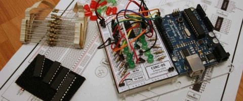
A breadboard is an essential tool for building and testing electronic circuits. It allows you to prototype circuits without having to solder components together. But before you can start building circuits, you need to understand how to properly layout and organize a breadboard. A well laid out breadboard will make your projects go together smoothly and efficiently.

In this guide, we will cover everything you need to know about laying out a breadboard, including:

  • What is a breadboard and how does it work?
  • Breadboard layout tips and best practices
  • Organizing components on a breadboard
  • Wiring methods for neat and orderly breadboards
  • Testing continuity on a breadboard
  • Common breadboard mistakes to avoid

Properly laying out your breadboard is a foundational skill for any electronics hobbyist or student. Let’s get started!

What is a Breadboard and How Does it Work?

Solderable Breadboard

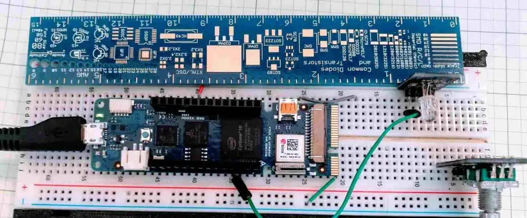
A breadboard, also known as a protoboard or prototyping board, is a construction base for building and testing electronic circuits. It consists of a plastic board with a grid of holes that are connected underneath in a specific pattern. The grid of holes allows you to insert components like resistors, capacitors, and integrated circuits. Underneath the board, metal clips connect certain holes together. This allows you to build circuits without having to solder components together.

Features of a Breadboard

  • Grid of holes for inserting components
  • Underlying metal clips connect holes in a certain pattern
  • Allows building circuits without soldering
  • Used for prototyping and testing circuits quickly
  • Reusable – components can be inserted and removed
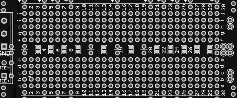
Power Rails

Breadboards have two long strips running vertically on the left and right side, often labeled red and blue. These are called the power rails. The holes in each power rail strip are connected horizontally to each other. This allows you to easily connect voltage and ground to your circuit by plugging wires into the rails. The red rail is commonly used for positive voltage (VCC) while the blue rail is used for ground (GND). However, you can use them for any two voltages required in your circuit.

Main Working Area

The main working area consists of short 5-hole rows split by a center gap, forming a rectangular grid. The holes in each 5-hole row are connected horizontally to each other. But there are breaks in between each row, columns across the center gap, and columns along the power rails. This pattern allows you to insert components and create a circuit by connecting rows with jumper wires without shorting paths together.

Breadboard Layout Tips and Best Practices

Laying out your breadboard properly will make building and testing circuits much easier. Here are some tips and best practices to follow:

  • Orient components across the center gap – Place positive pin/lead in one row, negative pin/lead in a row across the gap. This prevents short circuits.
  • Keep layout consistent from one section to the next – Maintain alignment and organization across the entire board.
  • Leave space between components – Don’t crowd parts together too tightly. Leave a hole or two between components.
  • Run wires cleanly along rows – Use jumpers to connect rows, not haphazard diagonal wires between holes.
  • Label rows used for signals – Identify inputs, outputs, control lines, etc using masking tape.
  • Use breadboard row numbering – Refer to row numbers when wiring up circuits from schematics.
  • Connect power and ground rails cleanly – Run a red wire to red rail, blue wire to blue rail. Avoid twisting wires.
  • Check for continuity and shorts – Verify connections are good and there are no shorts before powering up.

Following these breadboard layout guidelines will give you neat, orderly and properly functioning circuits.

Organizing Components on a Breadboard

Keeping your breadboard clearly organized goes hand-in-hand with proper layout. Here are some tips on organizing parts and wires on a breadboard:

Group Related Components

  • Keep all parts for individual sub-circuits grouped together in one section. For example, group all resistors and transistors for an amplifier circuit together.
  • Draw boxes on masking tape to define sections if needed.

Align ICs Properly

  • Position integrated circuits (ICs) across the center gap, with a leg on each side of the gap.
  • Align notches on ICs with the top and bottom power rail rows.

Orient polarized components properly

  • Position polarized caps and diodes with their positive and negative legs in different rows.

Cut jumper wires to length

  • Use wires only as long as necessary between connections. Cut excess wire lengths.

Label jumper wires

  • Use small pieces of masking tape to identify signals on jumper wires. For example, “Clock”, “Data”, “Reset”.

Organizing components properly on your breadboard will make your circuit much easier to assemble, troubleshoot and modify.

Wiring Methods for Neat and Orderly Breadboards

How you wire up your breadboard can greatly affect the orderliness and appearance of your project. Here are some techniques for neat and orderly breadboard wiring:

Run wires along rows

  • Run jumper wires along breadboard rows, not diagonally between random holes. This keeps everything straight and parallel.

Use different row paths for signal lines

  • Run different signal lines through different rows. If two signal lines overlap, cross them in an “X” pattern.

Insert wires into tidy rows

  • When inserting component leads or wires into the breadboard, align them into straight, tidy rows. Avoid haphazard insertion.

Secure components and wires

  • Use masking tape or other adhesive to secure IC bodies and jumper wires to keep them in place.

Avoid wire tangles

  • Be mindful of wire connections as you insert components into the board to avoid tangled masses of wire connections.

Cut wire lengths

  • Clip jumper wires to only necessary lengths between connections for tidiness.

Check alignments

  • Periodically check that components and wires are still aligned properly and securely as you build your circuit.

Following these tips as you assemble your breadboard will result in an orderly layout that looks neat and professional.

Testing Continuity on a Breadboard

Once you’ve completed your breadboard layout, it’s crucial to test for continuity to verify proper connections before powering up your circuit. Here is the process for testing continuity:

Visual Inspection

  • First visually inspect that components appear to be inserted into the appropriate rows and aligned properly. Verify wires are along rows.

Use a Multimeter

  • Set your multimeter to continuity check mode – this makes it beep when a connection is detected.

Check Each Wire and Connection

  • Touch the multimeter probes to both ends of each wire and component connection to ensure they are properly connected with continuity.

Verify Power and Ground

  • Check continuity from power and ground rails out to each part of your circuit that should connect to the supplies.

Look for Short Circuits

  • Probe different points in your circuit that should NOT be connected to see if shorts exist, indicated by unwanted continuity.

Fix Any Issues

  • If any defects are identified, fix miswirings, shorts, or poorly inserted components.

Only after you have visually inspected your layout and verified with multimeter tests that the circuit matches the schematic, should you connect power and begin functional testing. This will ensure basic wiring issues don’t damage components when power is first applied.

Common Breadboard Mistakes to Avoid

Even experienced electronics hobbyists make breadboarding mistakes now and then. Being aware of common errors will help you avoid them in your projects:Not Aligning ICs Properly

  • Be sure to align any integrated circuits across the center gap, following pinout diagrams.

Not Confirming Polarity of Polarized Parts

  • Diodes, LEDs, caps and more are polarized. Verify orientation!

Inserting Jumpers or Components Messily

  • Take care to align jumper wires along rows and neatly insert each component.

Connecting Incorrect Rows to Schematic

Failing to Identify Rows or Jumpers

  • Labeling rows and wires avoids confusion on complex boards.

Crowding Too Many Parts Together

  • Spread components out with space between parts for easier assembly and debugging.

Avoiding these common pitfalls will ensure your breadboard wiring is laid out properly and your circuit has the best chance of functioning correctly on the first try.

Conclusion

Bread Circuit Board

Laying out a breadboard properly is key to building and testing circuits successfully. By following breadboard layout best practices, neatly organizing parts, wiring intelligently, verifying connections, and avoiding mistakes, you can assemble functioning circuits in no time.

The gridded layout and lack of soldering allows flexible prototyping, but introduces challenges in layout that don’t exist for permanent PCBs. Carefully planning breadboard arrangements will give you a smooth electronics project workflow.

So grab your breadboard, multimeter, jumper wires and components and start creating your next electronics design using these breadboard tips!

FQA

What are the main parts of a breadboard?

The main parts of a breadboard are:

  • Power rails – Long vertical strips for connecting power and ground.
  • Binding posts – Terminals to connect external power to the rails.
  • Main grid area – Contains short 5-hole rows connected horizontally underneath to allow component and wire insertion.
  • Center gap – Splits the grid into two sections for separating circuits.

Why are breadboards designed with two separate halves?

The split grid design of breadboards, with a gap down the middle, is to prevent short circuits between two circuits or circuit elements that should not be connected. The gap provides isolation between the two grid halves.<h3>How should you arrange ICs on a breadboard?

Integrated circuits should straddle the center gap of the breadboard, with half the IC legs on one side of the gap and the other half on the opposite side. Align notches on the IC package with the top and bottom rails. This prevents shorting power and ground connections.

Why should you use short jumper wires between connections?

Excess long jumper wires can lead to tangled messy rats nests on a breadboard. Using the shortest wire possible between connections results in a cleaner layout. It also reduces noise pickup and voltage drops along wire lengths.

What is the best way to document and label a breadboard?

Use small pieces of masking tape to label rows used for important signals. Draw boxes on sections of the board used for separate circuits. Clearly label inputs, outputs and power connections. This makes the layout easy to understand and debug.

How to Design a Good Battery Management System (BMS) ?

Battery Thermal Management System

Introduction

A battery management system (BMS) is an electronic system that manages a rechargeable battery pack. Its main functions are to monitor the battery’s state, calculate secondary data, report that data, control its environment, authenticate and balance the individual cells and protect the battery. A good BMS is crucial for extracting maximum performance from a battery and ensuring its safe operation. When designing a BMS, the main considerations are:

  • Safety and protection features
  • Accurate monitoring and measurements
  • Effective balancing and optimization
  • Reliable performance and durability
  • Comprehensive data reporting
  • Flexible functionality and connectivity

This article provides a comprehensive guide on how to design an effective BMS, covering key factors like topology selection, hardware components, software algorithms, testing and more.

Topology Selection

The first step in designing a BMS is deciding on the topology or architecture. This influences factors like cost, complexity, scalability and capabilities. Common topologies include:

Centralized BMS

In a centralized topology, a single control board manages the entire pack.

Advantages:

  • Simple and low cost for small battery packs
  • Easier to program and debug

Disadvantages:

  • Doesn’t scale well for large battery packs
  • Single point of failure – if control board fails, whole BMS fails

Modular/Distributed BMS

Distributed BMS uses multiple linked control boards, each managing a section of the battery pack.

Advantages:

  • Highly scalable and flexible
  • No single point of failure
  • Supports large battery packs

Disadvantages:

  • More complex programming and debugging
  • Higher cost due to multiple boards

Master-Slave BMS

A master controller board oversees the entire pack while connected slave boards manage sections of the pack.

Advantages

  • Flexible and scalable like distributed topology
  • Centralized control through master board

Disadvantages

  • Added complexity of master-slave communication
  • Potential single point of failure at master

Choose a topology appropriate for your pack size, cost, complexity, and scalability needs.

Hardware Design

Battery Circuit Diagrams

The hardware components of a BMS can be divided into:

  • Control and measurement circuitry
  • Power electronics
  • Communication interfaces
  • Enclosure and structural elements

Careful selection of these elements is key to building a reliable and functional BMS.

Control and Measurement Circuitry

This includes the microcontroller and other circuits that monitor cell voltages, temperatures, etc. and run the BMS algorithms. Key factors are:

  • Microcontroller – Select one with adequate memory, processing power, peripherals (ADC, timers etc.) and operating voltage range. Popular options are ARM Cortex-M, PIC, AVR.
  • Cell monitoring – BMS needs accurate voltage and temperature monitoring of each cell. Choose components with necessary resolution, accuracy, and isolation.
  • Current/power monitoring – Shunt resistors, hall effect sensors or similar components used to measure pack current.
  • Other sensors – May include pressure, humidity, etc. depending on pack requirements.

Power Electronics

Power electronic components are required in active balancing and protection features:

  • Balancing – Bleed resistor, active balancing ICs or DC-DC converters used to match cell voltages.
  • Fuses/breakers – Protect pack from overcurrents.
  • MOSFETs – Control contactors or current flow.
  • Isolation – Isolators, opto-couplers and similar components provide voltage isolation.

Select parts rated for maximum pack voltage and current.

Communication Interfaces

Interfaces allow the BMS to communicate data and alerts:

  • External interfaces – CAN, LIN, RS232, Ethernet, etc. to communicate with other vehicular systems.
  • Cell interfaces – SPI, I2C etc. to connect with cell monitoring ICs.
  • Debugging interfaces – UART/JTAG for testing and programming during development.
  • Wireless interfaces – Bluetooth, WiFi or similar for configuring BMS parameters wirelessly.

Enclosure and Structural Elements

The BMS hardware needs to be securely mounted and protected. Enclosure selection factors:

  • Form factor, dimensions – rackmount or enclosure conforming to pack dimensions
  • Material – metal, high impact plastic etc.
  • Environmental rating – IP65, IP67 or higher for protection from dust and moisture
  • Connectors – high quality connectors for external wiring interfaces
  • Structural – mounting plates, braces and slots for PCBs and components
  • Thermal – heat spreading design, ventilation, cooling fan if high power

Software Design

Well designed software and algorithms are crucial for enabling the core functionality of a BMS. Key aspects include:

Cell Monitoring

  • Voltage measurement – ADC sampling, filtering, averaging to get stable values
  • Temperature measurement – sensing and cold junction compensation for thermocouples
  • State of charge estimation – voltage translation, coulomb counting models
  • State of health monitoring – capacity estimation, internal resistance tracking

Battery Protection

Safety critical protection features like:

  • Overvoltage/undervoltage protection
  • Overcurrent/short circuit protection
  • Overtemperature protection
  • Under and over SOC limits

This requires parameter thresholds, hysteresis factors, timing analysis and control logic.

Cell Balancing

Balancing algorithms to match cell voltages and states of charge:

  • Passive balancing – bleed overcharged cells
  • Active balancing – shuttle current between cells
  • Cell selectivity logic – which cells to balance and when

Thermal Management

  • Model cell/pack thermal behaviour
  • Temperature based control of cooling systems
  • Limit power during thermal faults

Diagnostics and Reporting

  • Status indicators, warnings and faults
  • Usage metrics – histograms, cycling, etc.
  • Expose internal data over communication interfaces
  • Data logging to support analytics and troubleshooting

Other Features

  • State machine, startup and shutdown control logic
  • Security against unauthorized access
  • Remote update capability over the air

Selecting the right algorithms and optimizing them is key to maximizing performance. Rigorously test edge cases.

Hardware Testing

Once the BMS hardware design is complete, it must go through rigorous testing to validate functionality and reliability.

Key testing activities include:

  • Unit testing of individual hardware components like sensors, power electronics, microcontroller modules etc. This verifies that each component works as per specifications before system integration.
  • Integration testing after assembling all components together. Validate all internal interfaces like sensor connections to microcontroller, communication between microcontroller and power electronics.
  • Functionality testing of all primary BMS functions – voltage, current and temperature sensing, balancing, contactor control, data logging etc. Map functionality to requirements.
  • Environmental testing by putting system under expected operating conditions – temperature, humidity, vibration, shock etc. Verify operation and durability.
  • Failure testing by simulating component failures – microcontroller faults, sensor bias or gain issues, contactor stuck closed or open etc. System should detect and handle failures gracefully.
  • Performance testing with different load conditions, cell configurations, balancing needs etc. Quantify metrics like balancing speed, controller utilization.
  • Long term reliability testing through prolonged continuous operation to uncover any lingering flaws.

Any issues discovered should lead to design revisions and another round of testing until hardware validation is complete.

Software Testing

Similar rigorous methodology must be followed when testing the BMS software and algorithms.

Key testing approaches include:

  • Unit testing – Validate each software module/function independently. Mock hardware interfaces and inputs.
  • Integration testing – Test interactions between software components.
  • Interface testing – Verify inputs from actual hardware components like sensors.
  • Automated testing – Write test scripts to exercise different code paths. Makes regression testing easier.
  • Fuzz testing – Provide randomized invalid/unexpected inputs to uncover corner case flaws.
  • Model based testing – Simulate battery model and operational conditions to test without actual cells.
  • Real world validation – Ultimately test BMS on actual cells/packs close to intended application.

Continuously execute above tests and address issues during development. Perform regression testing after every code change.

Safety Validation

Safety is paramount for any battery system. The BMS design needs independent validation to ensure it mitigates safety risks.

Key validation activities include:

  • Standards compliance – Verify BMS meets applicable equipment safety standards – UL1973, IEC 62619 etc.
  • Failure modes and effects analysis (FMEA) – A systematic analysis of potential failure modes in BMS and their effects on safety. Helps identify and mitigate high risk conditions.
  • Fault injection testing – Deliberately induce faults into BMS – controller crashes, sensor failures, erroneous data etc. – and validate failure handling.
  • Abusability testing – Test consequences of misuse – wrong wiring, incorrect settings, out of range inputs etc. BMS should gracefully handle errors.
  • Fire and smoke testing – Verify materials meet flammability standards. Check for smoke generation during thermal faults.
  • Environmental testing – Test effects of humidity, contamination, temperature extremes etc. on safety.
  • Security analysis – Validate protection against cyber attacks and unauthorized access.
  • Manual reviews – Experts should review schematics, software code, test results etc. and identify any gaps.
  • Certification – For commercial products, certification by accredited safety agencies adds credibility.

Remediate any identified safety issues and iterate until rigorous validation is achieved.

Configuration and Manufacturing

The last phases of BMS development involve optimizing it for production and deployment.

  • Version control – Maintain central repository of hardware designs, software code, documentation etc. and track changes.
  • Configuration management – Define part revisions, serial numbers, branding. Ensure traceability from components to finished product.
  • Manufacturing planning – Create drawings, BOM, assembly procedures, test specifications etc. for production. Plan supply chain logistics.
  • Production line testing – Validate sample units built on production line meet specifications through testing and QA.
  • Field configuration – Determine how to configure BMS parameters like cell counts, protection thresholds, balancing rates for each application.
  • Calibration – Define process to calibrate measurement accuracy – current sensor offsets, voltage scaling etc. – during production and in field.
  • Diagnostics – Add capabilities like data logging that assist in troubleshooting issues after installation.

With meticulous execution of the above steps, a safe, reliable, high performance BMS can be designed for battery systems.

FAQ

Here are some frequently asked questions about designing battery management systems:

Q: How do I choose between a centralized vs distributed BMS topology?

A: Centralized BMS is good for small to medium battery packs while distributed BMS is preferred for very large packs due to better scalability and lack of single point of failure. Also consider cost, complexity and troubleshooting needs.

Q: What are the most important safety features in a BMS?

A: Key safety features are overvoltage, undervoltage, overcurrent, overtemperature protections. These help prevent catastrophic battery failures. Also critical is failure handling – BMS should detect internal faults and transition to a safe state.

Q: What level of voltage and temperature measurement accuracy is needed in a BMS?

A: Ideal voltage measurement accuracy is at least +/-10mV to enable accurate state of charge estimation. Temperature sensors should have +/-1C accuracy or better for effective thermal monitoring.

Q: How much processing power does the BMS microcontroller need?

A: Microcontroller needs adequate memory and speed to run monitoring and safety algorithms while managing communication protocols. For a 1000 cell pack, Cortex M4 or higher is recommended.

Q: What communication interfaces should a BMS support?

A: CAN bus is commonly used to communicate with other vehicle systems. Additionally provide options like RS232, USB etc. for interfacing during development, testing and maintenance.

Top 15 Electronics Components Suppliers in the World

electronic components procurement

The electronics components industry is a massive global business that manufactures the parts and materials needed to build electronic systems and devices. From semiconductors to passives, connectors to electromechanical, here are the 15 largest electronics component suppliers in the world.

1. Samsung Electronics

Samsung is the worldโ€™s largest manufacturer of memory chips including DRAM and NAND flash memory. It is also a powerhouse in advanced displays and smartphones. Samsung is the number one semiconductor supplier in the world.

2. Intel Corporation

Intel FPGA Board
Intel FPGA Board
  • Headquarters: United States
  • 2019 revenue: $72 billion
  • Products: Microprocessors, chipsets, SSDs, Wi-Fi, modems

Intel is the leading manufacturer of PC and server microprocessors including CPUs and chipsets. It has led the transition of x86 architecture to multicore parallel processing for over a decade.

3. Taiwan Semiconductor (TSMC)

  • Headquarters: Taiwan
  • 2019 revenue: $34.6 billion
  • Products: Wafer foundry, integrated circuits

TSMC pioneered the dedicated silicon foundry model for IC fabrication. It manufactures chips for fabless companies using leading edge process nodes. The worldโ€™s largest silicon wafer fabrication plant.

4. SK Hynix

  • Headquarters: South Korea
  • 2019 revenue: $26.5 billion
  • Products: DRAM, NAND flash, SSDs

SK Hynix is a major memory semiconductor supplier engaged in the design and manufacture of DRAM and NAND flash memory chips. Also a leading supplier of wafer foundry services.

5. Broadcom

  • Headquarters: United States
  • 2019 revenue: $22.6 billion
  • Products: Semiconductors for wired, wireless communications

Broadcom is a leading designer, developer and supplier of RF, analog, digital and mixed signal integrated circuits for the wireless and broadband communication markets.

6. Qualcomm

  • Headquarters: United States
  • 2019 revenue: $24.2 billion
  • Products: Cellphone chipsets, modems

Qualcomm invents breakthrough technologies for the wireless industry. It is the worldโ€™s largest fabless semiconductor company supplying chips, software and services for mobile devices and wireless networks.

7. NVIDIA

NVIDIA is the leading manufacturer of graphics processors (GPUs) used in PCs, data centers, mobile devices and autonomous vehicles. It pioneered programmable shading and GPU computing.

8. Texas Instruments

  • Headquarters: United States
  • 2019 revenue: $14.4 billion
  • Products: Analog ICs, embedded processors

Texas Instruments is the worldโ€™s largest supplier of analog components and embedded processors. Its catalog includes tens of thousands of analog ICs covering amplifier, regulator, ADC/DAC, interface applications.

9. STMicroelectronics

  • Headquarters: Switzerland
  • 2019 revenue: $9.5 billion
  • Products: Automotive, industrial, personal electronics ICs

ST Microelectronics is an innovative global semiconductor leader that designs, develops, manufactures and markets a wide range of products for automotive, industrial and personal electronics applications.

10. Infineon Technologies

  • Headquarters: Germany
  • 2019 revenue: โ‚ฌ8.03 billion
  • Products: Automotive, industrial power, security microcontrollers

Infineon provides semiconductor solutions for automotive, industrial power control, power management, IoT, security and chip card applications. A leading supplier of power semiconductors globally.

11. ON Semiconductor

  • Headquarters: United States
  • 2019 revenue: $5.5 billion
  • Products: Image sensors, power semiconductors, analog ICs

ON Semiconductor offers a comprehensive portfolio of energy efficient power and signal management, logic, discrete and custom solutions for electronics system designers.

12. Raming Technology

  • Headquarters: Taiwan
  • 2019 revenue: $4 billion
  • Products: Optoelectronics, RF components

Raming is a global supplier of high quality optoelectronic and RF components including LEDs, laser diodes, BAW filters, amplifiers for consumer electronics, automotive, industrial, telecom applications.

13. NXP Semiconductors

  • Headquarters: Netherlands
  • 2019 revenue: $8.9 billion
  • Products: Automotive, security, networking processors

NXP Semiconductors provides high performance mixed signal and standard product solutions. It is a leader in automotive semiconductors, mobile, identification applications.

14. Renesas Electronics

  • Headquarters: Japan
  • 2019 revenue: $7.2 billion
  • Products: Microcontrollers, analog, power semiconductors

Renesas delivers trusted embedded design innovation for the automotive, industrial, home electronics, office automation and information communication technology markets.

15. Corning Inc.

  • Headquarters: United States
  • 2019 revenue: $3.5 billion
  • Products: Optical fiber, optical materials, ceramics

Corning is the world’s leading innovator and manufacturer of optical fiber, glass and ceramics used in communications networks, mobile consumer electronics, scientific and defense technologies.

Conclusion

Xilinx Artix 7
Xilinx Artix 7

This list covers the 15 largest global corporations involved in the supply of electronic components, semiconductors, interconnects, passives and other materials that enable modern electronics manufacturing. Their continued research, development and supply of critical components drives the exponential technological progress that shapes the electronics landscape.

Frequently Asked Questions

Q1. What are the major types of electronic components?

Major component types are:

  • Semiconductors – Diodes, transistors, ICs
  • Passives – Resistors, capacitors, inductors
  • Interconnects – Printed circuit boards, connectors
  • Electromechanical – Relays, switches, sensors
  • Displays – LCD, LED, OLED
  • Memory – RAM, ROM, Flash memory

Q2. What are the latest developments in electronic components?

Some latest developments are:

  • 5G communication ICs
  • Embedded machine learning ICs
  • Wide bandgap power semiconductors
  • Flexible and stretchable circuits
  • Silicon carbide and gallium nitride devices
  • Biometric sensors
  • High density memories

Q3. What are the key raw materials used to manufacture electronics components?

Key raw materials are:

  • Silicon
  • Copper
  • Aluminum
  • Gold
  • Tin
  • Tantalum
  • Palladium
  • Plastics and epoxies
  • Rare earth metals

Components also use chemicals like acids, gases, photoresists and dopants.

Q4. What are the environmental concerns around electronics manufacturing?

Some concerns are:

  • Chemical use and waste
  • High energy and water consumption
  • Air and water emissions
  • Recycling difficulties due to complex materials
  • Conflict mineral sourcing issues
  • Occupational health hazards

Strict environmental regulations guide electronics companies.

Q5. How can counterfeit electronics components be detected?

Detection techniques include:

  • Visual inspection of markings, packaging, materials
  • X-ray imaging to look inside components
  • Electrical parameter testing outside tolerance limits
  • Forensic chemical analysis for material confirmation
  • Microscopic examination for signs of remarking
  • Traceability documentation checking

Supply chain controls and testing helps mitigate counterfeit risks.

How is semiconductor manufactured?

manufacture semiconductor

Semiconductor manufacturing is the complex process of fabricating integrated circuits (ICs) on silicon wafers. It involves hundreds of precision steps to build transistor structures layer by layer to create the complex integrated circuits that power electronic devices.

Overview of semiconductor manufacturing process

The key steps in fabricating a semiconductor chip are:

  1. Wafer fabrication – Producing raw silicon wafers
  2. Wafer processingย – Building transistors and circuits on wafers
    • Oxidation – Growing insulating oxide layer
    • Photolithography – Transferring circuit pattern onto wafers
    • Etching – Removing selected areas of oxide layer
    • Ion implantation – Inserting impurity atoms into silicon
    • Deposition – Adding thin film material layers
    • Chemical mechanical planarization (CMP) – Smoothening wafer surfaces
  3. Device assembly – Dicing, packaging and interconnect
  4. Final testing – Verifying and grading ICs according to performance

Advanced semiconductor fabs utilize robotic automation and strict cleanroom environments for precision manufacturing. Let’s look at the key steps in detail.

Wafer fabrication

manufacture semiconductor

High purity semiconductor grade silicon is required as the starting material.

Silicon ingot growth

  • Ingots grown using Czochralski or Float zone methods to form large single crystal ingots.
  • Diameter up to 300mm. Grown as near-perfect monocrystalline material.

Wafer slicing

  • Ingots are sliced into discs of required thickness – around 0.7-1 mm.
  • Diamond saws used for slicing to prevent silicon contamination.
  • Waters used for washing, cooling and catching debris.

Wafer finishing

  • Sliced wafers polished mechanically and chemically to achieve mirror finish.
  • Processes wafer edges to prevent chipping.
  • Cleaning done to remove contaminants.

Wafer testing

  • Tests done for material defects like dislocations, oxygen content.
  • Checks wafer thickness uniformity, TTV, reflectivity, resistivity.
  • Sorts wafers into grades based on quality.

Wafer processing

The sliced silicon wafers undergo hundreds of fabrication steps to build the ICs on them.

Oxidation

Silicon wafers coated with silicon dioxide to provide electrical isolation.

  • Thermal oxidation done by heating wafers to 900-1200ยฐC in oxidizing ambient.
  • Process forms high quality SiO2 layer of controlled thickness.
  • Acts as diffusion mask, isolates devices, reduces surface defects.

Photolithography

Transfers the integrated circuit layout onto the wafers layer by layer. Critical step with high precision requirements.

Photoresist application

  • Light sensitive photoresist liquid applied on wafers by spin coating.
  • Forms uniform thickness resist film across wafer surface.

Exposure

  • Wafers exposed to high intensity UV light through lithography mask containing IC pattern.
  • Light causes chemical changes in exposed photoresist regions.

Development

  • Chemical treatment dissolves exposed resist regions, transfers mask pattern onto resist.
  • Hardened resist remains in unexposed areas, acting as etch mask.

Advanced lithography uses 193nm wavelength UV, immersion techniques to achieve features below 10nm.

Etching

Selectively removes areas not protected by photoresist to transfer pattern onto wafer surface.

Wet etching

  • Wafer immersed in liquid etchant that chemically attacks exposed areas.
  • Isotropic etch profiles due to etching in all directions.

Dry etching

-Uses reactive ion gases like CF4 for anistropic vertical etching.

  • Achieves high precision with reduced undercut.

Etch selectivity ensures desired film is removed without damaging underlying layers.

Ion implantation

  • Introduces dopant impurity atoms like boron, phosphorus into silicon wafer.
  • Done after lithography to selectively implant regions not masked.
  • Creates n-type and p-type regions required to form devices.

Key parameters

  • Dopant ion type
  • Implant energy – Controls depth of penetration
  • Dose – Number of implanted ions per cm2

Activation annealing done post implantation to incorporate dopants.

Deposition

Adds thin layers of insulating and conductive material on wafers through deposition techniques.

Oxidation – To grow oxide layers

Chemical vapor deposition (CVD)

  • Reacts gaseous sources to deposit films like polysilicon, silicon nitride.
  • Provides conformal high quality films with controllable thickness.

Physical vapor deposition (PVD)

  • Evaporates/sputters target material that condenses on wafers.
  • Used to deposit metals for interconnects – aluminum, copper.

Atomic layer deposition (ALD)

  • Deposits films one atomic layer at a time through sequential reactions.
  • Enables thin, conformal films of materials like high-k dielectrics.

Chemical mechanical planarization (CMP)

Flattens wafer surface throughout processing steps for subsequent lithography.

  • Chemical slurry reacts with surface material.
  • Mechanical buffing removes reacted material.
  • Achieves global planarization across the wafer.

These wafer processing steps repeated 20-30 times to build the IC layer by layer.

Device assembly

Completed wafers are diced into individual chips and assembled into packages.

Wafer dicing

  • Diamond saws cut along scribe lines to separate individual die.
  • Protection films prevent surface damage during dicing process.

Die inspection

  • Individual dies tested electrically for defects using test probes.
  • Defect mapping done to log exact failure locations.

Die attach

  • Functional dies bonded onto lead frames or package substrates using epoxy adhesives.

Wire bonding

  • Microscopically thin gold/aluminum wires connected between die bonding pads and package pins.
  • Provides electrical connectivity.

Encapsulation

  • Protective plastic molded over package.
  • Only interconnect leads left exposed.

Marking

  • Inked dots or text printed on package to identify company, device type, batch number.

Lead finish

  • Lead frames plated with solder for SMT assembly, tin for soldering.

Final testing

us semiconductor companies

Before shipping to customers, ICs undergo final tests.

Wafer probing

  • Wafers probed before dicing to identify defective die.
  • Minimizes packaging known bad parts.

Inline tests

  • Automatic testers verify devices at each assembly step – wafer sort, pre-capsulation, final test.

Burn-in

  • Devices stressed at high temperature over time to identify early life failures.

Functional testing

  • Detailed parametric and functional tests done on automatic test equipment (ATE).

Packaged devices graded based on performance across parameters like speed, power, leakage. Binned into grades.

Conclusion

In summary, semiconductor manufacturing utilizes sophisticated processes like photolithography, etching, doping, deposition to mass produce integrated circuits with transistors below 10 nanometers on 300mm silicon wafers. The complexity of the manufacturing process results in low yield and high fabrication costs. But it enables the exponential advancement of computing power over the decades based on Moore’s Law.

Frequently Asked Questions

Q1. What are the different types of semiconductor device packages?

Some common semiconductor packages are:

  • Plastic dual in-line package (PDIP)
  • Quad flat pack (QFP)
  • Pin grid array (PGA)
  • Ball grid array (BGA)
  • Ceramic chip carrier
  • Chip-scale package (CSP)
  • Multi-chip modules (MCM)

Packages connect the silicon die to the printed circuit board.

Q2. What are the key materials used in semiconductor fabrication?

Some key materials used are:

  • Silicon – For substrates and growth of oxide
  • Photoresists – Light sensitive polymers for lithography
  • Dopants – Boron, phosphorus, arsenic for implantation
  • Etchants – Acids, plasmas for etching films
  • Dielectrics – Silicon dioxide, silicon nitride films
  • Metals – Aluminum, copper for interconnects

High purity materials critical for defect reduction.

Q3. What are the main differences between nMOS and CMOS processes?

  • nMOS uses only n-channel devices while CMOS uses both nMOS and pMOS devices.
  • CMOS utilizes complementary design for logic gates.
  • CMOS has much lower static power dissipation than nMOS logic.
  • Additional photolithography steps required for pMOS wells in CMOS.
  • nMOS simpler process with higher performance but higher power.

Q4. What are some advanced lithography techniques for IC fabrication?

Some advanced techniques used are:

  • Immersion lithography – Water fills gap between lens & wafer
  • Double patterning – Divides dense patterns into multiple exposures
  • Extreme UV lithography – 13.5nm wavelength light source
  • Electron beam lithography – Direct electron beam exposure
  • Nanoimprint lithography – Physical deformation of resist

Q5. How is mask data prepared for photolithography?

The mask data preparation steps are:

  1. Circuit layout designed using CAD tools.
  2. Layout fracturing splits data into mask patterns.
  3. OPC (optical proximity correction) compensates for optical distortions.
  4. Mask pattern data exported to fabrication tools.
  5. Masks fabricated with high accuracy for lithography.

Precision masks are critical to print nanoscale node geometries.

Xilinx FPGAs: A Comprehensive Guide to Product Families, Grades, Applications, and Costs

Xilinx Versal FPGA

Introduction to Xilinx FPGAs

Field-Programmable Gate Arrays (FPGAs) have revolutionized the world of digital circuit design, offering unprecedented flexibility and performance. At the forefront of this technology stands Xilinx, a company renowned for its innovative FPGA solutions. Xilinx FPGAs have become integral components in various industries, from automotive and aerospace to telecommunications and data centers.

Xilinx, now a part of Advanced Micro Devices (AMD), has been a pioneer in the FPGA industry since its inception in 1984. The company’s FPGAs are known for their high performance, energy efficiency, and adaptability, making them ideal for a wide range of applications. Whether you’re developing cutting-edge AI algorithms, designing advanced communication systems, or creating high-performance computing solutions, Xilinx FPGAs offer the versatility and power to bring your ideas to life.

In this comprehensive guide, we’ll delve into the world of Xilinx FPGAs, exploring their product families, grades, applications, and costs. By the end of this article, you’ll have a thorough understanding of Xilinx’s FPGA offerings and how they can benefit your projects.

Xilinx FPGA Selection Tool
RAYPCB Engineering Tools
Xilinx (AMD) FPGA Product Families
Spartan-7 Series
Cost-optimized FPGAs for high-volume, cost-sensitive applications. Ideal for I/O expansion, motor control, and sensor fusion.
6K-102K Logic Cells Up to 400 I/Os 4.5Mb BRAM $10-$80 USD
Artix-7 Series
Lowest power 7 series FPGAs optimized for cost and power. Perfect for software-defined radio, machine vision, and industrial IoT.
12K-215K Logic Cells Up to 500 I/Os 13Mb BRAM 6.6Gb/s Transceivers $20-$150 USD
Artix UltraScale+
Next-gen cost-optimized FPGAs with enhanced DSP and connectivity. For edge computing and protocol bridging.
Up to 352K Logic Cells 16.3Gb/s Transceivers 24.2Mb BRAM $80-$300 USD
Kintex-7 Series
Best price-performance ratio. Optimized for wireless infrastructure, video broadcast, and data center applications.
65K-478K Logic Cells Up to 500 I/Os 34Mb BRAM 12.5Gb/s Transceivers $100-$800 USD
Kintex UltraScale+
High-performance with optimal price/performance/power. Ideal for 5G, machine learning, and video processing.
Up to 1.1M Logic Cells 32.75Gb/s Transceivers 76Mb BRAM 2,880 DSP Slices $200-$2,000 USD
Virtex-7 Series
Highest performance and capacity FPGAs for demanding applications. ASIC replacement and high-bandwidth systems.
Up to 2M Logic Cells 28.05Gb/s Transceivers 68Mb BRAM 3,600 DSP Slices $1,000-$10,000 USD
Virtex UltraScale+
Highest performance with 58G PAM4 transceivers. For 400G networking, aerospace, and high-end compute acceleration.
Up to 2.8M Logic Cells 58Gb/s PAM4 Transceivers 394Mb Memory 12,288 DSP Slices $2,000-$30,000+ USD
Zynq-7000 SoC
All Programmable SoC with dual ARM Cortex-A9 cores + FPGA fabric. Perfect for embedded vision and motor control.
28K-444K Logic Cells Dual ARM Cortex-A9 Up to 1GHz CPU $30-$500 USD
Zynq UltraScale+ MPSoC
Multi-processor SoC with quad ARM Cortex-A53, dual Cortex-R5, Mali GPU + FPGA. For automotive ADAS and AI inference.
Up to 930K Logic Cells Quad ARM Cortex-A53 Dual Cortex-R5 Mali-400 GPU $100-$2,500 USD
Versal Adaptive SoC
Next-gen adaptive platform with AI Engines, ARM processors, and adaptable hardware. Industry’s first ACAP architecture.
AI Engines (400 TOPS) Dual ARM Cortex-A72 112Gb/s Transceivers Integrated NoC $500-$15,000+ USD
๐Ÿ’ก Note on Pricing
Prices shown are estimated ranges for production quantities and may vary based on package, speed grade, and quantity. Contact distributors for accurate quotes.
FPGA Selection Wizard

Answer the questions below to get personalized FPGA recommendations for your design.

Compare FPGA Specifications
Application-Based FPGA Selection Guide
๐Ÿญ
Industrial IoT
Spartan-7, Artix-7
๐Ÿ“น
Video Processing
Kintex-7, Zynq-7000
๐Ÿ“ก
5G Wireless
Kintex US+, Zynq US+
๐Ÿš—
Automotive ADAS
Zynq UltraScale+
๐Ÿ–ฅ๏ธ
Data Center
Virtex US+, Alveo
โœˆ๏ธ
Aerospace
Kintex US+, Virtex US+
๐Ÿค–
AI/ML Inference
Versal AI, Zynq US+
๐Ÿ”ฌ
Medical Imaging
Kintex-7, Zynq-7000
๐ŸŽฎ
Consumer Electronics
Spartan-7, Artix-7
๐Ÿ”Œ
Motor Control
Spartan-7, Zynq-7000
๐Ÿ“Š
High-Freq Trading
Virtex US+, Alveo
๐Ÿ”’
Cryptography
Zynq US+, Versal
Application Details
FPGA Resource Estimator

Estimate FPGA resource requirements based on your design blocks.

RAYPCB Engineering Tools | Xilinx and AMD are trademarks of AMD Inc.

Xilinx FPGA Product Families

Xilinx offers a diverse range of FPGA product families, each designed to cater to specific performance, power, and cost requirements. Let’s explore the main Xilinx FPGA product families:

1. Spartan UltraScale+ FPGA

The Spartan UltraScale+ family is Xilinx’s cost-optimized FPGA solution, designed for high-volume applications that require performance and power efficiency.

Key features of Spartan UltraScale+ FPGAs:

  • Optimized for cost-sensitive markets
  • Built on 16nm FinFET+ process technology
  • Offers excellent performance-per-watt
  • Suitable for applications like industrial IoT, motor control, and entry-level video processing

2. Artix UltraScale+ FPGA

Artix UltraScale+ FPGAs provide a balance of high performance and low power consumption, making them ideal for applications that require compact form factors and energy efficiency.

Key features of Artix UltraScale+ FPGAs:

  • Built on 16nm FinFET+ process technology
  • Offers up to 64 GTH transceivers with speeds up to 16.3 Gb/s
  • Supports PCIe Gen3 and Gen4
  • Ideal for applications like software-defined radio, machine vision, and medical imaging

3. Kintex UltraScale+ FPGA

Xilinx Kintex fpga
Xilinx Kintex fpga

The Kintex UltraScale+ family is designed for applications that demand high performance and bandwidth while maintaining a balance with power efficiency.

Key features of Kintex UltraScale+ FPGAs:

  • Built on 16nm FinFET+ process technology
  • Offers up to 64 GTY transceivers with speeds up to 32.75 Gb/s
  • Supports PCIe Gen3 and Gen4
  • Suitable for applications like 5G wireless, data center acceleration, and high-performance computing

4. Virtex UltraScale+ FPGA

Virtex UltraScale+ FPGAs represent Xilinx’s highest-performance FPGA family, designed for the most demanding applications that require maximum throughput and processing power.

Key features of Virtex UltraScale+ FPGAs:

  • Built on 16nm FinFET+ process technology
  • Offers up to 128 GTY transceivers with speeds up to 32.75 Gb/s
  • Supports PCIe Gen3, Gen4, and Gen5
  • Ideal for applications like AI/ML acceleration, high-performance computing, and aerospace & defense

5. Zynq UltraScale+ MPSoC

Xilinx Zynq fpga
Xilinx Zynq fpga

The Zynq UltraScale+ MultiProcessor System-on-Chip (MPSoC) family combines the flexibility of FPGAs with the power of embedded processors, creating a versatile platform for a wide range of applications.

Key features of Zynq UltraScale+ MPSoCs:

  • Integrates Arm Cortex-A53 application processors and Cortex-R5 real-time processors
  • Includes Mali-400 MP2 GPU for graphics acceleration
  • Built on 16nm FinFET+ process technology
  • Suitable for applications like autonomous driving, industrial automation, and embedded vision

Read more about:

Grades of Xilinx FPGA

Xilinx offers FPGAs in various grades to meet the specific requirements of different industries and applications. These grades ensure that the FPGAs can operate reliably in diverse environments, from consumer electronics to harsh industrial settings and even space applications.

1. Automotive Grade FPGA

Automotive grade FPGAs are designed to meet the rigorous standards of the automotive industry, including extended temperature ranges, high reliability, and compliance with automotive safety standards.

(1) Artix-7 XA

The Artix-7 XA family offers a cost-effective solution for automotive applications that require high performance and low power consumption.

Key features of Artix-7 XA FPGAs:

  • AEC-Q100 qualified
  • Operating temperature range of -40ยฐC to +125ยฐC
  • Ideal for advanced driver assistance systems (ADAS) and infotainment systems

(2) Artix UltraScale+ XA

Artix UltraScale+ XA FPGAs provide higher performance and integration for automotive applications, built on the advanced 16nm process technology.

Key features of Artix UltraScale+ XA FPGAs:

  • AEC-Q100 qualified
  • Operating temperature range of -40ยฐC to +125ยฐC
  • Suitable for autonomous driving and advanced in-vehicle networking

(3) Spartan-7 XA

xilinx-spartan-7-fpga-1

The Spartan-7 XA family offers a cost-optimized solution for automotive applications that require modest performance and low power consumption.

Key features of Spartan-7 XA FPGAs:

  • AEC-Q100 qualified
  • Operating temperature range of -40ยฐC to +125ยฐC
  • Ideal for automotive body electronics and entry-level ADAS applications

2. Defense Grade FPGA

Defense grade FPGAs are designed to meet the stringent requirements of military and aerospace applications, including extended temperature ranges, radiation tolerance, and long-term reliability.

(1) Artix-7 XQ

Artix-7 XQ FPGAs offer a balance of performance and power efficiency for defense and aerospace applications.

Key features of Artix-7 XQ FPGAs:

  • MIL-STD-883 compliant
  • Extended temperature range of -55ยฐC to +125ยฐC
  • Suitable for software-defined radio and electronic warfare applications

(2) Kintex-7 XQ

Kintex-7 XQ FPGAs provide higher performance and capacity for defense applications that require increased processing power.

Key features of Kintex-7 XQ FPGAs:

  • MIL-STD-883 compliant
  • Extended temperature range of -55ยฐC to +125ยฐC
  • Ideal for radar systems and high-performance signal processing

(3) Kintex UltraScale+ XQ

Kintex UltraScale+ XQ FPGAs offer advanced performance and integration for defense applications, built on the 16nm process technology.

Key features of Kintex UltraScale+ XQ FPGAs:

  • MIL-STD-883 compliant
  • Extended temperature range of -55ยฐC to +125ยฐC
  • Suitable for advanced radar systems and high-bandwidth communications

(4) Virtex-7 XQ

Virtex-7 XQ FPGAs provide the highest performance and capacity in the 7 Series defense-grade lineup.

Key features of Virtex-7 XQ FPGAs:

  • MIL-STD-883 compliant
  • Extended temperature range of -55ยฐC to +125ยฐC
  • Ideal for complex signal processing and cryptography applications

(5) Virtex UltraScale+ XQ

Virtex UltraScale+ XQ FPGAs represent the pinnacle of defense-grade FPGA performance, offering unparalleled processing power and integration.

Key features of Virtex UltraScale+ XQ FPGAs:

  • MIL-STD-883 compliant
  • Extended temperature range of -55ยฐC to +125ยฐC
  • Suitable for advanced electronic warfare and AI-enabled defense systems

3. Space Grade

Space grade FPGAs are designed to operate in the harsh environment of space, offering radiation tolerance and reliability for satellite and space exploration applications.

(1) Kintex UltraScale XQR

The Kintex UltraScale XQR family provides high-performance, radiation-tolerant FPGAs for space applications.

Key features of Kintex UltraScale XQR FPGAs:

  • Radiation-tolerant design
  • Total Ionizing Dose (TID) tolerance of up to 100 krad(Si)
  • Single Event Upset (SEU) mitigation techniques
  • Suitable for satellite communications, Earth observation, and space exploration missions

Xilinx FPGA Development Boards

Xilinx offers a wide range of development boards to help engineers and researchers prototype and test their designs using Xilinx FPGAs. These boards provide a convenient platform for exploring the capabilities of Xilinx FPGAs and developing applications across various domains.

Some popular Xilinx FPGA development boards include:

  1. Alveo Accelerator Cards: Designed for data center acceleration, these cards feature high-performance Xilinx UltraScale+ FPGAs.
  2. Zynq UltraScale+ MPSoC ZCU104 Evaluation Kit: A versatile platform for evaluating Zynq UltraScale+ MPSoCs, ideal for embedded vision and industrial IoT applications.
  3. Artix-7 FPGA Development Board: A cost-effective board for prototyping designs using Artix-7 FPGAs, suitable for various applications.
  4. Kintex UltraScale FPGA KCU116 Evaluation Kit: A high-performance development platform for exploring Kintex UltraScale FPGAs, ideal for communications and signal processing applications.
  5. Virtex UltraScale+ VCU118 Evaluation Kit: A cutting-edge development board featuring Virtex UltraScale+ FPGAs, designed for high-end applications and research.

These development boards come with comprehensive software support, including Xilinx’s Vivado Design Suite and Vitis unified software platform, enabling developers to quickly prototype and optimize their FPGA designs.

Cost of Xilinx FPGAs

Xilinx FPGA distributor

The cost of Xilinx FPGAs varies widely depending on the product family, performance capabilities, and volume of purchase. Here’s a general overview of the cost ranges for different Xilinx FPGA families:

  1. Spartan Series: 10โˆ’10โˆ’100+
    • Lowest cost option, suitable for high-volume applications
    • Price varies based on logic capacity and features
  2. Artix Series: 50โˆ’50โˆ’500+
    • Mid-range option balancing cost and performance
    • Price depends on logic capacity, transceiver count, and other features
  3. Kintex Series: 500โˆ’500โˆ’5,000+
    • Higher-performance option with increased logic capacity and features
    • Price varies significantly based on specific model and capabilities
  4. Virtex Series: 2,000โˆ’2,000โˆ’20,000+
    • High-end FPGAs with maximum performance and features
    • Pricing reflects the advanced capabilities and large logic capacities
  5. Zynq UltraScale+ MPSoCs: 500โˆ’500โˆ’10,000+
    • Pricing depends on the specific model, processor cores, and FPGA resources
    • Higher-end models with more powerful processors and larger FPGA fabric command premium prices

It’s important to note that these price ranges are approximate and can vary based on factors such as:

  • Volume of purchase: Bulk orders often receive discounts
  • Distribution channel: Prices may differ between authorized distributors
  • Specific model and features: Within each family, prices vary based on exact specifications
  • Market conditions: Prices can fluctuate due to supply and demand dynamics

For precise pricing information, it’s best to contact Xilinx or authorized distributors directly. Additionally, consider the total cost of ownership, including development tools, support, and power consumption, when evaluating FPGA solutions for your project.

Xilinx FPGA Application Markets

Xilinx FPGAs find applications across a wide range of industries and markets, thanks to their flexibility, performance, and ability to adapt to evolving standards. Here are some key application markets for Xilinx FPGAs:

1. Telecommunications and Networking

Xilinx FPGAs play a crucial role in the telecommunications industry, particularly in the development and deployment of 5G networks. They are used in:

  • 5G base stations and remote radio heads
  • Network function virtualization (NFV)
  • Software-defined networking (SDN)
  • High-speed optical transport networks

2. Data Centers and Cloud Computing

In the rapidly evolving world of data centers, Xilinx FPGAs provide acceleration for various workloads:

  • AI and machine learning inference
  • Database acceleration
  • Video transcoding and streaming
  • Network acceleration and security

3. Automotive

The automotive industry leverages Xilinx FPGAs for advanced driver assistance systems (ADAS) and autonomous vehicles:

  • Sensor fusion and processing
  • Computer vision for object detection and recognition
  • In-vehicle networking and infotainment systems
  • Functional safety systems

4. Aerospace and Defense

Xilinx’s defense-grade FPGAs are widely used in aerospace and defense applications:

  • Radar and electronic warfare systems
  • Satellite communications
  • Secure communications and cryptography
  • Avionics and flight control systems

5. Industrial Automation and IoT

In the industrial sector, Xilinx FPGAs enable smart manufacturing and Industry 4.0 initiatives:

  • Industrial robotics and motion control
  • Machine vision and quality inspection
  • Industrial IoT gateways and edge computing
  • Predictive maintenance systems

6. Healthcare and Medical Devices

Xilinx FPGAs contribute to advancements in medical technology:

  • Medical imaging systems (MRI, CT, ultrasound)
  • Real-time patient monitoring devices
  • DNA sequencing and bioinformatics
  • Surgical robots and assistance systems

7. Broadcast and Pro A/V

The media and entertainment industry relies on Xilinx FPGAs for:

  • 4K/8K video processing and encoding
  • High-definition video switching and routing
  • Real-time graphics rendering
  • Virtual and augmented reality systems

8. Consumer Electronics

While not as prevalent as in other markets, Xilinx FPGAs find their way into high-end consumer products:

  • High-performance gaming systems
  • Digital cameras and camcorders
  • Smart home devices and IoT hubs
  • Audio processing equipment

9. Scientific Research and High-Performance Computing

Xilinx FPGAs are valuable tools in scientific research and high-performance computing:

  • Particle physics experiments (e.g., at CERN)
  • Climate modeling and weather forecasting
  • Financial modeling and high-frequency trading
  • Quantum computing research and development

The versatility of Xilinx FPGAs allows them to address the unique challenges of each of these markets, providing customizable, high-performance solutions that can adapt to changing requirements and standards.

Conclusion

Xilinx FPGAs represent a powerful and versatile technology that continues to shape the landscape of digital design across numerous industries. From the cost-effective Spartan series to the high-performance Virtex UltraScale+ family, Xilinx offers a comprehensive range of FPGA solutions to meet diverse application needs.

The various grades of Xilinx FPGAs, including automotive, defense, and space-grade options, ensure that these flexible devices can operate reliably in even the most demanding environments. With development boards and robust software tools, Xilinx provides a complete ecosystem for engineers and researchers to innovate and bring their ideas to life.

While the cost of Xilinx FPGAs can vary significantly depending on the specific model and features, the total value proposition extends beyond the initial price. The flexibility, performance, and long-term adaptability of FPGAs often result in reduced overall system costs and faster time-to-market for many applications.

The wide range of application markets for Xilinx FPGAs demonstrates their versatility and importance in driving technological innovation. From telecommunications and data centers to automotive and healthcare, Xilinx FPGAs are at the forefront of enabling new capabilities and improved performance across industries.

As we look to the future, the role of FPGAs is likely to become even more critical. With the increasing demand for AI and machine learning at the edge, the need for customizable, high-performance computing solutions will only grow. Xilinx, now part of AMD, is well-positioned to continue driving innovation in the FPGA space, offering solutions that meet the evolving needs of developers and industries worldwide.

What is Near Field Communication (NFC) ?

Near Field Communication or NFC refers to a short-range wireless connectivity technology that enables simple and secure communication between devices that are in close proximity. NFC offers capabilities like contactless transactions, data exchange, device pairing and proximity-based interactions.

In this comprehensive guide, we will cover the fundamentals of NFC technology, how it works, protocols, standards, device integration, security considerations, use cases and its evolution.

Introduction to NFC

NFC or Near Field Communication is a standards-based wireless connectivity technology that allows devices within a short range to exchange information securely.

Some key aspects of NFC:

  • Operates at 13.56 MHz frequency based on RFID standards
  • Offers data speeds from 106 kbps to 424 kbps
  • Supports communication distances up to 10 cm
  • Enables intuitive “tap” based interactions between devices
  • Secure two-way communication between endpoints
  • Low power consumption for battery-powered devices

NFC enables compelling use cases like:

  • Contactless transactions via payment cards and terminals
  • Quick pairing between smartphones, peripherals and IoT devices
  • Sharing contacts, media files, web links etc through a simple tap
  • Fetching information from smart posters, tags and stickers via proximity
  • Automated actions and access control by bringing devices close together

NFC complements broader connectivity technologies like WiFi and Bluetooth by adding a short-range, low-power interaction model. Next, we will take a technical look under the hood at how NFC systems function.

How NFC Wireless Communication Works

NFC is based on RFID or Radio Frequency IDentification standards and operates in the globally available 13.56 MHz ISM band. It leverages electromagnetic induction between two loop antennas located within each other’s near field for communication.

The major components involved are:

NFC Reader/Writer – Actively generates an RF field and can read from or write data to compatible devices. Examples are payment terminals, smartphone NFC adapters.

NFC Tag – Passive tag that modulates data to the reader by detuning the RF field. Tags contain data and an NFC antenna.

NFC Peer-to-Peer – Two NFC-capable devices can exchange data in peer-to-peer mode.

NFC Card Emulation – Payment cards simulate an NFC tag to transmit card data to readers.

The basic NFC communication flow is:

  1. The reader/initiator generates an unmodulated 13.56 MHz RF carrier field.
  2. The tag or peer device draws power from the RF field and communicates by load modulation.
  3. Data is transmitted between the endpoints using modulation like ASK or PSK encoding schemes.
  4. Bit rates of 106, 212 or 424 Kbps are supported for communication.

This near field working range limits NFC connections typically to around 10 cm or less. NFC transmissions are also inherently secure since the short range limits eavesdropping/interception risks. Next, we look at the protocols and data exchange mechanisms supported by NFC.

NFC Protocols and Data Exchange

NFC defines standardized mechanisms for communication session initialization and data exchange between two devices. The core protocols are:

NFC Logical Link Control Protocol (LLCP)

LLCP allows two NFC-enabled peer devices to communicate in both directions. LLCP sets up the logical data communication channel and provides a reliable, orderly data exchange between the peer devices.

Key capabilities offered by LLCP include:

  • Service discovery – discover available services on the peer
  • Symmetry – both devices can send and receive

-Segmentation and reassembly – large packets are split and recombined

  • Multiplexing – communicate over multiple data links
  • Error handling – ensure data integrity
  • Flow control – manage transmission speed

LLCP is required for Android Beam file transfer and NFC based WiFi setup between Android devices. It can transport any application protocol.

NFC Data Exchange Format (NDEF)

NDEF defines a common data format for NFC messages transmitted between devices. The NDEF specification determines:

  • Message encapsulation – how payload is packaged
  • Record typing – assign record types like text, URI, binary etc.

-security handling

  • extensibility to add new record types

NDEF ensures interoperability between sender and receiver devices by establishing a standard data representation. This allows easy peer-to-peer exchange of things like contacts, web URLs, configuration parameters etc. simply by tapping devices together.

In card emulation mode, payment or transit cards also use NDEF to encapsulate data transmitted to the reader.

NFC Record Type Definitions (RTD)

RTDs provide specifications for various standardized record types like smart posters, text, URIs, Bluetooth handover etc. This allows common handling of these record types across devices.

For example, the Smart Poster RTD allows an NFC phone to consistently identify and interpret data from any compliant smart poster tag. RTDs ensure interoperability across the ecosystem.

Together, these protocols provide the foundation for reliable, interoperable data exchange between NFC devices.

NFC Operating Modes

NFC endpoints can communicate using several different operating modes:

Reader/Writer Mode

In this mode, the NFC device reads data from or writes data into passive NFC tags and stickers. This allows tagging real world objects and embedding information.

Use cases like asset tracking, smart packaging, interactive signage and contactless payments leverage reader/writer mode.

Card Emulation Mode

Here the NFC device like a smartphone emulates an NFC tag to another reading device like a payment terminal. This allows payments, transit ticketing and access control using the phone instead of a card.

The phone loads payment, ticketing, access control credentials into its secure element and presents it just like a contactless card when in proximity.

Peer-to-Peer (P2P) Mode

In P2P mode, two NFC-capable devices can exchange data like contacts, media files, web links etc. Android Beam leverages P2P mode. WiFi handoff also uses NFC P2P to exchange credentials.

P2P mode enables quick tapping to pair and share data across NFC devices.

By supporting these modes of communication, NFC delivers a diverse set of applications for consumers and enterprises, which we will cover later.

NFC Frequency Bands and Data Rates

NFC systems operate in the globally available, license-free 13.56 MHz ISM band. This frequency is leveraged since most countries allow free usage of 13.56 MHz band for industrial, scientific and medical purposes.

Within this ISM band, NFC implementations can take one of three possible carrier frequency choices:

  • 13.553 to 13.567 MHz – Center frequency 13.56 MHz
  • 13.56605 to 13.56795 MHz – Center frequency 13.56 MHz
  • 13.824 to 14.224 MHz – Center frequency 13.56 MHz

NFC antennas and coils are tuned for high efficiency at the center frequencies. The three sub-band options within ISM allow regional flexibility.

In terms of link data rate, NFC supports:

  • 106 kbit/s – Based on ISO/IEC 18092 standard
  • 212 kbit/s – For passive communication mode
  • 424 kbit/s – High data rate, active communication mode

Higher rates allow exchange of more data when devices are tapped together. 424 kbps is fast enough for quick small file or web page sharing between phones or computers using NFC.

NFC Standards

NFC technology has been standardized in multiple stages by standards bodies like:

ISO – International Organization for Standardization

IEC – International Electrotechnical Commission

ETSI – European Telecommunications Standards Institute

ECMA – European association for standardizing ICT and consumer electronics

NFC Forum – Standards body managing NFC specifications

Here is an evolution of key NFC standards:

  • ISO/IEC 18092 – Published 2004, defined modulation schemes and data transport
  • ISO/IEC 21481 – Published 2005, defined NFC interface and protocol
  • ECMA-340 – Published 2006, defined NFC peer-to-peer standards
  • ECMA-352 – Published 2008, defined NDEF data format
  • ISO/IEC 22536 – Published 2011, harmonized former standards
  • NFC Forum Specifications – Define implementation, use cases, testing

These standards ensure interoperability between NFC devices from different manufacturers. Let’s next look at the typical architecture for NFC controller chips and antennas.

NFC Hardware Architecture

The key hardware needed on a device for NFC functionality includes:

NFC Controller

This chip manages the wireless connectivity, communication protocols and data exchange with other NFC endpoints. It modulates and demodulates transmitted data.

Most NFC controllers integrate a secure element hardware block that stores payment or other sensitive credentials in a tamper-resistant manner.

Some example NFC controllers are:

  • NXP PN544 – Popular NFC controller used in many smartphones
  • NXP PN548 – High performance controller with integrated secure element
  • ST ST21NFC – NFC controller chip by STMicroelectronics

NFC Antenna

The NFC antenna is tuned to the 13.56 MHz frequency and allows the device to transmit and receive NFC signals. It is designed to offer good coupling with other NFC antennas that come in proximity.

NFC antennas typically consist of a copper coil etched onto a printed circuit board assembly. Multiple coil turns are used with 1nH typical inductance. Matching is done with capacitors.

Host Processor Interface

The NFC controller communicates with the main application processor of the device over standard interfaces like SPI, I2C, UART, USB. Software stacks use these interfaces.

NFC Power Management

Switches, regulators and amplifiers provide stable power supply to the NFC chips derived from the system battery voltage.

The controller, antenna and associated interfaces come together into an integrated NFC hardware module packaged as a single chip or PCB assembly for integration into the device.

Software Architecture

Here are some key components of the NFC software stack:

Host API – Allows applications to leverage and control NFC hardware capabilities

NFC Middleware – Manages interaction between applications, secure elements and hardware

Device Firmware – Low level firmware like RF analog control and digital protocol stack

Upper Layer Protocols – Software for protocols like LLCP, P2P, SNEP

Payment/Access Control Apps – Software for emulating transit cards, access cards

Peer-to-Peer Apps – Program logic for use cases like file sharing

Tag Reading Apps – Code to read, write and emulate NFC tags

On Android, the NFC software stack is implemented via Android’s NFC HAL (Hardware Abstraction Layer) and utilizes the NFC Forum Logical Link Control Protocol (LLCP) for peer-to-peer communication.

Apple implements similar software architecture within its CoreNFC frameworks introduced in iOS 11.

The firmware and software together orchestrate NFC operations, protocol handling, secure data exchange and use case management.

NFC Integration Into Devices

Here are some guidelines and considerations when integrating NFC hardware into a device:

  • Select NFC controller and antenna that supports target read range, power budgets
  • Ensure NFC module placement allows space for antenna and minimizes interference
  • Route signals from controller to host processor using robust interfaces like I2C
  • Provide sufficient decoupling and power supply stability to NFC module
  • Utilize shielding, ferrite sheets to limit interference from other subsystems
  • Over-the-air testing to validate read range, data speeds, accuracy
  • Test NFC performance in final device enclosure, with batteries, displays
  • Validation testing with representative NFC tags and reader devices

With careful integration, antenna tuning and testing, optimal NFC performance can be delivered within the device.

NFC Security Considerations

NFC offers simplified connectivity between devices, however it is important to keep security in mind:

Data Exchange

  • NFC’s short range limits potential for remote eavesdropping and man-in-the-middle attacks.
  • Encryption can be implemented for NDEF and application level data security.

Device Pairing

  • Visually confirm identity of the peer device being paired for consent.

Tags and Stickers

  • Avoid unexpectedly downloading or opening unverified content from unknown smart tags.

Relay Attacks

  • Guard against Attempts to relay or extend unauthorized NFC scans beyond immediate vicinity.

Transaction Verification

  • Double check transaction details on device screen before approving contactless payments.

Secure Element

  • Use hardware backed secure element for storage of payment credentials and keys.

By following device best practices and user awareness, NFC can be implemented securely across applications.

Applications and Use Cases

nfc manufacturer

Some major applications leveraging NFC technology include:

1. Contactless Payments

NFC enables card emulation mode on phones allowing users to tap to pay at POS terminals – fast, convenient and secure.

Contactless transactions under a certain value threshold often do not even need additional authentication. Major payment networks like Visa, Mastercard, American Express and Discover support NFC payments.

2. Transit Ticketing

NFC offers a convenient contactless ticketing solution for public transport. Riders simply tap their phone or ticket on bus validators for seamless access. Solution minimizes ticket lines.

Transit agencies save on issuing and managing disposable cards. Most major transport systems globally support NFC ticketing.

3. Access Control

NFC access cards for secure door entry can be replaced with an NFC enabled phone. Employees just tap their phone to enter secured office doors, data centers etc.

Easy issuance, revocation of digital credentials on the phone compared to plastic cards.

4. Device Pairing

Android Beam, Apple Wallet leverage NFC’s peer-to-peer mode to quickly transfer data like contacts, web URLs, documents etc. by tapping devices.

Tap can also be used to connect or configure peripherals like headphones, printers and speakers.

5. Information Sharing

Smart posters, tags and stickers with embedded NFC tags allow businesses to share information with a simple tap of the phone.

Can be used for interactive advertising, sharing menus, product info, schedules, in-store navigation etc.

6. Gaming Interactions

NFC enables interactive board games, playing cards and collectible toys by adding a digital dimension via the phone.

7. Automotive Use Cases

NFC can enable vehicle features like keyless entry and start, personalized dashboard profiles, garage door opening, parking payments etc.

8. Industrial Applications

NFC is also gaining adoption in industries to track assets, for equipment maintenance, factory automation, lab instrument management and other uses leveraging proximity based interactions and data exchange.

These examples illustrate the versatile applicability of NFC technology across consumer and enterprise segments.

The Future of NFC Technology

NFC has become firmly established over the past decade as a ubiquitous proximity wireless communication technology. Here are some trends shaping NFC’s future roadmap:

Increased Adoption in Smartphones – A growing number of smartphones now incorporate NFC allowing large addressable user base for applications.

IoT Connectivity – NFC offers easy pairing between IoT devices and homeowners’ smartphones to set up and manage appliances, smart home systems.

Advancing NFC Standards – Standards like NFC-V for vehicle integration and NFC-F for high data rate are emerging for new use cases.

NFC for Digital Key Sharing – Smart door locks and key cabinets are leveraging NFC to securely share digital keys using people’s phones.

Stronger Security – Advancing secure element, tokenization and biometric authentication technologies reinforce security of NFC payments and access control.

New Form Factors – Embedding NFC into more wearables, hearables, tablets and compute devices expands capabilities.

Innovation in Antennas – NFC performance is improving through integration, advanced antenna topologies like using magnetic induction.

NFC will continue evolving alongside smartphones and IoT endpoints to deliver more intuitive, convenient and secure interactions between people, devices and environments.

Conclusion

nfc-stickers

This brings us to the end of this comprehensive guide to NFC technology. We discussed how NFC systems function using inductive coupling, the communication mechanisms and protocols, integration considerations, security, applications across segments and the role of advancing standards.

NFC delivers a compelling blend of convenience, versatility and security to enable natural interactions using mobile devices. With applications from payments, transportation to interactive gaming and industrial automation, NFC adoption will continue growing as more smart objects populate our environment.

FAQs (Frequently Asked Questions)

How is NFC different from other wireless tech like RFID, Bluetooth and WiFi?

NFC offers very short range (touch-based), operates at 13.56MHz with low power consumption ideal for battery devices, and supports peer-to-peer mode.

What is the typical read range offered by NFC?

Practical NFC working distance is typically under 10cm. The proximity allows intuitive usage while providing inherent security against remote attacks.

Does NFC require pairing between devices before working?

NFC does not require traditional pairing and can securely exchange data between devices with just a tap without prior setup.

What data rates does NFC support?

NFC offers data rates ranging from 106 kbps to 424 kbps depending on implementation which is adequate for small data transactions.

What are some examples of NFC enabled devices?

Most modern smartphones, tablets, wearables, wireless headsets, smart home devices, retail terminals incorporate NFC.

What is an Arduino:Types, Projects and Applications ?

Introduction to Arduino

Arduino is an open-source electronics platform based on easy-to-use hardware and software. Arduinos make it simple for hobbyists and professionals to develop interactive electronics projects.

The key aspects of Arduino are:

  • Open-source – Hardware and software are open for anyone to use and modify.
  • Easy to use – The Arduino IDE and wiring interfaces abstract away complexity for beginners.
  • Flexible – Arduino boards can interface with a wide range of sensors, displays, motors, and other electronic components.
  • Inexpensive – The affordable boards make Arduino accessible for makers, students, and developers.
  • Cross-platform – Arduino software runs on Windows, Mac, Linux and cloud platforms.

Arduino has become the most popular open-source electronics platform, allowing millions of users to create interactive devices. Let’s examine Arduino boards, software, projects and applications in more detail.

Arduino Board Types

There are many types of Arduino boards available to meet different application needs. Here are some of the most common official Arduino board families:

Arduino Uno

The Arduino Uno is the classic entry-level Arduino board. It provides everything needed to start developing simple Arduino projects. Key features include:

  • Microcontroller: ATmega328P
  • Operating Voltage: 5V
  • I/O Pins: 14 Digital, 6 Analog
  • Flash Memory: 32 KB
  • Clock Speed: 16 MHz

With abundant tutorials and examples, the beginner-friendly Uno is the ideal starting point into Arduino.

Arduino Mega

The Arduino Mega2560 upgrades to a more powerful microcontroller chip and extensive I/O capabilities:

  • Microcontroller: ATmega2560
  • Operating Voltage: 5V
  • Digital I/O Pins: 54
  • Analog Input Pins: 16
  • Flash Memory: 256 KB
  • Clock Speed: 16 MHz

The Mega2560 is well suited for more complex projects requiring additional memory, processing power, and I/O lines.

Arduino Nano

The Arduino Nano packs the power of the Uno into a compact surface mount board:

  • Microcontroller: ATmega328P
  • Operating Voltage: 5V
  • Digital I/O Pins: 14
  • Analog Input Pins: 8
  • Flash Memory: 32 KB
  • Clock Speed: 16 MHz

With its small size, breadboard-friendly design, and abundance of I/O, the Nano is ideal for dense circuit prototyping.

Arduino Leonardo

The Arduino Leonardo differs by employing an ATmega32U4 microcontroller with built-in USB communication:

  • Microcontroller: ATmega32U4
  • Operating Voltage: 5V
  • Digital I/O Pins: 20
  • Analog Input Pins: 12
  • Flash Memory: 32 KB
  • Clock Speed: 16 MHz

The Leonardo can appear as a standard USB mouse or keyboard, facilitating HID projects.

Arduino MKR Family

The MKR boards offer compact, low power WiFi and cellular connectivity:

  • Microcontroller: ATSAMD21 Cortex-M0+
  • Operating Voltage: 3.3V
  • Digital I/O Pins: 8-12
  • Analog Input Pins: 6-8
  • Flash Memory: 256-512 KB
  • Connectivity: WiFi, GSM, LoRa

Choose an MKR board for IoT and wireless communication projects.

There are many other specialty Arduino boards like the MKR Vidor 4000 FPGA, ESplora with built-in sensors, and Portenta H7 with dual cores. This highlights the diversity of Arduino hardware.

Arduino Software

A key aspect of Arduino is its easy-to-use open source software. The Arduino IDE provides everything needed to program the boards in simple C/C++ based scripts.

The Arduino software includes:

  • Text editor for writing code
  • Compiler to build sketches
  • Uploader for installing sketches to an Arduino
  • Serially monitor Arduino communications
  • Libraries and examples to simplify coding

The flow involves:

  1. Writing a sketch using Arduino functions and libraries
  2. Compiling the sketch into executable code
  3. Uploading the hex file to the Arduino’s microcontroller

No advanced coding or hardware configuration is required. Arduino provides a seamless platform for programming interactive electronics projects.

Arduino Projects

Arduino’s versatility enables beginners to experts to create a huge variety of projects. Some examples include:

Basic Input/Output

  • LED light patterns
  • Reading switches and buttons
  • Driving motors, buzzers, and relays
  • Displaying text and shapes on LCDs

These simple but engaging projects teach Arduino I/O control.

Sensors

  • Motion detection with PIR sensors
  • Measuring temperature, humidity and gases
  • Detecting light levels with photoresistors
  • Capturing sound with a microphone
  • Ultrasonic and infrared distance ranging

Arduino is commonly used for sensor interfacing and data acquisition.

Robotics

  • Autonomous robot cars sensing the environment
  • Robotic arms with servos
  • Self-balancing robots
  • Swarm robots
  • Hexapod walking robots

Arduino provides an accessible brain for powering robots.

IoT and Wireless

  • Home automation with Bluetooth/WiFi
  • Weather stations sending data
  • Location trackers with GPS
  • Transmitting sensor telemetry
  • Smart agriculture monitoring

Arduino enables a range of wireless IoT edge devices.

Wearables

  • Fitness and health trackers
  • Smart watches
  • Virtual reality/augmented reality gear
  • Fashion tech
  • Assistive technology

Arduino can create interactive wearable electronics projects.

The applications are endless – if you can think of an electronics project, an Arduino can probably bring it to life!

Arduino Project Design Process

A structured development process helps ensure success as you design your Arduino project:

1. Define Objectives

  • What are the goals of your project? Desired functionality?

2. Flowchart Concepts

  • Diagram the logical flow and capabilities.

3. Select Components

  • Choose which Arduino board, sensors, displays and other components are needed.

4. Prototype the Circuit

  • Build the circuit on a breadboard and test functionality.

5. Write the Code

  • Program the Arduino to operate your circuit and application.

6. Troubleshoot and Refine

  • Fix issues, improve performance through an iterative process.

7. Construct Permanent Project

  • Solder your circuit and integrate into an enclosure or finished project.

This systematic approach will produce robust, high-quality Arduino projects.

Arduino Project Enclosure

arduino FPGA PCBA
arduino FPGA PCBA

For building permanent Arduino devices beyond a breadboard prototype, you need to integrate your project into an enclosure. Some options include:

  • Plastic boxes – Common for small projects, provides protection.
  • 3D printed cases – Design fully customized housings.
  • Laser cut enclosures – Stylish acrylic or wood cases.
  • Aluminum extrusion frames – An open modular support skeleton.
  • Machined enclosures – For metal housings with complex features.
  • Textile crafts – Knitted, sewn, or woven integrateion.
  • Portable batteries – Self-contained power for mobile projects.

Choose enclosures suited to your project’s mechanical, aesthetic, and functional requirements.

Applications of Arduino

Due to its versatility, there are limitless applications for Arduino across industries:

Education

Arduino provides an excellent hands-on platform for learning about electronics and programming in engineering, computer science, robotics, and physics courses. Arduino curriculum brings theoretical concepts to life.

Industrial Automation

For automation applications, Arduino can monitor sensors, valves, motors, process variables, and manufacturing lines. Arduino offers a low-cost programmable control platform.

Science Experiments

Arduino is valued by scientists for data acquisition and experimental controls. Arduino systems can automate experiments and record results.

Home Automation

In home automation, Arduino boards can integrate appliances, lighting, climate, security, pet care, and media systems into an intelligent connected home.

Audio Effects

For musicians, Arduino enables innovative synth pedals and audio effects like delays, distortions, loopers, and specialized real-time audio processing.

Assistive Technology

For adaptive needs, Arduino can interface with switches, wheelchairs, speaking aids, alternate input devices, alarms, and environmental controls.

Internet of Things

Arduino boards form the core of many networked monitoring and control systems with wireless connectivity to the cloud.

Wearable Technology

On wearables, Arduino provides a tiny programmable computer to make clothing and accessories interactive with sensors and LEDs.

From lab instruments to interactive art, Arduino serves limitless applications where an affordable, custom microcontroller system is needed.

Arduino Alternatives

While extremely popular, Arduino has inspired many other open-source hardware platforms. Some popular alternatives include:

  • Raspberry Pi – Low-cost single board computers running Linux. More power for applications like machine learning, computer vision, and network servers.
  • ESP32 – Microcontrollers with built-in WiFi and Bluetooth. For IoT and wireless products.
  • BeagleBoards – Open-source development boards with more processing performance for advanced applications.
  • SparkFun Inventor’s Kits – Curated electronics component kits teaching technology fundamentals.
  • STM32 – ARM Cortex MCUs with extensive I/O options and networking support.
  • PICAXE – All-in-one microcontroller boards focused on education.

Each platform has unique capabilities for different use cases. Arduino remains the most beginner-friendly choice.

Conclusion

In summary, Arduino provides an accessible open-source ecosystem for interactive electronics projects. Arduino boards offer an inexpensive microcontroller foundation with easy-to-use software. This empowers makers, students, researchers, and engineers to build innovative devices for just about any application. Arduino will continue fueling the creativity of the open-source hardware community for years to come.

Frequently Asked Questions

What are the main benefits of using Arduino vs. other microcontrollers?

The main advantages are beginner-friendly hardware, simplified programming, extensive documentation and examples, and low cost boards to get started.

What are some tips for starting out with Arduino?

Start with simple circuits to learn fundamentals. Seek example projects similar to your application. Use libraries when possible. Seek help from the large Arduino community.

Which sensors are most commonly used with Arduino?

Some of the most popular sensors are ultrasonic, accelerometer, gyroscope, magnetometer, temperature, force, capacitive touch, infrared, humidity, and gas sensors.

Can Arduino be used for advanced robotics?

Yes, Arduino can perform complex control tasks with the help of add-on motor controllers and advanced sensor systems. More powerful Arduino boards provide needed performance.

What is a good next step after learning Arduino basics?

Moving to alternative microcontroller platforms like Raspberry Pi or ESP32 allows creating more advanced IoT, network, and machine learning driven systems.

Full Introduction about Fr4 Dielectric Constant

PTFE Dielectric Constant

What is the Dielectric Constant?

The dielectric constant (Dk) is a property of insulator materials that describes how readily the material can transmit an electric field. It is defined as the ratio of the permittivity of the material to the permittivity of free space. A higher dielectric constant indicates more concentration of electric flux for a given applied voltage.

For printed circuit boards, the Dk of the substrate laminate materials directly impacts key parameters like impedance, capacitance, and propagation delay which influence signal integrity, EMI control, and many other aspects of circuit performance. As such, having a solid understanding of PCB dielectric properties is important for electrical engineers.

In this comprehensive guide, weโ€™ll cover everything you need to know about the FR4 dielectric constant specifically, including its meaning, typical values, impact on circuit design, how it varies based on composition, frequency, humidity, temperature, and more. Letโ€™s get started!

What is FR4 Material?

FR4 is the generic designation for the most common type of fiberglass-reinforced epoxy laminate material used as the substrate for rigid printed circuit boards. Some key attributes of FR4 include:

  • Glass fabric base material impregnated with flame-retardant epoxy resin
  • Available in wide range of thicknesses, typically from 0.4mm to 6mm
  • Composite construction provides mechanical strength and stability
  • Low cost, widely available, and well characterized for PCB fabrication
  • Used in vast majority of rigid PCB applications across consumer and industrial electronics

The FR4 designation comes from the flame-retardant treatment incorporated in the epoxy resin system. This gives the material enhanced fire resistance properties important for safe electronics assembly.

Multiple fabricators worldwide produce FR4 material in various grades under numerous trade names. But the performance is typically comparable for most general circuit board applications.

Typical FR4 Dielectric Constant

The dielectric constant of basic FR4 laminate materials commonly falls between 3.9 and 4.8 across frequencies up to around 1 GHz. Some examples include:

  • Isola FR408 HR – 3.9 to 4.4 over 1 MHz to 10 GHz
  • Nelco N4000-13 – 4.4 at 1 MHz falling to 4.1 at 1 GHz
  • Arlon CLTE – 4.7 over 1 MHz to 1 GHz
  • Taconic TLY – 4.6 over 100 MHz to 1 GHz

So in summary, assuming a Dk of 4.2-4.4 is reasonable for baseline budgetary FR4 dielectric assumptions up to GHz frequencies.

Of course, specialized FR4 blends are available from vendors with Dk values above and below the norm to meet particular requirements. Always check manufacturer data sheets for guaranteed properties.

Impact of Dielectric Constant on PCBs

The FR4 dielectric constant directly influences key electrical parameters that must be considered during circuit board layout and optimization. Some of the major interrelated impacts include:

Impedance

For a given PCB trace width and height over the ground plane, a higher Dk allows a higher characteristic impedance to be achieved. This impedance matching is vital for signal integrity.

Capacitance

A higher Dk leads to increased parasitic capacitance between conductors as greater electric flux can be stored. This must be considered for maintaining desired frequency response.

Propagation Delay

Signals propagate more slowly in higher Dk materials, increasing delay and flight times through traces which can limit high-speed performance.

Crosstalk

Faster signal edge rates coupled with higher Dk can increase crosstalk coupling to nearby traces which may require wider spacing.

Loss Tangent

Materials with higher Dk often have higher loss tangents, contributing more signal loss due to dielectric absorption.

EMI Susceptibility

Higher Dk materials concentrate more electrical flux, increasing susceptibility to external EMI interference.

Via Performance

With higher Dk, vias exhibit increased capacitive discontinuities, negatively impacting signal transmission through layer transitions.

In summary, the FR4 Dk impacts impedance control, propagation speed, parasitic capacitance, signal loss, EMI immunity, and more. Accounting for these effects is key during circuit optimization.

FR4 Dielectric Constant Variation

Itโ€™s important to understand that the FR4 dielectric constant is not a fixed value – it can vary based on several factors:

Resin Composition

The precise epoxy resin system used in the FR4 formulation impacts the dielectric constant. Values may differ slightly between various material suppliers.

Filler Composition

Dielectric properties change based on the filler content in the epoxy resin. Higher filler percentages generally increase the composite Dk.

Frequency

Dk decreases gradually with rising frequency due to polarizability effects. A 10-20% reduction over 1 MHz to 10 GHz is typical.

Fiberglass Weave

The weave pattern of the glass fabric in the laminate construction can create minor anisotropies in Dk.

Moisture Absorption

Absorbed moisture significantly increases Dk as water has a very high dielectric constant. This is a major concern.

Temperature

Dk exhibits a negative temperature coefficient, decreasing linearly with rising temperature due to increased molecular motion.

Lamina Thickness

Varying the number and thickness of laminate sheets changes the composite Dk based on the ratio of glass, resin, and air.

Copper Thickness

Since copper has a lower Dk than FR4, increasing copper thickness slightly lowers the overall composite Dk.

Manufacturing Tolerances

accepts. Slight Dk variations are possible in practice due to process variability.

Understanding these sources of variation allows designers to account for possible effects on critical parameters like impedance based on environmental exposure or production variance.

Controlling FR4 Dielectric Constant

fr4-dielectric-constant

To obtain a target dielectric constant, material suppliers can tailor the resin chemistry and filler composition. Some methods include:

  • Adjusting epoxy to phenolic resin ratios
  • Using brominated flame retardants to increase Dk
  • Incorporating high-Dk ceramic filler particles
  • Changing glass fabric weaves and density
  • Maximizing glass content for higher Dk

Tighter controls on lamination parameters like pressure and temperature also improve consistency. Engineers should select suppliers capable of providing guaranteed dielectric properties suitable for the application.

Low Dk and High Dk FR4 Materials

While standard FR4 materials for general use have a Dk around 4.2-4.6, engineered versions are available with dielectric constants above and below the norm.

Low Dk FR4

Some applications require lower dielectric constants. Properties down to Dk 3.0 can be achieved by:

  • Reducing glass fabric content in the composite
  • Using epoxy resin systems with lower polarizability
  • Tuning filler particle shapes and concentrations
  • Incorporating air voids into the laminate

High Dk FR4

For higher Dk values up to 6.0, manufacturers use tactics like:

  • Increasing glass fabric content
  • Employing non-brominated flame retardants
  • Adding high-Dk ceramic particles
  • Reducing resin flow for more air voids
  • Balancing resin viscosity and curing

Low Dk improves signal speed, while high Dk increases capacitance and impedance.

Dielectric Constant Testing

pcb dielectric constant

To validate that FR4 materials meet target Dk specs, standards-based qualification testing is used:

  • IPC-TM-650 – Test methods for printed boards
  • IPC-4103 – Specification for base materials
  • ASTM D150 – Measurement of dielectric constant
  • ASTM D2520 – Measuring Dk and loss tangent
  • ASTM D3380 – Measuring high frequency Dk

Both resin panels and finished laminates undergo characterization across frequency and temperature ranges. This ensures suppliers are meeting claimed Dk properties suitable for a given application.

Modeling and Simulating Dielectric Properties

To model the impact of FR4 dielectric properties on circuit performance, engineers use electromagnetic simulation techniques including:

Electrostatic Solvers

For capacitance, electric fields, and electrostatic discharge:

  • Method of Moments
  • Boundary Element Method
  • Finite Element Methods

Full Wave Electromagnetic Solvers

For impedance, transmission lines, propagation, and high-speed signals:

  • Finite-Difference Time-Domain (FDTD)
  • Finite Element Method
  • Transmission Line Matrix Methods
  • Equivalent Circuits Models

These solvers predict signal, power, and EMI characteristics to address topics like signal integrity, power integrity, and EMC compliance. Simulation provides insight without requiring fabrication.

Proper modeling of dielectric properties is vital for accurate results. Measured Dk and loss tangent data should be used as inputs.

Examples of Dielectric Impact

To illustrate the major effects of the FR4 dielectric constant in practice, here are some real-world examples:

Impedance Control

A 50 Ohm transmission line on standard FR4 (Dk=4.4) requires a 5.8 mil trace width over ground plane. But on lower Dk material (Dk=3.0), the same impedance could be achieved with an 8.2 mil trace.

Signal Speed

On standard FR4, a 100 MHz signal wavelength is about 8.4 inches. On a halved Dk of 2.2, the wavelength increases to 12 inches โ€“ a 40% boost.

Capacitance

A parallel plate capacitor of 1 cm2 area separated by 1 mm dielectric sees capacitance increase from 1.1 pF on Dk 2.2 material to 1.8 pF on FR4 with Dk 4.4.

Crosstalk

A 100 MHz 5V logic signal transitions in 2.5 ns. On standard FR4 spacing at 4x line width may suffice. But with higher Dk, 6x spacing may be needed to reduce coupled noise.

Controlled Impedance Layers

To reach 50 Ohms on inner layers inside a bonded PCB stackup, standard FR4 cores may limit realizable trace impedances. Low Dk prepregs help attain targets.

These examples showcase how the FR4 Dk value impacts real-world PCB performance across multiple domains.

Conclusion

This guide provided a comprehensive overview of the FR4 dielectric constant – one of the most fundamental electrical properties influencing PCB circuit behavior and performance. Key takeaways include:

  • The dielectric constant describes how readily electric flux can transmit through a material
  • FR4 has a typical Dk between 4.2 and 4.6 for most general circuit boards up to GHz frequencies
  • dielectric constant affects impedance, propagation, parasitic capacitance, EMI immunity, loss tangent, and many other aspects of circuit operation
  • Dk varies based factors like resin chemistry, lamination process, frequency, moisture absorption and temperature
  • Both low Dk and high Dk engineered FR4 materials are available
  • Simulation modeling enables predicting dielectric effects on signals and EMI

With strong grasp of these dielectric properties, PCB designers can make informed material selections and design optimizations to achieve targeted impedance, propagation velocity, capacitance, and other critical electrical parameters. While often overlooked, understanding substrate dielectric properties is essential for controlling critical aspects of circuit performance.

Frequently Asked Questions

How much does FR4 dielectric constant typically change over temperature?

A temperature coefficient of around -50 ppm/ยฐC is normal, equating to approximately 4% decrease in Dk per 100ยฐC rise.

Does conductor surface roughness impact dielectric constant?

Yes, conductor surface roughness decreases the effective Dk. Smoother copper and tighter lamination controls help minimize this drop.

How does moisture absorption affect dielectric constant?

Moisture can increase FR4 Dk by up to 30%, severely impacting impedance and signal speed. Good laminate sealing and limitations on humidity exposure are required.

Can different Dk values be used within a single PCB stackup?

Yes, using prepregs with tailored Dk allows fine impedance control through the cross section. This helps achieve target impedance on inner layers.

How much does FR4 Dk typically vary between supplier and batches?

Dielectric tolerance is often +/-10%. Tighter tolerances down to +/-5% are possible through improved process controls.

Conclusion

The FR4 dielectric constant has wide-ranging effects on circuit performance from impedance control to signal speed to EMI susceptibility. By leveraging knowledge of how Dk impacts PCB behavior, engineers can judiciously select materials, stackups, and layout rules to achieve optimized functional and electrical outcomes. A strong grasp of dielectric properties empowers designers to meet requirements for even the most demanding applications.

What is a Board Computer?

A board computer refers to a complete computer built on a single circuit board. Board computers pack all the main computer components like CPU, memory, storage, IO interfaces and power regulation into a compact printed circuit board. This article provides an overview of board computer architecture, design considerations, usage applications and market trends.

Board Computer Overview

Traditional desktop and server computers utilize multiple printed circuit boards interconnected through buses and slots. In contrast, a board computer integrates key elements onto a single board:

  • CPU – Central processor providing computing capability
  • RAM – Volatile memory for program execution
  • Non-volatile storage – Flash, disk or SSD mass storage
  • I/O interfaces – USB, Ethernet, PCIe, video, audio
  • Power regulation – Board power supply circuitry

Additional peripheral boards may expand functionality but core logic is on one board. Some key advantages of board computers:

  • Compact size – Entire system on one board
  • Minimal wiring – No need for separate backplane or riser boards
  • Ruggedness – Solid integration resists shock/vibration issues
  • Cost – Consolidates multiple boards into one
  • Customization – Can tailor board I/O to applications

Board computers power devices ranging from industrial automation to aerospace to gaming.

Evolution of Board Computers

Board computers evolved from early SBCs designed for embedded and industrial applications:

1970s – Microprocessors enable complex logic and memory integration onto single boards.

1980s – 8-bit SBCs using CPUs like 8088 and 68000. Expand capability using ISA and STD bus.

1990s – 32-bit computing arrives. PCI and VME standards help link SBCs.

2000s – Continued miniaturization driven by consumer market enables high performance board computers.

Today – Focus on modular board computers for customization. Standards like COM Express and SMARC emerge.

Increasing integration and performance allow board computers to serve as standalone systems.

Board Computer Standards

Several board standards help create interoperability between board computer products from different vendors:

PC/104 – Legacy stacking bus pioneered board computing for embedded systems in the 1990s. Still used in some industrial applications.

COM Express – Compact form factor leveraging standard SO-DIMM connectors introduced in 2008. Available in Mini, Basic, Compact and Extended sizes.

SMARC – Solderable SMARC standard introduced in 2013. Supports ARM and x86 SOCs.

Qseven – ARM-focused, 70mm x 70mm form factor. Qseven modules plug into base boards.

SGET – Ruggedized standard from Kontron aimed at rail and other transportation usage.

Adhering to common standards helps board computer manufacturers reach more customers.

Board Computer Hardware Design

Designing a board computer requires bringing together various hardware elements:

CPU and Chipset

The CPU provides the processing capabilities. Common choices:

  • ARM – Low power consumption but limited software compatibility. Popular in embedded and mobile.
  • X86ย – Benefits from rich legacy PC software compatibility. More power hungry. Used across industrial, medical, gaming.

The chipset or controller hub links the CPU to other device layers. May include functions like SATA, USB, Ethernet and multimedia IO.

Memory

Two types of memory are included:

RAM – Provides high speed working memory to run programs and data. SDRAM and DDR SDRAM are common.

Non-volatile Storage – Stores OS, applications, and data permanently. eMMC, SATA SSD are common as they do not require separate storage board.

Interfaces

A variety of peripheral interconnects allow linking external devices:

  • USB – Universal connectivity for peripherals including mass storage
  • Ethernet – Wired networking
  • PCIe – High speed expansion
  • SATA – Storage drives
  • Video – VGA, HDMI, DP for displays
  • Audio – Line in/out, microphone, speaker connectivity
  • Serial – Legacy connectivity for industrial devices

Choosing the right mix of I/O allows matching the board computer to its usage environment.

Power

An integrated power supply converts external DC or AC voltage to supply stable power to board components. May include functions like:

  • Rectification and filtering
  • Switching voltage regulation
  • Overvoltage and brown-out protection
  • Supervisory functions to control power up/down sequencing
  • DC-DC conversion to generate other needed voltages from main supply

Form Factor

Various standard (COM Express, SMARC) and custom form factors exist to package board computers for insertion into a rack or enclosure. Smaller boards allow more compact systems. Large boards provide flexibility for more functionality and ports.

Heatsinking Design

The high density of components on board computers requires carefully designed thermal management. Common cooling techniques include:

  • Conduction – Heat spreaders on hot components conducting heat into a chassis or heatsink
  • Convection – Internal airflow routed over the board and components
  • Radiation – Infrared radiation dissipated through chassis openings
  • Cold Plates – Direct metal contact cooling for maximum heat transfer

Thermal design is critical to ensure reliable operation and prevent throttling under maximum loads.

Ruggedizing for Harsh Environments

Board computers designed for industrial, aerospace, defense and transportation markets require ruggedization including:

  • Conformal coating to resist condensation, chemicals and particles
  • Reinforced soldered connections with underfill, glue or staking
  • High temperature rated capacitors, ICs, laminates and solders
  • Undermount technology securing components on both sides against shock/vibration
  • EMI shielding around components and the PCB edge
  • Hermetically sealed enclosures for moisture and gas resistance

Customization and Expandability

Board computers balance integration against customization needs:

  • Fixed Configuration – Maximum integration and cost savings but limited flexibility or upgradability.
  • Modular – Use of mezzanine cards or stacked boards provides expansion like multiple Ethernet ports.
  • Backplanes – Allows plugging in different peripheral daughter boards like storage, graphics, comms.
  • Customization – Work with ODMs/OEMs to tailor board I/O and features to specific applications.

The expandable design approach costs more but allows matching the board computer to evolving needs.

Operating System and Software

Board computers leverage standard or embedded operating systems including:

  • Windows – For platforms needing PC software application support
  • Linux – Open source OS with rich networking support and customization
  • Real-time OS – Protects critical tasks on time sensitive platforms
  • Android – Supporting touchscreens and mobile applications
  • Custom Embedded OS – For highly optimized and scaled down OS needs

The OS choice depends on software requirements, performance needs and hardware ecosystem compatibility.

Usage Applications

The unique benefits of board computers make them well suited for diverse applications:

Industrial Automation – Rugged board computers provide distributed intelligence and control. They serve as compact industrial controllers and HMIs.

Transportation – Railway, marine and aerospace rely on rugged, SWaP optimized SBCs to consolidate control electronics.

Medical – Hospital systems like imaging leverage board computers for data processing and analysis.

Defense – Rugged computer solutions meet harsh environmental requirements.

Digital Signage/Kiosks – Compact board computers drive interactive public information displays.

Gaming Machines – Hobbyist gaming platforms integrate on board logic, graphics and storage for portability.

Robotics – Onboard systems guide autonomous navigation, image processing, and coordination.

Trends Driving Adoption

Several technology and market forces are increasing adoption of board computers:

  • Processing Performance – More CPU cores, memory, GPU and accelerator integration allow board computers to take on demanding workloads. ARM offers low power options.
  • Storage Density – Large amounts of onboard eMMC, SSD, and NVMe flash provide storage capacity previously requiring separate disks.
  • Wireless Networking – Built-in WiFi and cellular enable untethered operation.
  • OS and Software Maturity – Mature embedded Linux ecosystem and support for containerization.
  • Customization – ODM services allow tuning board I/O and features to applications.
  • SWaP Optimization – Size, weight and power reductions for space and energy constrained platforms.
  • Edge Computing – Board computers serve well as intelligent remote IoT gateways and hubs.
  • Ruggedization – Packaging and conformal coatings allow reliable usage under harsh conditions.

Conclusion

Board computers offer a unique approach to system architecture by integrating entire computers onto compact printed circuit boards. Continued technology advancements allow increased performance and customization. Board computers will continue growing in capabilities and spanning applications from industrial controls to high speed data analytics to rugged defense systems and beyond.

What is a Board Computer? – FAQ

Q: What are the main differences between board computers and traditional computer architectures?

A: Board computers consolidate all core functions onto one board vs multi-board architectures linked by buses in traditional PCs and servers. This allows greater customization but less expandability.

Q: What are some key considerations when selecting a CPU for a board computer?

A: Performance needs, power budget, software compatibility, OS support, cost, onboard peripherals needed, thermal design, upgradability requirements.

Q: What types of external peripherals or accessories are commonly connected to board computers?

A: Storage drives, monitors, industrial control systems, networking devices, IO modules, application specific daughterboards. Wired and wireless options available.

Q: Why are board computers well suited for rugged industrial applications?

A: Integration onto one board increases reliability by eliminating connectors and cabling that can fail. Rugged packaging helps withstand harsh vibration, shock, and thermal environments.

Q: What are the advantages of a modular board computer architecture vs a fixed configuration?

A: Modular mezzanine card expansion allows adding capabilities like wireless or specialized IO interfaces. However, there are costs to enabling modularity, both in hardware design and software integration.

How is IoT Used in Manufacturing Industry?

IoT Devices

The Internet of Things (IoT) is transforming manufacturing through connected machines, sensors, devices, and data-driven insights. By implementing IoT technologies, manufacturers can gain new visibility into production operations, optimize processes, improve quality, increase automation, and enable new services and business models. This article examines key applications and use cases for leveraging IoT on the factory floor and throughout manufacturing IT systems.

Connecting Industrial Assets

The first step in any IoT solution is connecting relevant equipment, machines, and assets through sensors and communication networks. In manufacturing, this may involve:

  • Sensors on production machines (e.g. temperature, pressure, speed)
  • Sensors built into products and jigs/fixtures
  • Actuators that can modify machine parameters
  • Barcode/RFID scanners for tracking inventory
  • Industrial controllers that automate processes
  • Robotics integrated on the production line

In addition to production floor assets, enterprise IT systems like ERP, MES, and PLM can also be incorporated to unify the digital and physical. Connecting disparate assets provides the data foundation for IoT use cases.

Real-Time Monitoring and Visibility

Smart Manufacturing IoT

By collecting and analyzing real-time IoT data from connected machines and products, manufacturers gain unprecedented visibility into the state of production operations. Insights from monitoring include:

  • Overall Equipment Effectiveness (OEE) – Track machine availability, performance, quality
  • Utilization – Identify underutilized/overburdened equipment
  • Throughput – Monitor production counts by line/cell/machine
  • Cycle Times – Optimize takt rates to meet demand
  • Yield – Pinpoint causes of defects and downtime
  • Energy Use – Profile equipment power consumption over time
  • Product Location – Real-time WIP tracking via RFID/GPS

Dashboards displaying KPIs based on IoT data enable drilling down into specific systems or issues. Plant managers have an accurate picture of real-time operations.

Predictive Maintenance

Sensors collecting vibration, temperature, lubricant quality, and other real-time equipment health data coupled with analytics can detect machine issues before failure. This predictive maintenance allows:

  • Greatly reduced unplanned downtime
  • Maintenance based on actual wear rather than fixed schedule
  • Just-in-time ordering of replacement parts
  • Planning maintenance during planned outages/changeovers
  • Avoiding catastrophic machine failures

Some issues like bearing wear or misalignment are detectable by sensors earlier than audible or visual signs appear. IoT data facilitates a move from preventive to predictive maintenance.

RAYMING 4 Layer IoT Household air purifier PCB

RAYMING 4 Layer IoT Household air purifier PCB

Original price was: $19.00.Current price is: $18.50.

Product name: 4-layer Internet of Things PCB boards Board Material: TU-662 Thickness: 1.6mm Layer Number๏ผš4 layers PCB Minimum line width/spacing: 6/6mil Finished copper thickness: inner layer 2OZ, outer layer 2OZ Acceptance standard: IPC6012 CLASS 2 level Surface technology: lead-free HASL Dielectric constant: 4.3 Loss factor: 0.014 Usage: Household air purifier   4 Layer IoT Household…

Automated Material Handling

IoT and embedded intelligence enable automated material transport with technologies like:

  • AGVs – Automatically guided vehicles that follow routes
  • AMRs – Autonomous mobile robots with more adaptability
  • Goods-to-person ASRS – Automated storage and retrieval
  • Pick-to-light and put-to-light systems
  • RFID for check in/out of materials or tools

Automating material handling improves logistics efficiency and reduces material wait times as well as manual material handling labor.

Manufacturing Process Optimization

IoT data combined with machine learning can continuously fine tune manufacturing processes for improved quality, yield, and efficiency:

  • Adjust equipment parameters in real-time to maintain tolerances
  • Detect outliers and predict potential process failures
  • Identify correlations between machine settings and product defects
  • Shorten changeover times by tracking ideal equipment calibration values

Combining IoT data with simulation and digital twin models provides greater insights for process optimization.

Proactive Replenishment

Connecting inventory, MES, and supplier systems allows:

  • Monitoring real-time inventory levels and consumption
  • Automated triggering of orders based on usage and lead times
  • Dashboards with inventory status, order tracking, and shortage alerts

This improves inventory turns and avoids shutdowns or delays from stock-outs. IoT data enables moving from fixed to dynamic reorder points.

Remote Monitoring and Control

IoT connectivity of production line equipment enables:

  • Real-time line visibility from anywhere
  • Remote diagnoostics and fast troubleshooting
  • Over-the-air machine software updates
  • Automated alerts based on machine state
  • Some parameters can be controlled remotely

This allows manufacturers to leverage expertise across locations and proactively address issues before they cause slowdowns.

Digital Twin Modeling

IoT data combined with physics-based equipment models creates living digital twins of machines and lines. Digital twins enable:

  • Simulating manufacturing processes virtually
  • Predicting failures based on stress models
  • Testing control logic changes digitally before deployment
  • Training operators and AI agents in a digital environment

Digital twins will accelerate innovation as R&D can increasingly shift to simulation before physical prototyping.

Asset Tracking and Workflow

Connecting tools, jigs, fixtures, and inventory via IoT allows real-time location tracking across the factory floor. This enables:

  • Tracking location and usage of all assets
  • Reducing misplaced item search time
  • Automated check in/out management
  • Ensuring each worker has needed tools/fixtures
  • Visual workflow instructions on tablets
  • Managing inventory expiration dates proactively

Asset tracking reduces delays and indirect labor costs. Workflow improvements are driven by digitizing manual processes.

Safety and Compliance Monitoring

IoT devices like sensors, wearables, cameras, and environmental monitors provide insights into working conditions and safety:

  • Detecting hazardous gases or chemical leaks
  • Monitoring noise levels and machine emissions
  • Tracking compliance with safety procedures
  • Detecting unsafe environmental conditions like heat or chemical exposure
  • Ensuring proper gear like gloves or respirators is worn
  • Enforcing safe distancing practices between workers

IoT creates opportunities to significantly improve occupational health and safety. Compliance records can also be automatically maintained.

Additive Manufacturing

In 3D printing processes, IoT allows:

  • Monitoring print bed temperature and material levels
  • Tracking laser power, beam location, and scan patterns
  • Detecting defects by analyzing sensor data for anomalies
  • Adaptively controlling energy input to optimize quality
  • Automatically managing powder recycling
  • Storing print jobs and machine settings in the cloud for easy access
  • Material usage monitoring and automated reordering

IoT both optimizes AM production and enables new cloud-based AM services.

Packaging and Labeling

For packaging stations, IoT delivers:

  • Monitoring packed item counts
  • Validating correct packaging material is loaded
  • Detecting and rejecting improperly sealed packages
  • Reading unique IDs to match right box with product
  • Checking label content and print quality
  • Tracking packed cartons and pallets
  • Managing packaging inventory

Automation and oversight improves packaging line efficiency and customer experience.

Quality Management

IoT provides multiple opportunities to boost product quality:

  • Monitoring process parameters in real-time
  • Identifying correlations between defects and machine metrics
  • Performing real-time quality checks via automation
  • Tracing defective items back to exact production conditions
  • Closing the loop from customer complaints to root cause
  • Reducing inspection labor through electronic parameters
  • Training AI algorithms on quality data at scale

Higher first pass yield reduces rework costs and speeds delivery of orders to customers.

|IoT Quality Management Benefits| |-|-| |Fewer defects| |Less rework| |Lower COGS| |Faster delivery| |Improved customer satisfaction|

##Connected Products and Assets

Smart connected products enabled by IoT assist throughout the product lifecycle:

Development

  • Accelerated prototyping via digital twin simulations
  • Gather field data from pilots to finalize designs

Production

  • Automated configuration based on customer specs
  • Monitoring product state during assembly
  • Updating firmware/software over the air

Distribution

  • Real-time location tracking of finished goods
  • Condition monitoring like temperature or vibration
  • Dynamic routing based on changing demands

Service

  • Monitoring product health and utilization
  • Predictive and preventive maintenance
  • Remote diagnostics and over-the-air updates
  • Feature additions or upgrades

End of Life

  • Recovery and refurbishing of returned items
  • Harvesting working modules from defective units
  • Automated disassembly and recycling
  • Reuse of components in remanufacturing

New Business Models

IoT enables new data-centric business opportunities for manufacturers:

  • Outcome-based models – Customers pay for performance/output rather than asset ownership
  • Predictive maintenance – Provide insights to customers to optimize servicing
  • Monitoring services – Manage installed product performance for customers
  • Usage-based design – Redesign products based on actual customer use data
  • Data monetization – Develop new analytics products from aggregated data
  • Added functionality – Provide software upgrades or new features for additional fee
  • Circular supply chain – Increase reuse, remanufacturing, and recycling

These opportunities create new recurring revenue streams beyond the initial product sale.

Integrating IoT with Other Systems

To maximize benefits, IoT deployments must be integrated with other organizational systems:

  • ERP – Exchange planning, inventory, and production data
  • MES/MOM – Coordinate manufacturing execution processes
  • PLM – Share product definitions and bills of materials
  • SCADA – Interface with industrial automation
  • CRM – Incorporate customer information and field data

Well designed interfaces avoid silos and enable enterprise-wide circulation of IoT data.

IoT Cybersecurity

With increased connectivity and data sharing, IoT also creates security risks that manufacturers must address:

  • Securely authenticate users, devices, applications, robots, etc.
  • Authorize appropriate access to connected machines/systems
  • Encrypt network communications and data
  • Protect edge devices and their software
  • Detect anomalies and cyber intrusions
  • Maintain safe OT-IT segmentation
  • Update vulnerabilities throughout product life

A holistic cybersecurity strategy reduces risk as IoT solutions scale across the factory and enterprise.

Overcoming IoT Adoption Challenges

To successfully implement IoT, manufacturers should consider common challenges:

  • Cultural resistance to new technologies and processes
  • Integration with legacy equipment and siloed data
  • Unclear ROI for comprehensive IoT initiatives
  • Immature standards and competing vendor solutions
  • Cybersecurity threats and regulatory compliance
  • Lack of skilled workers to implement and operate new technologies
  • Technical challenges of data processing and edge analytics

A phased roadmap focusing on practical use cases, strong change management, and external partnerships can help overcome barriers.

Conclusion

IoT presents game-changing opportunities for manufacturers in efficiency, quality, automation, and new services. But realizing the full potential requires connecting disparate assets, extracting insights from data, optimizing processes, and transforming workflows. Companies that strategically apply IoT across the factory floor and enterprise will gain long-term competitive advantage as well as closer customer relationships. With thoughtful implementation, manufacturers can position themselves at the forefront of the next industrial revolution powered by the Internet of Things.

How is IoT used in Manufacturing Industry? – FAQ

Q: What are the key benefits manufacturers see from implementing IoT solutions?

A: Major benefits include increased operational visibility, improved equipment reliability, higher quality and yield, greater automation, faster innovation cycles, and opportunities for new data-driven services. IoT allows manufacturers to gain insights not possible with manual data alone.

Q: What are examples of sensors used in industrial IoT applications?

A: Common sensors include temperature, pressure, flow, vibration, sound, current, voltage, position, acceleration, image, gas, proximity, level, humidity as well as RFID and barcode readers. Sensors generate data about machine state and industrial processes.

Q: How does IoT enable predictive maintenance in manufacturing?

A: By analyzing real-time sensor data on vibration, temperature, and other indicators of equipment health, manufacturers can detect issues prior to failure and schedule proactive maintenance. This reduces downtime costs.

Q: What networking technologies connect IoT devices in factories?

A: Standard networking protocols like EtherNet/IP, ProfiNET, CC-Link, and OPC UA allow sensors, controllers, and equipment to communicate. Wireless networking like Wi-Fi, cellular LPWAN are growing for flexibility. 5G may emerge for deterministic performance.

Q: What are the key challenges manufacturers face in implementing IoT solutions?

A: Challenges include dealing with legacy equipment data, unclear ROI, cybersecurity risks, integration complexity, technical talent shortage, and organizational culture obstacles. Vendors like Sierra Wireless, Litmus Automation, Bright Wolf and Cumulocity help overcome these issues.