What is PCB Order Pooling – Its Pros and Cons

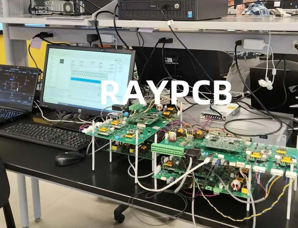
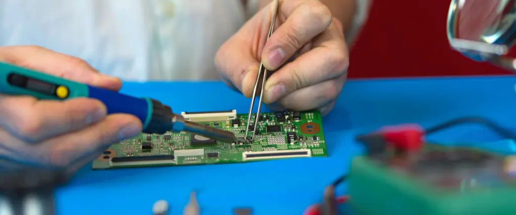
Printed Circuit Board (PCB) manufacturing is a critical component of the electronics industry. As technology advances and demand for electronic devices continues to grow, manufacturers and designers are constantly seeking ways to optimize production processes and reduce costs. One such method that has gained popularity in recent years is PCB order pooling. This article will explore the concept of PCB order pooling, its benefits, drawbacks, and its impact on the PCB manufacturing industry.

What is PCB Order Pooling?

Definition

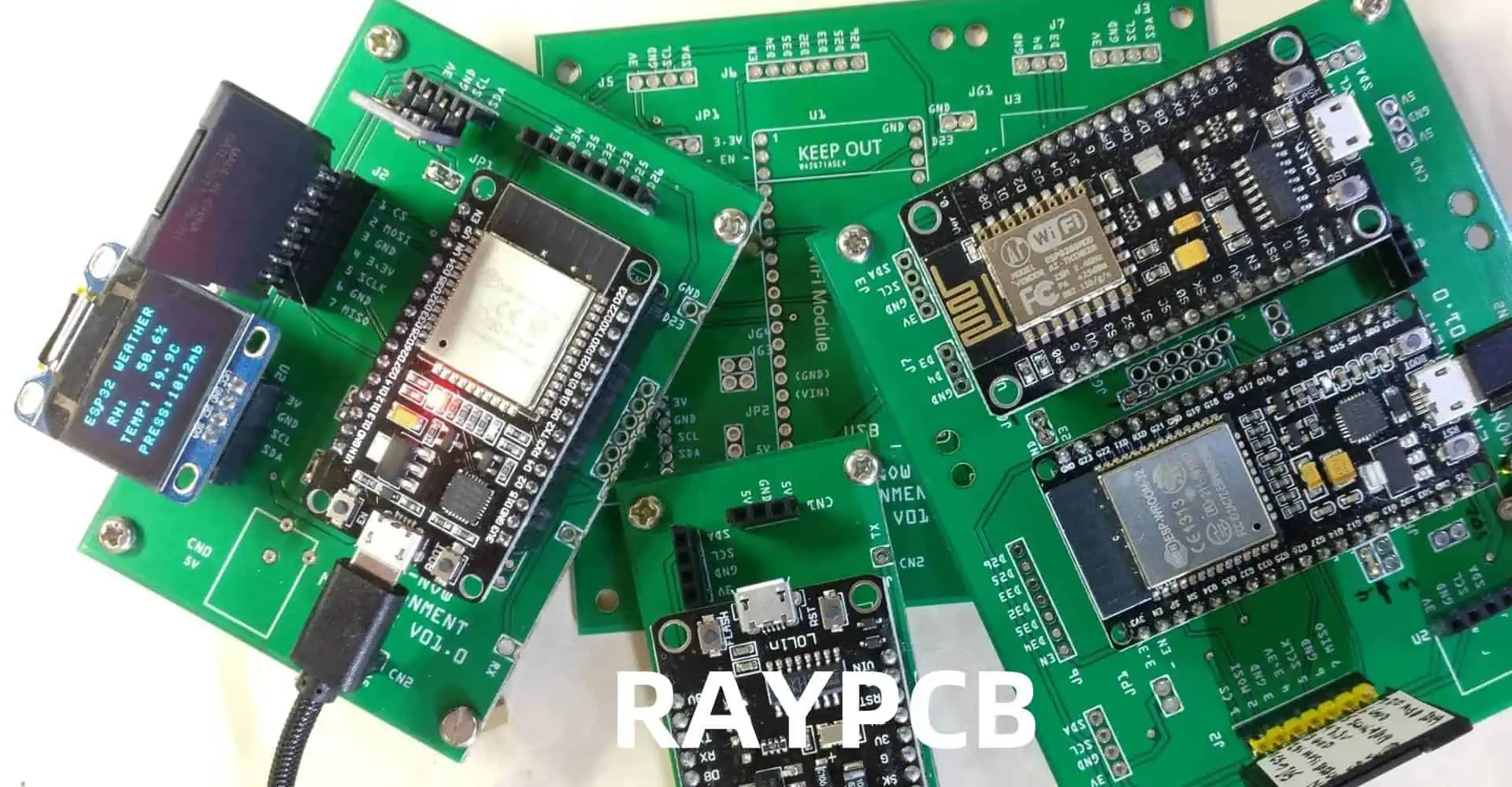
PCB order pooling, also known as PCB panel sharing or PCB aggregation, is a manufacturing strategy where multiple small PCB orders from different customers are combined into a single larger production run. This approach allows manufacturers to optimize their production processes and reduce costs by leveraging economies of scale.

How PCB Order Pooling Works

The process of PCB order pooling typically involves the following steps:

  1. Order collection: The manufacturer collects multiple small orders from various customers.
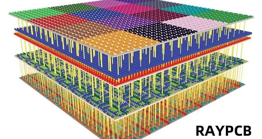
  2. Design aggregation: The individual PCB designs are arranged onto a larger panel.
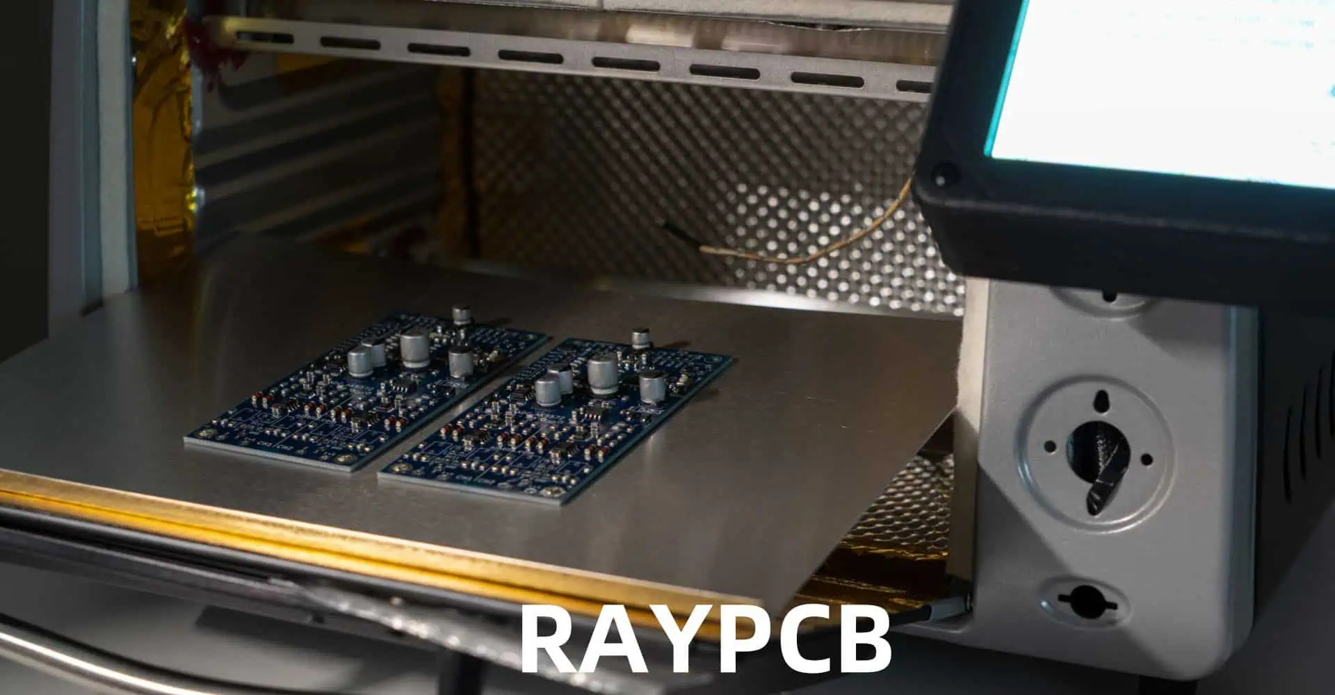
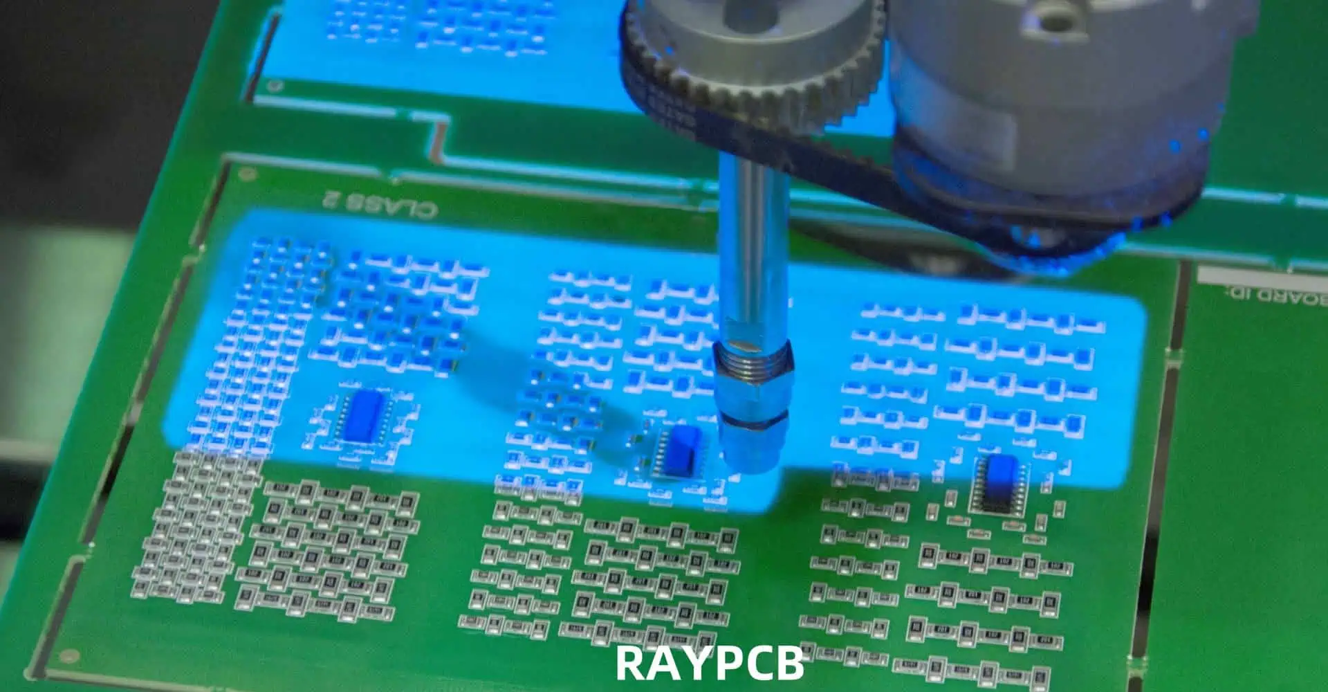
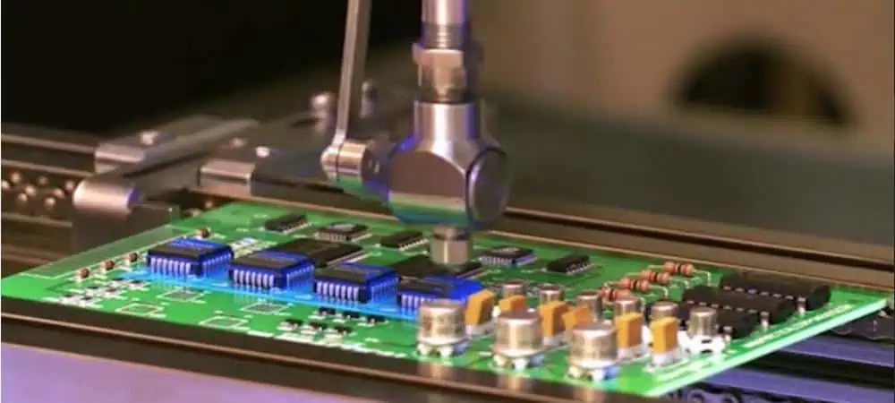
  3. Production: The combined panel is manufactured as a single unit.
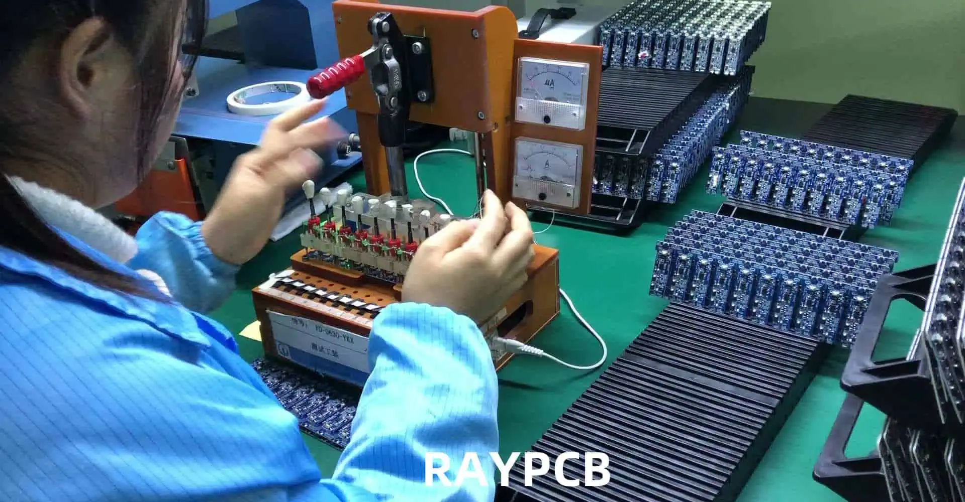
  4. Separation and quality control: The panel is separated into individual PCBs, which are then inspected and prepared for shipping.
  5. Distribution: Each customer receives their specific PCB order.

Advantages of PCB Order Pooling

Cost Reduction

One of the primary benefits of PCB order pooling is the significant cost reduction it offers, especially for small-volume orders. By combining multiple orders, manufacturers can:

  1. Reduce material waste
  2. Optimize machine setup time
  3. Lower overall production costs

Faster Turnaround Times

PCB order pooling can lead to quicker turnaround times for small orders. Since the pooled orders are processed together, customers can benefit from:

  1. Reduced wait times for production slots
  2. Faster overall manufacturing process
  3. Quicker delivery of finished PCBs

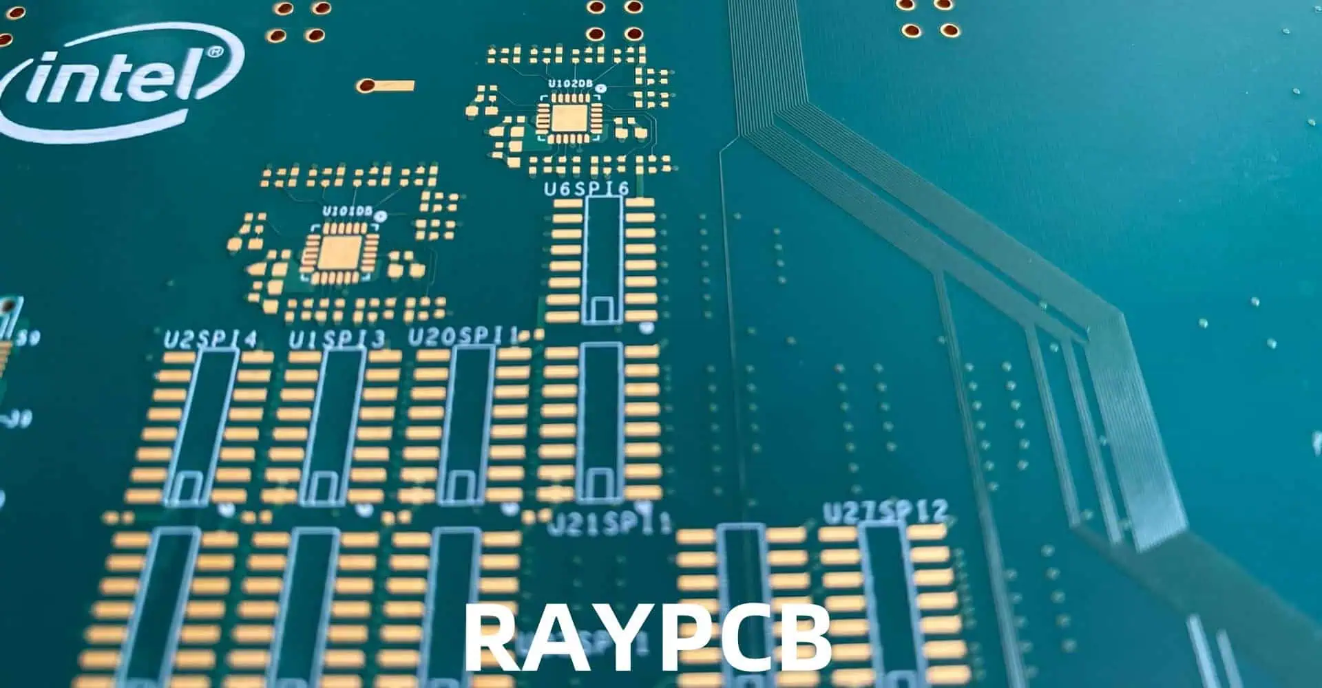
Access to Advanced Technologies

Small-volume orders often face limitations in terms of the manufacturing technologies available to them due to cost constraints. PCB order pooling allows smaller orders to benefit from:

  1. Advanced manufacturing processes
  2. Higher-quality materials
  3. Sophisticated quality control measures

Environmental Benefits

By optimizing material usage and reducing waste, PCB order pooling contributes to environmental sustainability in the following ways:

  1. Lower energy consumption per PCB produced
  2. Reduced material waste
  3. Decreased chemical usage in the manufacturing process

Disadvantages of PCB Order Pooling

Limited Customization Options

One of the main drawbacks of PCB order pooling is the potential limitation on customization options. Customers may face restrictions in terms of:

  1. Board thickness
  2. Material selection
  3. Surface finishes
  4. Special manufacturing requirements

Potential for Delays

While PCB order pooling can lead to faster turnaround times in many cases, there is also the potential for delays:

  1. Waiting for the panel to fill up with orders
  2. Addressing quality issues that affect the entire panel
  3. Coordinating multiple customer requirements

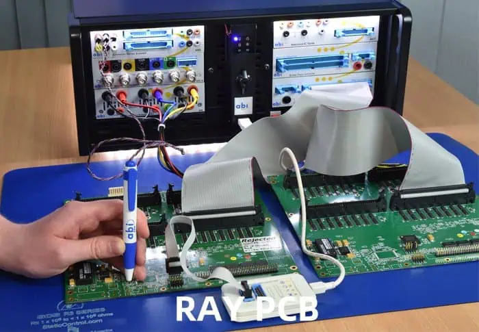
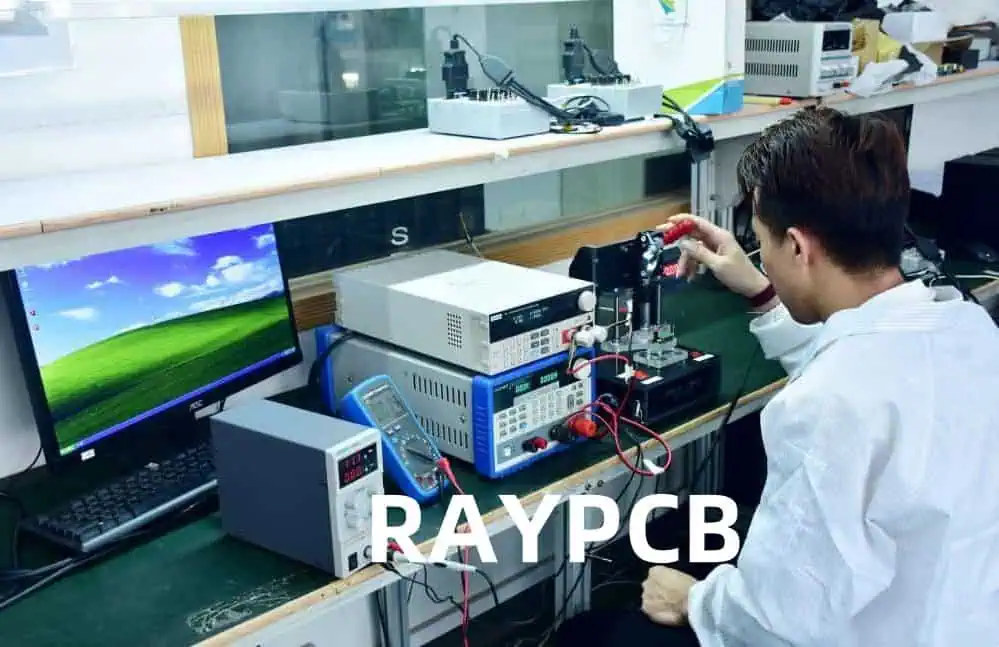
Quality Control Challenges

Combining multiple designs on a single panel can introduce quality control challenges:

  1. Increased complexity in inspection processes
  2. Potential for cross-contamination between designs
  3. Difficulty in tracing issues back to specific orders

Intellectual Property Concerns

Some customers may have concerns about the security of their intellectual property when their designs are manufactured alongside those of other companies:

  1. Risk of design exposure to competitors
  2. Potential for inadvertent mixing of orders
  3. Concerns about confidentiality in the manufacturing process

Comparing Traditional PCB Manufacturing vs. Order Pooling

To better understand the differences between traditional PCB manufacturing and order pooling, let’s compare them across several key factors:

Factor Traditional Manufacturing Order Pooling
Cost for small volumes Higher Lower
Turnaround time Variable Generally faster for small orders
Customization options Extensive Limited
Minimum order quantity Often higher Can be very low (e.g., 1-5 pieces)
Quality control Focused on single design More complex due to multiple designs
Intellectual property protection Higher Potential concerns
Environmental impact Higher for small orders Lower due to optimized production
Access to advanced technologies Limited for small orders More accessible

Best Practices for PCB Order Pooling

To maximize the benefits and minimize the drawbacks of PCB order pooling, consider the following best practices:

For Manufacturers

  1. Implement robust quality control processes
  2. Offer clear guidelines on design requirements
  3. Provide transparent pricing and lead time information
  4. Invest in advanced panel optimization software
  5. Maintain strict confidentiality protocols

For Customers

  1. Understand the limitations of order pooling
  2. Provide clean, manufacturable designs
  3. Consider standardizing certain aspects of PCB designs
  4. Communicate clearly about any special requirements
  5. Plan ahead to accommodate potential delays

Impact on the PCB Manufacturing Industry

PCB order pooling has had a significant impact on the PCB manufacturing industry:

Market Democratization

Order pooling has made high-quality PCB manufacturing accessible to a wider range of customers, including:

  1. Small startups
  2. Individual hobbyists
  3. Academic institutions

Shift in Business Models

Many PCB manufacturers have adapted their business models to accommodate order pooling:

  1. Development of online ordering platforms
  2. Investment in automated design rule checking
  3. Creation of standardized manufacturing options

Increased Competition

The popularity of order pooling has led to increased competition among PCB manufacturers:

  1. Price pressure on small-volume orders
  2. Focus on improving turnaround times
  3. Emphasis on value-added services

Technological Advancements

To support efficient order pooling, the industry has seen advancements in:

  1. Panel optimization algorithms
  2. Automated quality control systems
  3. Integration of design and manufacturing software

Future Trends in PCB Order Pooling

As the PCB manufacturing industry continues to evolve, several trends are likely to shape the future of order pooling:

Artificial Intelligence and Machine Learning

AI and ML technologies are expected to play a significant role in optimizing PCB order pooling:

  1. Improved panel optimization algorithms
  2. Predictive quality control measures
  3. Smart scheduling and production planning

Increased Automation

Automation will continue to streamline the order pooling process:

  1. Automated design rule checking and optimization
  2. Robotic handling and inspection systems
  3. Seamless integration of ordering and production systems

Expansion of Materials and Technologies

Order pooling is likely to expand to include a wider range of materials and manufacturing technologies:

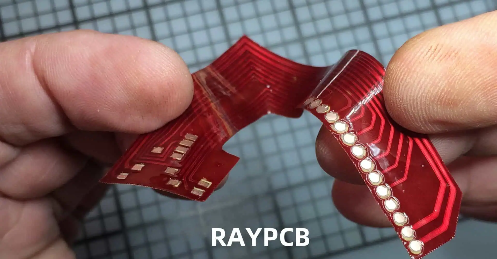
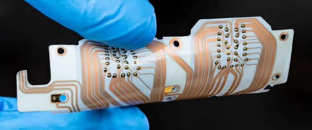
  1. Flexible and rigid-flex PCBs
  2. Advanced substrate materials
  3. Additive manufacturing techniques

Enhanced Security Measures

To address intellectual property concerns, we can expect to see:

  1. Blockchain-based traceability systems
  2. Advanced encryption for design files
  3. Improved separation and handling protocols

Conclusion

PCB order pooling has revolutionized the PCB manufacturing industry, making high-quality PCBs more accessible and affordable for small-volume orders. While it offers significant advantages in terms of cost reduction, faster turnaround times, and access to advanced technologies, it also comes with challenges related to customization, quality control, and intellectual property protection.

As the industry continues to evolve, we can expect to see further innovations in order pooling processes, driven by advancements in technology and changing customer demands. For both manufacturers and customers, understanding the pros and cons of PCB order pooling is crucial for making informed decisions and maximizing the benefits of this manufacturing approach.

By following best practices and staying informed about industry trends, businesses can leverage PCB order pooling to their advantage, whether they are producing prototypes pcba, small production runs, or specialized electronic devices.

FAQ

  1. Q: Is PCB order pooling suitable for all types of PCB designs? A: While PCB order pooling is beneficial for many designs, it may not be ideal for all types. It’s most suitable for standard designs with common specifications. Highly complex or specialized PCBs with unique requirements may be better suited for traditional manufacturing methods.
  2. Q: How does PCB order pooling affect the confidentiality of my design? A: Reputable manufacturers implement strict confidentiality protocols to protect customer designs. However, there is a slightly increased risk of design exposure compared to dedicated manufacturing runs. If you have highly sensitive designs, discuss your concerns with the manufacturer or consider alternative production methods.
  3. Q: Can I still get my PCBs quickly if I use order pooling? A: In many cases, order pooling can result in faster turnaround times, especially for small volumes. However, the exact timeline can depend on factors such as current demand and panel fill rates. Some manufacturers offer expedited services for an additional fee if you need your PCBs urgently.
  4. Q: Are there any limitations on board size or layer count when using PCB order pooling? A: Most PCB order pooling services have some limitations on board size and layer count to maintain efficiency. Typically, they accommodate boards up to a certain size (e.g., 100 x 100 mm) and layer counts up to 4 or 6 layers. For larger or more complex boards, you may need to use traditional manufacturing methods.
  5. Q: How does the quality of PCBs produced through order pooling compare to traditionally manufactured PCBs? A: When done correctly, the quality of PCBs produced through order pooling can be comparable to traditionally manufactured PCBs. Reputable manufacturers use the same high-quality materials and processes for pooled orders. However, due to the nature of combining multiple designs, there may be slightly less flexibility in terms of specific quality control measures for individual boards.

How to Bake PCBs and Components – 2024 Comprehensive Guide

In the ever-evolving world of electronics manufacturing and repair, baking printed circuit boards (PCBs) and components has become an essential process. This comprehensive guide for 2024 will explore the reasons for baking, the various methods employed, and the best practices to ensure optimal results. Whether you’re a hobbyist working on a DIY project or a professional in the electronics industry, understanding the intricacies of PCB and component baking can significantly improve the quality and reliability of your electronic assemblies.

Understanding the Need for Baking

Moisture Sensitivity

One of the primary reasons for baking PCBs and components is to remove moisture. Electronic components, especially those with plastic packaging, can absorb moisture from the environment. This absorbed moisture can lead to various issues during the soldering process.

Common Issues Caused by Moisture

  1. Popcorning: Internal steam pressure causes package cracking
  2. Delamination: Separation of internal layers
  3. Interfacial separation: Weakening of connections between different materials
  4. Oxidation: Accelerated degradation of metallic parts

Types of Components Requiring Baking

Component TypeSensitivity LevelTypical Baking Requirements
BGAsHigh125ยฐC for 24 hours
QFPsMedium to High125ยฐC for 16-24 hours
SOICsMedium125ยฐC for 12-16 hours
Passive componentsLow to Medium80-100ยฐC for 1-4 hours
PCBsVaries80-125ยฐC for 4-8 hours

Baking Equipment

pcb baking
pcb baking

Ovens for PCB and Component Baking

Conventional Ovens

  • Pros: Widely available, cost-effective
  • Cons: Less precise temperature control, potential for hot spots

Dedicated Baking Ovens

  • Pros: Precise temperature control, uniform heating
  • Cons: Higher cost, may require specialized training

Vacuum Ovens

  • Pros: Efficient moisture removal, reduced oxidation risk
  • Cons: Expensive, limited capacity

Essential Features of Baking Equipment

  1. Accurate temperature control (ยฑ1ยฐC)
  2. Good temperature uniformity across the baking chamber
  3. Proper ventilation to remove moisture
  4. Timer function for precise baking duration
  5. ESD-safe design for sensitive components

Preparing for the Baking Process

Assessing Moisture Sensitivity Levels (MSL)

MSLFloor LifeConditions
1Unlimitedโ‰ค30ยฐC / 85% RH
21 yearโ‰ค30ยฐC / 60% RH
2a4 weeksโ‰ค30ยฐC / 60% RH
3168 hoursโ‰ค30ยฐC / 60% RH
472 hoursโ‰ค30ยฐC / 60% RH
548 hoursโ‰ค30ยฐC / 60% RH
5a24 hoursโ‰ค30ยฐC / 60% RH
6TOLโ‰ค30ยฐC / 60% RH

Organizing Components and PCBs

  1. Sort components by MSL
  2. Use appropriate ESD-safe containers or trays
  3. Ensure proper spacing for uniform heat distribution
  4. Label containers with baking parameters and start time

Preheating the Oven

  1. Set the oven to the required temperature
  2. Allow sufficient time for the oven to reach and stabilize at the set temperature
  3. Use a calibrated thermometer to verify oven temperature accuracy

Baking Process for PCBs

Standard Baking Procedure

  1. Preheat oven to 125ยฐC (257ยฐF)
  2. Place PCBs in ESD-safe containers or on clean, non-conductive surfaces
  3. Ensure proper spacing between boards for uniform heating
  4. Bake for 4-8 hours, depending on board thickness and complexity
  5. Allow boards to cool naturally to room temperature before handling

Special Considerations for Different PCB Types

Rigid PCBs

  • Standard baking procedure usually sufficient
  • Longer baking times may be needed for thicker boards

Flexible PCBs

  • Use lower temperatures (80-100ยฐC) to prevent warping
  • Extend baking time to compensate for lower temperature

Rigid-Flex PCBs

  • Bake at intermediate temperatures (100-115ยฐC)
  • Monitor closely for any signs of delamination or warping

Post-Baking Handling

  1. Allow PCBs to cool to room temperature (15-30 minutes)
  2. Handle with ESD-safe gloves
  3. Store in a dry environment (preferably with desiccant)
  4. Process boards within MSL floor life or rebake if necessary

Baking Process for Components

PCB Legend solder mask oven
PCB Legend & solder mask oven

General Guidelines

  1. Refer to manufacturer’s recommendations for baking parameters
  2. Sort components by MSL and required baking conditions
  3. Use appropriate ESD-safe trays or containers
  4. Ensure proper spacing for uniform heat distribution

Baking Parameters for Common Component Types

Component TypeTemperatureDurationSpecial Notes
BGAs125ยฐC24 hoursCritical to follow exact specifications
QFPs125ยฐC16-24 hoursMonitor for lead oxidation
SOICs125ยฐC12-16 hoursEnsure proper cooling before handling
Passive components80-100ยฐC1-4 hoursGroup by size for uniform heating

Rebaking Considerations

  • Components can typically be rebaked 3-5 times before potential degradation
  • Keep track of baking cycles for each batch of components
  • Extend baking time by 25% for each rebake cycle

Advanced Baking Techniques

Vacuum Baking

  1. Place components or PCBs in a vacuum oven
  2. Set temperature and vacuum level according to manufacturer’s specifications
  3. Bake for the recommended duration (usually shorter than conventional baking)
  4. Allow gradual cooling and pressure equalization before removing items

Nitrogen Environment Baking

  1. Use a nitrogen-purged oven to create an inert atmosphere
  2. Set temperature according to standard baking requirements
  3. Maintain a slight positive pressure of nitrogen during the baking process
  4. Cool components or PCBs in the nitrogen atmosphere before removal

Step-Down Temperature Baking

  1. Start with a higher temperature (e.g., 125ยฐC) for a shorter duration
  2. Gradually reduce temperature in steps (e.g., 100ยฐC, 80ยฐC)
  3. Extend baking time at lower temperatures
  4. Helps prevent thermal shock while ensuring thorough moisture removal

Quality Control and Verification

Visual Inspection

  1. Check for any signs of physical damage or discoloration
  2. Inspect solder joints for proper wetting and appearance
  3. Look for any warping or delamination in PCBs

Weighing Method

  1. Weigh components or PCBs before and after baking
  2. Calculate moisture loss percentage
  3. Verify against expected moisture loss for the material

Electrical Testing

  1. Perform basic continuity and resistance tests
  2. Conduct functional tests where applicable
  3. Compare results with pre-baking benchmarks

X-ray Inspection

  1. Use X-ray imaging to detect internal defects
  2. Particularly useful for BGAs and other complex packages
  3. Compare pre- and post-baking images for any changes

Best Practices and Tips

  1. Always refer to manufacturer’s guidelines for specific components
  2. Maintain a clean, dry environment for post-baking storage
  3. Use moisture-sensitive indicators and desiccants in storage containers
  4. Regularly calibrate baking ovens and measurement equipment
  5. Keep detailed records of baking parameters and results
  6. Train personnel on proper baking procedures and handling techniques

Environmental and Safety Considerations

Energy Efficiency

  1. Batch components with similar baking requirements
  2. Use energy-efficient ovens with good insulation
  3. Consider solar or other renewable energy sources for baking operations

Workplace Safety

  1. Ensure proper ventilation in baking areas
  2. Use appropriate personal protective equipment (PPE) when handling hot items
  3. Implement safety protocols for oven operation and maintenance

Waste Reduction

  1. Optimize baking schedules to minimize energy waste
  2. Properly dispose of any damaged components or PCBs
  3. Recycle packaging materials where possible

Future Trends in PCB and Component Baking

PCB baking oven
PCB baking oven

AI-Driven Baking Processes

  1. Machine learning algorithms to optimize baking parameters
  2. Predictive maintenance for baking equipment
  3. Automated quality control systems

Advanced Materials

  1. Development of moisture-resistant component packaging
  2. New PCB materials with improved moisture handling characteristics
  3. Smart materials that indicate moisture levels without baking

Integration with Industry 4.0

  1. IoT-enabled baking ovens for remote monitoring and control
  2. Blockchain-based tracking of component baking history
  3. Virtual reality training for baking procedures

Conclusion

Baking PCBs and components remains a critical process in electronics manufacturing and repair as we move through 2024. By understanding the principles behind baking, employing the right techniques, and staying abreast of technological advancements, electronics professionals can ensure the reliability and longevity of their products. As the industry continues to evolve, so too will the methods and technologies used in PCB and component baking, making it an exciting field to watch in the coming years.

Frequently Asked Questions

Q1: How can I determine if my components or PCBs need baking?

A1: Several factors indicate the need for baking:

  1. Check the Moisture Sensitivity Level (MSL) of the components. If they’ve exceeded their floor life, baking is necessary.
  2. If components or PCBs have been exposed to high humidity environments.
  3. When you observe issues like popcorning or delamination during soldering.
  4. If you’re unsure about the storage history of the components.
  5. As a precautionary measure before critical or high-reliability assemblies.

Always refer to the manufacturer’s guidelines, as some components may be damaged by unnecessary baking.

Q2: What are the risks of over-baking PCBs or components?

A2: Over-baking can lead to several issues:

  1. Oxidation of component leads or PCB copper traces.
  2. Degradation of plastic packages, potentially affecting their structural integrity.
  3. Warping or delamination of PCBs, especially multi-layer boards.
  4. Changes in the electrical characteristics of some components.
  5. Reduced solderability due to excessive oxidation.

To avoid these risks, always follow the recommended baking times and temperatures, and avoid repeated baking cycles when possible.

Q3: Can I use a regular kitchen oven for baking PCBs and components?

A3: While it’s possible to use a kitchen oven, it’s not recommended for several reasons:

  1. Kitchen ovens often have poor temperature control and uniformity.
  2. They may introduce contaminants from food residues.
  3. There’s a risk of cross-contamination with food items.
  4. Kitchen ovens typically lack ESD protection.
  5. They may not reach or maintain the precise temperatures required for component baking.

For hobbyists, a dedicated toaster oven for electronics use can be a more suitable alternative. For professional use, always opt for specialized baking equipment designed for electronics.

Q4: How do I handle components or PCBs immediately after baking?

A4: Proper post-baking handling is crucial:

  1. Allow items to cool naturally to room temperature (typically 15-30 minutes).
  2. Use ESD-safe gloves and tools for handling.
  3. Transfer components or PCBs directly to a dry environment, preferably with desiccant.
  4. Process the items within their MSL floor life or store them in a moisture-barrier bag with desiccant.
  5. Avoid exposure to humid environments during transfer and processing.

Remember, the effectiveness of baking can be quickly negated by improper handling or exposure to moisture.

Q5: Are there any alternatives to thermal baking for moisture removal?

A5: Yes, there are alternative methods, although thermal baking remains the most common:

  1. Vacuum drying: Uses a combination of vacuum and mild heat for efficient moisture removal.
  2. Desiccant drying: Slow but gentle method using moisture-absorbing materials.
  3. Dry nitrogen storage: Preventative method that keeps components in a moisture-free environment.
  4. Chemical drying: Uses moisture-reactive chemicals, but risks contamination.
  5. Microwave drying: Fast but risky due to potential component damage.

Each method has its pros and cons, and the choice depends on the specific components, time constraints, and available equipment. For most applications, conventional thermal baking remains the safest and most reliable option.

Curtain Coating – High-Speed with Low Material Loss LPI Applying Method

In the world of printed circuit board (PCB) manufacturing, efficiency and precision are paramount. One of the most critical steps in PCB production is the application of liquid photoimageable (LPI) solder mask. Among the various methods available, curtain coating has emerged as a superior technique, offering high-speed application with minimal material loss. This comprehensive guide will explore the intricacies of curtain coating, its benefits, challenges, and its role in advancing PCB manufacturing technology.

Understanding Curtain Coating

What is Curtain Coating?

Curtain coating is an advanced method of applying liquid materials, such as LPI solder mask, onto substrates. In this process, a thin, continuous “curtain” of liquid is created and allowed to fall onto the substrate as it passes underneath. This method ensures uniform coverage and thickness across the entire surface.

Historical Context

Curtain coating technology was initially developed for the photographic film industry in the mid-20th century. Its adoption in PCB manufacturing began in the late 1990s and has since revolutionized the application of solder mask and other materials in the electronics industry.

The Science Behind Curtain Coating

Fluid Dynamics

Curtain coating relies on precise control of fluid dynamics. Key factors include:

  1. Viscosity of the coating material
  2. Flow rate
  3. Curtain height
  4. Substrate speed

Key Components of a Curtain Coater

ComponentFunction
Coating headCreates and shapes the liquid curtain
Pump systemControls flow rate and pressure
ConveyorMoves PCBs beneath the curtain
Edge guidesMaintains curtain stability
Recirculation systemCollects and reuses excess material

Types of Curtain Coaters

Single-Layer Curtain Coaters

  • Used for applying a single type of coating
  • Simpler design and operation
  • Ideal for standard LPI solder mask application

Multi-Layer Curtain Coaters

  • Can apply multiple layers simultaneously
  • Used for complex coating requirements
  • Enables unique material combinations

Advantages of Curtain Coating in LPI Application

High-Speed Operation

  1. Faster than traditional methods like screen printing
  2. Can coat up to 60 meters per minute or more
  3. Increases overall production throughput

Low Material Loss

  1. Precision application reduces overspray
  2. Recirculation system captures excess material
  3. Typical material savings of 20-30% compared to other methods

Uniform Coating Thickness

  1. Consistent curtain flow ensures even coverage
  2. Reduced risk of thin spots or excessive buildup
  3. Improves overall PCB quality and reliability

Reduced Defect Rates

  1. Minimal air entrapment compared to other methods
  2. Lower incidence of pinholes and bubbles
  3. Decreases rework and scrap rates

Versatility

  1. Can handle various substrate sizes and shapes
  2. Adaptable to different coating materials
  3. Suitable for rigid and flexible PCBs

Implementing Curtain Coating in PCB Manufacturing

Equipment Setup

  1. Installation of curtain coating machine
  2. Integration with existing production line
  3. Calibration and testing

Material Preparation

  1. Selection of appropriate LPI solder mask
  2. Adjustment of viscosity for optimal flow
  3. Filtration to remove particulates

Process Parameters

ParameterTypical RangeImpact
Curtain height10-50 mmAffects coating uniformity
Flow rate0.5-5 L/minDetermines coating thickness
Conveyor speed30-60 m/minInfluences production rate
Viscosity200-2000 cPAffects curtain stability

Quality Control Measures

  1. Real-time monitoring of curtain stability
  2. Thickness measurement systems
  3. Visual inspection for defects
  4. Regular maintenance and cleaning

Challenges and Solutions in Curtain Coating

Curtain Stability

Challenge: Maintaining a stable curtain, especially at high speeds. Solution:

  • Use of edge guides
  • Precise viscosity control
  • Vibration isolation systems

Substrate Wetting

Challenge: Ensuring complete wetting of the PCB surface. Solution:

  • Pre-treatment of PCB surface
  • Optimization of coating material properties
  • Adjustment of curtain impact angle

Coating Thickness Control

Challenge: Achieving consistent thickness across varying PCB topographies. Solution:

  • Dynamic flow rate adjustment
  • Multi-pass coating for complex boards
  • Advanced feedback control systems

Environmental Factors

Challenge: Sensitivity to temperature and humidity variations. Solution:

  • Climate-controlled coating environment
  • Real-time adjustment of process parameters
  • Use of temperature-stable coating materials

Optimizing Curtain Coating Performance

Material Selection

  1. Choose LPI solder masks designed for curtain coating
  2. Consider viscosity stability over time
  3. Evaluate curing characteristics

Equipment Maintenance

  1. Regular cleaning of coating heads
  2. Inspection and replacement of wear parts
  3. Calibration of flow control systems

Operator Training

  1. Understanding of fluid dynamics principles
  2. Troubleshooting skills
  3. Interpretation of quality control data

Process Monitoring and Control

  1. Implementation of vision systems for curtain inspection
  2. Use of advanced process control algorithms
  3. Data logging and analysis for continuous improvement

Environmental and Economic Considerations

Reduced Material Waste

  1. Lower overspray compared to spray coating
  2. Efficient material recirculation
  3. Decreased disposal costs

Energy Efficiency

  1. Lower curing energy requirements due to uniform coating
  2. Reduced need for rework and reprocessing
  3. Optimized production flow

VOC Emissions

  1. Potential for using low-VOC or VOC-free materials
  2. Enclosed coating environment for emission control
  3. Compliance with environmental regulations

Future Trends in Curtain Coating Technology

Advanced Materials

  1. Development of new LPI formulations optimized for curtain coating
  2. Integration of functional additives (e.g., flame retardants, thermal management)
  3. Exploration of bio-based and sustainable coating materials

Automation and Industry 4.0

  1. Integration with smart factory systems
  2. Real-time process optimization using AI and machine learning
  3. Predictive maintenance capabilities

Miniaturization Support

  1. Adaptation for coating ultra-fine pitch PCBs
  2. Development of thin, uniform coatings for flexible electronics
  3. Integration with advanced PCB manufacturing techniques

Case Studies

Large-Scale PCB Manufacturer

A major PCB manufacturer implemented curtain coating, resulting in:

  • 40% increase in production speed
  • 25% reduction in material consumption
  • 50% decrease in defect rates

Flexible PCB Specialist

A flexible PCB producer adopted curtain coating, achieving:

  • Improved coating uniformity on flexible substrates
  • 30% reduction in production costs
  • Expansion into new market segments

Conclusion

Curtain coating represents a significant advancement in LPI solder mask application for PCB manufacturing. Its ability to combine high-speed operation with low material loss makes it an attractive option for manufacturers seeking to improve efficiency and quality. While challenges exist, ongoing technological developments continue to enhance the capabilities of curtain coating systems.

As the electronics industry evolves, with trends towards miniaturization, flexibility, and sustainability, curtain coating is well-positioned to meet these demands. By offering precise, uniform, and efficient coating application, this technology will play a crucial role in shaping the future of PCB manufacturing.

Frequently Asked Questions

Q1: How does curtain coating compare to traditional screen printing for LPI solder mask application?

A1: Curtain coating offers several advantages over traditional screen printing:

  1. Higher speed: Curtain coating can operate at speeds up to 60 meters per minute or more, significantly faster than screen printing.
  2. Better uniformity: It provides a more consistent coating thickness across the entire PCB surface.
  3. Lower material waste: With its recirculation system, curtain coating typically uses 20-30% less material than screen printing.
  4. Reduced defects: There’s less risk of air entrapment, resulting in fewer pinholes and bubbles.
  5. Versatility: Curtain coating can handle a wider range of substrate sizes and shapes more easily.

However, screen printing may still be preferred for very small production runs or highly specialized applications where the setup time for curtain coating might not be justified.

Q2: What are the main factors affecting coating thickness in curtain coating?

A2: The main factors influencing coating thickness in curtain coating are:

  1. Flow rate: The volume of coating material dispensed per unit time.
  2. Conveyor speed: The speed at which the PCB moves under the curtain.
  3. Curtain height: The distance between the coating head and the PCB surface.
  4. Viscosity: The thickness or flow resistance of the coating material.
  5. Surface tension: Affects how the coating material spreads on the PCB surface.

These factors are interrelated, and adjusting one often requires fine-tuning of the others to maintain optimal coating quality.

Q3: Can curtain coating be used for other PCB manufacturing processes besides LPI solder mask application?

A3: Yes, curtain coating technology can be adapted for various PCB manufacturing processes, including:

  1. Application of etch resists
  2. Conformal coatings
  3. Applying legend inks
  4. Depositing conductive inks in printed electronics
  5. Applying adhesives for flexible PCB lamination

The versatility of curtain coating makes it a valuable tool for many liquid application processes in electronics manufacturing.

Q4: How does curtain coating address the challenge of coating PCBs with varying topographies?

A4: Curtain coating addresses varying PCB topographies through several mechanisms:

  1. Fluid dynamics: The curtain’s momentum helps it conform to surface variations.
  2. Optimized viscosity: Proper viscosity allows the coating to flow into recesses and over raised areas.
  3. Multiple passes: Complex boards may receive multiple coating layers.
  4. Dynamic flow control: Advanced systems can adjust flow rates in real-time based on board topography.
  5. Pre-coating surface treatment: Enhances wetting and coverage of challenging areas.

While curtain coating is generally very effective, extremely complex topographies may still require supplementary techniques or specialized coating materials.

Q5: What are the key maintenance requirements for a curtain coating system?

A5: Proper maintenance is crucial for optimal curtain coating performance. Key maintenance requirements include:

  1. Regular cleaning of the coating head to prevent nozzle clogs and ensure consistent flow.
  2. Inspection and replacement of wear parts such as pumps, seals, and filters.
  3. Calibration of flow control systems and sensors to maintain accuracy.
  4. Cleaning and maintenance of the recirculation system to prevent contamination.
  5. Regular checks of the conveyor system for alignment and wear.
  6. Monitoring and maintaining the environmental control systems (temperature, humidity).
  7. Periodic full system checks and preventative maintenance schedules.

Adhering to these maintenance practices helps ensure consistent coating quality, minimize downtime, and extend the life of the equipment.

How to Remove Soldermask from Printed Circuit Boards?

Soldermask is a thin layer of polymer applied to printed circuit boards (PCBs) to protect the copper traces from oxidation and prevent solder bridges between closely spaced solder pads. While soldermask is crucial for most PCB applications, there are instances where its removal becomes necessary. This comprehensive guide will explore various methods, tools, and precautions for removing soldermask from PCBs effectively and safely.

Understanding Soldermask

What is Soldermask?

Soldermask, also known as solder resist, is a thin layer of polymer applied to the copper traces of a PCB. Its primary functions include:

  1. Protecting copper traces from oxidation
  2. Preventing solder bridges between adjacent pads
  3. Improving the board’s appearance
  4. Providing electrical insulation

Types of Soldermask

TypeCharacteristicsCommon Applications
Liquid Photoimageable (LPI)UV-curable, high resolutionMost commercial PCBs
Dry FilmPre-formed film, uniform thicknessHigh-end PCBs, flexible circuits
Epoxy-basedHeat-curable, durableIndustrial and military applications
Acrylic-basedFast curing, flexibleConsumer electronics

Reasons for Removing Soldermask

Common Scenarios

  1. Repair and rework of PCBs
  2. Modification of existing circuits
  3. Improving electrical connections
  4. Exposing copper for grounding purposes
  5. Reverse engineering

Considerations Before Removal

  • Necessity of removal
  • Extent of removal (partial or complete)
  • PCB material and soldermask type
  • Available tools and equipment
  • Safety precautions

Methods for Removing Soldermask

Mechanical Removal

Scraping

  1. Use a sharp craft knife or scalpel
  2. Gently scrape the soldermask layer
  3. Be careful not to damage underlying copper

Pros:

  • Simple and inexpensive
  • Precise control over removal area

Cons:

  • Time-consuming for large areas
  • Risk of damaging copper traces

Sanding

  1. Use fine-grit sandpaper (400-600 grit)
  2. Gently sand the soldermask in circular motions
  3. Clean debris with compressed air or brush

Pros:

  • Effective for larger areas
  • Relatively quick

Cons:

  • Less precise than scraping
  • May thin copper layer if not careful

Chemical Removal

Soldermask Remover Solutions

  1. Apply commercial soldermask remover
  2. Allow to sit for recommended time
  3. Scrub gently with a soft brush
  4. Rinse thoroughly with water
  5. Neutralize if required

Pros:

  • Effective for large areas
  • Less risk of mechanical damage

Cons:

  • Chemical exposure risks
  • May affect other components

Acetone or Paint Stripper

  1. Apply acetone or paint stripper to a cloth
  2. Rub gently on soldermask area
  3. Repeat until soldermask is removed
  4. Clean thoroughly with isopropyl alcohol

Pros:

  • Readily available materials
  • Effective on some soldermask types

Cons:

  • May not work on all soldermask types
  • Can potentially damage certain PCB materials

Thermal Removal

Heat Gun Method

  1. Set heat gun to appropriate temperature (300-400ยฐC)
  2. Apply heat evenly to soldermask area
  3. Scrape softened soldermask with a plastic tool
  4. Clean residue with isopropyl alcohol

Pros:

  • Effective for stubborn soldermask
  • Can cover larger areas quickly

Cons:

  • Risk of overheating and damaging board
  • Requires careful temperature control

Soldering Iron Method

Plugged Via with Solder Mask
  1. Set soldering iron to medium-high temperature
  2. Gently rub the iron tip over soldermask
  3. Scrape away softened soldermask
  4. Clean area with isopropyl alcohol

Pros:

  • Precise control for small areas
  • Common tool in most electronics workshops

Cons:

  • Time-consuming for large areas
  • Risk of overheating nearby components

Laser Removal

  1. Use a laser engraving machine with appropriate settings
  2. Program the area for soldermask removal
  3. Run the laser removal process
  4. Clean the area with compressed air and alcohol

Pros:

  • Highly precise and controllable
  • Minimal risk of mechanical damage

Cons:

  • Expensive equipment required
  • Learning curve for proper settings

Tools and Materials

ToolPurpose
Craft knife or scalpelScraping and precision removal
Fine-grit sandpaperLarger area removal
Heat gunThermal removal method
Soldering ironPrecision thermal removal
Plastic scraperRemoving softened soldermask
Soft-bristled brushCleaning and scrubbing

Essential Tools

Materials

  • Isopropyl alcohol
  • Acetone (for some methods)
  • Commercial soldermask remover
  • Safety equipment (gloves, goggles, mask)
  • Lint-free cloths
  • Compressed air canister

Step-by-Step Guide to Soldermask Removal

Preparation

  1. Identify the area for soldermask removal
  2. Choose the appropriate method based on area size and PCB characteristics
  3. Gather necessary tools and materials
  4. Set up a well-ventilated workspace
  5. Put on safety equipment

Removal Process

For Mechanical Removal:

  1. Start with the gentlest method (scraping)
  2. Gradually increase pressure or move to sanding if necessary
  3. Frequently clean the area to monitor progress
  4. Be extra cautious around delicate traces and components

For Chemical Removal:

  1. Apply chemical remover according to manufacturer’s instructions
  2. Allow proper dwell time
  3. Gently scrub with a soft brush
  4. Rinse thoroughly and neutralize if required
  5. Repeat if necessary

For Thermal Removal:

  1. Set equipment to appropriate temperature
  2. Apply heat evenly to the target area
  3. Use plastic scraper to remove softened soldermask
  4. Clean area thoroughly after removal

Post-Removal Cleanup

  1. Inspect the area for complete soldermask removal
  2. Clean thoroughly with isopropyl alcohol
  3. Use compressed air to remove any debris
  4. Inspect copper traces for any damage
  5. Apply conformal coating if leaving copper exposed

Safety Precautions

General Safety

  • Work in a well-ventilated area
  • Wear appropriate personal protective equipment (PPE)
  • Keep a first aid kit nearby
  • Be aware of fire hazards when using thermal methods

Chemical Safety

  • Read and follow all material safety data sheets (MSDS)
  • Use chemical-resistant gloves
  • Avoid skin contact or inhalation of fumes
  • Have an eyewash station or sink nearby

Electrical Safety

  • Disconnect PCB from power sources before working
  • Be cautious of static electricity when handling sensitive components
  • Use ESD-safe tools and workspace when necessary

Best Practices and Tips

  1. Always start with the least aggressive method
  2. Test the chosen method on a small, non-critical area first
  3. Take frequent breaks to avoid fatigue-induced mistakes
  4. Keep tools clean and in good condition
  5. Document the process, especially for complex boards
  6. Consider professional services for critical or valuable PCBs

Environmental Considerations

Proper Disposal

  • Dispose of chemical waste according to local regulations
  • Recycle PCB scrap when possible
  • Use environmentally friendly cleaning products when available

Minimizing Waste

  • Remove only as much soldermask as necessary
  • Use precision tools to minimize overspray or excess removal
  • Reuse cleaning cloths when possible

Alternatives to Soldermask Removal

When to Consider Alternatives

  • If removal risks damaging the PCB
  • When only temporary access is needed
  • If full removal is not necessary for the task

Alternative Approaches

  1. Using conductive paint for small connections
  2. Careful drilling for via access
  3. Adding new traces or jumper wires
  4. Using press-fit hardware for grounding points

Reapplying Soldermask

When to Reapply

  • After completing necessary modifications
  • To protect exposed copper from oxidation
  • When restoring board to original specifications

Reapplication Methods

  1. UV-curable liquid soldermask
  2. Epoxy-based soldermask pens
  3. Aerosol soldermask sprays

Troubleshooting Common Issues

IssuePossible CauseSolution
Incomplete removalInsufficient time or pressureRepeat process or try a more aggressive method
Damage to copper tracesExcessive force or heatUse gentler techniques, consider professional repair
Chemical residueInadequate cleaningThorough cleaning with appropriate solvents
Uneven removalInconsistent techniquePractice on scrap boards, use guides for evenness
Soldermask not softeningWrong removal method for typeResearch soldermask type and choose appropri

Conclusion

Removing soldermask from PCBs is a delicate process that requires careful consideration of the board’s characteristics, the reason for removal, and the available tools and methods. By following the techniques outlined in this guide and adhering to safety precautions, you can successfully remove soldermask when necessary. Remember to always start with the least aggressive method and prioritize the integrity of the PCB and its components throughout the process.

Frequently Asked Questions

Q1: Can I remove soldermask from a populated PCB?

A1: While it’s possible, it’s generally not recommended to remove soldermask from a populated PCB due to the risk of damaging components. If necessary, use extreme caution, opt for precise methods like careful scraping or chemical removal, and protect surrounding components with masking tape or conformal coating. Consider desoldering sensitive components before soldermask removal if possible.

Q2: How do I identify the type of soldermask on my PCB?

A2: Identifying the exact type can be challenging without specialized equipment, but you can make educated guesses based on appearance and board origin. Green LPI soldermask is most common in commercial PCBs. Glossy finishes often indicate epoxy-based masks, while matte finishes might be acrylic. For precise identification, consult the PCB manufacturer or consider sending a sample for analysis if critical.

Q3: Is it safe to use a laser engraver for soldermask removal?

A3: Laser engraving can be an effective and precise method for soldermask removal, but it requires proper equipment and expertise. Use a laser engraver designed for PCB work, ensure proper ventilation due to fumes, and carefully calibrate power and speed settings to avoid damaging the underlying copper or FR-4 substrate. Always start with conservative settings and test on a non-critical area first.

Q4: How do I remove soldermask from flexible PCBs?

A4: Flexible PCBs require extra care due to their delicate nature. Chemical methods are often preferred, using solvents specifically designed for flexible PCB soldermask. Mechanical methods risk damaging the flexible substrate. If using thermal methods, use very low temperatures and be extremely cautious. Always support the flexible PCB on a flat surface during the removal process to prevent bending or stress.

Q5: Can soldermask removal affect the PCB’s electrical characteristics?

A5: Yes, removing soldermask can potentially affect a PCB’s electrical characteristics, especially in high-frequency applications. Soldermask acts as a dielectric layer and its removal can change impedance characteristics, increase susceptibility to noise, and potentially lead to short circuits if conductive debris bridges traces. After removal, consider applying a conformal coating to protect exposed copper and maintain some of the electrical isolation properties.

How to Make RoHS Certified Electronic Products

In today’s environmentally conscious world, producing electronic products that meet international standards for hazardous substance restriction is not just a regulatory requirement but also a moral imperative. The Restriction of Hazardous Substances (RoHS) directive, initially implemented by the European Union, has become a global benchmark for manufacturing safer and more environmentally friendly electronic products. This article will guide you through the process of creating RoHS certified electronic products, from understanding the directive to implementing changes in your manufacturing process.

Understanding RoHS

What is RoHS?

RoHS, which stands for Restriction of Hazardous Substances, is a directive that restricts the use of specific hazardous materials found in electrical and electronic products. Originally adopted by the EU in 2003, it has since been adopted and adapted by various countries worldwide.

RoHS Restricted Substances

The RoHS directive restricts the use of ten hazardous substances:

SubstanceMaximum Permitted Concentration
Lead (Pb)0.10%
Mercury (Hg)0.10%
Cadmium (Cd)0.01%
Hexavalent Chromium (Cr6+)0.10%
Polybrominated Biphenyls (PBB)0.10%
Polybrominated Diphenyl Ethers (PBDE)0.10%
Bis(2-Ethylhexyl) phthalate (DEHP)0.10%
Butyl benzyl phthalate (BBP)0.10%
Dibutyl phthalate (DBP)0.10%
Diisobutyl phthalate (DIBP)0.10%

Scope of RoHS

RoHS applies to a wide range of electrical and electronic equipment, including:

  1. Large household appliances
  2. Small household appliances
  3. IT and telecommunications equipment
  4. Consumer equipment
  5. Lighting equipment
  6. Electrical and electronic tools
  7. Toys, leisure, and sports equipment
  8. Medical devices (with some exceptions)
  9. Monitoring and control instruments
  10. Automatic dispensers

Steps to Achieve RoHS Compliance

REACH vs RoHS
REACH vs RoHS

1. Assess Your Current Products

Conduct a Product Inventory

Create a comprehensive list of all your products and their components.

Identify Non-Compliant Materials

Review each component and material used in your products to identify any that contain restricted substances above the permitted levels.

2. Supplier Engagement

Communicate with Suppliers

Inform your suppliers about your RoHS compliance goals and request information on the materials they provide.

Obtain Declarations of Conformity

Request RoHS compliance certificates or declarations from your suppliers for all components and materials.

3. Material Substitution

Identify Alternatives

Research and identify RoHS-compliant alternatives for any non-compliant materials or components.

Test New Materials

Thoroughly test new materials to ensure they meet both RoHS requirements and your product performance standards.

4. Update Manufacturing Processes

Review Production Techniques

Examine your manufacturing processes to identify any steps that might introduce restricted substances.

Implement New Procedures

Develop and implement new procedures to ensure RoHS compliance throughout the manufacturing process.

5. Employee Training

Educate Your Team

Provide comprehensive training to all relevant employees on RoHS requirements and new procedures.

Designate RoHS Compliance Officers

Assign responsibility for ongoing RoHS compliance to specific team members.

6. Documentation and Record Keeping

Create a Compliance File

Maintain a detailed record of all steps taken to achieve RoHS compliance, including supplier declarations, test results, and process changes.

Implement a Document Control System

Establish a system to manage and update RoHS-related documentation regularly.

7. Testing and Verification

Conduct Regular Testing

Implement a schedule for regular testing of your products to ensure ongoing compliance.

Use Accredited Laboratories

Utilize accredited testing facilities to perform RoHS compliance tests.

8. Certification and Labeling

Obtain RoHS Certification

Once compliance is achieved and verified, obtain official RoHS certification for your products.

Apply RoHS Compliance Marks

Label your products with the appropriate RoHS compliance marks.

Challenges in Achieving RoHS Compliance

rohs tester

Technical Challenges

Performance Issues

Some RoHS-compliant alternatives may not perform as well as their restricted counterparts, necessitating design changes.

Reliability Concerns

Certain RoHS-compliant materials, such as lead-free solders, may have different reliability characteristics, requiring additional testing and validation.

Supply Chain Challenges

Supplier Compliance

Ensuring all suppliers in your supply chain are RoHS compliant can be a complex and time-consuming process.

Global Sourcing Issues

Different regions may have varying interpretations or implementations of RoHS, complicating global sourcing efforts.

Cost Implications

Cost FactorPotential Impact
Material SubstitutionHigher costs for RoHS-compliant alternatives
Process ChangesInvestment in new equipment or procedures
Testing and CertificationOngoing expenses for compliance verification
TrainingCosts associated with employee education

Regulatory Complexity

Keeping Up with Changes

RoHS regulations are subject to periodic reviews and updates, requiring ongoing vigilance and adaptation.

Regional Variations

Different countries or regions may have their own versions of RoHS with slight variations in requirements.

Benefits of RoHS Compliance

Environmental Impact

RoHS compliance significantly reduces the amount of hazardous substances entering the environment through electronic waste.

Market Access

RoHS compliance allows access to markets that require adherence to these standards, particularly the European Union.

Brand Reputation

Demonstrating commitment to environmental responsibility can enhance brand image and customer loyalty.

Legal Compliance

Adhering to RoHS standards helps avoid potential legal issues and penalties in regulated markets.

Future Trends in RoHS and Electronic Product Compliance

Expansion of Restricted Substances

The list of restricted substances under RoHS is likely to grow as new environmental and health concerns emerge.

Global Harmonization

Efforts are underway to harmonize RoHS-like regulations globally, potentially simplifying compliance for manufacturers.

Integration with Other Environmental Regulations

RoHS compliance is increasingly being integrated with other environmental and sustainability initiatives, such as energy efficiency standards and circular economy principles.

Advanced Testing Methods

New technologies for rapid and non-destructive testing of RoHS compliance are being developed, which could streamline the verification process.

Conclusion

Achieving RoHS certification for electronic products is a complex but necessary process in today’s global market. It requires a comprehensive approach involving every aspect of product design, sourcing, and manufacturing. While the journey to RoHS compliance can be challenging, the benefits โ€“ including environmental protection, market access, and enhanced brand reputation โ€“ make it a worthwhile endeavor.

By following the steps outlined in this guide and staying informed about regulatory changes, manufacturers can successfully navigate the path to RoHS compliance. As environmental concerns continue to shape consumer preferences and regulatory landscapes, RoHS compliance will remain a crucial aspect of electronic product manufacturing for the foreseeable future.

Ultimately, the pursuit of RoHS compliance not only ensures legal and market compliance but also contributes to the broader goal of creating a more sustainable and responsible electronics industry. As technology continues to advance, the principles behind RoHS will likely play an increasingly important role in shaping the future of electronic product design and manufacturing.

Frequently Asked Questions (FAQ)

1. How long does it typically take to achieve RoHS compliance for a product?

The time required to achieve RoHS compliance can vary significantly depending on the complexity of the product and the current state of your manufacturing processes. For a relatively simple product with a straightforward supply chain, it might take 3-6 months. For more complex products or those requiring significant redesign, the process could take up to a year or more. Key factors affecting the timeline include:

  • The number of components and materials in your product
  • The complexity of your supply chain
  • The extent of changes required in your manufacturing processes
  • The availability of RoHS-compliant alternatives for your materials

It’s important to note that achieving compliance is an ongoing process, not a one-time event, as you’ll need to maintain compliance through regular audits and updates.

2. Can a product be partially RoHS compliant?

No, a product cannot be partially RoHS compliant. RoHS compliance is an all-or-nothing proposition โ€“ every component and material in the product must meet the RoHS requirements for the entire product to be considered compliant. However, it’s worth noting that some components may be exempt from RoHS requirements if they fall under specific exemptions listed in the RoHS directive. These exemptions are typically for applications where no viable alternative exists or where the reliability of alternatives is not yet proven.

3. How do I verify if a supplier’s components are truly RoHS compliant?

Verifying supplier compliance involves several steps:

  1. Request formal documentation: Ask for RoHS compliance certificates or declarations of conformity.
  2. Review test reports: Request and review any available test reports from accredited laboratories.
  3. Conduct audits: Consider conducting supplier audits, especially for critical components.
  4. Perform random testing: Implement a program of random testing on received components.
  5. Use XRF analyzers: For quick, non-destructive testing, X-ray fluorescence (XRF) analyzers can be useful tools.

Remember, while these steps can provide a high level of assurance, absolute certainty can only come from comprehensive testing of the final product.

4. What are the penalties for non-compliance with RoHS?

Penalties for non-compliance with RoHS can be severe, although they vary by jurisdiction. In the European Union, for example, penalties can include:

  • Fines: These can range from thousands to millions of euros, depending on the severity and scale of the non-compliance.
  • Market withdrawal: Non-compliant products may be required to be withdrawn from the market.
  • Import bans: Repeated non-compliance can result in bans on importing products into the EU.
  • Criminal charges: In some cases, willful non-compliance can result in criminal charges against company officials.

Beyond these direct penalties, non-compliance can also lead to significant damage to brand reputation and loss of market share.

5. Does RoHS compliance automatically ensure compliance with similar regulations in other countries?

While RoHS compliance is a good starting point, it doesn’t automatically ensure compliance with similar regulations in all countries. Many countries have adopted RoHS-like regulations, but there can be important differences in the details. For example:

  • China RoHS has some different labeling requirements.
  • California’s Electronic Waste Recycling Act has some additional substances restricted.
  • Some countries may have different exemptions or implementation timelines.

Therefore, while RoHS compliance puts you in a good position, it’s important to verify the specific requirements for each market you plan to enter. Always check the most current regulations for your target markets, as these can change over time.

Functional Testing of PCB Assembly and PCBA FCT Costs

In the world of electronics manufacturing, ensuring the quality and reliability of printed circuit board assemblies (PCBAs) is paramount. Functional testing plays a crucial role in this process, verifying that each PCBA operates as intended before it reaches the end-user. This article delves into the intricacies of functional testing for PCB assemblies, exploring various testing methods, their importance, and the associated costs. We’ll also examine how these costs can impact overall production and ways to optimize the testing process for efficiency and cost-effectiveness.

Understanding Functional Testing in PCBA

What is Functional Testing?

Functional testing, also known as Functional Circuit Testing (FCT), is a critical step in the PCBA manufacturing process. It involves powering up the assembled PCB and testing its functionality to ensure it performs according to design specifications.

Importance of Functional Testing

Quality Assurance

Functional testing serves as the final quality check before a PCBA is shipped or integrated into a larger system.

Defect Detection

It helps identify issues that may not be apparent through visual inspection or other testing methods.

Performance Verification

FCT confirms that the PCBA meets the required performance standards and specifications.

Types of Functional Tests

Test TypeDescriptionTypical Applications
Power-On TestVerifies basic power supply functionalityAll PCBAs
Signal Integrity TestChecks signal quality and timingHigh-speed digital circuits
Communication Interface TestValidates various communication protocolsPCBAs with network capabilities
Sensor and Actuator TestVerifies functionality of input/output devicesIoT devices, automotive electronics
Environmental Stress TestChecks performance under various environmental conditionsMilitary, aerospace a

Functional Testing Process

Pre-Test Preparation

  1. Developing test plans and procedures
  2. Creating test fixtures and programming test equipment
  3. Calibrating test instruments

Test Execution

Manual Testing

Involves human operators performing tests using various instruments and following predefined procedures.

Automated Testing

Utilizes computerized test equipment and software to perform a series of predefined tests automatically.

Post-Test Analysis

  1. Data collection and analysis
  2. Defect categorization
  3. Reporting and documentation

Factors Affecting PCBA FCT Costs

Test Equipment Costs

Automated Test Equipment (ATE)

High-end ATE systems can cost hundreds of thousands of dollars but offer faster and more consistent testing.

Specialized Instruments

Oscilloscopes, multimeters, and other specialized testing instruments contribute to overall equipment costs.

Test Fixture Costs

Custom fixtures designed for specific PCBAs can be a significant expense, especially for complex or unique designs.

Labor Costs

Testing ApproachLabor IntensitySkill Level Required
Manual TestingHighMedium to High
Semi-Automated TestingMediumMedium
Fully Automated TestingLowHigh (for setup and maintenance)

Test Development Costs

  1. Test plan creation
  2. Test software development
  3. Fixture design and fabrication

Production Volume Impact

Production VolumeCost per UnitInitial Setup Cost
Low VolumeHigherLower
High VolumeLowerHigher

Complexity of PCBA

More complex PCBAs with numerous components and functions typically require more extensive and costly testing procedures.

Strategies for Optimizing FCT Costs

Design for Testability (DFT)

Implementing DFT principles during the PCB design phase can significantly reduce testing complexity and costs.

Key DFT Practices

  1. Including test points and access pads
  2. Designing modular circuits
  3. Implementing self-test features

Test Coverage Optimization

Balancing test coverage with testing time and costs to achieve optimal quality assurance.

Automation Implementation

While initially costly, automating the testing process can lead to long-term cost savings, especially for high-volume production.

In-Circuit Test (ICT) vs. Functional Test Trade-offs

Test TypeAdvantagesDisadvantages
In-Circuit TestFaster, better fault isolationHigher fixture costs, limited functional testing
Functional TestComprehensive performance verificationLonger test times, more complex setup

Combining ICT and FCT can often provide a cost-effective solution with comprehensive test coverage.

Standardization and Reusability

Developing standardized test procedures and reusable test fixtures can reduce costs across multiple projects.

Emerging Trends in PCBA Functional Testing

Industry 4.0 and Smart Manufacturing

Integration of FCT data with manufacturing execution systems (MES) for real-time quality control and process optimization.

Artificial Intelligence and Machine Learning

Using AI/ML algorithms to:

  1. Predict potential defects
  2. Optimize test sequences
  3. Analyze test data for continuous improvement

Virtual and Augmented Reality in Testing

VR/AR technologies can assist in:

  1. Test operator training
  2. Guided testing procedures
  3. Remote troubleshooting

Cost-Benefit Analysis of Functional Testing

Short-Term vs. Long-Term Costs

AspectShort-Term ImpactLong-Term Impact
Equipment InvestmentHigh initial costReduced per-unit testing cost
Quality ImprovementImmediate defect reductionEnhanced brand reputation, fewer returns
Process OptimizationInitial disruptionIncreased efficiency and throughput

ROI Calculation

Factors to consider in Return on Investment (ROI) calculation:

  1. Reduction in field failures and warranty claims
  2. Increased production yield
  3. Reduced rework and scrap costs
  4. Improved customer satisfaction and retention

Case Studies: FCT Implementation and Cost Analysis

Case Study 1: High-Volume Consumer Electronics

A smartphone manufacturer implemented automated FCT, resulting in:

  • 30% reduction in overall testing time
  • 50% decrease in field failure rates
  • 20% increase in production yield

Initial investment was recouped within 18 months.

Case Study 2: Low-Volume, High-Complexity Aerospace PCBAs

An aerospace company optimized its FCT process for low-volume, high-complexity PCBAs:

  • Developed modular test fixtures
  • Implemented AI-assisted test sequence optimization
  • Achieved 40% reduction in test development time
  • Improved fault detection rate by 25%

Future of PCBA Functional Testing

5G and High-Speed Circuit Testing

As 5G technology becomes more prevalent, new testing methodologies for high-speed circuits will be required.

IoT and Edge Computing Challenges

The proliferation of IoT devices will necessitate more sophisticated and efficient testing procedures to handle diverse functionality and connectivity options.

Sustainability in Testing

Growing emphasis on sustainable manufacturing practices will drive the development of more energy-efficient testing methods and equipment.

Conclusion

Functional testing of PCB assemblies is a critical process that ensures the quality and reliability of electronic products. While it represents a significant cost in the manufacturing process, the benefits of comprehensive FCT far outweigh the expenses when considering long-term product reliability and customer satisfaction.

As technology continues to evolve, so too will the methods and tools used in PCBA functional testing. Manufacturers who invest in optimizing their testing processes and embrace new technologies stand to gain a competitive edge in terms of both product quality and production efficiency.

The key to successful and cost-effective functional testing lies in finding the right balance between test coverage, automation, and adaptability to changing technological landscapes. By carefully considering the factors affecting FCT costs and implementing strategies to optimize the testing process, manufacturers can ensure high-quality PCBAs while managing production costs effectively.

Frequently Asked Questions (FAQ)

1. How long does functional testing typically take for a PCBA?

The duration of functional testing can vary significantly depending on the complexity of the PCBA and the extent of testing required. For simple PCBAs, functional testing might take only a few minutes per board. However, for complex PCBAs or those requiring extensive environmental testing, the process could take hours or even days. On average, functional testing for a moderately complex PCBA might take anywhere from 5 to 30 minutes per board.

2. Can functional testing detect all possible defects in a PCBA?

While functional testing is comprehensive, it cannot guarantee the detection of all possible defects. It is excellent at identifying operational issues and verifying that the PCBA functions as intended under normal conditions. However, some latent defects or issues that only manifest under specific circumstances might not be detected. This is why functional testing is often used in conjunction with other testing methods like in-circuit testing, visual inspection, and environmental stress testing for more complete coverage.

3. How does the cost of functional testing compare to other testing methods?

The cost of functional testing generally falls between in-circuit testing (ICT) and visual inspection in terms of per-unit cost. Here’s a rough comparison:

Testing MethodRelative CostTest Coverage
Visual InspectionLowLimited
In-Circuit TestingMedium-HighGood for component-level defects
Functional TestingMediumExcellent for operational verification
Burn-in TestingHighBest for reliability issues

The actual costs can vary significantly based on production volume, PCBA complexity, and specific testing requirements.

4. Is it possible to reduce functional testing costs without compromising quality?

Yes, there are several strategies to reduce functional testing costs while maintaining quality:

  1. Implement Design for Testability (DFT) principles
  2. Optimize test coverage to focus on critical functions
  3. Automate testing processes where possible
  4. Develop reusable test fixtures and procedures
  5. Combine functional testing with other testing methods strategically
  6. Continuously analyze and improve the testing process

The key is to focus on efficiency and effectiveness rather than simply cutting corners.

5. How often should functional test equipment and procedures be updated?

Functional test equipment and procedures should be reviewed and potentially updated:

  1. When new product designs are introduced
  2. If there are significant changes in manufacturing processes
  3. When new technologies or testing methodologies become available
  4. If there’s an increase in field failures or quality issues
  5. At regular intervals (e.g., annually) as part of continuous improvement efforts

Regular updates ensure that the testing process remains effective, efficient, and aligned with current technological standards and product requirements.

PCB Manual Soldering Guide You Need to Know

Manual soldering is a fundamental skill in electronics manufacturing and repair. Whether you’re a hobbyist working on a DIY project or a professional in the field, understanding the intricacies of PCB (Printed Circuit Board) soldering is crucial. This comprehensive guide will walk you through the essential techniques, tools, and best practices for manual PCB soldering, ensuring you can create reliable and high-quality connections.

Understanding PCB Soldering

What is PCB Soldering?

PCB soldering is the process of joining electronic components to a printed circuit board using molten solder. This creates both mechanical and electrical connections, allowing the circuit to function as designed. Manual soldering, as opposed to automated methods, involves a hands-on approach using a soldering iron and other tools.

The Importance of Proper Soldering

Proper soldering is critical for several reasons:

  1. Electrical conductivity
  2. Mechanical strength
  3. Reliability and longevity of the circuit
  4. Prevention of short circuits and other faults

Poor soldering can lead to intermittent connections, component failure, and overall circuit malfunction.

Essential Tools for PCB Soldering

Soldering Iron

The soldering iron is your primary tool. Here are key factors to consider:

Temperature Control

  • Low-end irons: Fixed temperature
  • Mid-range irons: Adjustable temperature
  • High-end stations: Precise digital control

Wattage

  • 15-30W: Suitable for small components and delicate work
  • 30-60W: Ideal for general-purpose PCB soldering
  • 60W+: Necessary for large components or ground planes

Tip Types

Tip Shape Best Use Case
Conical Precision work, small components
Chisel General-purpose soldering
Bevel Drag soldering, large pads
Hoof Desoldering, removing solder

Solder

Choosing the right solder is crucial for successful PCB soldering.

Composition

  • Lead-based: Easier to work with, but environmental concerns
  • Lead-free: Environmentally friendly, higher melting point

Diameter

  • 0.5mm – 0.8mm: Fine pitch components
  • 0.8mm – 1.2mm: General-purpose soldering
  • 1.2mm+: Large components, heavy-duty work

Flux Core

Flux helps clean the surfaces and promote better solder flow. Most electronic solder comes with a flux core.

Other Essential Tools

  • Desoldering pump or wick
  • Flux pen or liquid flux
  • Wire cutters and pliers
  • Tweezers
  • Magnifying glass or loupe
  • Multimeter
  • Fume extractor

Preparing for Soldering

Workspace Setup

  1. Choose a well-ventilated area
  2. Use a non-conductive, heat-resistant work surface
  3. Ensure good lighting
  4. Keep your work area clean and organized

Safety Precautions

  • Wear safety glasses
  • Use a fume extractor or work in a well-ventilated area
  • Never touch the hot end of the soldering iron
  • Wash hands after soldering to remove flux residue

PCB and Component Preparation

  1. Clean the PCB with isopropyl alcohol
  2. Inspect components for damage
  3. Pre-tin component leads if necessary
  4. Secure the PCB in a helping hand or PCB holder

Basic Soldering Techniques

Through-Hole Soldering

  1. Insert the component into the PCB
  2. Bend leads slightly to hold it in place
  3. Heat the pad and lead simultaneously
  4. Apply solder to the junction, not the iron tip
  5. Remove heat and allow the joint to cool
  6. Trim excess lead length

Surface Mount Soldering

Drag Soldering

  1. Apply flux to the pads
  2. Align the component
  3. Tack one corner pin
  4. Verify alignment and adjust if needed
  5. Apply solder to the iron tip
  6. Drag the iron across the pins
  7. Use solder wick to remove bridges

Individual Pin Soldering

  1. Apply flux to the pads
  2. Place the component
  3. Solder one corner pin
  4. Verify alignment
  5. Solder remaining pins individually
  6. Clean excess flux

Advanced Soldering Techniques

PTH Soldering
PTH Soldering

Fine-Pitch Components

  1. Use a fine-tip soldering iron
  2. Apply liquid flux
  3. Use minimal solder
  4. Consider using a hot air rework station for very fine pitch

BGA (Ball Grid Array) Rework

BGA soldering typically requires specialized equipment, but for repair:

  1. Apply flux to the BGA pads
  2. Align the BGA carefully
  3. Use a hot air rework station to reflow solder
  4. Allow to cool slowly
  5. Inspect with X-ray if possible

Desoldering Techniques

Using a Solder Sucker

  1. Heat the solder joint
  2. Place the solder sucker over the melted solder
  3. Quickly press the button to suck up the solder
  4. Repeat if necessary

Using Desoldering Wick

  1. Place the wick on the solder joint
  2. Heat the wick with the iron
  3. As the solder melts, it will be drawn into the wick
  4. Move to a clean section of wick and repeat if needed

Soldering Best Practices

Temperature Control

Component Type Recommended Temperature Range
Small components 315ยฐC – 340ยฐC (600ยฐF – 650ยฐF)
General-purpose 340ยฐC – 370ยฐC (650ยฐF – 700ยฐF)
Large components 370ยฐC – 400ยฐC (700ยฐF – 750ยฐF)

Tip Care and Maintenance

  1. Keep the tip tinned when not in use
  2. Clean the tip frequently using a damp sponge or brass wool
  3. Replace tips when they become pitted or deformed

Avoiding Common Mistakes

  • Cold joints: Ensure proper heating of both the pad and component
  • Overheating: Work quickly and efficiently
  • Bridging: Use appropriate amount of solder and clean excess
  • Disturbed joints: Allow joints to cool completely before moving

Inspection and Quality Control

Visual Inspection

Look for:

  • Smooth, shiny solder joints
  • Proper wetting and fillet formation
  • No solder bridges or excess solder
  • No visible damage to components or PCB

Electrical Testing

  1. Continuity testing
  2. Voltage and current measurements
  3. Functional testing of the circuit

Rework and Repair

If issues are found:

  1. Identify the problem
  2. Choose appropriate rework technique
  3. Re-solder or replace components as needed
  4. Re-inspect and test

Environmental Considerations

Lead-Free Soldering

  • Higher melting point (requires higher temperatures)
  • May require different flux formulations
  • Can result in duller-looking joints (still functional)

Proper Disposal

  • Recycle scrap PCBs and components
  • Dispose of lead-containing solder as hazardous waste
  • Follow local regulations for electronic waste disposal

Troubleshooting Common Soldering Issues

Issue Possible Causes Solutions
Cold joint Insufficient heat, movement during cooling Reheat and add small amount of solder
Solder bridges Excess solder, poor technique Use solder wick to remove excess
Lifted pads Overheating, mechanical stress Secure pad, use jumper wire if necessary
Burned components Excessive heat, poor heat sinking Replace component, use heat sink clips
Dry joint Contamination, insufficient flux Clean thoroughly, add flux, resolder

Continuing Education and Skill Development

PCB soldering problems
  • Practice regularly with various component types
  • Stay updated on new soldering technologies and techniques
  • Consider certification programs (e.g., IPC-A-610)
  • Join electronics communities and forums for knowledge sharing

Conclusion

Manual PCB soldering is both an art and a science. With the right tools, techniques, and practice, you can achieve professional-quality results. Remember to prioritize safety, maintain your equipment, and continually refine your skills. Whether you’re working on prototypes assembly board, repairs, or small-scale production, mastering manual soldering will prove invaluable in your electronics journey.

Frequently Asked Questions

Q1: How do I choose the right soldering iron for PCB work?

A1: Consider factors such as adjustable temperature control, appropriate wattage (30-60W for most PCB work), and interchangeable tips. Look for models with good thermal recovery and a comfortable grip. For beginners, a mid-range soldering station with digital temperature control is often a good starting point.

Q2: What’s the difference between lead and lead-free solder for PCB work?

A2: Lead solder (typically 60/40 or 63/37 tin-lead) has a lower melting point, flows better, and is easier to work with. However, it’s being phased out due to environmental concerns. Lead-free solder (often SAC305) has a higher melting point, can be more difficult to work with, and may produce duller-looking joints, but it’s more environmentally friendly and compliant with modern regulations.

Q3: How can I prevent damaging sensitive components while soldering?

A3: Use temperature-controlled soldering irons, work quickly and efficiently, use heat sinks on sensitive component leads, and avoid overheating. For very sensitive components, consider using anti-static precautions. Always double-check the component’s maximum temperature rating and adjust your soldering technique accordingly.

Q4: What’s the best way to remove solder bridges between fine-pitch components?

A4: First, apply a small amount of flux to the bridged area. Then, use fine desoldering braid (wick) to remove the excess solder. Place the wick on top of the bridge and apply heat with your soldering iron. As the solder melts, it will be drawn into the wick. Move to a clean section of wick and repeat if necessary. For very fine pitch components, you may need to use a hot air rework station or a specialized fine-tip soldering iron.

Q5: How often should I clean and tin my soldering iron tip?

A5: Clean your tip frequently during use, ideally after every few solder joints. Use a damp sponge or brass wool for cleaning. Tin the tip (apply a small amount of fresh solder) whenever you set the iron down or finish a soldering session. This prevents oxidation and extends the life of your tip. Replace tips when they become pitted, deformed, or no longer hold solder properly.

Does Your PCB Assembly Need Conformal Coating?

In the world of electronics manufacturing, printed circuit boards (PCBs) are the backbone of countless devices. As these devices become more complex and are used in increasingly diverse environments, protecting PCB assemblies from external factors becomes crucial. One of the most effective methods of protection is conformal coating. This article explores the concept of conformal coating, its benefits, applications, and helps you determine whether your PCB assembly needs this protective measure.

What is Conformal Coating?

Definition and Purpose

Conformal coating is a thin protective chemical coating applied to PCB assemblies to protect the electronic components from environmental stresses. The coating “conforms” to the contours of the PCB, providing a uniform protective layer.

YouTube video

Types of Conformal Coatings

There are several types of conformal coatings, each with its own characteristics and applications:

Coating TypeKey FeaturesBest For
Acrylic (AR)Easy to apply and remove, good moisture resistanceGeneral purpose, prototyping
Urethane (UR)Excellent chemical and abrasion resistanceHarsh chemical environments
Silicone (SR)High temperature resistance, very flexibleExtreme temperatures, high humidity
Epoxy (ER)Strong chemical and abrasion resistanceDemanding environments, long-term protection
ParyleneThin, uniform coating, excellent barrier propertiesMedical devices, aerospace applications

Application Methods

Conformal coatings can be applied using various techniques:

  1. Dipping
  2. Spraying
  3. Brushing
  4. Selective coating
  5. Vapor deposition (for Parylene)

Each method has its advantages and is chosen based on the PCB design, production volume, and required precision.

Benefits of Conformal Coating

Conformal Coating

Environmental Protection

Moisture Resistance

Conformal coatings create a barrier against moisture, preventing corrosion and electrical shorts.

Temperature Resistance

Certain coatings can protect PCBs from extreme temperatures, both hot and cold.

Chemical Protection

Coatings shield components from exposure to harmful chemicals and solvents.

Mechanical Protection

Vibration and Shock Resistance

Coatings can absorb some of the stress from vibrations and shocks, protecting delicate components.

Abrasion Protection

The coating layer guards against physical wear and tear.

Electrical Benefits

Improved Dielectric Strength

Coatings increase the insulation between components, reducing the risk of arcing and short circuits.

Prevention of Dendrite Growth

Coatings inhibit the growth of conductive dendrites that can cause short circuits over time.

Extended Lifespan

By protecting against various environmental and physical stresses, conformal coatings can significantly extend the life of PCB assemblies.

When to Consider Conformal Coating

Environmental Factors

Consider conformal coating if your PCB will be exposed to:

  1. High humidity or moisture
  2. Salt spray or corrosive atmospheres
  3. Extreme temperatures
  4. Chemicals or solvents

Application-Specific Requirements

Certain industries and applications often require conformal coating:

IndustryCommon Requirements
AutomotiveTemperature extremes, vibration, chemicals
AerospaceAltitude changes, temperature fluctuations
MarineHigh humidity, salt spray
IndustrialChemicals, dust, vibration
MedicalBiocompatibility, sterilization resistance

Regulatory Compliance

Some industries have regulations that mandate the use of conformal coatings for safety and reliability.

Factors to Consider Before Applying Conformal Coating

PCB Design Considerations

Component Selection

Some components may not be suitable for coating or may require masking.

Layout and Spacing

Adequate spacing between components is necessary for proper coating coverage.

Test Points and Connectors

Areas that require electrical contact may need to be masked before coating.

Cost Analysis

While conformal coating adds to the production cost, it should be weighed against:

  1. Potential warranty claims
  2. Product failures in the field
  3. Brand reputation damage

Production Process Impact

Implementing conformal coating may require:

  1. Additional equipment
  2. Extended production time
  3. Quality control measures

Repairability

Coated PCBs can be more challenging to repair, which should be considered for products that may require field servicing.

The Conformal Coating Process

Pre-Coating Preparation

  1. Cleaning the PCB assembly
  2. Masking areas that should not be coated
  3. Pre-heating (if required)

Coating Application

The chosen application method is used to apply the coating evenly across the PCB.

Curing

Depending on the coating type, curing may involve:

  1. Heat curing
  2. UV curing
  3. Moisture curing
  4. Room temperature curing

Quality Control

Post-coating inspection may include:

  1. Visual inspection
  2. Thickness measurement
  3. Continuity testing

Challenges and Considerations

Conformal Coating
Conformal Coating

Common Issues

IssueCauseSolution
BubblesTrapped air, improper applicationAdjust application technique, use vacuum to remove air
DelaminationPoor surface preparation, incompatible materialsImprove cleaning process, choose compatible coating
Incomplete coverageImproper application techniqueAdjust application method, multiple coats if necessary
Orange peel effectImproper spraying techniqueAdjust spray parameters, consider dif

Material Compatibility

Ensure the chosen coating is compatible with:

  1. PCB substrate material
  2. Component materials
  3. Solder mask
  4. Labels and markings

Thickness Control

Maintaining the right coating thickness is crucial for:

  1. Adequate protection
  2. Avoiding excess weight
  3. Preventing thermal insulation issues

Masking and Keep-Out Areas

Proper masking is essential for:

  1. Connectors
  2. Test points
  3. Adjustable components
  4. Heat sinks

Alternatives to Conformal Coating

Potting and Encapsulation

For extreme environments, potting the entire PCB in a protective resin may be more suitable.

Sealed Enclosures

Using hermetically sealed enclosures can provide protection without coating the PCB directly.

Ruggedized PCB Design

Designing the PCB with built-in protection features can reduce the need for additional coating.

Future Trends in Conformal Coating

Nano-Coatings

Ultra-thin nano-coatings are being developed for better protection with minimal impact on PCB properties.

Smart Coatings

Self-healing and self-diagnosing coatings are emerging technologies that could revolutionize PCB protection.

Environmentally Friendly Options

New coating formulations are focusing on reducing environmental impact and improving sustainability.

Conclusion

Conformal coating can significantly enhance the reliability and longevity of PCB assemblies, especially in challenging environments. While it adds complexity and cost to the manufacturing process, the benefits often outweigh these factors for many applications. By carefully considering the specific needs of your PCB assembly and the environment it will operate in, you can make an informed decision about whether conformal coating is necessary for your project.

As technology continues to advance, we can expect to see new coating materials and application methods that offer even better protection with fewer drawbacks. Staying informed about these developments will help ensure that your PCB assemblies remain protected and reliable in an ever-evolving technological landscape.

Frequently Asked Questions (FAQ)

Why should the PCBA brush conformal coating

1. How long does conformal coating typically last?

The lifespan of conformal coating depends on the type of coating used and the environmental conditions. Generally, a well-applied conformal coating can last anywhere from 5 to 10 years or even longer in controlled environments. However, in harsh conditions or with constant exposure to extreme temperatures or chemicals, the coating may degrade more quickly.

2. Can conformal coating be removed if repairs are needed?

Yes, conformal coating can be removed for repairs, but the process can be challenging and time-consuming. The removal method depends on the type of coating used. Some coatings can be removed with solvents, while others may require mechanical abrasion or specialized removal techniques. It’s important to note that the removal process can potentially damage components if not done carefully.

3. Are there any components that should not be coated?

Yes, certain components should not be coated or require special consideration:

  1. Connectors and sockets
  2. Switches and relays
  3. Potentiometers and trimmers
  4. Some types of sensors
  5. Components that generate significant heat

These components may need to be masked before coating or may require selective coating techniques.

4. How thick should the conformal coating be?

The ideal thickness of conformal coating typically ranges from 25 to 250 micrometers (1 to 10 mils), depending on the specific coating type and application requirements. Thinner coatings may not provide adequate protection, while excessively thick coatings can lead to issues with heat dissipation and component stress.

5. Can conformal coating affect the electrical properties of the PCB?

While conformal coating is designed to have minimal impact on electrical properties, it can affect them in some ways. The coating may slightly change the capacitance between closely spaced conductors and can impact the performance of high-frequency circuits. Additionally, some coatings may affect the dielectric constant of the PCB. These factors should be considered during the design phase, especially for sensitive or high-frequency applications.

Carbon Nanotube Material Used in PCB—New Technology

In the ever-evolving world of electronics, printed circuit boards (PCBs) play a crucial role in connecting and supporting various components. As devices become smaller, faster, and more complex, the demand for advanced PCB materials grows. One of the most promising innovations in this field is the use of carbon nanotube (CNT) materials in PCBs. This article explores the exciting new technology of carbon nanotubes in PCB manufacturing, its benefits, challenges, and potential applications.

What Are Carbon Nanotubes?

Structure and Properties

Carbon nanotubes are cylindrical molecules composed of carbon atoms arranged in a hexagonal lattice. They can be single-walled (SWCNT) or multi-walled (MWCNT), with diameters ranging from 1 to 50 nanometers and lengths up to several micrometers.

Key properties of carbon nanotubes include:

  1. Exceptional strength-to-weight ratio
  2. High thermal conductivity
  3. Excellent electrical conductivity
  4. Flexibility and durability

Types of Carbon Nanotubes

TypeStructureDiameterProperties
Single-walled (SWCNT)Single layer of carbon atoms0.4 – 2 nmHigher electrical conductivity, more flexible
Multi-walled (MWCNT)Multiple concentric layers2 – 100 nmGreater strength, thermal stability

Carbon Nanotubes in PCB Manufacturing

Integration Methods

Incorporating carbon nanotubes into PCBs can be achieved through several methods:

  1. CNT-epoxy composites
  2. CNT-metal matrix composites
  3. Direct growth of CNTs on PCB substrates
  4. CNT-based conductive inks

Each method offers unique advantages and challenges, influencing the final properties of the PCB.

Benefits of CNT-Enhanced PCBs

The integration of carbon nanotubes into PCBs brings numerous benefits:

Improved Thermal Management

Carbon nanotubes possess excellent thermal conductivity, significantly enhancing heat dissipation in PCBs. This property is crucial for high-power and high-density electronic applications.

Enhanced Electrical Performance

CNTs can improve signal integrity and reduce electromagnetic interference (EMI) due to their superior electrical properties.

Mechanical Strength and Flexibility

The incorporation of CNTs can lead to stronger, more flexible PCBs, making them suitable for wearable and flexible electronics.

Miniaturization Potential

The nanoscale dimensions of CNTs allow for the creation of smaller, more compact PCB designs.

Comparison: Traditional vs. CNT-Enhanced PCBs

PropertyTraditional PCBsCNT-Enhanced PCBs
Thermal ConductivityModerateHigh
Electrical ConductivityGoodExcellent
FlexibilityLimitedHigh
EMI ShieldingModerateImproved
WeightStandardReduced

Manufacturing Processes

CNT Production for PCB Applications

The production of high-quality carbon nanotubes for PCB applications involves several steps:

  1. Synthesis (e.g., chemical vapor deposition, arc discharge)
  2. Purification
  3. Functionalization (if required)
  4. Integration into PCB materials

PCB Fabrication with CNT Materials

Integrating CNTs into PCB manufacturing requires modifications to existing processes:

  1. Substrate preparation
  2. CNT dispersion or growth
  3. Patterning and etching
  4. Component assembly

Challenges in CNT-PCB Manufacturing

While promising, the use of CNTs in PCBs faces several challenges:

  1. Uniform dispersion of CNTs
  2. Scalability of production
  3. Cost considerations
  4. Quality control and consistency

Applications of CNT-Enhanced PCBs

High-Frequency Electronics

Carbon nanotube-enhanced PCBs are particularly suitable for high-frequency applications due to their superior signal integrity and reduced signal loss.

Aerospace and Defense

The lightweight and durable nature of CNT-PCBs makes them ideal for aerospace and defense applications, where weight reduction and reliability are critical.

Wearable Technology

The flexibility and thermal management properties of CNT-PCBs are beneficial for wearable devices, allowing for more comfortable and efficient designs.

Automotive Electronics

CNT-PCBs can withstand the harsh environments found in automotive applications while providing improved performance and reliability.

Potential Future Applications

ApplicationBenefit of CNT-PCBs
5G and 6G NetworksImproved signal integrity, reduced interference
Quantum ComputingEnhanced thermal management, reduced noise
Biomedical ImplantsFlexibility, biocompatibility, miniaturization
Space ExplorationLightweight, radiation resistance

Environmental and Safety Considerations

Ecological Impact

The use of CNTs in PCBs may have both positive and negative environmental implications:

  • Positive: Potential for longer-lasting electronics, reduced e-waste
  • Negative: Concerns about nanoparticle release during production and disposal

Safety Protocols

Handling CNTs requires specific safety measures due to their nanoscale size:

  1. Personal protective equipment (PPE)
  2. Controlled manufacturing environments
  3. Proper disposal and recycling procedures

Future Outlook and Research Directions

Ongoing Research

Current research in CNT-PCB technology focuses on:

  1. Improving CNT dispersion techniques
  2. Enhancing CNT-polymer interfaces
  3. Developing hybrid CNT-metal composites
  4. Exploring novel CNT growth methods on PCB substrates

Industry Adoption

The adoption of CNT-enhanced PCBs in the electronics industry depends on:

  1. Cost reduction in CNT production
  2. Standardization of manufacturing processes
  3. Demonstration of long-term reliability
  4. Regulatory approval and safety assurances

Potential Impact on Electronics Industry

The widespread adoption of CNT-PCBs could revolutionize the electronics industry by:

  1. Enabling more compact and powerful devices
  2. Improving energy efficiency in electronic systems
  3. Facilitating the development of flexible and wearable electronics
  4. Enhancing the performance of high-frequency and high-power applications

Conclusion

Carbon nanotube materials in PCBs represent a significant leap forward in electronic manufacturing technology. While challenges remain in terms of production scalability and cost-effectiveness, the potential benefits in terms of performance, miniaturization, and flexibility are substantial. As research progresses and manufacturing processes improve, we can expect to see an increasing adoption of CNT-enhanced PCBs across various industries, paving the way for next-generation electronic devices and systems.

Frequently Asked Questions (FAQ)

1. What are the main advantages of using carbon nanotubes in PCBs?

The main advantages include improved thermal management, enhanced electrical performance, increased mechanical strength and flexibility, and the potential for miniaturization. These properties allow for the creation of more efficient, durable, and compact electronic devices.

2. Are CNT-enhanced PCBs more expensive than traditional PCBs?

Currently, CNT-enhanced PCBs are generally more expensive due to the cost of producing high-quality carbon nanotubes and the specialized manufacturing processes required. However, as technology advances and production scales up, the cost is expected to decrease, making them more competitive with traditional PCBs.

3. How do CNT-PCBs contribute to environmental sustainability?

CNT-PCBs can contribute to environmental sustainability by potentially increasing the lifespan of electronic devices, reducing e-waste, and improving energy efficiency. However, proper disposal and recycling methods need to be developed to address concerns about nanoparticle release into the environment.

4. What industries are likely to benefit most from CNT-PCB technology?

Industries that are likely to benefit most include aerospace, defense, automotive, telecommunications, and wearable technology. These sectors can leverage the improved performance, reliability, and flexibility offered by CNT-enhanced PCBs.

5. Is it safe to use products with CNT-enhanced PCBs?

When properly manufactured and encapsulated within the PCB structure, CNT-enhanced PCBs are considered safe for consumer use. However, ongoing research is being conducted to ensure long-term safety and to develop appropriate handling and disposal protocols for manufacturers and recyclers.

DuPont Introduces Pyralux AG Flexible Circuit Materials for High-Volume Manufacturing

In a significant advancement for the electronics industry, DuPont has unveiled its latest innovation in flexible circuit materials – Pyralux AG. This cutting-edge product line is specifically designed to meet the growing demands of high-volume manufacturing in the rapidly evolving world of flexible and rigid-flex circuits. As electronic devices continue to become smaller, lighter, and more complex, the need for reliable and high-performance flexible circuit materials has never been greater. DuPont’s Pyralux AG series promises to deliver on these requirements while offering improved processability and cost-effectiveness for manufacturers.

The Evolution of Flexible Circuit Materials

Historical Context

Flexible circuits have come a long way since their inception in the early 20th century. Initially used in rudimentary applications, these versatile components have become integral to modern electronics, finding their way into everything from smartphones to medical devices and aerospace systems.

The Role of Materials Science

The development of flexible circuit materials has been closely tied to advancements in materials science. Over the years, manufacturers have sought materials that could offer:

  1. Excellent electrical properties
  2. Mechanical flexibility
  3. Thermal stability
  4. Chemical resistance
  5. Dimensional stability

DuPont, with its long history of innovation in materials science, has been at the forefront of this evolution, continuously developing new solutions to meet the changing needs of the industry.

Introducing Pyralux AG: A New Benchmark in Flexible Circuit Materials

Dupont Pyralux AP Flex PCB

Key Features of Pyralux AG

DuPont’s Pyralux AG series represents a significant leap forward in flexible circuit material technology. Some of the key features that set it apart include:

  1. Enhanced electrical performance
  2. Improved thermal reliability
  3. Superior dimensional stability
  4. Excellent chemical resistance
  5. Optimized for high-volume manufacturing processes

Material Composition

Pyralux AG is a composite material consisting of:

This carefully engineered combination results in a material that offers exceptional performance across a wide range of applications and manufacturing processes.

Advantages for High-Volume Manufacturing

Streamlined Processing

One of the primary advantages of Pyralux AG is its ability to streamline the manufacturing process for flexible and rigid-flex circuits. This is achieved through:

  1. Improved handling characteristics
  2. Reduced processing temperatures
  3. Enhanced compatibility with automated equipment

These features contribute to increased throughput and reduced production costs, making Pyralux AG an attractive option for high-volume manufacturers.

Consistent Performance

In high-volume manufacturing, consistency is key. Pyralux AG offers:

  • Uniform electrical properties across production batches
  • Consistent thickness and dimensional stability
  • Reliable adhesion between layers

This consistency ensures that manufacturers can maintain high yield rates and product quality, even in large-scale production environments.

Cost-Effectiveness

While offering premium performance, Pyralux AG is designed with cost-effectiveness in mind. The material’s optimized processing characteristics and high yield rates contribute to overall cost savings in the manufacturing process.

Applications of Pyralux AG

Consumer Electronics

The consumer electronics sector stands to benefit significantly from the introduction of Pyralux AG. Applications include:

In these devices, Pyralux AG’s combination of flexibility, reliability, and electrical performance enables designers to create more compact and feature-rich products.

Automotive Electronics

The automotive industry’s rapid shift towards electric and autonomous vehicles has increased the demand for advanced flexible circuit materials. Pyralux AG finds applications in:

  • Engine control units
  • Advanced driver assistance systems (ADAS)
  • Infotainment systems
  • Battery management systems

The material’s thermal stability and reliability make it particularly well-suited for the harsh environments found in automotive applications.

Aerospace and Defense

In the aerospace and defense sectors, where reliability and performance are paramount, Pyralux AG offers:

  • High-density interconnect solutions for avionics
  • Flexible antennas for communication systems
  • Lightweight wiring harnesses for aircraft and spacecraft

The material’s ability to withstand extreme conditions while maintaining excellent electrical properties makes it an ideal choice for these demanding applications.

Medical Devices

The medical device industry has seen a trend towards miniaturization and increased functionality. Pyralux AG enables the development of:

  • Implantable devices
  • Wearable health monitors
  • Advanced diagnostic equipment

The material’s biocompatibility and reliability are crucial factors in these sensitive applications.

Technical Specifications and Performance Metrics

dupont pcb

To provide a clear understanding of Pyralux AG’s capabilities, let’s examine some of its key technical specifications and performance metrics:

PropertyPyralux AGCompetitor ACompetitor BCompetitor C
Dielectric Constant (@ 1 GHz)3.23.53.33.4
Dissipation Factor (@ 1 GHz)0.0020.0030.00250.0028
Peel Strength (N/mm)> 1.4> 1.2> 1.3> 1.25
Dimensional Stability (%)< 0.05< 0.08< 0.06< 0.07
Temperature Range (ๆŽณC)-65 to 150-55 to 140-60 to 145-55 to 135
Relative CostModerateHighModerateLow

These specifications demonstrate Pyralux AG’s excellent electrical, mechanical, and thermal properties, making it suitable for a wide range of applications in high-volume manufacturing scenarios.

Manufacturing Process Considerations

Lamination

Pyralux AG has been engineered to optimize the lamination process, a critical step in flexible circuit manufacturing. Key considerations include:

  • Lower lamination temperatures compared to traditional materials
  • Reduced cycle times
  • Improved bond strength between layers

These factors contribute to increased productivity and reduced energy consumption in the manufacturing process.

Drilling and Routing

The material’s unique composition offers benefits in drilling and routing operations:

  • Reduced tool wear
  • Cleaner hole walls
  • Improved dimensional accuracy

These advantages translate to higher quality finished products and reduced manufacturing costs.

Plating and Etching

Pyralux AG’s copper foil is designed for optimal performance in plating and etching processes:

  • Enhanced adhesion for plated copper
  • Uniform etching characteristics
  • Improved fine-line definition

These properties enable manufacturers to achieve higher circuit densities and more complex designs.

Environmental and Regulatory Considerations

RoHS Compliance

Pyralux AG is fully compliant with the European Union’s Restriction of Hazardous Substances (RoHS) directive, making it suitable for use in products sold in the EU and other markets with similar regulations.

REACH Compliance

The material also meets the requirements of the EU’s Registration, Evaluation, Authorisation and Restriction of Chemicals (REACH) regulation, ensuring its safety for both manufacturing personnel and end-users.

Recyclability and End-of-Life Considerations

While flexible circuits present challenges in terms of recyclability, DuPont has made efforts to improve the end-of-life options for Pyralux AG:

  • Improved separability of layers for material recovery
  • Reduced use of halogenated compounds
  • Ongoing research into more sustainable material compositions

These initiatives demonstrate DuPont’s commitment to environmental responsibility in the development of advanced electronic materials.

Comparison with Competing Materials

To better understand Pyralux AG’s position in the market, let’s compare it with some competing flexible circuit materials:

YearMarket Size (USD Billions)Growth Rate (%)
202312.58.2
202413.68.8
202514.99.5
202616.410.1
202718.110.4

This comparison highlights Pyralux AG’s competitive advantages in terms of electrical performance, dimensional stability, and temperature range, while maintaining a moderate cost position.

Future Developments and Roadmap

DuPont has indicated that the introduction of Pyralux AG is just the beginning of a new era in flexible circuit materials. The company has hinted at future developments, including:

  1. Even thinner dielectric options for ultra-high-density applications
  2. Advanced copper foil treatments for improved high-frequency performance
  3. Integration of novel materials for enhanced thermal management
  4. Development of bio-based and more sustainable material options

These potential advancements suggest that DuPont is committed to maintaining its position at the forefront of flexible circuit material technology.

Industry Impact and Market Projections

The introduction of Pyralux AG is expected to have a significant impact on the flexible circuit industry. Market analysts project:

  • Increased adoption of flexible circuits in emerging applications
  • Accelerated growth in the overall flexible circuit market
  • Potential for cost reductions in end-products due to improved manufacturing efficiencies

A table summarizing market projections for the flexible circuit industry:

YearMarket Size (USD Billions)Growth Rate (%)202312.58.2202413.68.8202514.99.5202616.410.1202718.110.4

These projections indicate a robust growth trajectory for the industry, with materials like Pyralux AG playing a crucial role in enabling this expansion.

Conclusion

DuPont’s introduction of Pyralux AG flexible circuit materials represents a significant advancement in the field of high-volume electronics manufacturing. By offering a combination of enhanced electrical performance, improved processability, and cost-effectiveness, Pyralux AG is poised to enable the next generation of compact, lightweight, and high-performance electronic devices.

As the demand for flexible and rigid-flex circuits continues to grow across various industries, materials like Pyralux AG will play a crucial role in driving innovation and enabling new applications. The material’s optimized properties for high-volume manufacturing processes make it particularly well-suited to meet the challenges of producing increasingly complex and miniaturized electronic devices at scale.

With its commitment to ongoing research and development, DuPont is likely to continue pushing the boundaries of what’s possible in flexible circuit materials. As the electronics industry evolves, we can expect to see further innovations that build upon the foundation laid by Pyralux AG, leading to even more exciting possibilities in the world of flexible electronics.

Frequently Asked Questions (FAQ)

  1. Q: What makes Pyralux AG different from previous generations of flexible circuit materials? A: Pyralux AG offers a unique combination of enhanced electrical performance, improved thermal reliability, superior dimensional stability, and excellent chemical resistance. It is specifically optimized for high-volume manufacturing processes, offering improved processability and cost-effectiveness compared to previous generations of materials.
  2. Q: Is Pyralux AG suitable for all types of flexible circuit applications? A: While Pyralux AG is designed to be versatile, it is particularly well-suited for applications that require high performance and reliability in compact designs. It excels in consumer electronics, automotive, aerospace, and medical device applications. However, for some specialized or extreme applications, other materials in DuPont’s portfolio might be more appropriate.
  3. Q: How does Pyralux AG contribute to cost savings in manufacturing? A: Pyralux AG contributes to cost savings through several mechanisms:
    • Improved processing characteristics that reduce cycle times
    • Enhanced compatibility with automated equipment
    • Higher yield rates due to consistent performance
    • Reduced energy consumption in processes like lamination These factors combine to lower overall production costs, especially in high-volume manufacturing scenarios.
  4. Q: What environmental considerations have been taken into account in the development of Pyralux AG? A: Pyralux AG has been developed with environmental considerations in mind. It is fully compliant with RoHS and REACH regulations, ensuring its safety for both manufacturing personnel and end-users. DuPont has also made efforts to improve the material’s end-of-life options, including improved separability of layers for material recovery and reduced use of halogenated compounds.
  5. Q: How does DuPont support manufacturers in transitioning to Pyralux AG? A: DuPont offers comprehensive support to manufacturers transitioning to Pyralux AG. This includes:
    • Technical documentation and design guidelines
    • Process optimization recommendations
    • On-site technical support and troubleshooting
    • Training programs for manufacturing personnel
    • Collaborative research and development for specific applications This support ensures that manufacturers can quickly and effectively integrate Pyralux AG into their production processes, maximizing the benefits of this advanced material.