The explosive growth of wearable technology and ubiquitous computing has revolutionized how we interact with electronic devices. This transformation has brought unique challenges and opportunities in printed circuit board (PCB) design and manufacturing. This comprehensive guide explores the essential aspects of designing PCBs for wearables and ubiquitous computing applications, focusing on miniaturization, power efficiency, and reliability.
Key Design Considerations
Form Factor Constraints
Wearable devices demand extremely compact PCB designs while maintaining full functionality. The following table outlines typical form factor constraints for different wearable categories:
Environmental protection requirements Each challenge requires careful consideration during the design phase and appropriate material and component selection.
2. How can battery life be optimized in wearable PCB designs?
Battery life optimization involves multiple strategies:
Implementing efficient power management circuits
Using low-power components and sleep modes
Optimizing wireless communication protocols
Careful component placement to minimize power trace lengths
Implementing intelligent power scheduling algorithms
3. What are the most important considerations for flexible PCB designs in wearables?
Key considerations include:
Material selection (polyimide vs. other flexible substrates)
Bend radius limitations
Component placement in relation to flex zones
Strain relief design
Layer stack-up optimization for flexibility These factors directly impact the reliability and durability of the final product.
4. How do you ensure reliability in wearable PCB designs?
Reliability is ensured through:
Comprehensive environmental testing
Proper component selection for the application
Adequate protection against moisture and sweat
Mechanical stress management
Thermal management strategies Regular validation and testing throughout the design process is essential.
5. What emerging technologies are impacting wearable PCB design?
Several technologies are shaping the future of wearable PCBs:
Advanced flexible and stretchable substrates
Embedded component technologies
3D-printed electronics
Novel interconnect solutions
Biodegradable materials These technologies are enabling new form factors and applications in wearable devices.
Conclusion
The design of PCBs for wearables and ubiquitous computing represents a unique intersection of challenges and opportunities in electronic design. Success in this field requires careful attention to miniaturization, power efficiency, reliability, and manufacturability. As technology continues to evolve, designers must stay informed about new materials, components, and techniques while maintaining focus on the fundamental principles of good PCB design. The future of wearable PCB design lies in the successful integration of emerging technologies with proven design methodologies to create increasingly sophisticated and reliable devices.
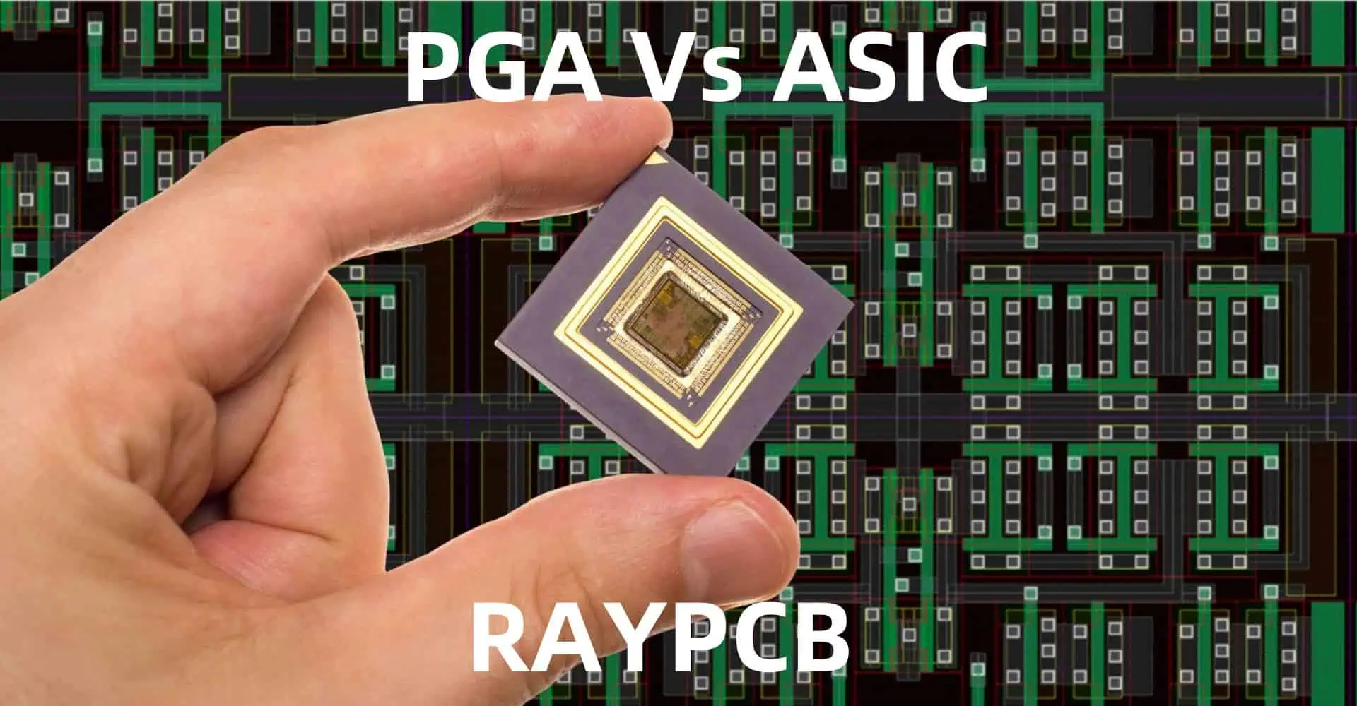
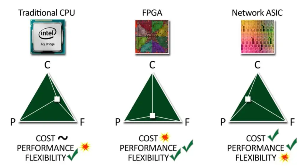
In the world of integrated circuits and digital design, two technologies stand out for their widespread use and distinct characteristics: Field-Programmable Gate Arrays (FPGAs) and Application-Specific Integrated Circuits (ASICs). Both play crucial roles in modern electronics, but they serve different purposes and come with their own sets of advantages and limitations. This article will explore the key differences between FPGAs and ASICs, their applications, and the factors to consider when choosing between them.
Understanding FPGAs
What is an FPGA?
Field-Programmable Gate Arrays (FPGAs) are semiconductor devices that are based around a matrix of configurable logic blocks (CLBs) connected via programmable interconnects. FPGAs can be reprogrammed to desired application or functionality requirements after manufacturing.
An Application-Specific Integrated Circuit (ASIC) is an integrated circuit chip customized for a particular use, rather than intended for general-purpose use. ASICs are designed and manufactured for a specific application or function.
Key Features of ASICs
1. Customization
ASICs are designed for a specific application, allowing for optimized performance, power efficiency, and size.
2. High Performance
Due to their specialized nature, ASICs typically offer higher performance compared to general-purpose chips.
3. Power Efficiency
Custom design allows for optimization of power consumption, making ASICs more energy-efficient for their specific tasks.
4. Cost-Effectiveness for High-Volume Production
While initial costs are high, ASICs become cost-effective in high-volume production scenarios.
ASIC Design Process
The ASIC design process involves several stages:
Specification
Architecture Design
RTL Design
Functional Verification
Logic Synthesis
Physical Design
Timing Analysis
Fabrication
Testing
Applications of ASICs
ASICs are used in a wide range of applications, including:
The decision to use an FPGA or an ASIC depends on various factors. Here’s a decision matrix to help guide the choice:
Factor
FPGA Preferred
ASIC Preferred
Production Volume
Low to Medium
High
Time-to-Market
Critical
Less Critical
Performance Requirements
Moderate
Very High
Power Efficiency
Moderate
Critical
Design Flexibility
High
Low
Budget for Initial Development
Limited
High
Expected Product Lifetime
Short to Medium
Long
Need for Field Updates
Yes
No
Future Trends
As technology continues to evolve, the landscape of FPGAs and ASICs is also changing:
1. Hybrid Solutions
The emergence of hybrid chips that combine FPGA fabric with hard-wired ASIC components is blurring the lines between the two technologies.
2. Advanced Process Nodes
Both FPGAs and ASICs are benefiting from advancements in semiconductor manufacturing, enabling higher performance and lower power consumption.
3. AI and Machine Learning
The rise of AI and machine learning is driving innovation in both FPGA and ASIC design, with specialized architectures emerging for these applications.
4. Open-Source Hardware
The growing open-source hardware movement is making ASIC design more accessible, potentially reducing the cost barrier for custom chip development.
Conclusion
FPGAs and ASICs each have their unique strengths and weaknesses. FPGAs offer unparalleled flexibility and faster time-to-market, making them ideal for rapid prototyping, low to medium volume production, and applications with changing standards. ASICs, on the other hand, provide superior performance, power efficiency, and cost-effectiveness in high-volume production scenarios.
The choice between FPGA and ASIC ultimately depends on the specific requirements of the application, including factors such as production volume, performance needs, power constraints, time-to-market, and budget. As technology continues to advance, we can expect to see further innovations in both FPGA and ASIC technologies, as well as the emergence of hybrid solutions that combine the best of both worlds.
Understanding the differences between FPGAs and ASICs is crucial for engineers, product managers, and decision-makers in the electronics industry. By carefully considering the trade-offs and aligning the choice with project requirements, organizations can optimize their product development processes and deliver innovative solutions to the market.
FAQ
Q1: Can FPGAs be used in high-volume production?
A: While FPGAs are typically more cost-effective for low to medium volume production, they can be used in high-volume production in certain scenarios. This is particularly true when:
The product lifecycle is expected to be short.
The ability to update functionality in the field is crucial.
The performance and power efficiency requirements are not too stringent.
The unit cost difference compared to an ASIC is outweighed by other factors such as time-to-market or flexibility.
However, for very high volume production (typically over 100,000 units), ASICs usually become more cost-effective due to their lower per-unit cost.
Q2: How long does it typically take to develop an ASIC compared to implementing a design on an FPGA?
A: The development time for ASICs and FPGAs can vary significantly:
FPGA: Implementing a design on an FPGA typically takes a few weeks to a few months, depending on the complexity of the design. This includes design, verification, and implementation phases.
ASIC: ASIC development is a much longer process, usually taking 6 to 18 months or even longer for complex designs. This includes stages such as RTL design, verification, logic synthesis, physical design, fabrication, and testing.
The shorter development time for FPGAs is one of their key advantages, allowing for faster time-to-market and easier design iterations.
Q3: Are there any situations where an FPGA might outperform an ASIC?
A: While ASICs generally offer higher performance, there are scenarios where an FPGA might outperform an ASIC:
Rapidly evolving standards: In fields with frequently changing standards or protocols, an FPGA can be updated to support new standards, while an ASIC would become obsolete.
Adaptive algorithms: For applications requiring real-time adaptation of algorithms, FPGAs can be reconfigured on-the-fly, potentially outperforming a fixed-function ASIC.
Parallel processing: Modern FPGAs excel at parallel processing tasks and can sometimes outperform ASICs in specific parallel computing scenarios.
Latest process nodes: High-end FPGAs are often manufactured using the latest process nodes, which might not be economically viable for lower-volume ASIC production.
Q4: How do the power consumption characteristics of FPGAs and ASICs compare?
A: Generally, ASICs are more power-efficient than FPGAs for the same functionality:
Aspect
FPGA
ASIC
Static Power
Higher
Lower
Dynamic Power
Higher
Lower
Power Efficiency
Moderate
High
ASICs consume less power because:
They are optimized for specific functions, eliminating unnecessary circuitry.
They don’t require the programmable interconnects that contribute to power consumption in FPGAs.
Custom design allows for advanced power-saving techniques.
However, the power consumption gap has been narrowing with advancements in FPGA technology. For some low-power applications, modern FPGAs can be competitive with ASICs.
Q5: What are the key considerations for choosing between FPGA and ASIC in terms of long-term cost?
A: When considering long-term costs, several factors come into play:
Production volume: ASICs become more cost-effective at higher volumes, typically beyond 10,000 to 100,000 units, depending on complexity.
Product lifetime: For products with a long lifetime, ASICs can be more cost-effective even at lower volumes due to lower per-unit costs.
Upgrade requirements: If field upgrades are necessary, FPGAs can be more cost-effective as they avoid the need for hardware replacement.
Development costs: ASIC development costs are significantly higher, which must be amortized over the product lifetime.
Power consumption: In applications where power usage has ongoing costs (e.g., data centers), the higher efficiency of ASICs can lead to long-term savings.
Maintenance and obsolescence: FPGAs may have lower long-term costs in rapidly evolving fields due to their adaptability.
A simplified cost comparison over time might look like this:
Time Period
FPGA Cost
ASIC Cost
Initial Development
$100,000
$1,000,000
Per-Unit Cost
$50
$10
10,000 Units
$600,000
$1,100,000
100,000 Units
$5,100,000
$2,000,000
1,000,000 Units
$50,100,000
$11,000,000
These numbers are illustrative and can vary widely based on specific circumstances. It’s crucial to perform a detailed cost analysis based on the specific requirements and lifecycle expectations of your project.
As digital systems continue to push the boundaries of speed and performance, high-speed PCB design has become increasingly complex. Channel Operating Margin (COM) has emerged as a critical metric for ensuring signal integrity and reliable data transmission in high-speed digital designs. This comprehensive guide explores COM analysis, its implementation, and best practices for optimizing high-speed PCB designs.
Understanding Channel Operating Margin
Definition and Fundamentals
Channel Operating Margin represents a unified figure of merit that quantifies the performance and reliability of high-speed serial links. It combines various channel impairments and characteristics into a single numerical value, making it easier for designers to assess link viability. COM is typically expressed in decibels (dB), with higher values indicating better channel performance.
COM calculations involve complex mathematical models that consider both frequency-domain and time-domain analyses. The basic COM equation can be expressed as:
Maintaining consistent impedance throughout the channel is crucial for optimal COM performance. Consider the following target impedances for different applications:
Copper roughness contribution to losses Choose materials with stable Dk and low Df for optimal COM performance.
3. Can COM be improved post-layout without major redesign?
Yes, several techniques can improve COM post-layout:
Optimization of termination values
Fine-tuning of via structures
Local impedance adjustments
Crosstalk reduction through trace spacing adjustments However, major improvements typically require layout modifications.
4. How does temperature affect COM measurements?
Temperature impacts COM through:
Material property changes
Impedance variations
Loss characteristics Design margins should account for the full operating temperature range, typically adding 0.5-1.0 dB margin for temperature effects.
ANSYS SIwave Choose tools that support your specific standard requirements and provide comprehensive analysis capabilities.
Conclusion
Channel Operating Margin remains a crucial metric for high-speed PCB design success. By following the guidelines and optimization strategies outlined in this article, designers can achieve robust and reliable high-speed designs that meet or exceed COM requirements. Continuous monitoring of industry standards and adoption of new technologies will ensure designs remain competitive in the evolving landscape of high-speed digital systems.
In recent years, the industrial sector has witnessed a significant transformation due to the integration of affordable and versatile microcontrollers and single-board computers. Two prominent players in this revolution are Raspberry Pi and Arduino. These compact yet powerful devices have found their way into various industrial applications, offering cost-effective solutions for automation, data acquisition, and process control. This article explores the roles of Raspberry Pi and Arduino in the industrial environment, their strengths and limitations, and how they are reshaping industrial processes.
Understanding Raspberry Pi and Arduino
Raspberry Pi: The Mini Computer
Raspberry Pi is a series of small single-board computers developed by the Raspberry Pi Foundation. Originally designed for educational purposes, it has evolved into a versatile platform for various applications, including industrial use.
Key Features of Raspberry Pi:
Full-fledged computer running Linux-based operating systems
Powerful processors (up to quad-core ARM Cortex-A72)
Arduino is an open-source electronics platform based on easy-to-use hardware and software. It’s designed for creating interactive electronic projects and is widely used in prototyping and small-scale industrial applications.
Comparison: Raspberry Pi vs Arduino in Industrial Settings
To better understand the strengths and weaknesses of Raspberry Pi and Arduino in industrial environments, let’s compare them across several key factors:
Factor
Raspberry Pi
Arduino
Processing Power
High (up to 1.5 GHz quad-core)
Low (16 MHz – 400 MHz)
Operating System
Full OS (Linux-based)
No OS, runs bare-metal code
Memory
512 MB – 8 GB RAM
2 KB – 8 KB SRAM
Storage
MicroSD card (up to 512 GB)
32 KB – 256 KB Flash memory
I/O Capabilities
GPIO pins, USB, HDMI
Analog/Digital pins, limited USB
Networking
Built-in Wi-Fi and Ethernet
Requires additional modules
Real-time Performance
Limited without additional hardware
Excellent
Power Consumption
Higher (2.5W – 6.5W)
Lower (0.1W – 0.5W)
Cost
$35 – $75
$20 – $50
Ease of Programming
More complex (Python, C++, Java)
Simpler (C++, Arduino IDE)
Industrial Applications of Raspberry Pi
1. Data Acquisition and Monitoring Systems
Raspberry Pi’s powerful processing capabilities and networking features make it an excellent choice for data acquisition and monitoring in industrial settings. It can collect data from various sensors, process it in real-time, and transmit it to central servers or cloud platforms.
Example Use Case: Environmental Monitoring in a Manufacturing Plant
The Raspberry Pi’s ability to run a full operating system and support graphical interfaces makes it suitable for creating cost-effective HMI solutions in industrial control systems.
3. Edge Computing and IoT Gateways
In Industry 4.0 applications, Raspberry Pi serves as an excellent platform for edge computing and IoT gateways. It can process data locally, reducing latency and bandwidth requirements while providing a secure interface between local devices and cloud services.
4. Vision Systems and Quality Control
With its processing power and camera module support, Raspberry Pi can be used in machine vision applications for quality control and inspection tasks in manufacturing processes.
Industrial Applications of Arduino
1. Sensor Interfaces and Data Collection
Arduino’s simplicity and extensive sensor library support make it ideal for interfacing with various industrial sensors and collecting data in harsh environments.
Example Use Case: Vibration Monitoring in Industrial Machinery
Arduino’s real-time capabilities and precise timing control make it suitable for small-scale process control and automation tasks in industrial settings.
3. Prototyping and Proof of Concept
The ease of use and low cost of Arduino boards make them excellent tools for rapidly prototyping industrial solutions and creating proof-of-concept models.
4. Embedded Systems in Industrial Products
Arduino’s low power consumption and compact size allow it to be embedded directly into industrial products, enabling smart functionality and data logging capabilities.
While Raspberry Pi and Arduino offer numerous advantages in industrial applications, they also come with certain challenges and limitations that need to be considered:
Raspberry Pi Limitations:
Lack of real-time processing without additional hardware
Potential reliability issues due to the use of SD cards for storage
Higher power consumption compared to microcontrollers
Limited industrial-grade I/O capabilities without expansion boards
Arduino Limitations:
Limited processing power for complex computations
Restricted memory for large-scale data processing
Lack of built-in networking capabilities
Limited multitasking abilities
Best Practices for Industrial Implementation
To maximize the benefits of Raspberry Pi and Arduino in industrial environments, consider the following best practices:
Rugged Enclosures: Use industrial-grade enclosures to protect the devices from dust, moisture, and electromagnetic interference.
Power Management: Implement proper power management solutions, including voltage regulation and backup power systems.
Redundancy: For critical applications, consider implementing redundant systems to ensure reliability.
Security Measures: Implement robust security protocols, especially for networked Raspberry Pi systems, to protect against cyber threats.
Regular Maintenance: Establish a routine maintenance schedule to check for hardware issues, update software, and ensure optimal performance.
Environmental Considerations: Account for temperature, humidity, and vibration levels in the industrial environment when designing solutions.
Case Studies: Successful Industrial Implementations
Case Study 1: Smart Factory Monitoring with Raspberry Pi
A medium-sized manufacturing plant implemented a network of Raspberry Pi devices to monitor various aspects of their production line. The system collected data on machine performance, energy consumption, and environmental conditions.
Results:
Metric
Before Implementation
After Implementation
Improvement
Downtime
120 hours/month
72 hours/month
40% reduction
Energy Consumption
50,000 kWh/month
42,500 kWh/month
15% reduction
Defect Rate
2.5%
1.8%
28% reduction
Case Study 2: Precision Agriculture with Arduino
A large greenhouse operation used Arduino-based systems to control irrigation, monitor soil conditions, and regulate temperature and humidity.
Results:
Metric
Before Implementation
After Implementation
Improvement
Water Usage
1000 m³/week
750 m³/week
25% reduction
Crop Yield
5 tons/acre
6.2 tons/acre
24% increase
Labor Costs
$5000/month
$3750/month
25% reduction
Future Trends and Developments
As industrial applications of Raspberry Pi and Arduino continue to evolve, several trends are emerging:
Integration with AI and Machine Learning: Both platforms are increasingly being used as edge devices for AI-powered industrial solutions.
Enhanced Industrial-grade Versions: Manufacturers are developing more robust, industrial-specific versions of these devices to meet demanding requirements.
Improved Security Features: Future iterations are likely to include enhanced built-in security features to address cybersecurity concerns in industrial settings.
Expanded Ecosystem: The growing ecosystem of compatible sensors, actuators, and expansion boards is making these platforms even more versatile for industrial use.
Conclusion
Raspberry Pi and Arduino have revolutionized the industrial landscape by providing cost-effective, flexible, and powerful solutions for a wide range of applications. While they each have their strengths and limitations, their impact on industrial processes, data acquisition, and automation is undeniable. As these platforms continue to evolve and adapt to industrial needs, we can expect to see even more innovative applications and increased adoption across various sectors of industry.
Frequently Asked Questions (FAQ)
Q: Can Raspberry Pi and Arduino be used in safety-critical industrial applications? A: While both platforms can be used in various industrial applications, they are generally not recommended for safety-critical systems without additional certification and redundancy measures. For such applications, it’s better to use industrial-grade PLCs or certified safety controllers.
Q: How do I choose between Raspberry Pi and Arduino for my industrial project? A: The choice depends on your specific requirements. Use Raspberry Pi for applications requiring more processing power, networking capabilities, or a full operating system. Choose Arduino for projects needing real-time control, low power consumption, or simple sensor interfacing.
Q: Are there industrial-grade versions of Raspberry Pi and Arduino available? A: Yes, there are industrial-grade versions and alternatives available for both platforms. For example, the Raspberry Pi Compute Module is designed for industrial applications, and there are Arduino-compatible boards built to withstand harsh industrial environments.
Q: How can I ensure the reliability of Raspberry Pi and Arduino in 24/7 industrial operations? A: To improve reliability, use industrial-grade power supplies, implement proper cooling solutions, use redundant systems where necessary, and establish regular maintenance routines. Additionally, consider using robust storage solutions for Raspberry Pi, such as industrial-grade eMMC modules instead of SD cards.
Q: What are the main security concerns when using Raspberry Pi or Arduino in industrial settings? A: The main security concerns include unauthorized access to networked devices, potential for data breaches, and vulnerability to malware. To mitigate these risks, implement strong network security measures, use encryption for data transmission, regularly update software and firmware, and restrict physical access to the devices.
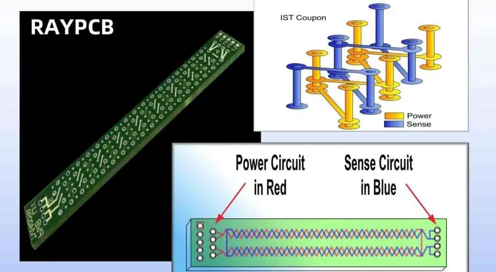
Printed Circuit Boards (PCBs) serve as the backbone of modern electronic devices, providing the essential pathways for electrical signals to travel between components. The interconnect system within a PCB—comprising traces, vias, pads, and other conductive elements—is critical to the board’s functionality. However, various defects can occur during manufacturing, assembly, or operation that compromise these interconnections, leading to performance degradation or complete system failure.
Understanding PCB Interconnect Systems
The interconnect system in a PCB consists of multiple layers of conductive material, typically copper, that form the electrical pathways. These pathways include surface traces that route signals across individual layers, through-hole vias that connect different layers vertically, and pads that provide connection points for components. The complexity of modern PCBs, with their multiple layers and high-density interconnections, makes them susceptible to various types of defects that can affect signal integrity, power distribution, and overall system reliability.
Modern PCBs often feature intricate designs with trace widths measured in micrometers, blind and buried vias, and complex layer stackups. This miniaturization and increased complexity have made interconnect defects more challenging to detect and prevent, requiring sophisticated manufacturing processes and quality control measures.
Categories of Interconnect Defects
Interconnect defects in PCBs can be broadly categorized into manufacturing defects, assembly-related defects, and operational defects that develop over time. Manufacturing defects occur during the PCB fabrication process and include issues such as incomplete etching, poor plating quality, or misaligned layers. Assembly-related defects arise during component mounting and soldering processes, while operational defects develop during the PCB’s service life due to environmental factors, thermal cycling, or mechanical stress.
Manufacturing-Related Interconnect Defects
Open circuits represent one of the most common manufacturing defects, occurring when a conductive path is incomplete or broken. This can result from over-etching during the chemical etching process, where excessive removal of copper creates gaps in traces. Under-etching can cause the opposite problem, where insufficient copper removal leaves unwanted connections between adjacent traces, creating short circuits. These defects are particularly problematic in high-density designs where trace spacing is minimal.
Via defects constitute another significant category of manufacturing issues. Incomplete via plating can create high-resistance connections or complete opens between layers. This occurs when the plating process fails to adequately deposit copper within the via barrel, often due to inadequate cleaning, poor plating solution quality, or insufficient plating time. Void formation within vias can also create reliability issues, as these voids can expand under thermal stress and eventually cause connection failure.
Delamination between layers represents a serious structural defect that can affect interconnect integrity. This occurs when the adhesion between the substrate material and copper layers fails, often due to contamination during manufacturing or inadequate surface preparation. Delamination can lead to intermittent connections and eventual complete failure of the affected interconnects.
Assembly-Related Defects
Solder joint defects significantly impact interconnect reliability, even though they technically occur at the interface between the PCB and mounted components. Cold solder joints, characterized by insufficient heat during soldering, create high-resistance connections that can fail under thermal or mechanical stress. Solder bridges between adjacent pads can create unintended short circuits, while insufficient solder can lead to weak mechanical connections and potential opens.
Pad lifting during assembly represents another critical defect where the copper pad separates from the substrate during soldering or rework processes. This typically occurs due to excessive heat application, multiple rework cycles, or poor pad adhesion. Lifted pads can create complete opens in the interconnect system and are often difficult to repair effectively.
Operational and Environmental Defects
Thermal cycling creates significant stress on PCB interconnects due to the different coefficients of thermal expansion between copper conductors and substrate materials. Repeated expansion and contraction can lead to fatigue cracking in traces and vias, particularly at stress concentration points such as corners or areas where traces change width. This thermal fatigue can progress slowly over time, initially causing intermittent failures before eventually creating complete opens.
Corrosion of copper interconnects can occur in environments with high humidity, salt spray, or chemical exposure. Galvanic corrosion can be particularly problematic when dissimilar metals are present, creating electrochemical cells that accelerate copper dissolution. This corrosion can manifest as surface oxidation, pitting, or complete dissolution of thin traces.
Mechanical stress from vibration, shock, or flexing can cause crack propagation in interconnects. This is especially problematic in applications where PCBs are subject to repeated mechanical loading, such as automotive or aerospace applications. Stress concentrations at via locations or trace corners can accelerate crack initiation and propagation.
Detection and Analysis Methods
Visual inspection remains the first line of defense against interconnect defects, utilizing optical microscopy and automated optical inspection (AOI) systems to detect surface-level defects such as opens, shorts, and dimensional variations. However, many interconnect defects are not visible on the surface and require more sophisticated detection methods.
Electrical testing methods include in-circuit testing (ICT) and flying probe testing to verify connectivity and measure resistance values. These methods can detect opens, shorts, and high-resistance connections but may not identify intermittent defects or those that only manifest under specific conditions.
Cross-sectional analysis involves cutting through the PCB to examine the internal structure of vias and layer interfaces. This destructive testing method provides detailed information about plating quality, void formation, and delamination but can only be performed on sample boards.
Time-domain reflectometry (TDR) and frequency-domain analysis can identify impedance discontinuities and signal integrity issues caused by interconnect defects. These methods are particularly useful for high-speed digital applications where signal integrity is critical.
Prevention and Mitigation Strategies
Design for manufacturability (DFM) principles play a crucial role in preventing interconnect defects. This includes appropriate trace spacing, via sizing, and placement to accommodate manufacturing tolerances. Avoiding sharp corners and providing adequate copper area for thermal dissipation can reduce stress concentrations and improve reliability.
Process control during manufacturing is essential for minimizing defects. This includes maintaining proper etching parameters, ensuring adequate surface preparation for plating, and controlling environmental conditions during assembly. Statistical process control (SPC) methods can help identify process variations before they result in defective products.
Material selection significantly impacts interconnect reliability. Using high-quality substrate materials with appropriate glass transition temperatures and coefficients of thermal expansion can reduce thermal stress. Surface finishes such as immersion gold or organic solderability preservatives (OSP) can protect copper surfaces from oxidation and improve solderability.
Impact on System Performance
Interconnect defects can have varying impacts on system performance depending on their location and severity. Complete opens obviously result in non-functional circuits, while high-resistance connections can cause voltage drops, increased power consumption, and potential timing issues in digital circuits. Intermittent connections can create particularly challenging problems, as they may only manifest under specific operating conditions or environmental stresses.
In high-frequency applications, even minor interconnect defects can significantly impact signal integrity. Impedance discontinuities caused by via defects or trace irregularities can create reflections, crosstalk, and electromagnetic interference. These effects can degrade signal quality and reduce system performance even when the basic connectivity remains intact.
Quality Assurance and Testing
Comprehensive quality assurance programs for PCB interconnects must address both manufacturing and operational aspects. This includes incoming material inspection, in-process monitoring during fabrication, and final testing before shipment. Accelerated life testing under elevated temperature, humidity, and mechanical stress conditions can help identify potential reliability issues before they occur in field applications.
Statistical sampling and failure analysis of returned products provide valuable feedback for improving manufacturing processes and design guidelines. This data can be used to refine quality control procedures and identify emerging failure modes that may require process modifications.
Future Challenges and Considerations
As electronic systems continue to evolve toward higher densities, faster speeds, and smaller form factors, interconnect defects will become increasingly challenging to prevent and detect. Advanced packaging technologies such as embedded components and flexible-rigid constructions introduce new potential failure modes that require updated quality control approaches.
The development of new materials and manufacturing processes offers opportunities to improve interconnect reliability, but also introduces new variables that must be carefully controlled. Continued research into defect mechanisms and prevention strategies will be essential for maintaining the reliability standards expected in modern electronic systems.
Understanding and controlling interconnect defects in PCBs requires a systematic approach that addresses design, manufacturing, and operational factors. Through careful attention to these various aspects, manufacturers can produce reliable PCBs that meet the demanding requirements of modern electronic applications while minimizing the risk of interconnect-related failures.
Printed Circuit Boards (PCBs) are the foundational components of virtually every electronic device, from smartphones and computers to aerospace systems and medical equipment. While the importance of electrical design, component placement, and manufacturing precision in PCB production is well understood, one critical process that often receives less attention but is equally vital is outgassing. This thermal process, which involves the controlled removal of volatile compounds from PCB materials, plays an indispensable role in ensuring the reliability, performance, and longevity of electronic assemblies.
Understanding Outgassing in PCB Context
Outgassing, also known as degassing, is the process by which volatile organic compounds (VOCs), moisture, and other gaseous substances are removed from materials through the application of heat, vacuum, or both. In the context of PCBs, outgassing specifically targets the elimination of these unwanted substances from the various materials that comprise the board, including the substrate, solder mask, silkscreen, and any adhesives or coatings used in the manufacturing process.
The need for outgassing arises from the fundamental nature of PCB materials themselves. Modern PCBs are complex multilayer structures composed of various organic and inorganic materials. The most common substrate material, FR-4 (Flame Retardant 4), is a composite of woven fiberglass cloth impregnated with an epoxy resin. This epoxy resin, along with other polymeric materials used in PCB construction, naturally contains volatile compounds that can be released over time, particularly when exposed to elevated temperatures during operation or subsequent manufacturing processes.
The Science Behind Volatile Compound Presence
The presence of volatile compounds in PCB materials is an inevitable consequence of the manufacturing process itself. During the production of epoxy resins and other polymeric materials, various chemical compounds are used as catalysts, curing agents, flame retardants, and processing aids. Some of these compounds may not fully react during the initial curing process, leaving residual volatile materials trapped within the polymer matrix.
Additionally, environmental factors contribute to the accumulation of volatile compounds. During storage and handling, PCB materials can absorb moisture from the atmosphere. This absorbed moisture, while seemingly innocuous, can cause significant problems during subsequent high-temperature processes such as soldering or component attachment. When heated, this moisture can rapidly expand into steam, creating internal pressure that can lead to delamination, barrel cracking, or other structural failures.
Furthermore, the manufacturing environment itself can introduce contaminants. Dust, oils from handling, residual flux materials, and cleaning solvents can all contribute to the volatile compound burden that must be addressed through proper outgassing procedures.
Critical Applications Requiring Outgassing
The necessity for outgassing becomes particularly pronounced in high-reliability applications where failure is not merely inconvenient but potentially catastrophic. Aerospace and defense electronics represent perhaps the most demanding applications for PCB outgassing. In the vacuum environment of space, any volatile compounds present in PCB materials can be released and subsequently condense on sensitive optical surfaces, solar panels, or other critical components. This contamination can severely degrade the performance of spacecraft systems and potentially jeopardize entire missions.
The aerospace industry has established stringent outgassing requirements, with NASA’s standards being among the most rigorous. These standards typically require that materials exhibit total mass loss of less than 1% and collected volatile condensable materials of less than 0.1% when tested under specified conditions. Meeting these requirements necessitates careful material selection and thorough outgassing procedures during PCB manufacturing.
Medical electronics represent another critical application area where outgassing is essential. Implantable devices, in particular, must meet extremely strict biocompatibility requirements. Any volatile compounds released from PCB materials could potentially interact with biological tissues, causing adverse reactions or device failure. The enclosed nature of many medical devices also means that volatile compounds have limited pathways for escape, making thorough outgassing during manufacturing crucial for long-term reliability.
High-frequency and precision electronics also benefit significantly from outgassing procedures. Volatile compounds can affect the dielectric properties of PCB materials, leading to signal integrity issues, increased loss tangent, and unpredictable electrical performance. In applications such as radar systems, telecommunications equipment, and precision measurement instruments, these effects can compromise system performance and accuracy.
The Outgassing Process and Its Implementation
The outgassing process typically involves exposing PCB materials or completed boards to elevated temperatures for extended periods, often in a controlled atmosphere or vacuum environment. The specific conditions depend on the materials involved and the intended application requirements. Temperatures typically range from 85°C to 150°C, with exposure times varying from several hours to several days.
The process must be carefully controlled to ensure effective volatile compound removal while avoiding damage to the PCB materials or components. Temperature ramping rates are typically controlled to prevent thermal shock, and the atmosphere within the outgassing chamber may be controlled to prevent oxidation or other unwanted chemical reactions.
For bare PCBs, outgassing is often performed before component assembly, allowing for more aggressive treatment conditions. However, populated boards can also be outgassed, though temperature limitations imposed by temperature-sensitive components must be considered. In some cases, selective outgassing of specific areas or components may be necessary.
Benefits Beyond Contamination Control
While contamination control is the primary driver for outgassing requirements, the process provides several additional benefits that contribute to overall PCB reliability and performance. The thermal cycling inherent in outgassing procedures can help identify latent defects in PCB materials or manufacturing processes. Weak bonds, incipient delamination, or other structural issues may become apparent during outgassing, allowing for their identification and correction before final assembly.
Outgassing also contributes to dimensional stability. The removal of volatile compounds and the stress relief that occurs during thermal treatment can reduce the tendency for PCBs to warp or change dimensions during subsequent thermal excursions. This stability is particularly important for fine-pitch components and high-density interconnect applications where dimensional accuracy is critical.
The process can also improve the long-term reliability of solder joints and other interconnections. By removing volatile compounds that could potentially interfere with metallization processes or contribute to corrosion, outgassing helps ensure the integrity of electrical connections throughout the operational life of the device.
Implementation Challenges and Considerations
Despite its benefits, implementing effective outgassing procedures presents several challenges. The process requires specialized equipment capable of maintaining precise temperature and atmospheric control over extended periods. This equipment represents a significant capital investment and requires skilled operators to ensure proper operation.
Scheduling and throughput considerations also present challenges. Outgassing procedures are time-consuming, potentially adding days to the manufacturing cycle. This extended processing time must be balanced against delivery requirements and inventory management considerations.
Material compatibility is another important consideration. While most PCB materials can withstand outgassing conditions, some components or specialized materials may have temperature limitations that restrict outgassing parameters. Careful evaluation of all materials and components is necessary to establish appropriate outgassing conditions.
Quality control and verification present ongoing challenges. Unlike many manufacturing processes where results are immediately apparent, the effectiveness of outgassing procedures may only become evident through long-term testing or in-service performance. Establishing appropriate test methods and acceptance criteria requires careful consideration of application requirements and available testing capabilities.
Future Considerations and Emerging Technologies
As electronic systems continue to evolve toward higher performance, greater miniaturization, and more demanding applications, the importance of outgassing procedures is likely to increase. Emerging technologies such as 3D integrated circuits, advanced packaging techniques, and new materials systems may present unique outgassing challenges that require innovative solutions.
The development of low-outgassing materials represents an ongoing area of research and development. While significant progress has been made in developing materials with reduced volatile compound content, the complete elimination of outgassing requirements remains elusive. Future materials development efforts will likely focus on further reducing volatile compound content while maintaining the mechanical, electrical, and thermal properties required for high-performance applications.
Conclusion
Outgassing represents a critical but often underappreciated aspect of PCB manufacturing and reliability engineering. The controlled removal of volatile compounds from PCB materials is essential for ensuring the long-term reliability and performance of electronic systems, particularly in demanding applications such as aerospace, medical, and high-frequency electronics. While the process presents implementation challenges in terms of equipment requirements, processing time, and quality control, the benefits in terms of contamination control, reliability improvement, and performance optimization make it an indispensable part of high-quality PCB manufacturing.
As electronic systems continue to advance and operate in increasingly challenging environments, the importance of proper outgassing procedures will only continue to grow. Understanding and implementing effective outgassing strategies is therefore essential for any organization involved in the design and manufacture of high-reliability electronic systems.
The printed circuit board (PCB) forms the backbone of virtually every electronic device, making supplier selection and ongoing auditing critical to product success. A systematic supplier audit process protects against quality failures, delivery delays, and compliance risks that can devastate product launches and damage brand reputation.
Preparing for the Audit
Effective PCB supplier auditing begins long before stepping onto the factory floor. Develop a comprehensive audit checklist covering quality systems, manufacturing capabilities, supply chain management, and regulatory compliance. Review the supplier’s certifications, including ISO 9001, IPC standards, and industry-specific requirements like AS9100 for aerospace or ISO 13485 for medical devices.
Gather documentation beforehand, including process flow diagrams, quality manuals, and recent customer audit reports. This preparation enables auditors to focus on verification rather than discovery during the on-site visit.
Quality Management System Assessment
The foundation of any reliable PCB supplier lies in their quality management system (QMS). Examine how they implement design review processes, incoming material inspection, and statistical process control. A mature QMS demonstrates systematic approaches to problem-solving, continuous improvement, and customer satisfaction measurement.
Pay particular attention to their corrective and preventive action (CAPA) system. Review recent CAPA records to understand how effectively they identify root causes and implement lasting solutions. Strong suppliers maintain detailed records and can demonstrate measurable improvements resulting from their CAPA activities.
Manufacturing Capability Evaluation
Modern PCB manufacturing requires sophisticated equipment and precise process control. Assess the supplier’s technical capabilities against your specific requirements, including layer count, via technology, surface finishes, and tolerances. Verify their equipment maintenance programs and calibration procedures for critical measurement tools.
Examine their process documentation and work instructions. Well-documented processes indicate mature manufacturing operations and reduce variability between operators and shifts. Look for evidence of process validation, especially for critical parameters like plating thickness, drill accuracy, and impedance control.
Supply Chain and Material Control
PCB quality depends heavily on incoming materials, from substrate materials to surface finishes and solder masks. Evaluate the supplier’s incoming inspection procedures and their qualification process for sub-suppliers. Understanding their supply chain helps identify potential risks and ensures material traceability.
Review material storage conditions and handling procedures. Moisture-sensitive materials require controlled environments, and proper electrostatic discharge (ESD) protection is essential throughout the manufacturing process. Inadequate material control often manifests as quality issues in finished products.
Testing and Inspection Capabilities
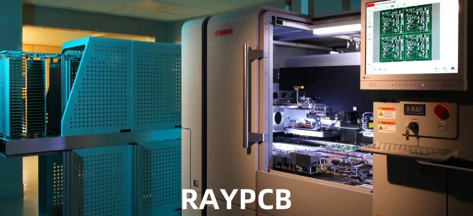
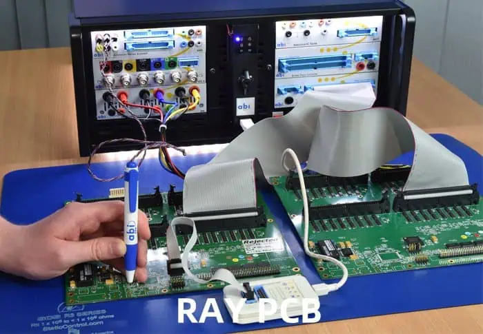
PCB E-test machine
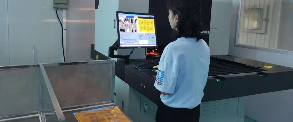
Comprehensive testing separates reliable suppliers from those offering seemingly attractive pricing. Assess their electrical testing capabilities, including in-circuit testing, flying probe testing, and functional testing where applicable. Modern PCB manufacturing should include automated optical inspection (AOI) and automated X-ray inspection for hidden defects.
Evaluate their testing protocols and acceptance criteria. Suppliers should demonstrate statistical sampling plans appropriate for your volume and quality requirements. Review test data retention policies and their ability to provide test results with shipments.
Environmental and Regulatory Compliance
PCB manufacturing involves numerous environmental and regulatory considerations. Verify compliance with RoHS directives, REACH regulations, and conflict minerals reporting requirements. Many applications require additional certifications such as UL recognition or military specifications.
Examine their environmental management systems and waste handling procedures. Responsible suppliers maintain proper permits, conduct regular environmental monitoring, and demonstrate commitment to sustainable manufacturing practices.
Logistics and Communication
Reliable delivery performance requires effective production planning and logistics capabilities. Assess their order management systems, production scheduling processes, and shipping procedures. Understanding their capacity utilization helps predict their ability to meet your delivery requirements, especially during peak demand periods.
Evaluate communication protocols and responsiveness. Effective suppliers provide regular updates on order status, proactively communicate potential issues, and maintain accessible technical support. Language barriers and time zone differences can significantly impact project success.
Financial Stability Assessment
Supplier financial stability affects their ability to invest in equipment, maintain inventory, and weather economic downturns. While detailed financial analysis may require specialized expertise, basic indicators include facility conditions, equipment age, and employee retention rates. Suppliers struggling financially often reduce maintenance, delay equipment upgrades, or experience high turnover rates.
Documentation and Continuous Monitoring
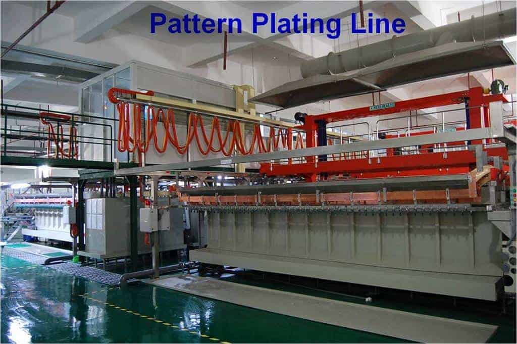
PCB pattern plating line
Document audit findings systematically, including photographic evidence where appropriate. Develop supplier scorecards that track key performance indicators such as on-time delivery, quality metrics, and responsiveness to issues. Regular performance reviews based on actual delivery data provide ongoing insight into supplier capabilities.
Establish clear expectations for improvement plans where deficiencies are identified. Effective suppliers welcome feedback and demonstrate commitment to addressing identified issues within agreed timeframes.
Building Long-term Partnerships
The most successful PCB supplier relationships extend beyond transactional interactions to strategic partnerships. Suppliers invested in your success provide valuable design feedback, suggest cost reduction opportunities, and prioritize your requirements during capacity constraints.
Regular communication, fair payment terms, and reasonable volume commitments encourage suppliers to invest in capabilities that benefit your products. These partnerships often yield innovations and cost savings that purely price-focused relationships cannot achieve.
Conclusion
Thorough PCB supplier auditing requires significant investment in time and expertise, but the cost of supplier failures far exceeds audit expenses. A systematic approach covering quality systems, manufacturing capabilities, compliance, and communication establishes the foundation for reliable supply chain performance.
The audit process should evolve based on experience and changing requirements. Regular reassessment ensures suppliers continue meeting your needs as products and technologies advance. In an increasingly complex electronics landscape, rigorous supplier auditing represents essential risk management and competitive advantage.
Remember that auditing is not a one-time activity but an ongoing process that strengthens supplier relationships and protects product quality. The investment in comprehensive supplier assessment pays dividends through reduced quality issues, improved delivery performance, and enhanced product success in the marketplace.
Printed Circuit Boards (PCBs) operating in harsh environments face numerous challenges that can compromise their functionality, reliability, and lifespan. Understanding which PCB designs, materials, and construction techniques work best under extreme conditions is crucial for applications ranging from aerospace and military systems to industrial automation and automotive electronics. This comprehensive overview examines the key factors that make PCBs suitable for demanding environmental conditions.
Environmental Challenges and Their Impact
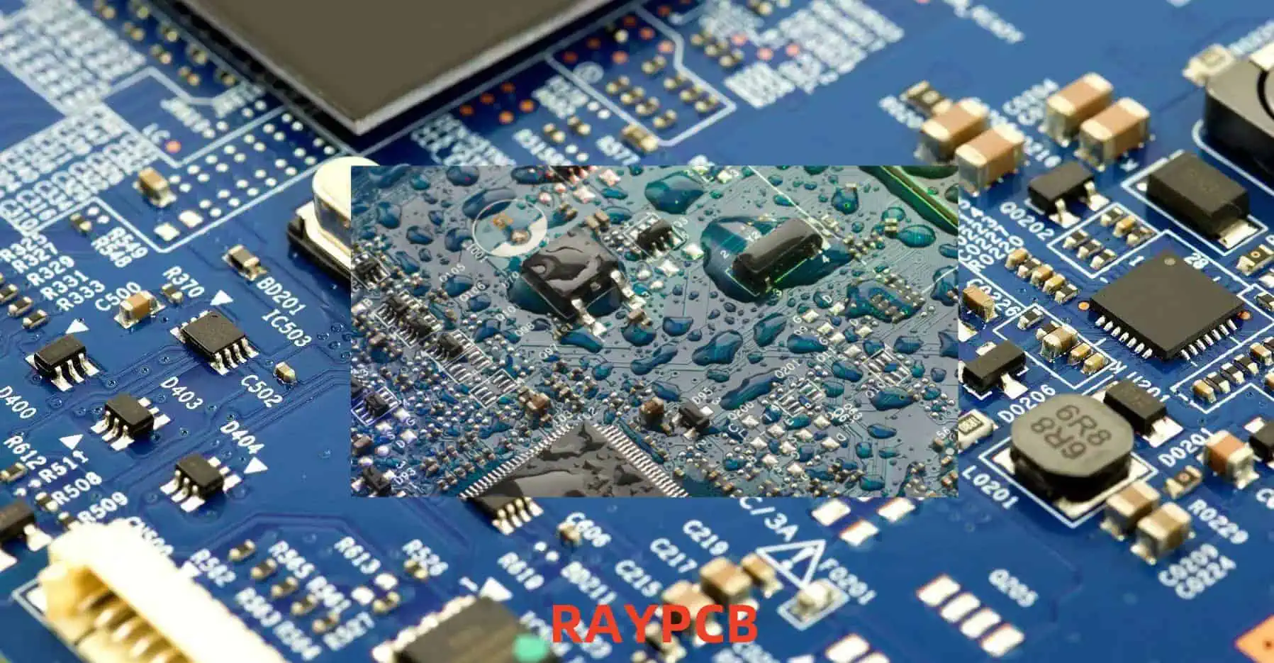
Harsh environments present multiple simultaneous stressors that can degrade PCB performance. Temperature extremes cause thermal expansion and contraction, leading to mechanical stress on solder joints, component packages, and the PCB substrate itself. High humidity and moisture exposure can cause corrosion, delamination, and electrical leakage paths. Chemical exposure from industrial processes, salt spray in marine environments, or corrosive gases can attack copper traces, component leads, and protective coatings.
Mechanical stress from vibration, shock, and acceleration forces can cause solder joint fatigue, component displacement, and PCB flexing that leads to trace cracking. Radiation exposure in space applications or nuclear environments can alter semiconductor characteristics and degrade organic materials. Each of these factors requires specific design considerations and material selections to ensure reliable operation.
High-Temperature PCB Solutions
For applications requiring operation above standard commercial temperature ranges (typically -40°C to +85°C), specialized materials and construction techniques become essential. Polyimide substrates offer excellent thermal stability, maintaining their mechanical and electrical properties at temperatures exceeding 200°C. These flexible and rigid-flex PCBs using polyimide can withstand repeated thermal cycling without delamination or dimensional instability.
Ceramic substrates, particularly aluminum oxide (alumina) and aluminum nitride, provide exceptional thermal performance for extreme high-temperature applications. These materials offer excellent thermal conductivity, low thermal expansion coefficients, and stability at temperatures reaching 300°C or higher. However, ceramic substrates require specialized manufacturing processes and are typically more expensive than traditional FR-4 options.
High-temperature FR-4 variants, designated as Tg (glass transition temperature) materials, offer improved performance over standard FR-4. These materials maintain their structural integrity at elevated temperatures, with some formulations rated for continuous operation at 130°C to 170°C. The selection of appropriate solder alloys becomes critical in high-temperature applications, with lead-based solders generally offering better performance than lead-free alternatives at extreme temperatures.
Moisture and Corrosion Resistance
Protecting PCBs from moisture and corrosive environments requires both material selection and protective coating strategies. Conformal coatings serve as the primary defense against environmental contaminants. Acrylic coatings provide good moisture protection and are easily repairable, while polyurethane coatings offer superior chemical resistance. Silicone coatings excel in extreme temperature applications but may be difficult to remove for repairs.
Parylene coatings, applied through a vapor deposition process, create an extremely thin, pinhole-free protective layer that conforms to complex geometries. This coating type provides excellent moisture and chemical barrier properties while adding minimal thickness or weight to the assembly. For the most demanding applications, multiple coating layers or combination coating systems may be employed.
Substrate selection plays a crucial role in moisture resistance. Traditional FR-4 can absorb moisture, leading to dimensional changes and reduced electrical performance. Low-moisture-absorption materials such as PTFE-based substrates or specialized polyimide formulations maintain stable properties in high-humidity environments. These materials typically exhibit moisture absorption rates below 0.1%, compared to 0.15-0.20% for standard FR-4.
Mechanical Durability and Shock Resistance
PCBs subjected to high levels of vibration, shock, or mechanical stress require robust construction techniques and appropriate material selection. Thicker PCB substrates, typically 1.6mm or greater, provide improved mechanical strength compared to thinner boards. However, this must be balanced against weight and space constraints in many applications.
Component selection and mounting techniques significantly impact mechanical durability. Surface-mount components generally offer better shock and vibration resistance than through-hole components due to their lower mass and profile. However, through-hole mounting may be preferred for larger, heavier components or in applications where repair access is important.
Solder joint reliability becomes critical in mechanically demanding environments. Careful attention to pad design, solder joint geometry, and thermal management helps prevent fatigue failures. The use of underfill materials around critical components provides additional mechanical support and stress distribution. Potting compounds can encapsulate entire PCB assemblies, providing maximum protection against mechanical stress while also offering environmental sealing.
Chemical and Radiation Resistance
Chemical resistance requirements vary widely depending on the specific environment. Industrial process control equipment may encounter acids, bases, solvents, or other reactive chemicals. Marine applications face salt spray and chloride exposure. Selection of appropriate substrate materials, conductor finishes, and protective coatings must consider the specific chemical threats present.
PTFE-based substrates offer excellent chemical inertness but present manufacturing challenges due to their non-adhesive properties. Specialized pretreatment processes or adhesive systems are required to achieve reliable conductor adhesion. Polyimide substrates provide good chemical resistance while maintaining easier manufacturability compared to PTFE materials.
Radiation-hardened PCBs for space or nuclear applications require careful material selection to minimize radiation-induced degradation. Glass-filled epoxy substrates generally show better radiation tolerance than purely organic materials. Metal core PCBs using aluminum or copper substrates can provide improved radiation shielding while also offering superior thermal management.
Advanced Construction Techniques
Embedded component technology places passive components within the PCB substrate layers, reducing profile height and improving mechanical robustness. This technique eliminates traditional solder joints for embedded components, reducing potential failure points in harsh environments. However, embedded components cannot be easily replaced if failures occur.
Metal core PCBs incorporate aluminum or copper substrates to provide superior thermal dissipation and mechanical strength. The metal core acts as both a heat spreader and structural reinforcement, making these boards well-suited for high-power applications in harsh environments. Thermal interface materials between the dielectric layer and metal core optimize heat transfer while maintaining electrical isolation.
Rigid-flex PCB construction combines the mechanical robustness of rigid sections with the flexibility needed for dynamic applications or complex three-dimensional packaging. The flexible sections can absorb mechanical stress that might otherwise damage rigid PCB areas. Proper design of the rigid-flex transitions and appropriate material selection for the flexible sections are critical for long-term reliability.
Testing and Qualification Standards
Validation of harsh environment PCB performance requires comprehensive testing protocols that simulate real-world conditions. Thermal cycling tests evaluate the ability to withstand repeated temperature excursions, typically following standards such as IPC-9701 or MIL-STD-202. These tests identify potential failure modes including solder joint fatigue, delamination, and component package cracking.
Salt spray testing per ASTM B117 evaluates corrosion resistance for marine or industrial applications. Humidity testing following IPC-9693 assesses moisture resistance and insulation properties under high-humidity conditions. Vibration and shock testing per MIL-STD-810 validates mechanical durability under dynamic loading conditions.
Combined environment testing, where multiple stressors are applied simultaneously, provides the most realistic assessment of harsh environment performance. These tests may combine temperature cycling with vibration, humidity exposure with thermal stress, or other combinations relevant to the intended application.
The selection of PCBs for harsh environments requires careful consideration of all environmental factors, application requirements, and cost constraints. Success depends on the integration of appropriate materials, construction techniques, protective measures, and validation testing to ensure reliable operation throughout the intended service life. As electronic systems continue to expand into increasingly demanding applications, the development of more robust PCB technologies remains an active area of research and development.
Line efficiency is a crucial metric in PCB manufacturing that directly impacts productivity, cost-effectiveness, and overall business success. This comprehensive guide explores the various aspects of line efficiency in PCB manufacturing, including measurement methods, optimization strategies, and best practices for maintaining high productivity levels.
Q1: What is the most important factor in maintaining high line efficiency?
A: The most critical factor is maintaining a balanced production line with minimal bottlenecks. This requires careful attention to equipment maintenance, operator training, and process optimization. Regular monitoring of KPIs and quick response to efficiency drops are essential components of maintaining high line efficiency.
Q2: How can setup times be reduced to improve line efficiency?
A: Setup time reduction can be achieved through several methods: implementing SMED (Single-Minute Exchange of Die) techniques, standardizing setup procedures, using quick-change fixtures, maintaining organized workstations, and ensuring all necessary tools and materials are readily available. Proper training and documentation are also crucial.
Q3: What role does preventive maintenance play in line efficiency?
A: Preventive maintenance is crucial for maintaining high line efficiency as it helps prevent unexpected breakdowns and reduces unplanned downtime. A well-planned preventive maintenance schedule can increase equipment reliability, extend machine life, and ensure consistent production quality.
Q4: How does batch size affect line efficiency?
A: Batch size has a significant impact on line efficiency. Larger batches typically result in higher efficiency due to fewer changeovers, but they can also lead to increased inventory costs and reduced flexibility. The optimal batch size should balance setup time, inventory costs, and customer demand requirements.
Q5: What are the key indicators that line efficiency is declining?
A: Key indicators of declining line efficiency include increased cycle times, rising defect rates, more frequent equipment stoppages, increased setup times, and decreased throughput. Regular monitoring of these metrics helps identify efficiency issues before they become serious problems.
Conclusion
Line efficiency in PCB manufacturing is a complex interplay of various factors including equipment performance, process optimization, workforce management, and quality control. Success in maintaining high efficiency levels requires a systematic approach to monitoring, analysis, and continuous improvement. By focusing on key metrics, implementing proper controls, and maintaining a well-trained workforce, PCB manufacturers can achieve and maintain optimal line efficiency levels.
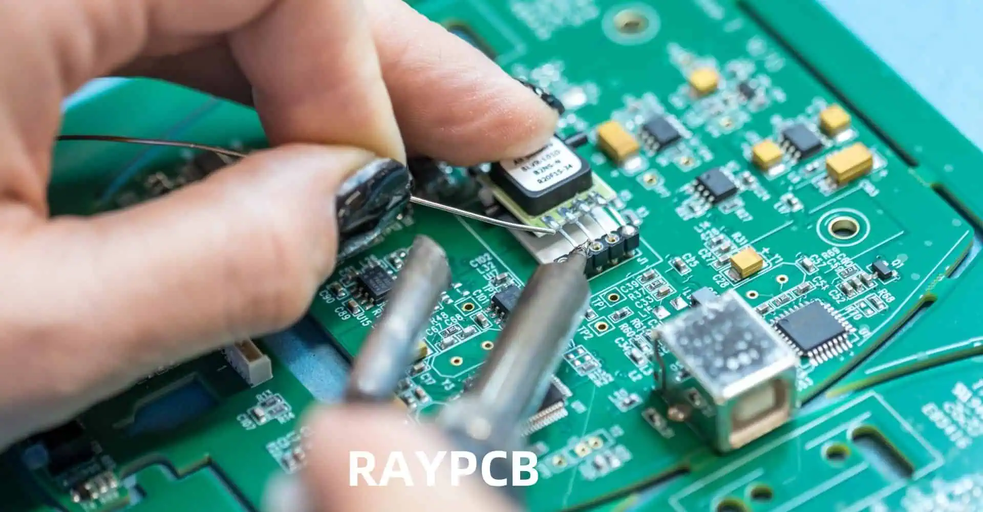
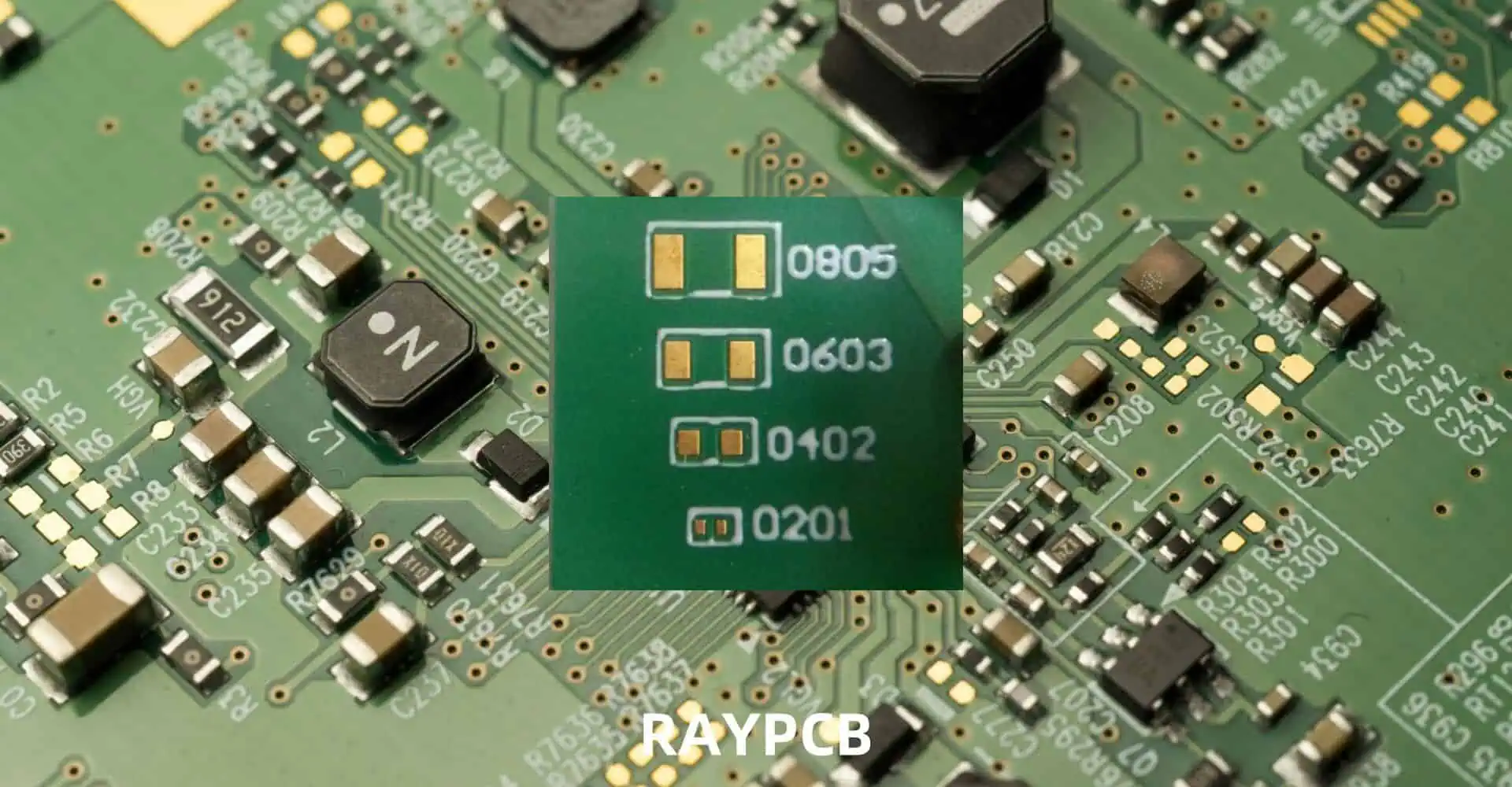
Working with 0201 components and other miniature electronic parts has become increasingly common in modern electronics manufacturing. These ultra-small components, measuring just 0.6 x 0.3 mm (0.024 x 0.012 inches), present unique challenges for handling, placement, and soldering. This comprehensive guide will walk you through everything you need to know about working with these tiny components effectively and reliably.
Understanding 0201 Components
Size Classification
The 0201 designation refers to the imperial measurements of the component: 02 represents 0.02 inches in length, and 01 represents 0.01 inches in width. Here’s a comparison of common SMD component sizes:
Size Code
Imperial (inches)
Metric (mm)
Common Applications
603
0.06 x 0.03
1.6 x 0.8
General purpose electronics
402
0.04 x 0.02
1.0 x 0.5
Mobile devices, wearables
201
0.02 x 0.01
0.6 x 0.3
Smartphones, ultra-compact devices
1005
0.016 x 0.008
0.4 x 0.2
Advanced miniature electronics
Types of 0201 Components
Different types of components are available in the 0201 package size:
Q1: What is the minimum equipment needed to work with 0201 components?
A: The essential equipment includes a stereo microscope (minimum 10x magnification), ESD protection equipment, precision tweezers or vacuum pickup tools, and appropriate soldering equipment with temperature control. A good lighting system is also crucial.
Q2: How can I prevent losing 0201 components during handling?
A: Use proper ESD-safe vacuum pickup tools, work under adequate magnification, maintain a clean and well-lit workspace, and use component presenters or tape feeders. Always handle components over an ESD-safe surface to catch any dropped parts.
Q3: What are the most common defects when soldering 0201 components?
A: The most common defects include tombstoning (component standing on end), solder bridging between pads, insufficient solder joints, and component misalignment. These can be prevented through proper PCB design, correct solder paste application, and controlled reflow profiles.
Q4: Is it possible to hand-solder 0201 components?
A: Yes, but it requires significant skill, proper equipment, and patience. It’s recommended to use a microscope, fine-tip soldering iron with temperature control, and appropriate flux. However, reflow soldering is generally preferred for production volumes.
Q5: What is the recommended storage method for 0201 components?
A: Store components in their original moisture-barrier bags with desiccant and humidity indicators. Use ESD-safe containers in a controlled environment with 40-60% relative humidity. For opened reels, use proper component storage systems with humidity control.
Conclusion
Working with 0201 components requires attention to detail, proper equipment, and well-controlled processes. Success depends on following established guidelines for handling, placement, and soldering while maintaining appropriate quality control measures. As electronics continue to miniaturize, these skills become increasingly valuable in modern electronics manufacturing.