The Shengyi S1190 is another PCB material with high quality. If you knew everything about the Shengyi S1190 PCB material, you would not be here. So we welcome you to learn and gain vast knowledge about the Shengyi S1190 PCB material. We will be discussing its features, properties, and benefits.
The Shengyi S1190 PCB materials have a superior thermal resistance, excellent anti-CAF performance and extremely low coefficient of thermal expansion in the Z-axis. Also, they are very useful in high layer count printed circuit boards. This information we are about to give will be of great help to you. Please continue reading to learn more.
What is Shengyi S1190?
The Shengyi S1190 is a PCB material that offers great qualities. These include its temperature for glass transition at 170 degrees centigrade, its excellent anti-CAF performance, and its great thermal resistance.
Furthermore, its through-hole reliability is excellent. The main application of the Shengyi S1190 is for any high count printed circuit boards
General Properties of the Shengyi S1190 PCB Material
The Shengyi S1190 PCB material has some special properties, which makes them unique. Below are some of them.
Temperature for glass transition (Tg)
The Shengyi S1190 PCB material has a Tg of 170 for the TMA condition. This means that at this temperature, the printed circuit board material will change from the hard stage to the soft one. This property makes it great for use in printed circuit boards. At Tg 170, you are sure that the printed circuit board’s mechanical stability throughout the entire operational life is ensured.
The Tg for Shengyi S1190 PCB material for the DMA condition is 200 degrees centigrade.
Decomposition Temperature (Td)
The Shengyi S1190 and its printed circuit board (Shengyi S1190 PCB) have a decomposition temperature of 350 degrees centigrade. Furthermore, this temperature is one at which the Shengyi S1190 PCB material decomposes chemically. This means the Shengyi S1190 PCB material loses a minimum of 5% of its mass.
Coefficient of Thermal Expansion (Z-axis)
As mentioned earlier, the CTE for the Z-axis is very low. At 50 to 260 degrees centigrade, the value stands at 2.3%. This shows how much the Z axis of the Shengyi S1190 PCB will contract or expand when cooled or heated.
Before the glass transition temperature, the value stands at 45 ppm/℃, while after the glass transition temperature, it stands at 210 ppm/℃.
Thermal Resistance
The Shengyi S1190 PCB material has a high thermal resistance. This means that the Shengyi S1190 PCB has a high ability to resist heat flow. This is one good reason why devices having the Shengyi S1190 PCB material will not experience any damages easily.
The Shengyi S1190 PCB material has a dielectric constant of 4.6 and 4.8 at 1GHz and 1MHz respectively. This frequency plays a huge role in the value. This means that it drops as frequency increases.
Also, this value is significant for impedance considerations and signal integrity. These factors are very significant for electrical performance of high frequency.
Great anti-CAF Performance
The Shengyi S1190 PCB material also has great anti-CAF performance. With this, damages that may happen as a result of oxidation will be prevented. With this property, you can be sure that the product’s durability will be increased.
Storage Conditions for the Shengyi S1190 PCB Material
When the Shengyi S1190 multilayer pcb material is 3 months, you should store it at a maximum temperature of 23 degrees centigrade. Also, storage should be at a relative humidity of less than 50%.
Furthermore, when the Shengyi S1190 PCB material is 6 months, you should store it at a maximum temperature of 5 degrees centigrade. Note that, before you use it, you have to normalize it at room temperature for a minimum of four hours.
Also, be very careful of moisture and wrap it using a damp-proof material. Always keep it in a normal condition. This is because the prepreg may end up absorbing moisture, leading to the weakening of its bonding strength.
Furthermore, during storage, avoid ultraviolet rays as well as any strong light.
Applications of the Shengyi S1190 PCB Material
There are lots of applications, which need high temperatures when operating them. When making use of these applications, you should consider making use of the Shengyi S1190 PCB material.
Here are some applications where the Shengyi S1190 PCB material is useful
Computer Applications
There have been great advancements in the technological world today, which has a great impact on computers under any high temperature. This is why any computer having the Shengyi S1190 PCB material can handle high temperature conditions.
Equipment for communication
Remember that most communication infrastructures pass via heat of high temperatures. This is why it is important that printed circuit boards of Shengyi S1190 PCB material are present in equipment. This helps in enhancing its performance.
High-layer count PCB
The Shengyi S1190 PCB material is also useful in high-layer count printed circuit boards. This type of printed circuit board is seen in weather analysis, satellite systems, medical equipment, GPS technology, data storage, file servers, and more.
What are the Benefits of the Shengyi S1190 PCB Material?
The Shengyi S1190 PCB material has a great advantage. This has to do with its relevance due to its high Tg. One great benefit of using this material is its stability. Other benefits of the Shengyi S1190 PCB material are highlighted below.
Shengyi S1190 PCB material possesses excellent heat dissipation. This means you have nothing to worry about when it comes to heat burdens.
Great Processability
It is very easy to process Shengyi S1190 PCB material. This is because of its high Tg at 170. Processability becomes simple because of its closeness to the best possible temperatures necessary for processing.
Conclusion
The Shengyi S1190 PCB material has lots of great properties and we hope we were able to satisfy your expectations as regards the topic. As mentioned in the article, it has great thermal resistance, great anti-CAF performance, and very low coefficient of thermal expansion at the Z-axis. If you have any questions, feel free to ask us here.
Printed circuit boards (PCBs) are essential components in all electronic devices and equipment. The United Kingdom has a robust PCB industry supplying original equipment manufacturers (OEMs) across many sectors. This article profiles the 10 leading PCB manufacturing and assembly companies in the UK supporting domestic and international customers with advanced capabilities and services.
Overview of UK PCB Industry
Key facts about PCB manufacturing and assembly in the United Kingdom:
Industry generates over £1 billion in annual revenues
Employs more than 13,000 people
Home to ~120 active PCB companies
Major clusters near London, Scotland, and Northern England
Supplies diverse markets including automotive, aerospace, industrial, medical, communications, defense, instrumentation and more
Leading UK PCB companies compete globally and export worldwide
With advanced technological infrastructure and engineering resources, the UK provides full-service prototype through production PCB solutions. We examine the top players in this essential industry.
MOS focuses on responsive, high-mix assembly production.
Conclusion
The United Kingdom possesses strong PCB manufacturing and assembly capabilities supporting diverse industries. Companies like Futurrex, TT Electronics, Primary Circuits, and others highlighted here offer advanced technologies, experience, and reliability serving domestic and overseas customers. The UK remains strategic for cost-effective, high-quality PCB solutions.
Frequently Asked Questions
What are the major PCB technology capabilities found in the UK?
What industries are served by UK PCB manufacturers?
Major industry sectors supported include defense, aerospace, space, automotive, rail, medical devices, industrial equipment, electronics, instrumentation, communications, and more.
Do UK companies focus on prototypes or production?
Leading UK PCB companies offer the full range of services from quick-turn prototypes to high-volume production and everything in between. Vertically integrated providers are common.
Are UK PCB companies competitive globally?
Yes, many UK providers export products worldwide. They offer technical capabilities and certifications on par with top PCB manufacturers in other countries thanks to advanced facilities and engineering expertise.
Why choose a UK PCB partner over low-cost locations?
Benefits include proximity, IP protection, responsive delivery, engineering collaboration, compliance with UK/EU standards, supply chain logistics, and access to funding and R&D support. The UK offers an optimal blend of capabilities, infrastructure, and ecosystems.
Shengyi has been producing PCB laminates for a while now. This company has produced several kinds of laminates. The Autolad1 is one of Shengyi’s products. In this article, we will shed more light on Shengyi Autolad1 PCB material
What is Shengyi Autolad1?
Autolad1 is a mid-Tg lead-free laminate specifically designed for high-performance applications. This PCB material is environmentally friendly since it contains no lead. Also, Shengyi Autolad1 is a PCB material widely used in the automotive industry.
In addition, this PCB material features great ant-CAF performance. This PCB material is specifically designed for automotive electronics like ECU and junction box.
Shengyi Autolad1 has a water absorption rate of 0.09%. This is very low. Therefore, this PCB material can withstand moisture conditions.
Moderate glass transition temperature (Tg)
The glass transition temperature of Autolad1 is 165 degrees Celsius at DMA. Also, the Tg at DSC is 156 degrees Celsius. Therefore, the Tg of this PCB material is moderate. This means that this PCB material can’t operate beyond 165 degrees Celsius.
High Decomposition temperature (Td)
The Td of Shengyi Autolad1 is 353 degrees Celsius at 5% weight loss. The decomposition temperature of a PCB material specifies the temperature at which Autolad1 chemically decomposes. Autolad1 features a high decomposition temperature which is ideal for PCB fabrication.
Low coefficient of thermal expansion (CTE)
The coefficient of thermal expansion on the Z axis is 37ppm/℃. Therefore, this CTE value is very low. CTE measures the rate at which a PCB material expands as heat increases. Also, as the temperature of a material increases beyond Tg, the CTE value will increase. The CTE of Autolad1 after Tg is 210ppm/℃.
Thermal stress
The thermal stress of Autolad1 is >100 at 288 degrees Celsius. Basically, thermal stress specifies mechanical stress as a result of change in a material’s temperature.
Low loss tangent
The loss tangent of Autolad1 is 0.0145. This is very low. Also, the loss tangent measures the power or signal loss of Autolad1. It measures signal los as a result of electromagnetic energy dissipation in the PCB.
Autolad1 is RoHS compliant since it is lead free. Therefore, this PCB material is ideal for fabricating different kinds of circuit boards.
Anti-CAF performance
Conductive Anodic Filament (CAF) is a major concern in electronic production. Also, CAF is a metallic filament created from an electrochemical movement process. Therefore, Shengyi Autolad1 PCB material is resistant to CAF.
Great thermal performance
Shengyi Autolad1 features excellent thermal properties like moderate Tg and low CTE. Also, it features a high decomposition temperature. All of these properties contribute to the thermal performance of Shengyi Autolad1.
Ideal for lead free reflow process
Shengyi Autolad1 is suitable for the lead free reflow process.
The Impact of Glass Transition Temperature on Shengyi Autolad1
Shengyi Autolad1 PCB material features a glass transition temperature of 165 degrees Celsius. This value is close to the high Tg group. Therefore, if the temperature rises beyond this point, the material becomes runner-like. Also, materials featuring high Tg can’t burn. Autolad1 features greater stability due to its moderate Tg.
Also, Shengyi Autolad1 is ideal for multilayer PCB. This is because of its moderate Tg. Autolad1 provides great heat dissipation due to its moderate Tg. Also, this material can prevent electric currents leakage. In addition, this PCB material is easier to process. This is as a result of its Tg value.
The processing of Autolad1 involves several steps. Here are guidelines to help you carry out the Autolad1 processing successfully.
Panel cutting
Here, the manufacturer uses shearing and sewing methods. Avoid possible edge cracks when utilizing roller cutters.
Thin core baking
This depends on specific needs. It is advisable to rinse cutting panels. This helps to get rid of the resin powder caused by cutting. Also, it helps to prevent etching issues. The baking condition should be around 150 degrees Celsius/4-8h.
Lay-up
You need to be certain of the prepreg direction of warp. Also, avoid any prepreg overturn or reversal in case of multilayer PCB distortion after press.
Press process
It is ideal to maintain a heat up rate at 1.0-2.5 degree Celsius per min when material temperature ranges from 80 to 140 degrees Celsius. Set full pressure between 300-420 PSI. Also, apply full pressure only when the top layer temperature is between 80-100 degrees Celsius.
Drilling
As Autolad1 becomes a bit harder, drilling efficiency is important. Also, this helps to ensure hole quality. Reduce the hit count and chip load.
Desmear
Autolad1 is a filled resin system. Therefore, it is harder to desmear than traditional FR4. It is advisable to strengthen the desmear and utilize ultrasonic rinse. Baking after drilling can enhance the effect of desmear.
Soldermask
Avoid warpage or panel distortion due to improper stack-up at the baking process.
HAL
Autolad1 is ideal for lead free HAL process. If there is any measling, bake at 150°C/2-4h.
Packaging
Before packaging, bake finish boards at 125°C/4-6h. Therefore, this will prevent the effect of moisture on the heat resistance of Autolad1. Warp the material by an aluminum pack if stored for a while.
Storage and Packaging Guidelines for Shengyi Autolad1
It is important to store the Shengyi Autolad1 in a good condition. Keep this PCB material in a proper pallet. Also, avoid heavy pressure.
Keep Autolad1 at ambient and ventilated conditions. Also, avoid exposing the material to the elements.
The shelf life of single sided laminate is one year. For double sided, it is two years when kept in proper storage conditions.
Slippage and collision can damage the cladding copper. Therefore, wear clean gloves when handling Autolad1. Also, naked hand can contaminate the cladding copper surface.
Place prepreg horizontally. Also, use a plastic film to reseal any remaining prepreg.
Store all prepreg at below conditions after receiving packaging. Watch out for relative humidity since it has a negative impact on prepreg properties.
Conclusion
Shengyi Autolad1 PCB material is specifically designed to meet the demands of the automotive industry. This PCB material has great properties and advantages. This article has provided in-depth information about Shengyi Autolad1 PCB material.
Sometimes what you need is a little bit more than just epoxy. That’s why Arlon 55NT manufactures both epoxy and aramid laminates and prepreg. What’s the difference?
Epoxy is an adhesive commonly used to create a tough, durable surface for aircraft or other vehicles. We make Epoxies by mixing two different types of material under high pressure for the combined materials to form a thick liquid. Then we form it into a layer and allow it to harden (sometimes over several days). Its strength comes from how well it bonds various objects. One of the reasons aramid laminates are so popular is because they consist of a polymer called aramid. It has excellent tensile strength and high elongation. We use it as an industrial strengthening material for many years. We can also use it to make composite materials such as body armor.
Lately, Rayming PCB & Assembly have been combining the properties of epoxies and aramids. This helps to strengthen their products. We lay the layers onto each other to create stronger parts or coatings that are impossible with other products. These laminates can form into complex shapes and provide exciting properties.
The word “prepreg” is short for “preform,” meaning a prototype. When a firm creates a prototype, it usually needs to make the product in several pieces. We then fit them together to make one complete model. Finally, the “preform” is cut and shaped into the model so that we can assemble it with minimal material waste. This also allows the company to test out different parts at once. Also, they check how they work with each other without waiting for their manufacture.
The Arlon 55NT epoxy and aramid laminates are a product of the same technology. The main difference is in the resin, which we use to strengthen the laminate. The epoxies usually use a combination of resins called polyphenethylenesulfides (PPS). As a result, they form hard films that can withstand a wide range of temperatures. These are also known as cross-linked polyphenylene sulfides (XPS). However, due to environmental concerns, they no longer manufacture them in large quantities.
Chemical Family:
Epoxy & Epoxy Derivatives is the chemical family that includes:
Polyphenylenesulfide is a chemical that does not contain nitrogen. Instead, it is a polymer made from phenyl groups connected to carbon atoms, with sulfide groups attached to each phenyl group. We can form PPS into various shapes, and it is often helpful as a surface coating on items like aircraft.
In addition to the uses mentioned above, PPS has many other applications. For example, it can help as a barrier material in medicine. They also work as insulation in textiles or as an adhesive material in cosmetics and personal care products. PPS is also effective for closing cellulose triacetate film tubes. This is because of its stiffness and good chemical resistance.
Composite Materials Functions:
Arlon 55NT manufactures prepreg as well as epoxy and aramid laminates. Prepreg is a laminate made of unidirectional fabric impregnated with resin. Arlon 55NT can produce a wide range of prepregs using the same manufacturing technology. Then they process them to create epoxy and aramid laminates. The difference is in the resin (the material used to strengthen the lamination).
Product Families:
The basic resin used in prepregs is polyester. However, Arlon 55NT can also make prepregs with other resins as needed.
Forms:
Preforms are strong and hard. They are polyester that you impregnate with resin, which is then dried under high pressure so that the resin stays in place. When the material reaches room temperature, it shrinks and becomes one solid piece that is extremely hard to break or damage. The finished preform is ready for use as a coating. For example, they use it to coat an aircraft wing or other vehicle parts.
Reinforcement Material:
The Kevlar (Aramid) prepreg consists of a very strong material that is easy to cut and bend but not as easy to tear or break. This is the most used prepreg because we can form it into complex shapes.
Technologies:
The preform is formed by layering and rolling the fabric together. Next, we heat each textile layer to a high temperature and press under extremely high pressure. The pressure and heat combine to form the resin, which hardens into a strong and tough material that we can cut and shape easily by hand.
All Arlon 55NT laminates and prepregs have similar mechanical properties. A composition of resin and cloth forms a laminate with relatively high strength. However, we can rapidly cut it using hand tools.
Mechanical Properties
1. Tensile Strength:
The strength of the laminate is dependent on several factors. It includes the resin composition, the type and amount of cloth used in the laminate, and how well the layers bond together. When properly bonded together, each layer has a 50% tensile strength. When we laminate two layers together, they have a 40% tensile strength. We can find these values on any product datasheet.
2. Flexural Strength:
These tests are usually done on 10–20 cm long samples to simulate a cross-section of the product. Flexural strength can resist bending, such as when a bike frame or an airplane wing bends while under pressure. The no-load strength is the maximum force (in N/mm) that a material can withstand under bending stress before it fails. It measures how much a material can bend and remain unbroken. Compression stress on the laminate has little effect on flexural strength.
3. Young’s Modulus:
Young’s modulus is a value that measures stiffness. It relates to tensile strength and flexural strength. It is often used in aircraft design to indicate how strong the material will be after bending it into an airfoil.
4. Peel Strength to Copper:
This measures how well the laminate will resist shear force. This is when we apply pressure to one side of the laminate against an object like copper. The peel strength to copper depends on the thickness of the lamination, the amount and type of cloth used, and the layers it has.
5. Shear Strength:
Shear strength and peel strength measure how well a material resists stretching. Similar to flexural strength, we can do shear tests on samples about 10–20 cm long to simulate a cross-section of the finished product.
Physical Properties
1. Water Absorption (0.062%):
Water absorption is the amount absorbed into the material in an air-dry setting for at least 12 hours. It measures how much moisture a lamination can absorb before it affects the strength and performance of the material.
2. Specific Gravity:
It measures the density of a material. Specific gravity is the ratio of weight to volume, and it indicates how dense or low the density of a material is. We measure it either with a hydrometer or an electronic balance.
This property measures how well heat can travel from one side of a laminate to the other. We measure it with a commercial infrared thermometer. It simulates heat moves along with the lamination under different temperatures and laminates. Infrared thermometers provide an accurate reading of the feet’ temperature. Therefore, it is essential for aircraft design.
2. Tg:
It measures the amount of heat (in degrees Celsius) needed to evaporate a layer of resin applied in an air-dry setting to form a laminate. Tg also measures how fast the material loses its properties when it reaches certain temperatures.
3. Tm:
Tm is the temperature at which a material loses its strength when exposed to water for long periods.
Arc resistance measures how well a material conducts electricity. We measure it with a UV light that simulates how electricity moves through the material in different temperatures.
Dielectric constant measures a material’s ability to store an electric charge. When we place materials between two conductors, copper and plastic, they can store an electrical charge. It releases it simultaneously under alternating current (AC). This constant measures how the material can store much energy while remaining microscopic. A higher dielectric constant means that we can store more energy in the material during AC discharges.
3. Electrical Strength:
Electrical strength measures the amount of charge stored in a material by a capacitor. Different materials have different electrical strengths. We measure this using an electrostatic generator on the bottom side of the laminate under alternating current.
Conclusion
Finally, these two items are different in scale, meaning the material and thickness. Prepreg is much thinner than an aramid film and much heavier than epoxy. Arlon 55NT has been exploring ways to bring these two types of materials better together.
The FR2 PCB is the most recent in a series of boards from the PCB era used by Rayming PCB & Assembly. The design is a lot more complicated than previous designs, and it requires a lot of fine-tuning to get perfect. It also requires 90% less solder by weight. To design this board, you will need to use new software like EagleCad or OrCAD.
This article will take an in-depth look at what you need to do when designing the FR2 PCB using EagleCad and OrCAD. It includes tips on generating your Gerber files correctly to be 3D printed properly. The guide also discusses making sure you set up your board perfectly. As a result, it makes errors less likely to occur during manufacturing.
The FR2 PCB design consists of many layers, and the FR2 design process is a lot more complicated than other boards. Therefore, to make your life easier, this article will take an in-depth look at the following:
Understanding why the FR2 PCB has so many problems to fix and what you need to do. Testing your board for errors. Doing a physical check for errors. Creating your Gerber files for manufacturing. Making sure any down-hole drill holes have the proper size. So, they don’t cause shorts on your board. Cleaning up the solder mask layer to ensure it is not too thick or too thin could damage components and cause shorts in the future. Fixing misaligned parts of your board.
What is the FR2 PCB?
The FR2 PCB is among the most recent in many boards from the PCB era. Unfortunately, the design proved too complicated, so they removed parts and others to simplify it. The design also has other problems that need fixing before manufacturing. So, this article will go over how to fix them using EagleCad and OrCAD.
Why does it have so many problems?
Most of the problems with this board come from its complex layers and structures. For example, there are a lot of rectangular holes that you will have a hard time making correctly with your etchant. You will have to work harder than with a simpler board to fix these problems.
There are also many tabs for many layers, which adds extra steps to manufacturing because we must cut these tabs before adding the pads and vias. Getting the tabs cut in the correct configuration and position is tricky since they must fit into a small area. A single mistake could cause you to waste time cutting them out correctly and very likely ruin your board.
It’s official: PCBs have bugs, and it’s impossible to fix all of them. As a result, some errors will always slip through the cracks, even with the best equipment and software. To make sure your board is not full of errors, you need to do a lot of testing after designing it.
One way to test for errors is to do a final burn-in test (FBT) before manufacturing. It simulates several months’ use by connecting your board to a computer. Then, you can either buy an expensive burner-test unit or design one yourself using a breadboard and jumper wires.
Conversely, you can create a “functional” test (FT) using OrCAD. Then, you can test how well your board would function if real-world engineers used it. For example, an FT might test if your board functions ideally when you connect the reset pin to a 5V line or max it out to 12V.
Checking for physical errors/problems
Besides doing FBT and FTs on your board, you will also need to check it for errors physically. We cannot detect some defects cannot by FBTs and FTs, such as shorts, which can severely damage a board during manufacturing. You will need to use an electron microscope or a flat-bed scanner with ARES software installed to find these problems.
Creating your Gerber files
As you can see, designing the FR2 PCB is not easy, and it will cost you quite a bit of time and money to get it right.
Fortunately, EagleCad has options that make generating your Gerber files very easy. For example, to create your Gerber files, you need to do the following:
First, set your design up as normal. Then go File > Plot. In the “Plot Job” dialog box, ensure that you select Gerber-2-Gerber. Also, ensure that you check all layers. To do this, uncheck all layers on the left of your screen and then check them until they appear on the right). Finally, when you are happy with your selections, click OK to generate them.
After creating your Gerber files, you must check them for errors using Gimp Gnome or another image editor like Photoshop. Many errors can occur, such as a large square of metal on your board and missing holes on your vias.
Make sure all holes have the proper size for the drill bit you’re using
The drill bit used for drilling down into polypropylene will require different hole diameters. This helps to prevent the drill bit from overheating and melting the plastic. If you do not specify these hole sizes, then whatever we use will have copper dust. Don’t tear your PCB apart to fix this issue!
When creating your Gerber files, you should make sure that you specify the drill diameter for all of your down-hole holes. In EagleCad, the hole property is under the “StdHole” node’s general properties tab. Type the desired drilling diameter (in inches) into “Drill Diameter,” and all of your down-hole holes will have the proper size. You must make sure that every drill hole has an appropriate diameter and that they are consistent. Otherwise, a thin layer of copper will form between them and create shorts on your board.
Fixing problems with your bottom and top ground planes
Due to its tall and wide shape, the FR2 will be very difficult to drill down properly. The topmost layer of the board is extremely fragile. So, it is essential to make sure that all holes go down into this layer before drilling down into the polypropylene.
When drilling down in FR2, you should always use copper tape on the bottom (and not just any copper tape). Otherwise, you risk breaking your board. The other reason to use copper tape is that it helps keep a hole from cracking as soon as you insert it into the hole. In some cases, one inch of tape won’t be enough, and you may need two inches or more.
Entering your Gerber files into the Gerber2PLUS PCB layout software
This is the easy part. Once you have your Gerber files in a readable format, they can be easily imported into any PCB layout software together with a backplane. This will be an isolation pad. With this information, you can easily create your FR2 PCB and ensure everything has the correct wiring.
Conclusion
The FR2 is a very cryptic design, and it is frustrating to build. On top of that, it’s not the easiest board to build because there are so many pieces. As a result, it’s a challenge for experienced engineers to create. However, it’s also an excellent project for students to get their first experience with microcontrollers.
Ohm’s law forms the basis for analyzing electrical circuits. It defines the relationship between voltage, current, and resistance. This fundamental law connects the most important circuit quantities used by electrical engineers and physicists.
Georg Simon Ohm first experimentally determined the law in the 1820s. It is a key principle underlying electronic devices, electrical power systems, sensors, and other applications. Understanding Ohm’s law is essential for circuit design and troubleshooting.
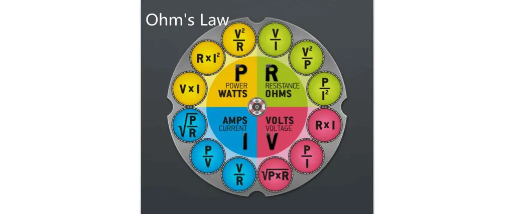
Ohm’s Law Definition
Ohm’s law states that the current (I) flowing through a conductor is directly proportional to the potential difference or voltage (V) applied across it, for any given temperature. The constant of proportionality is called the resistance (R) of the conductor.
Mathematical Formula
The standard mathematical formula for Ohm’s law is:
V = I \cdot R
Where:
V is the voltage in volts (V)
I is the current in amperes (A)
R is the resistance in ohms (Ω)
This simple equation allows calculating any one quantity when the other two are known. The voltage and current follow a linear relationship determined by the resistance.
The standard circuit used to illustrate Ohm’s law consists of a voltage source, conductive path, and ammeter. This setup was used in Georg Ohm’s lab experiments on current flow.
The voltage source (V) applies potential difference across the circuit. This represents the electromotive force driving current.
The conductive path provides a resistance (R). In the diagram, this is a resistor symbol but could be any passive or active load.
An ammeter (A) measures the resulting current through the circuit in amperes.
By adjusting the voltage source and measuring current, the resistance R can be empirically determined from the I/V ratio. This simple circuit provides the foundation for understanding Ohm’s law.
Deriving Ohm’s Law
While Ohm’s law was initially determined experimentally, it can also be derived mathematically based on the principles of electricity and magnetism. Two key equations are used:
Joule’s First Law
Joule’s first law relates the power generated by electric current flowing through a conductor. The power (P) is equal to the current (I) multiplied by the voltage (V):
P = I \cdot V
Where power is measured in Watts (W).
Power-Resistance Relationship
Electric power passing through a resistor converts to heat. The power dissipated this way depends on the resistance (R) and current squared:
P = I^2 \cdot R
By setting the two power equations equal and rearranging terms, Ohm’s law can be derived:
I \cdot V = I^2 \cdot R\\ V = I \cdot R
Therefore, the voltage equals the product of current and resistance, as originally stated by Ohm. This demonstrates Ohm’s law based on the mathematics of power and resistance.
Ohm’s Law Circuit Analysis
Ohm’s law allows analyzing any linear electrical circuit where current flow obeys the I-V-R relationship. Common circuit analysis applications include:
Calculating Current
Use Ohm’s law to calculate the circuit current when voltage and resistance are known:
V = 10 \text{ V}, R = 5 \Omega\\ I = \frac{V}{R}=\frac{10 \text{ V}}{5 \Omega}= 2 \text{ A}
Calculating Resistance
Determine an unknown resistance given voltage and current measurements:
V = 120 \text{ V}, I = 0.5 \text{ A}\\ R = \frac{V}{I}=\frac{120 \text{ V}}{0.5 \text{ A}}= 240 \Omega
Calculating Power
Use Ohm’s law to find the power dissipated by a resistor:
V = 12 \text{ V}, I = 3 \text{ A}\\ P = I^2R = (3 \text{ A})^2(12 \text{ V}) = 108 \text{ W}
Kirchhoff’s Voltage Law
Ohm’s law applied in conjunction with Kirchhoff’s voltage law determines voltages in complex circuits. The sum of voltage rises and drops around any closed loop must equal zero:
V_1 - V_2 + V_3 - V_4 = 0
Where the individual voltages can be found using Ohm’s law.
These examples demonstrate using Ohm’s law to perform critical circuit calculations. The simple V = IR formula is applied to determine unknown quantities.
Ohm’s Law Equation Variations
While the standard equation for Ohm’s law is V = IR, there are two other useful variations:
Current Form
I = \frac{V}{R}
This form directly calculates current when voltage and resistance are known.
Resistance Form
R = \frac{V}{I}
Solves for an unknown resistance given measured values of voltage and current.
Additionally, the power relationship can be substituted:
P = \frac{V^2}{R} = I^2R
So the full set of useful Ohm’s law equations are:
V = IR I = \frac{V}{R} R = \frac{V}{I} P = \frac{V^2}{R} = I^2R
These different forms allow flexibility in applying Ohm’s law to determine any unknown circuit quantity.
Graphing Ohm’s Law
The linear Ohm’s law relationship between current and voltage can be readily graphed:
The slope of the I-V graph is equal to the reciprocal of resistance (1/R). For any given resistor, increasing the voltage results in a proportional increase in current.
Key points from the Ohm’s law graph:
Linear I-V relationship
Slope = 1/R
Intercepts at 0,0
Straight line through origin
Constant resistance for fixed R
Current increases with voltage
This visualization conveys the fundamental Ohm’s law behavior in an intuitive format. The graph can be experimentally generated by measuring current over a range of applied voltages.
Resistance Variance
Georg Ohm’s original law stated that resistance is constant for a uniform conductor at a fixed temperature. However, this is a simplification. Resistance can vary with several factors:
Conductor Shape/Size
Resistance depends on the conductor’s physical dimensions:
R =\rho \frac{L}{A}
Where ρ is resistivity, L is length, A is cross-sectional area.
For a given material, increasing length or decreasing area raises resistance. Resistance is not constant with shape.
Temperature
Metals have a positive temperature coefficient – their resistance increases with temperature. This relationship is approximately linear over a limited range:
R_T = R_0[1 + \alpha(T - T_0)]
Where α is the temperature coefficient. Resistance varies with operating temperature.
Current/Voltage
At high voltages or currents, resistance can change:
Semiconductors exhibit decreasing resistance with higher voltage due to carrier injection across junctions. Their V-I curve is non-linear.
Very high currents can increase conductor resistance due to electron scattering effects. Their resistance becomes current dependent.
So for non-ideal materials and conditions, resistance is not perfectly constant as assumed in the basic Ohm’s law formulation.
Limitations of Ohm’s Law
While Ohm’s law is a fundamental circuit analysis tool, it does have limitations in its applicability:
Only Applies to Linear Circuits
Ohm’s law requires a linear current-voltage relationship. Devices like diodes and transistors have non-linear I-V curves that do not obey Ohm’s law.
Assumes Constant Resistance
The resistance term in Ohm’s law should remain fixed for accurate calculations. But resistance can vary with temperature, voltage, current, and other factors as described above.
Limited to Simple Resistor Networks
Ohm’s law works for circuits containing only resistors, batteries, and wires. More complex circuits with reactive components require further analysis.
Breaks Down at Extreme Values
At very high voltages and currents, underlying assumptions like constant material resistivity no longer hold. Ohm’s law calculations become incorrect.
Does Not Cover Time-Varying Circuits
Ohm’s law applies to DC circuits with fixed signals. AC and transient circuit analysis requires application of dynamic circuit theory.
While these limitations exist, Ohm’s law remains an essential tool for simplified resistive circuit analysis. More advanced techniques build upon Ohm’s basic principle as needed.
Because of its fundamental nature, Ohm’s law enables many important electrical engineering applications:
Circuit Design
Ohm’s law allows properly sizing wires, resistors, fuses, and other components in a circuit. Voltage drops can be calculated for each part.
Diagnosing Faults
Measurements of abnormal voltages or currents identify faulty components based on Ohm’s law.opens and shorts are detected by resistance deviations.
Sensor Selection
Sensors require an interface circuit with suitable gain to amplify small signals. Ohm’s law determines the correct resistor values around amplifiers.
Battery Circuits
Ohm’s law calculates current drawn from batteries or other voltage sources based on the load resistance. Power dissipation is also derived.
Electrical Safety
Ohm’s law relates voltage and current levels to quantify hazard risks like electrocution or ignition. Faults posing excessive current can be identified.
Power Transmission
The power transmitted through lines is optimized using load matching techniques based on Ohm’s law principles. This ensures efficient energy transfer.
For these reasons, mastery of Ohm’s law is essential to power systems, electronics, and electrical engineering as a whole. The simple V = IR formula underlies nearly all aspects of analysis and design.
Ohm’s Law Concept Summary
Defines relationship between voltage, current, and resistance
Fundamental circuit analysis tool
I and V are directly proportional for a fixed R
Enables calculating unknown quantities in resistive circuits
Graphically yields a linear I-V curve
Derivable from Joule’s power laws
Widely used for electrical systems design and diagnostics
Breaks down under non-linear/dynamic conditions
One of the most important principles in EE and physics
Ohm’s findings connect the primary electrical parameters in a simple but profound way. Despite limitations, this elegantly powerful law remains indispensable nearly 200 years later. It constitutes the first step in developing a deeper understanding of circuit theory.
Frequently Asked Questions
Does Ohm’s law apply to all materials?
No, Ohm’s law only applies to conductors exhibiting a linear current-voltage relationship, known as “ohmic” materials. Non-ohmic components like semiconductors do not obey Ohm’s law due to their non-linear I-V curves.
What are the units of measurement in Ohm’s law?
The units are: Voltage (V) = Volts Current (I) = Amperes Resistance (R) = Ohms
Can Ohm’s law be used for AC circuits?
For purely resistive AC circuits not containing inductors or capacitors, Ohm’s law can be applied by using RMS values for the voltage and current. However, reactive AC circuits require more advanced analysis techniques.
Why is Ohm’s law important?
Ohm’s law allows calculation of any unknown circuit quantity like current, voltage, resistance, or power. This is critical for designing, analyzing, and troubleshooting electrical circuits in countless applications. Ohm’s law forms the foundation of electronics.
What are some limitations of Ohm’s law?
Key limitations include: only applies to linear circuits, assumes constant resistance, does not cover reactive components, breaks down at extreme voltages/currents, and is not applicable to transient signals or propagation effects. The simple V=IR relationship only holds for basic resistive DC circuits.
Have you ever seen a PCB? Do you know how a PCB operates? Have you ever heard of the Taconic TRF-43 PCB? Well, if all these questions puzzle you, worry not because we have got you. In this article, we shall go through PCBs in general, then dig into the TRF-43 PCBs, one of the best PCBs in the market. These PCBs are well developed to be efficient and durable, making them the best PCBs to implement in the 21st century. We shall be diving into these PCBs in depth so you can learn more about why we recommend them, so stick around.
Understanding PCBs
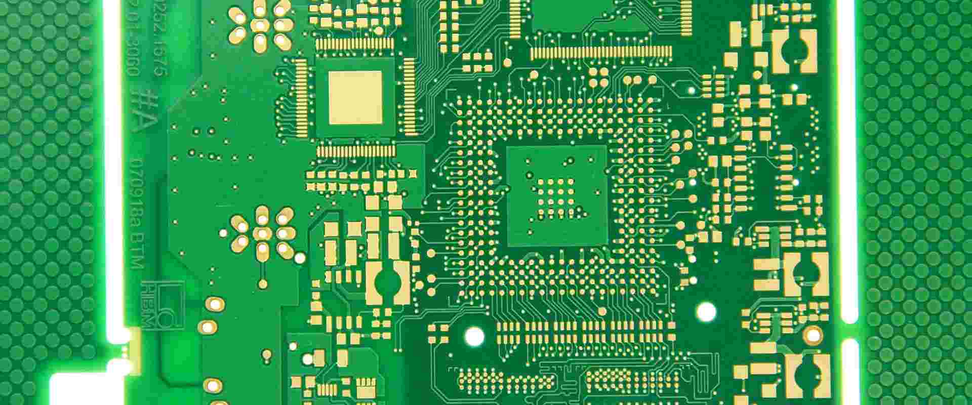
PCBs or Printed Circuit Boards are typically used to mechanically support and connect electronic components electrically using conductive pathways. Track traces, etched from sheets of copper-coated onto surfactants that are non-conductive, are used to manufacture PCBs. The PCBs are implemented in computers, communication devices, and other devices that use electricity to function.
Now that we have that covered, let us look at the Taconic TRF-43 PCB and why it stands out compared to other PCBs.
Taconic TRF-43 PCB
Taconic TRF-43 PCBs represent new generation thermally stable, low-loss overlays. These PCBs are reinforced using woven glass, which enhances their dimensional stability. Taconic TRF-43 PCBs exhibit consistent and low z-axis expansion across a huge temp range; it goes up to soldering conditions.
The TRF-43 is part of Taconic’s ORCER (Organic Ceramic) line of products. The PCBs have a DK or Dielectric Constant of 4.3 +/- 0.15 and a Dissipation factor of 0.0035. Its Thermal conductivity stands at 0.43 W/m-k.
Composition on ingredients
Taconic TRF-43 PCBs are made up of the following ingredients:
Polytetrafluoroethylene (PTFE) – 10% – 70% of the total weight
Taconic TRF-43 PCBs have a high Polytetrafluoroethylene concentration. Therefore knowing how to handle this component properly could boost the amount of time you get to use your PCB.
Polytetrafluoroethylene is a thermoplastic component that is pretty stable chemically and electrically compared to other thermosetting resins for example:
A portion of what gives Polytetrafluoroethylene the outstanding performance over temperature and Frequency also weakens the pure resin used. Due to this reason, we reinforce all Taconic TRF-43 PCBs with glass fabric. Even though the woven glass reinforcement increases the PCBS dimensional stability, you still have to take precautions while handling this product.
Precautions to take while handling PTFE
Avoid Mechanical Scrubbing
Mechanically scrubbing PTFE will deform and stretch the product. In addition, the pinch rollers we use to hold the panels while being scrubbed, leaves dents on the panel while the brushed stuff gets pressed onto the panel. Instead of mechanical scrubbing, we recommend you use chemical cleaning instead. Eliminating Mechanical scrubbing plus other unnecessary handling behaviors ultimately boosts the PCB’s subsequent processing dimensional accuracy.
Avoid picking up PTFE Panels Horizontally using a single edge
When you lift PTFE panels horizontally, you force the panel to easily flop over, which ultimately stretches the surfactant and copper. Instead, lift these panels using two edges, preferably the edges closest dimensionally close to each other.
Do not Deposit Contaminants on the Copper or substratum
To ensure that you do not contaminate the copper or surfactants used, you should:
Use slip sheets
Wear protective gloves while handling Taconic TRF-43 PCB panels
The most common contaminants include:
Fingerprints
Grease
Oil
If you take proper precautions and avoid contaminating your panels, you will not have a hard time getting them off.
Avoid Mechanical Rubbing of the PTFE Surface right after removing/etching the Copper
If the PTFE surface is left untouched, it is pretty good for bonding, prepreg, and adhesion of solder masks. However, the PTFE etched surface is prone to wetness because of the tooth structures left behind after etching. In case the surface is disturbed, you can improve its adhesion and wettability via plasma etching and the use of sodium.
Avoid stacking the Panel one onto of another
Debris or particles found on one panel can leave imprints onto the surfactants and copper of the adjacent panel. Therefore, we recommend that you store the panel racked vertically. If you must stack the panels, then implement a soft, clean slip sheet in between each panel. Also, ensure you keep the stack’s height to the absolute minimum.
Drilling holes in PCBs is a great factor to consider. Messing up while drilling could mess up the entire PCB, so here are some guidelines to follow.
You should always use the recommended Taconic drill parameters to attain the best hole quality. PCB carbide drills, standard 130 degrees point geometry, are great for drilling Taconic PCBs that are PTFE based. However, the drill’s sharpness can significantly affect the hole’s quality. Therefore, consider implementing new drills to attain incredible hole quality. In addition, it is advisable to implement a pressure limit of 40 psi; this should only increase if the topside burring becomes excessive.
The drill’s parameters determine how many hits a drill attains. These parameters are set according to the panel’s overlay thickness, stack height, and hole size. A worn-out drill bit will eventually result in many nodules that one may notice even after plating. Regular drill hit count ranges between 1500 and 500 hits for Taconic TRF-43 PCBs.
After drilling, you should get rid of all the debris occurring during the process. You can implement high-pressure water blasts to remove debris from the hole. If you implement water pressure to remove debris, ensure you bake the PCBs overlay for about an hour at 1210C to get rid of moisture before hole treatment.
What about unsuccessful drilling?
If you do not meet the drilling conditions, then burring might occur. If this happens, we recommend that you avoid sanding. Instead, implement pumice scrubbing, although processes that harm the PCBs overlay are greatly discouraged. But, again, the best solution is to fully understand the drilling conditions and parameters.
If smearing occurs (a condition whereby the PTFE resin gets heated and softens), you should:
Reduce the drilling speed (assuming that you are implementing a sharp bit) this reduce heat build-up
Gouging or hole wall tear-out is another condition that might occur during a drilling process. Gouging mainly occurs due to using an excessively high chip load or a dull drill. However, even the fiberglass weaved style might also cause gouging. A coarse glass is more likely to have gouging compared to a fine or medium glass style. If you identify gouging, you should check on the drill bit first before moving on to change the drill’s parameters. If this does not get rid of the gouging, try changing the drill’s chip load, this should do the trick. Ensure you keep the drill bit’s temperature to an absolute minimum by keeping low surface feet per minute while adjusting the drill’s chip load.
Now that we have all the handling information required to work with a Taconic TRF-43 PCB, let us look at its reactivity and stability.
Conditions that you should avoid entirely – avoid overheating the PCBs. High temperatures led to the production of toxic or irritating fumes.
Incompatible products – powdered metals, finely divided aluminum, acid, acetylene, and strong oxidizer, for example, fluorine.
Products that cause hazardous decomposition – include hydrogen fluoride, carbonyl fluoride, and Fluorinated hydrocarbons.
Disposal Considerations
Disposal should occur following the local, state, and federal regulations. You should dispose dry solids in landfills that are registered, licensed, or permitted to handle the solid industrial waste. Incinerate only when you are sure that the incinerator can scrub out hydrogen fluoride plus other acidic products released during combustion.
Conclusion
PCBs have flooded the market, making it hard to choose the right PCB to implement. However, we hope that this article has brought to light the uniqueness of the Taconic TRF-43 PCBs and why they stand out compared to other PCBs. Its efficiency and effectiveness is unmatched globally. Hence the next time you hit the market to buy a PCB, ask for the Taconic TRF-43 PCBs if you wish to buy a quality product for your project.
Do you own a computer? Do you feel a sense of uncertainty about whether it is worth investing in the new technology? All these uncertainties can be solved when you know that QuickLogic pASIC 3 Family is the best computer available in the market. This blog will discuss some of its features and how they can benefit your workflow.
QuickLogic pASIC 3 Family is a fantastic computer built on innovative technology that makes your work easy. It comes with a 4th gen Intel Broadwell i7 Processor, turbo up to 3.1GHz, 8GB DDR3L RAM, and 256GB SSD storage. In addition, its software is entirely new and can be read easily according to the user’s needs.
The very first thing we notice about this computer is its performance. Its speed is really fast. Even though it has 8GB RAM, it can process many things at once. In addition, you won’t have a problem moving around your applications because of its 256GB SSD storage. The system will load applications faster than you think, and with just a single click on your mouse, you will be able to use them easily.
FPGA was a new concept in the field of computers. It is a software-configurable silicon device that can perform various functions. Moreover, it is flexible enough for one circuit to perform many different tasks as needed.
It wasn’t as strong as what we have today in its early days, but with improvements in technology, we were able to advance in the field and make more functional solutions that help us work better. One example is QuickLogic pASIC 3 Family, which has taken the FPGA technology to another level using Field Programmable Gate Arrays (FPGAs). These devices are used to speed up computation and can become high-performing processors.
The same technology is helpful in other systems, such as the Xilinx Zynq-7000 All Programmable SoC (AP SoC), which has an FPGA and a processor core on the same device. We can program the FPGA at will without soldering new logic gates or rewiring any interconnects. This feature makes it a lot more efficient than its predecessors.
High demand for FPGAs in new applications
FPGAs are helpful in diverse applications, including communications like routers, military uses, and gaming consoles. They are also beneficial in different fields such as signal processing, computer vision, and embedded control system applications.
In the field of data centers, they help control the power and cooling of servers. However, many other applications use FPGAs. For example, these devices are helpful in servers, multimedia, telecommunications, and industrial control systems.
FPGAs have brought new demands for their performance, RayMing PCB and Assembly is investing their research and development. The technology is now readily available for everyone to afford with new hardware or a monthly subscription plan from Data Plane Development Incorporated (DPDI).
How does it work?
It acts as an instrument with an oscillating frequency that you can control using software or hardware. This will do to send frequency signals to the FPGA’s pins, and it will control which signal gets in. These FPGA pins can connect to different parts of our system by using software, or you could use a computing device.
The first thing you need to know about the QuickLogic pASIC 3 Family is how to use it. You may want to get into the process of designing your computer, but there are many benefits in getting someone to design one for you. The hardware and software are updated regularly to work with many different applications.
We will be providing you with a step-by-step process on how you can design your computer. So if you don’t want to take the time to do this, we can help you design it for a low monthly fee. It is one of the best ways to save your money upfront, and in the long run, it will save you a lot of hassle. We will explain all these things in more detail when we get into the next section.
A custom-designed computer should come with all the specifications needed to complete its tasks efficiently. You need to choose between the different performance levels it can afford to offer. It also often comes with a touch screen, making it easier for you to use.
This Family is one of his many inventions and the first to get introduced to the public. He created this computer on FPGA technology and new architecture that makes it scalable and resilient.
The first version of QuickLogic pASIC 3 came out in 2014 with some great features such as high-speed performance, easy access to new features, and easy upgrades to future applications. This led to it being one of the fastest computers of its kind.
In September 2016, a new version of QuickLogic pASIC 3 was released, which could utilize FPGAs in hardware. This made it one of the best choices for those who want a lot of versatility and better performance.
In March 2018, we saw a new QuickLogic pASIC 3 with some very strong improvements. It improved all its hardware and software capabilities and was even able to go beyond expectations by making it ten times faster than what it used to be before.
How does it work?
The main components installed on this system are CPU, GPU, RAM, and hard drives. These are all needed to complete the tasks required from your computer in everyday use.
We have seen that QuickLogic pASIC 3 is an ideal solution for many purposes, but networking, web development, and computer security appliances are the most popular ones. In addition, it’s a very powerful system that can help create new platforms and hardware.
The hardware of this system is also flexible enough to be used in different applications. Therefore, you do not need to worry about compatibility issues. It can serve many purposes, and it can even be helpful in several ways to increase its overall performance.
Some people use it as they would with any computer, while others leverage its security capabilities. The system can also be helpful to increase the overall performance of any computer.
The high-performance device will give you access to much processing power and speed. You can now expect that your system will run applications at the same speed that you do.
The performance of this system will also depend on how many cores are present in it. QuickLogic pASIC 3 can support the number of cores is approximately 32, with a maximum speed of 300 MHz and a latency of 1.25ns.
The clock rate is always affected by the number of cores in your system, but this device can go as high as 300 MHz, which makes it one of the best devices of its kind.
400 MHz Data path speeds:
The QuickLogic pASIC 3 Data Path is responsible for handling all the data to be processed, so this feature is of utmost importance.
Under six ns input + logic cell + output total delays:
The response time for these operations is quick, and it only takes about six nanoseconds. You will be able to run the most intensive applications and a lot of available processing power.
6 global clock/control networks:
The QuickLogic pASIC 3 has a maximum of six global clock/control networks. This will help the system run very efficiently because the number of tasks you can handle can increase instantly.
Two array clock/control networks:
The QuickLogic pASIC 3 has two array clock/control networks, which means it can keep running very efficiently. It will be able to manage the data from the back end.
8 high-drive input/distributed network pins:
The QuickLogic pASIC 3 has up to eight high-drive input/distributed network pins. This will help the system run parallel tasks very efficiently, and you can expect that the system will be able to keep running at a high rate of speed.
308 bidirectional I/O pins:
The input/output pins are up to 308. This will help the system have a lot of operations running simultaneously without slowing down much.
I/O cells:
You will be able to control the input and output of each pin individually. This is an excellent feature to have when handling applications that require a lot of processing power. In addition, it can help the system to run parallel tasks very effectively.
PCI compliant:
The PCI buses will give you a lot of flexibility, and you will be able to use the device at any level of speed. This is an excellent feature because you can use it in all applications.
Interfaces:
The QuickLogic pASIC 3 interfaces with both 5.0 V and 3.3 V devices. You can now expect that the system will support several great applications.
Comprehensive design tools:
The design tools can be as user-friendly as possible, so using them should not be too much hassle.
Variable-grain logic cells:
On the QuickLogic pASIC 3, you will be able to use variable grain logic cells. This means that we have a lot of choices when it comes to performance and speed. However, you can switch them based on your requirements, and this feature is also beneficial when creating networks or distributing them.
Complete pin-out stability and 100% routable:
The QuickLogic pASIC 3 is a very user-friendly device. You will be able to use it to create applications you need without having any problems.
0.35 µm four-layer metal non-volatile CMOS:
This is an excellent feature because you will be able to use the QuickLogic pASIC 3 even in small and compact devices.
Sixty thousand usable PLD gates:
You will also have up to 60,000 usable PLD gates. This will give you a lot of processing power, which is something that all kinds of users will appreciate. You can now create your applications without having any problems.
Power Consumption: active: < 60 mW; standby: < 40 mW
To calculate delay, the clock system is assumed to be running at 50% of the data rate. So, if data is generated every 20 ns, this is the time it takes to generate a single word: 25 ns. So then k=0.5/20 ns=1.6 nS
The following table gives the minimum and maximum delay time for each logic direction for each type of pin and address:
Min delay is the minimum time required for a rising edge to propagate from pin to output for a given address. It takes the same time for a falling edge to propagate from the output back to the pin. The maximum delay represents the worst-case propagation time from the output pin to the input pin.
Max delay (min delay) is 393 ns (300 MHz) * 25 ns/word * 1 word = 9 ms. Thus, multiple words (a frame) will complete in 9 ms if there are two physical clock phases, which reduces further as each phase has half the data rate of an individual phase. This means that k is [0.5/N] where N=2. Thus, the maximum max delay would be k/N rather than k.
JTAG
The maximum JTAG speed depends on the output clock’s data rate and the number of word transfers that we can do in 125 ns. Thus, to calculate max JTAG I/O speed, we know that 125ns equals [0.5/N] where N=4. The minimum k for a good value for N is [1/k]. An 8-bit I/O cell can achieve this maximum speed if we meet the following conditions:
τ = 125 ns (under normal operation)
Note: To meet this condition, all four input pins need to accept the same word at a time.
ASICs and Microprocessors pose many design challenges. However, they are very similar in a way since they both contain “Logic Gates.” Therefore, the process that needs following in ASIC design is similar to designing an IC. Therefore, many consideration needs consideration when creating these logic designs.
Step 1: Preliminary Design Work for ASIC Designs
Designers begin with a low level of abstraction and create the schematic, layout, part, and package descriptions for pre-layout tasks. After finishing this, the designer can then move on to the next step by creating a logical view of control signals and interconnections. This is called block transfer design.
Step 2: Logical View Creation
We create the logical view after finishing the block level design. The main components of this stage include the following:
Designers have a general idea of how the circuits are connected and what signals are present. This is most likely not at a level that can be simulated but has enough information to generate masks for photomasks
This will cover all the design components such as I/O pins, memory blocks, clock distribution network, etc. It will also include any extra circuitry or modules needed for special purposes or features
Simulators analyze the design and check for timing errors, functionality, or any potential errors
The next step is to make necessary changes to the circuit to correct any errors found
Once all errors are corrected, the layout can begin.
Step 3: Physical Layout Creation
Physical layout creation is a process of building up the physical layers of a chip using cells for each block and macrocells for each large functional block in the circuit design, such as memory blocks and bus controllers. Each cell consists of hard macros of gates that represent subcircuits or blocks in their entirety and soft macros which represent small portions of circuits like logic gates or registers.
Step 4: Layout for Placement Creation
After laying out the design, it is time to consider where we place each pin of the IC. A process known as placement creates a uniform layout across the chip. This means that ICs with different functionality will result in different layouts due to available resources. However, they are still in the same way on the chip.
Step 5: Floorplanning and Routing
After placement is complete, floorplanning begins. This involves arranging I/O pins to meet specific pin budgets or other design specifications, such as the maximum distance between pins. This is also the time to consider how routing resources will be helpful. This involves two main steps. First, all cells with an I/O port need to be assigned a specific routing net group. Second, create a list of connections between these ports and other pins in the layout (which may require intermediate routing stages).
Step 6: Design Rule Checking and Finalization
This step determines whether the design meets the design rule specifications. It also ensures that everything is finished and completed so that masks can be created for each photomask layer and sent off for creation. During this step, we gather timing reports to see if we meet the timing requirements.
Step 7: Mask Creation
Create the necessary mask layers for each photomask. Usually, this includes a top layer, a second layer for metal interconnect and the third layer for diffusion etch. Etching helps create diffusion regions used in the doping process of transistors in ICs. We often call these ‘photoresist’ masks since they require light exposure to create the mask.
Step 8: Wafer Process and IC Testing
After ICs have been made and packaged, they must pass multiple tests. This ensures that they are functional and correct. Again, an outside company or agency does this step.
Step 9: Final Engineering and Tape-Out
The final step in the process of IC design is the creation of a completed IC design file to manufacture more physical chips. This includes ordering masks, creating a netlist, and other necessary files to create more ICs. This is also known as tape-out since ICs become ‘tape’ that we can send to factories.
A major issue with an ASIC is a large amount of time used for fabrication. It may take about four months for a new ASIC to complete due to how long it can take the machines to fabricate an IC. The cost of creating an ASIC is about $500,000 for each chip that arises due to charges for photomasks and wafers. This does not include labor or other research costs associated with designing an IC.
The main advantage of using an ASIC is that it tends to have lower power consumption than a microprocessor. This is because the chip is simpler, which means less energy is helpful. This reduces the costs of making the ICs, thus lowering costs for both hardware and software companies. This can lead to more profitable and cost-effective products for customers.
Although it may take longer for an ASIC design to complete, new chips can be created faster than microprocessors can be updated, thus making them more effective and more usable by hardware manufacturers.
HASIC (Highly Analog System on a Chip) is an ASIC that includes multiple analog components, such as resistors and capacitors, and digital components.
We can also refer to ASICs as Flash-based Microprocessors because they use flash memory. The difference between this type of microprocessor and a normal one is that it is similar to an EEPROM in that we must erase it before re-writing data. This flash memory runs at either 1.8 V or 3.3 V and has an operating frequency of 50 MHz or 100 MHz.
A Schottky diode is necessary when designing ASICs that use flash memory because they are much easier to fabricate than avalanche diodes. Avalanche diodes take ten times longer to manufacture, require more voltage and consume more power.
QuickLogic pASIC3 Family Limitations
ASICs have their own set of limitations. For example, they may not be as flexible as a regular microprocessor and are more expensive to make. ASICs that use flash memory also have problems such as being slower and having smaller storage capacity than others.
As ASICs become more complex, it is becoming harder to review data from all of the different connections on the chip at once while they are still in the process of being designed. This means that designers must reduce the complexity of their design when creating an ASIC. It will be harder to find errors inside the chip if too much goes on in it at once.
There are many ways to design an ASIC. Even though the process is expensive and time-consuming, it is still a quicker and more affordable way to create new chips than using a microprocessor. Designing an ASIC correctly can save a lot of money and become much more efficient than a microprocessor could ever be.
The QuickLogic pASIC 3 is a powerful microcomputer that can be helpful for many different purposes. The main components installed on this device are CPU, GPU, RAM, and hard drives. These are all needed to complete the tasks required from your computer in everyday use.
We have seen that QuickLogic pASIC 3 is an ideal solution for many purposes, but networking, web development, and computer security appliances are the most popular ones. In addition, it’s a very powerful system that can be helpful to create new platforms and hardware.
The QuickLogic pASIC three can be helpful in many different applications, and it is very easy to setup. Even the most technologically untrained people will have no problem operating this device, making it a very versatile solution and a very popular one.
The QuickLogic pASIC 3 is a system you can use as an Internet firewall or a media server. It can help create other types of solutions and systems, but the most important thing is that you will use it in many ways to create something new.
It’s an ideal solution for many different people, and the examples that we have mentioned here are just some of the most popular ones.
SMT, which means surface mount technology, is a very critical aspect during the manufacturing of printed circuit boards. The SMT process engineer functions as the PCB Company’s heart.
In this article, you will learn everything that you may wish to know regarding being a SMT process engineer. Also, we’ll be exploring the experience and degree you will need. Also, there is an aspect of this article that discusses the significance of the SMT process engineer during the process of manufacturing
Furthermore, we will discuss their responsibility, as well as how to become an expert SMT process engineer. Please continue reading this article to widen your knowledge in this regard.
What is SMT?
SMT, which is also referred to as surface mount technology, is a very significant aspect of electronic assembly.
This technology assists in the mounting of the top of PCBs (printed circuit boards). The assembly process of printed circuit boards makes use of this technology. Furthermore, the technology offers a very good and effective way of reducing the costs of manufacturing. Also, it assists users in using the PCB space very effectively. In addition, with the introduction of SMT, it has now become possible to produce or manufacture electronic circuits that are complex into much smaller assemblies. Now, this is when and where you will need the professional services of a SMT process engineer.
You will require the services of a process engineer when issues that are confusing happen during the assembly process of printed circuit boards. They are also needed when there is a decline regarding manufacturing efficiency and quality of PCBA products. The main duty of SMT process engineers are:
Defines the process of SMT assembly and upgrades it
Handles any abnormalities during the process
Improves the rate of decrease rejection and the pass rate
Implements and testifies special processes for manufacturing
Sets the parameters for the process.
Evaluates new processes and new components.
As the electronic technology continues to upgrade and increased demands follow electronic products, then the main responsibility of the SMT Process Engineers will not change. Moreover, there is a new requirement that has already been set to the SMT Process Engineers to be able to meet the higher increases in demand.
First, the process engineer must have the ability to predict and define the results the process changes brings to the significant implementation of the function. Once changes occur during the SMT process, the process engineer has to be very sensitive to predict the corresponding results that will result.
Second, the PE must be well aware of the tools applied during all the phases of the life cycle of the product. The leading technology is the main competitiveness by the electronic companies, which simultaneously leads to a higher requirement during electronic manufacturing.
Take for instance, some new mounter types have many modules via which process engineers easily know the SMT process. Therefore, the SMT process engineers have to embrace all the development changes any minute. This will help them perform much better in their new workshops.
What is the Importance of the SMT Process Engineer?
For the manufacturing process of SMT assembly, there are lots of elements at play, such as component package, equipment, materials, technical requirements, etc. Therefore, there has to be someone that can comprehend, explain, as well as monitor the entire process.
Furthermore, the strong competition found between workshops and companies globally causes them to improve the technologies for manufacturing actively in the electronics field.
There’s more. The progress regarding technology brings more possibilities. i.e. You must handle more complicated and smaller components and environmentally-friendly technologies like soldering (lead-free) more carefully.
Furthermore, the entire trends give the SMT PE both challenges and opportunities. Concerning their opportunities, this tells that all electronic workshops need to be dependent on the SMT process engineers. This will help in optimizing the process involved in their manufacturing process.
As regards their challenges, the process engineers stand at the main focus of profit increasing so far it involves electronics companies.
The new era is seeing higher demands placed on the process engineers of printed circuit boards so that top SMT process engineers ought to perform well both in modern technologies, as well as traditional tasks. Also, the significance of the industry depends on their role.
Top SMT process engineers have to know much about the processes involved in SMT manufacturing and supply chain. Also, they should be able to treat the two as a whole thing.
To be very competent in every responsibility and task, process engineers must win much higher demands. Also, they shouldn’t just be enthusiastic in every improvement, rather they should work harder for very clear directions.
Asides from this, they have to be cooperative. This is because there’s a need to constantly check the quality of manufacturing and draw up a manufacturing plan. In order to achieve these, process engineers must have high analysis, as well as vast knowledge regarding Statistics Process Control (SPC).
It takes so much time for a process engineer to record as well as collect data. However, you can perform the task easily by using the newest tools and machines. These tools and machines have the ability to increase efficiency and improve programming.
Also, they play a vital role in assisting the process engineers in analyzing large quantities of data. Furthermore, they monitor the important technical parameters automatically.
This is why process engineers have to learn how to utilize these machines that help in inspection. Immediately there’s a change in technology, the whole tool can influence the entire technology in just a few seconds.
Therefore, the process engineers must learn to work and depend on scenic technology and data models to imitate new technologies. By doing so, there will be no use for tests to be carried out over and over again.
Conclusion
We hope we have been able to explain and answer the question “what is a smt process engineer in manufacturing.” They play a major role in PCB manufacturing. If you need more clarity, please ask your questions.
The .NCD file is a Nero Cover Designer application. Files that feature .ncd file extension are associated with the .NCD CD/DVD label design software.
NCD files feature the layout, graphics, and text included in the design of the cover label. There are several software applications that utilize the .ncd file suffix. An example of such software is the Norton anti-virus software.
The .NCD file is a Cover Designer created by Nero. This file extension is commonly associated with files featuring CD or DVD labels. Also, these files feature artwork designed with CoverDesigner. The CoverDesigner is a software for making DVD/album cover designs. Also, it is part of the Nero multimedia suite. Its NCD files consist of text, layout, and image settings that comprise the cover art design of a CD.
Also, the NCDC is a file extension the CD maker uses as the default disk image format. These NCD files have an exact copy of information gotten from a compact disc. The new version of CD Maker, Media Maker Express supports NCD disk image format. ISE Design Suite saves native circuit descriptions in NCD files.
One of the most common ways of opening a file extension NCD is by double clicking it. However, this might not work at times. If this doesn’t work, there are a few ways to open the .NRD file.
Select the right program
It is important you choose the right program. There are some programs that allow you to open the NCD files easily. These programs include:
The type of file you are opening is very important. Some programs can open your NCD file. However, this depends on your file type. To know the type of file, check the properties of the file. Right click the file and check properties and view the “Type of File.” If you are using a Mac computer, right click the file and select “More Info” and check under “Kind.”
Make use of a Universal File Viewer
This is the easiest way to open a .NCD file. For instance, File Magic can open several file types based on the format. Some files may not work with these programs. The NCD file will appear in a binary format if it isn’t compatible.
Ask the Developer
One of the easiest ways of opening an NCD file is to contact the software developer.
There are several programs that can help you open and convert your NCD files. These programs include:
ISE Design Suite
This is an integrated development platform for designing CPLD and FPGA devices of Xilinx. The NCD file stores ISE design suite’s native description data.
Media Maker Express
Media Maker Express created by NTI is a media backup and disc burning software application. This program features several burning engines and improved disc image support. Media Maker Express can read and write disk images in NCD format. Also, this file format is a Disk Image.
Dragon Burn
Dragon Burn by NTI is a MacOS application designed for burning media content to DVDs and CDs. Also, you can use it to clone and make disk images in different formats including NCD.
Norton 360
Norton 360 by NortonLifeLock is a comprehensive anti-spyware and anti-malware program for mobile and desktop devices. The .NCD files saved some change directory data utilized by Norton 360’s older versions. The more recent version seems not to use this file.
IsoBuster
IsoBuster by Smart Projects is a disc burning application that features data repair/recovery support. Also, any disk images saved in the NCD format work well with this program.
There are various reasons why you won’t be able to open your files with the NCD extension. You can solve these problems without any in-depth IT skill. Follow these steps to open a file with NCD extension.
Install Nero Multimedia Suite
The most common reason why users can’t open their NCD files is that their system doesn’t have any program that can handle NCD files. In this case, you need to download the Nero Multimedia Suite and install it. You can visit the Nero AG and download the software with the links provided. This is the safest way to download the Nero Multimedia Suite.
Update Nero Multimedia Suite if Necessary
If you can’t access NCD files after installing the Nero Multimedia Suite software, ensure it is up to date. Software developers may introduce newer versions of this application. Nero Multimedia Suite may not handle NCD files because it is outdated. The most recent Nero Multimedia Suite must support all formats that worked with its older version.
Set the default application to manage NCD files
Sometimes the Nero Multimedia Suite installed on your system might be up to date and the problem will still persist. In this case, choose the Nero Multimedia Suite as the default program to manage NCD on your device.
Ensure the NCD is not faulty
After trying the above-mentioned options you might still encounter some problems. Then, you need to verify if the file is an .NCD file. There are various reasons why you might not be able to open the file. Therefore, you need to do this:
Verify if the file is already damaged or corrupted.
Check if your PC can handle Nero Multimedia Suite
Also, check if the NCD doesn’t have a computer virus
Make sure the latest drivers and system updates are installed in your system
Conclusion
.NCD files are ideal for storing artwork documents for DVD or CD booklet inserts. If you are having problems with how to safely open the NCD file, this article is for you. We have discussed ways to open the .NCD files in this article. Also, there is well-detailed information on programs that can open and convert the .NCD files.