
RAYPCB · Shengyi materials and manufacturing
Shengyi S1190 PCB: review the dielectric between dense plated holes
Plan S1190 and S1190B construction for dense multilayers or inner heavy copper, compare hole-web geometry and organize qualification evidence.
Share your current requirements and open questions. Tool use is optional.
What is Shengyi S1190 PCB material?
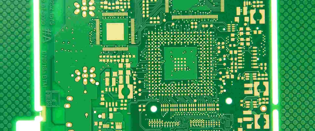
Shengyi S1190 is a high-performance rigid FR-4 laminate paired with S1190B prepreg. Its supplier identifies demanding multilayers and inner-heavy-copper constructions among the intended applications. For a fabricated PCB, that material positioning must be translated into a specific stackup, resin-fill plan, hole geometry and qualification scope. It is not a universal approval for every dense or high-layer-count board.
This page focuses on the dielectric between drilled holes and the construction around inner heavy copper. These details connect material selection to practical manufacturing questions. The worksheet calculates a geometric web using maximum drill diameters and a combined position allowance, while the surrounding guidance explains why geometry alone cannot establish CAF resistance or long-term insulation reliability.
S1190 Tg200 needs a test-method qualifier
| Characteristic | Selected typical supplier value | Why the distinction matters |
|---|---|---|
| Tg | 170°C TMA; 200°C DMA | The DMA result is not a DSC200 requirement |
| Td | 350°C, TGA at 5% mass loss | Separate from a service or process limit |
| Total Z expansion | 2.3% over 50–260°C | Interval-specific dimensional data |
| T288 | 45 minutes, TMA | A material laboratory test |
| Bonding system | S1190B | Core and prepreg identities belong in the stackup |
The reference is Shengyi's S1190/S1190B data sheet, CN-TDS-2308-04. Typical material results are not guaranteed production-board values. If a drawing says only “Tg200,” resolve the intended method and acceptance basis before approving the material rather than assigning the largest available number to the requirement.
The Tg200 PCB guide covers that broader terminology. The Shengyi family overview offers a method-aware comparison across grades. S1190's page concentrates on the construction and evidence needed when dense holes or substantial inner copper drive the engineering discussion.
Define the dielectric web between drilled holes
The simple geometric web between two circular drilled holes is the center spacing minus half the sum of their diameters. Use maximum drilled diameters for this calculation. Finished plated-hole diameters are smaller and would overstate the remaining dielectric if used as substitutes for the drilled geometry.
Position variation can reduce the actual center spacing. The worksheet therefore subtracts a combined allowance for the pair. If the two holes each have an independent positional tolerance, determine the relevant worst-case combined reduction before entering it. Do not enter a per-hole number only once and assume that both holes have been accounted for.
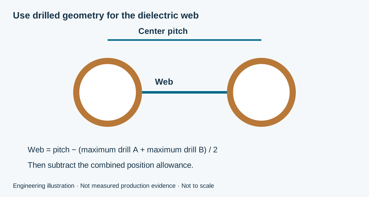
This geometric ligament is not the same as creepage, clearance, an anti-pad dimension or a certified insulation barrier. Other nearby conductors and planes can introduce different constraints. Review the complete layer map and drill structure, especially where a dense connector or component escape concentrates many holes in a small area.
Calculate a hole-web planning margin
Enter the nominal center spacing, maximum drill diameter for each hole, combined position allowance and a required geometric web taken from your reviewed drawing. Add the requirement and tolerance source so the result can be traced. The tool reports the web before and after the allowance and the difference from your required value.
RAYPCB ENGINEERING
Shengyi Material EngineeringShengyi S1190 PCB Engineering Planner
Loading Shengyi S1190 PCB Engineering Planner…
For an illustrative 0.80 mm pitch with two maximum 0.25 mm drills, the initial web is 0.55 mm. Subtracting a 0.075 mm combined position allowance gives 0.475 mm. Against an entered 0.50 mm requirement, the difference is −0.025 mm. This identifies a geometric shortfall against the supplied requirement; it does not predict whether an actual board will develop CAF.
The worksheet rejects a worst-case geometry in which the holes touch or overlap. A positive remaining web is still not a manufacturing-capability claim. Confirm drilling, registration, material construction and acceptance requirements with the fabricator. If the tool result changes after a layout revision, update the attached drawing and its requirement reference together.
Inner heavy copper changes the resin-fill problem
Thick patterned copper creates topography that the bonding material must accommodate. The required resin volume and resulting dielectric construction depend on the actual pattern, not merely on the nominal copper weight. Dense power regions, cleared areas and local asymmetry should therefore be visible in the stackup and manufacturing review.
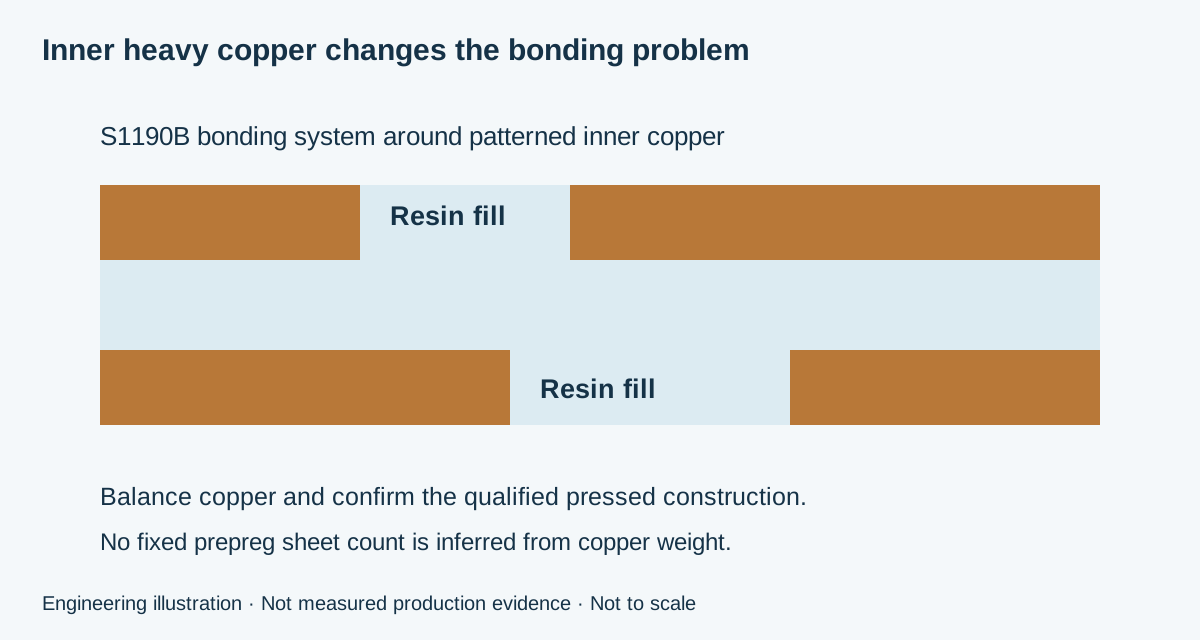
Specify the S1190 core and S1190B bonding system, intended finished copper and dielectric gaps. Ask for a reviewed pressed construction rather than prescribing a fixed number of prepreg sheets from a generic copper-weight table. Check whether the proposed arrangement preserves the mechanical thickness, reference-plane geometry and local insulation requirements that the circuit depends on.
The heavy copper PCB guide covers the wider current, copper and manufacturing task. This S1190 page does not repeat that entire topic or imply that resin selection alone solves a current-carrying problem. Electrical loss, temperature rise, transitions and cooling still require their own analysis.
What an anti-CAF discussion should actually include
CAF susceptibility concerns a material, design and manufacturing system under defined conditions. A supplier's anti-CAF positioning can inform a shortlist, but it does not establish the performance of every board geometry made with that material. The qualification plan must identify the relevant construction and the test conditions that answer the project concern.
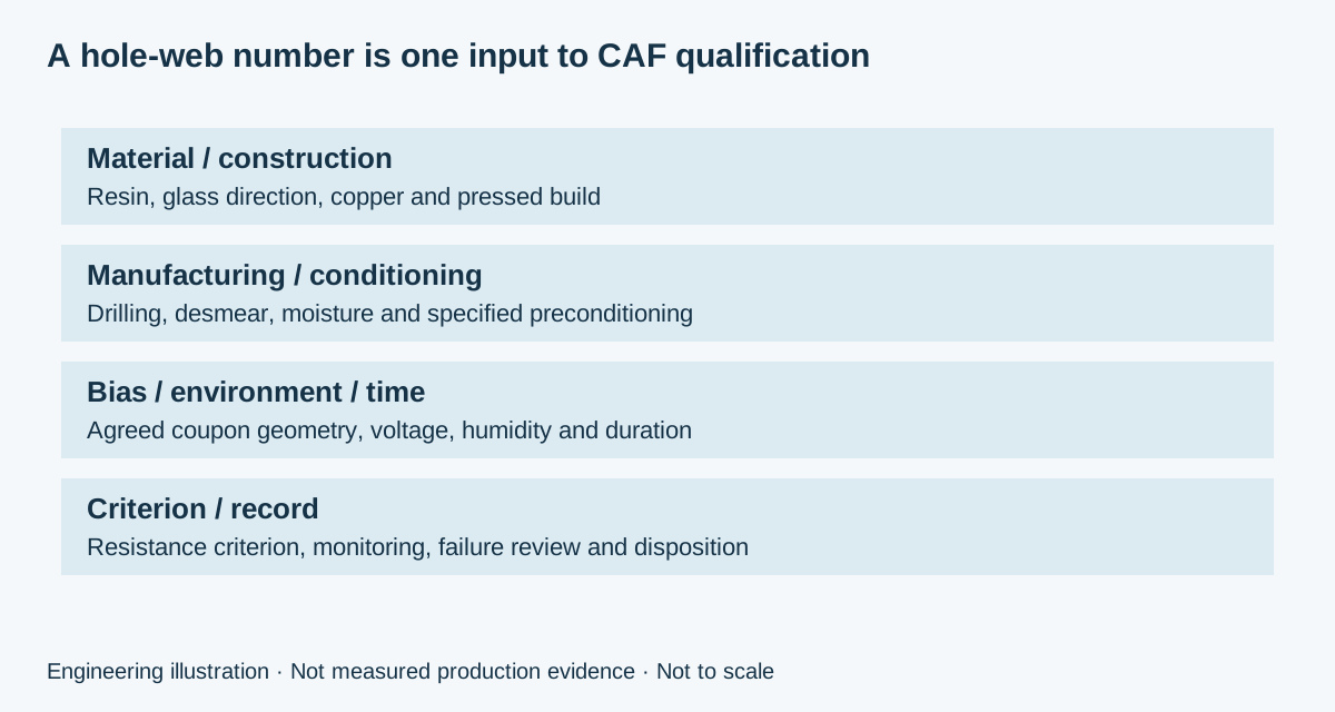
The official IPC-TM-650 method 2.6.25C provides a reference for CAF resistance testing. Review the method's scope and limitations with the qualification team. Do not copy one bias voltage, coupon spacing or duration out of context and present it as a universal requirement for every product.
Discuss material identity, glass orientation, hole pattern, manufacturing condition, conditioning, bias, humidity, monitoring and acceptance criteria. Agree which sample construction represents the production design and how changes will be assessed. This produces a testable specification rather than the unbounded statement “CAF-proof PCB,” which would conceal the actual conditions of the claim.
Coordinate dense geometry with electrical and mechanical needs
In a connector-rich control board, increasing a drill web may compete with routing channels and plane continuity. In a power board, adding inner copper may compete with dielectric spacing and final thickness. Resolve these trades using the same layer map so electrical, mechanical and fabrication reviews do not each approve a different implied construction.
Identify which features are fixed by the component or enclosure and which can change. A revised via placement, layer allocation or pad geometry may be more useful than trying to solve every constraint through a material substitution. Use the multilayer PCB planning page for layer allocation and keep the material-specific decisions on the released stackup.
For controlled signals, review the actual dielectric and reference geometry after a construction change. A material's typical Dk is not a complete design value for every glass/resin combination. The controlled-impedance workflow helps organize that discussion and the associated coupon requirements.
Inspect the build that was actually ordered

Before release, agree which records establish material identity, dimensional construction, plated-hole condition and electrical connectivity. A routine bare-board electrical test checks a different concern from a CAF qualification or a thermally conditioned cross-section. Keep the purpose and scope of each result clear in both the quotation and the acceptance plan.
The PCB electrical-testing page explains the netlist test route. Additional construction or reliability evidence should be specified separately, including representative samples, test method, acceptance criterion and report responsibility. A photograph of an inspection machine does not establish that the required test was performed on a particular lot.
For repeat production, retain the fabrication revision and approved construction with the qualification record. Changes in copper pattern, board thickness, drill geometry, material source or process may need reassessment. Define who authorizes that assessment so an apparently small procurement substitution does not bypass a requirement established during development.
What drives an S1190 PCB quotation?
Cost depends on the exact core/prepreg construction, layer count, copper distribution, hole geometry, quantities and evidence requested. The use of a particular laminate does not by itself define the fabrication complexity. A dense multilayer and a simpler board can have different process and acceptance requirements even when both specify S1190.
Request the same revision, quantity basis and test scope when comparing offers. Separate recurring fabrication from setup, special tooling, coupons, qualification samples and reporting. If material availability or an alternative construction is being reviewed, identify the consequences for qualification rather than comparing only the immediate unit amount.
RAYPCB ENGINEERING
Shengyi Material EngineeringShengyi S1190 PCB Budget Brief
Loading Shengyi S1190 PCB Budget Brief…
The budget brief is specific to the S1190 construction task and starts without rates. You may export only the technical requirements, or enter a complete set of dated allowances for transparent allocation. There is no automatic heavy-copper surcharge or live supplier price. Send the current hole and copper requirements with the brief through Contact for an exact review.
S1190 PCB questions
Is S1190 a DSC Tg200 material?
The linked sheet reports 200°C by DMA and 170°C by TMA. It does not justify rewriting those values as DSC200. If a purchasing specification requires a particular method, obtain evidence for that requirement or clarify the specification before material approval.
Why does the worksheet use drilled rather than finished holes?
The geometric dielectric web is bounded by the drilled holes. Copper plating reduces the finished opening, so using the smaller finished diameter would make the apparent web larger. Use the maximum relevant drilled dimensions and include the combined positional effect for the pair.
Can a larger web guarantee CAF resistance?
No. Geometry is one part of the material, construction, process and exposure system. A larger calculated ligament is not a qualification result or an operating-voltage rating. Agree the representative test construction and conditions that address the actual reliability requirement.
Does the supplier's high-layer application statement prove factory capacity?
No. A laminate's intended application and a fabricator's qualified build capability are separate subjects. Send the actual layer map, dimensions, copper and hole requirements for engineering review. The accepted manufacturing and inspection plan must describe the specific construction rather than relying on a broad material application label.
Request S1190 PCB manufacturing review
Send the named laminate and prepreg, drawing revision, stackup, quantities and required evidence. Identify open material, construction or qualification questions so engineering can prepare a useful manufacturing proposal.
Attach a downloaded tool brief manually. Contact does not automatically receive these inputs. References reviewed September 2026. Illustrations use planning examples; photographs do not establish prices, delivery times or project-specific acceptance.

