Top 15 rigid flex PCB Manufacturers in the World

rigid flex PCB Manufacturers

For a flexible PCB, you’ll need a reliable manufacturer. Here are the Top 15 Rigid-Flex PCB manufacturers in the world. Ray PCB specializes in manufacturing Printed Circuit Boards that have three-dimensional connections. This PCB manufacturer offers quality at an affordable cost, and they ensure that the PCB design is of high quality.

Zhen Ding Tech

Taiwan’s leading flexible PCB manufacturer, Zhen Ding Technology Holding Ltd, has recently secured approval for its IPO from the China Securities Regulatory Commission. In addition, its Shenzhen-based subsidiary, Avary Holding (Shenzhen) Co Ltd, was approved for its initial public offering on Aug. 24. The company is a subsidiary of Zhen Ding Tech Holding Ltd.

The firm is a supplier to Apple and has recently expanded its offerings to include COF substrates. We anticipate this growth in demand to continue as other smartphone manufacturers, including Apple, move toward SLP-based PCBs. Meanwhile, a recent study by Nidec, the Japanese motor manufacturer, showed that hard-drive shipments might fall by 50 percent this year, indicating that Zhen Ding is in the correct position for future growth.

The company’s highly skilled and experienced staff has made it one of its top 15 rigid-flex PCB manufacturers. With a history of innovation and superior PCB quality, Zhen Ding Tech has established itself as a leader in the industry. The company’s advanced ELIC and HDI PCB have paved the way for breakthrough products in communication technology. The firm also produces many high-layer-count PCBs.

RayMing Technology

This year has seen several significant developments at RayMing Technology. First, it got the U.T. Inventions of the Year Award. Second, it invested in new testing equipment in its Shenzhen factory. Third, the company acquired Marcel Electronics International and KCA Electronics. Fourth, the company expanded its facility in Malta by 1,250 square meters. Fifth, it completed a comprehensive PCBA testing process that includes in-circuit and functional tests.

RayMing Technology, also known as Rayming PCB & Assembly, has extensive experience in rigid-flex PCB. They have designed hundreds of different rigid-flex PCBs for various brands. Another impressive feature of the firm is its excellent rigid flex PCB design guidelines tools, which help them complete rigid-flex PCB projects in an accelerated time. One of the most common concerns of rigid-flex PCB is the lack of space inside the board. Rayming PCB & Assembly has several experienced engineers who can help you design your rigid-flex PCB to solve this issue.

Sun&Lynn Circuits

One of the leading PCB manufacturers globally, Sun&Lynn Circuits is a domestic company that specializes in producing PCBs with both soft and hard bonds. It spearheaded the first mass production of circuit boards in mainland China and is one of its most environmentally friendly PCB manufacturers. Its technological innovations and efforts to improve local circuit board factories have earned it among the top 15 rigid-flex PCB manufacturers worldwide.

The company has invested heavily in advanced manufacturing equipment and has a highly skilled rigid flex PCB design team. The company invests around 5% of its annual revenue into research and development. Its manufacturing facilities boast some of the world’s most advanced machinery and have distinct divisions for each stage of the production process. In addition, sun&Lynn Circuits also provide high-quality flex-rigid PCBs.

Yongfeng Group

With their uL 94 V0 and UL 164 ratings, we can evaluate the high quality and reliability of the rigid-flex PCB manufacturers. They should also have the latest and most effective software to ensure the smooth operation and nullification of printed circuit board errors. Moreover, they should have U.L. certification, the most trusted symbol of rigid flex PCB fabrication quality.

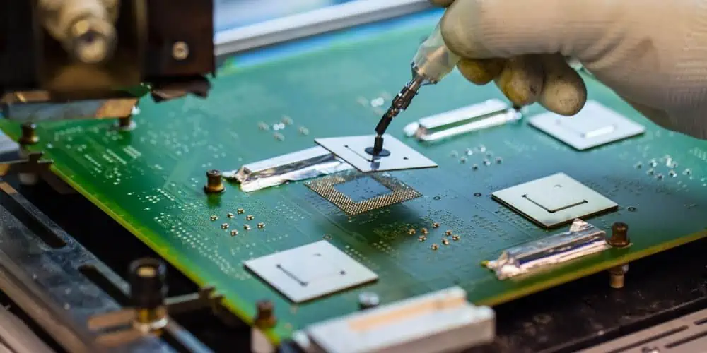
PCB Rigid-flex is a hybrid printed circuit board combining rigid-flex and flexible-flex circuits elements. It can bend and maintain its shape, and the flexible film between the two rigid PCBs can help the rigid-flex PCB maintain its structure. In addition, this type of circuit board offers improved electrical performance and added functionality.

IEC Electronics Corp.

The company is primarily known for its work with electronic contract manufacturing services, circuit cards, and loads of wire and cable. The firm has more than 1,300 people and employs the latest equipment to create electronic products.

During the first two years of operations, IEC Electronics Corp. was profitable. The company had revenues of $3.3 million in fiscal 1974 and $4.06 million the following year. But IEC’s fortunes began to turn around after entering the consumer products market. Besides T.V. games, IEC also manufactured VHF and UHF portable radio transceivers, paging receivers, and a base-station encoding control system.

Murrietta Circuits

The manufacturing process for rigid-flex PCBs is not difficult. Advanced technology and modern equipment can help manufacture the boards. Moreover, the company uses modern materials like immersion tin, chemical gold, and polyimide. The company also provides burn-in services for the boards. It is one of the top 15 rigid-flex PCB manufacturers in the world.

The best rigid-flex PCB manufacturers combine flexible and rigid circuit board technology to create a unique board design. Its inner consists of multiple flexible circuits held together by an epoxy pre-preg bonding film. This hybrid technology offers many advantages in signal transmission and assembly. Also, it is a smaller size than a standard PCB.

A.P. Circuits

With more than two decades of experience, A.P. Circuits has become one of the world’s leading manufacturers of flexible printed circuit boards. They focus on innovation and efficiency in designing, manufacturing, and assembling diverse PCBs. Their expertise extends to the medical, aerospace, and portable electronics industries. Read on to learn more about what makes A.P. Circuits one of the top 15 semi flex PCB manufacturers.

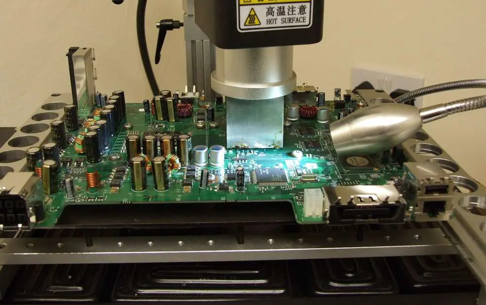
The manufacturing process of rigid-flex PCB is complex. First, we apply a liquid coating to the circuitry. This liquid coating is either acrylated epoxy or polyurethane. Screen printing is the most common process for applying liquid coatings. The liquid coating is then thermally cured. For rigid-flex PCBs, copper is the most popular material. It is an excellent electrical conductor and resists corrosion.

Shenlian Circuits

Shenlian Circuits is a national high-tech enterprise in China with more than 400 employees specializing in both flexible and rigid printed circuit boards. Their PCB production techniques are advanced, and their designs are ideal for the application. The company has advanced production tools and meets the demanding schedules of its customers. To ensure that you complete your product on time, you can trust Shenlian Circuits to design and manufacture your PCBs according to your specifications.

The company specializes in flexible and thin rigid PCBs. Its products are widely helpful in mobile phones and digital cameras. Another company is Shenlian Circuits, which specializes in high-precision FPC manufacturing. Other leading companies include Dongguan Kejia Circuit Technology Co., Ltd., which has been in the electronics industry for over 15 years and employs over 600 people.

SigmaTron International

It can be challenging to find a company that can meet your specific needs for rigid-flex PCB manufacturing. The quality of flex PCBs depends on many factors, and not every manufacturer can meet these requirements. Fortunately, there are a few things you can look for in a flex PCB manufacturer. These include: How experienced is the company? Can they offer prototype development? How much of a turnaround time do they require?

In addition to high-quality designs, Proto Express also offers multiple services to meet customers’ needs. Its multiple fabrication stations in China and a business model that emphasizes sustainability are two of the company’s selling points. Other noteworthy aspects include an emphasis on innovation, rationalization, and efficiency. In addition, it invests in advanced materials, such as HASL and OSP, for its production process.

Unimicron Technology Corporation

Unimicron Technology Corporation is a Taiwanese manufacturer of printed circuit boards. It manufactures high-density interconnection boards (HDIBs), rigid-flex PCBs, and integrated circuit carriers. They also offer burn-in and testing services for PCBs and I.C. substrates. Read on to learn more about Unimicron and its many products. This Taiwan-based company produces high-quality PCBs.

It manufactures and distributes printed circuit boards, multilayer PCB, and I.C. testing products. The company also offers various electronic assembly services, including PCB manufacturing. Its products are helpful in many electronic devices, from cellular phones to tablets to global positioning systems and memory cards. In addition to manufacturing printed circuit boards, the company also offers services and products for I.C. burn-in and testing.

Founded in 1990, Unimicron is a Taiwan-based manufacturer of printed circuit boards and electronic products. Its products include high-density interconnect boards (HDI), rigid-flex PCBs, and flexible PCBs. Additionally, it offers I.C. carrier and connector testing systems to the electronics industry. Unimicron is the fourth-largest manufacturer of flex PCBs. Unimicron produces more than 20 different PCBs and I.C. carriers each year.

DSBJ

The company provides solutions for the automotive, telecommunications, and industrial markets. Its products include semiconductors, microprocessors, flash memory, and integrated circuits for quantum computing and artificial intelligence. It is also a member of the PitchBook Platform, but you need to be a member to see its full profile. If you’re looking for a publicly traded company, you might want to invest in DSBJ.

DSBJ started operations in 1980 but has quickly grown to become one of the world’s largest precision sheet metal components suppliers. Based in Suzhou, China, DSBJ produces a range of electronics, including mobile phones, T.V.s, home appliances, and telecom equipment. It also manufactures LED packaging and display modules, focusing on LED and OLED technologies. In 2017, DSBJ generated annual revenues of around US$2.2 billion.

Tripod Technology Corporation

Taiwan-based Tripod Technology Corporation manufactures printed circuit boards and multilayer PCBs. The company’s products are helpful in personal computers, peripheral devices, communication, industrial instruments, and consumer electronics. The company operates through two segments: PCBs and Others. We can find its products in domestic and international markets, including China, Korea, and Malaysia. The company also manufactures and sells various products, including electronic components, automotive parts, and memory modules.

The company’s dividend is paid every six months and covers approximately 75% of its costs. In addition, Tripod has an outstanding track record, having been one of the fastest-growing private companies in 2008 and 2009.

Kinwong

Among the top PCB manufacturers, Kinwong has gained considerable recognition for its ability to deliver superior circuit boards. This company specializes in producing circuit boards for medical devices and consumer electronics. Many consumers of these electronic devices praise the efficiency of these circuit boards. In addition, the company can meet the needs of various customers and ensure quality assurance at every stage of the process.

There are over 3,000 manufacturers of printed circuit boards in Asia, and the number is growing faster than the global demand. However, many manufacturing shops are reducing their prices to compete, and this strategy hasn’t been particularly successful. These manufacturing shops have also expanded their product offerings, including flex PCBs. The report identifies the leading companies in the Rigid-Flex PCB manufacturing industry.

Suntak PCB

Suntak PCB is another top PCB manufacturer that focuses on technology innovation. Since its founding in 1999, the company has played an essential role in the Chinese circuit board industry. It has set up two manufacturing campuses in Yixing and Guangzhou and is committed to providing quality circuit boards for various industries. They have expanded their services across the globe, reaching more than 50 countries. They offer superior PCB products that help their customers increase their productivity.

Gultech

Gultech has over thirty customer support centers in China and other countries around the globe. Their customer service team focuses on PCB consumer problems. Their PCB solutions include all the required components, so you don’t have to spend time searching for the right components. Gultech’s one-stop solution for all your PCB requirements allows you to focus on other aspects of your project, while Gultech’s knowledgeable staff is available around the clock.

Proto Express

Proto Express focuses on rigid-flex PCB manufacturing. They are providing customers with high-quality designs at reasonable prices. Proto Express uses OSP, Immersion Gold, and HASL for surface finishing. They also offer flexible flat cable solutions, so you can be certain that your boards will be of the highest quality. These companies have been in business for more than six decades, and their products have been helpful in countless industries.

Top Four Benefits of Rigid-Flex PCB Fabrication

If you’re in the process of creating a product, you’ve likely considered the benefits of a rigid-flex PCB. This fabrication method is flexible and customizable yet sturdy enough to withstand heat and U.V. rays.

Customizability

A rigid-flex PCB can be customized to fit your device and design specifications. This allows you to design the board according to your specifications and your customers’ requirements. Because the rigid-flex PCB is a custom-made product, we can manufacture it in any shape and size. You can also get it in a different material than the traditional PCB. It’s the perfect solution for prototype and production environments.

The benefits of this flexible and rigid-flex PCB are numerous. For example, a 3D application with a flexible layer can save space and require fewer solder joints, which leads to lower assembly and test complexity. These benefits translate to increased electrical connection reliability and reduced heat absorption. Moreover, the flexible PCBs allow for more customization of the board to match the device’s specifications and meet the needs of various consumers.

As a result, rigid-flex PCB design can be a breeze. Designing with these boards is simple with the right design tools. You can use design software that features integrated 3D modeling and easy-to-use schematics. Altium Designer is one such solution because it offers a unified interface and platform. The software will allow you to create your flex PCB in a standardized way easily.

The flexibility of flexible PCBs also enables them to withstand extreme environments. This makes them highly reliable even in the most demanding environments. Flexible PCBs can withstand high pressure and rapid movement. For example, mobile devices can be folded to monitor vital signs and serve as conformal heating elements. Flexible and rigid PCBs are highly functional, so you don’t have to worry about their dependability or reliability.

Reliability

The Rigid-Flex PCB is ideal for the miniaturization of products. Its compact size and ability to bend and twist to fit in small spaces are suitable for designing sophisticated circuits. Since this type of circuit board is flexible, it is also lighter than conventional rigid-flex PCBs. In addition, rigid-Flex PCBs are easy to handle and install. They can also be tested and evaluated before installation, which reduces development time.

The design process of a Rigid-Flex PCB is like that of a rigid circuit board, but it includes a flexible component. This type of circuit board is also less likely to contain solder joints, reducing the product’s overall cost. In addition, the design process can be streamlined and simplified with the help of a specialized rigid-Flex PCB manufacturer.

A rigid-Flex PCB can withstand a wide range of temperatures, ideal for applications where reliability is paramount. Due to its high thermal stability, it is suitable for use in extreme temperatures. It also retains the benefits of both rigid and flex boards. The Rigid-Flex PCB is resistant to radiation, chemicals, and harsh oils. It also offers excellent shock and vibration resistance, suitable for industrial applications.

Rigid-Flex PCBs provide an excellent combination of rigid and flexible circuit boards. By layering flexible circuit substrates inside rigid PCB materials, they combine the advantages of both types of circuit boards. As a result, rigid-Flex PCBs offer superior electrical performance, greater component density, and increased flexibility. In addition because their design is more flexible, they’re more suited for complex, mechanically challenging applications.

Cost

The primary cost driver in rigid-flex circuit board production is the PCB material used. FR-4 substrates can help laminate rigid circuit boards. The flex core and coverlay layers consist of polyimide. Flexible boards have uniform thickness and improved electrical and thermal properties. The flex circuit board’s thickness is typically one to five mils compared to the usual FR-4 substrate. The flex-compatible laminate material costs approximately two to three times more than rigid materials.

PCB design costs are also a big factor when considering rigid-flex circuit boards. The flex-compatible material can help reduce the cost of designing and manufacturing the PCB. During the development process, designers can collaborate with the PCB fabricator to optimize the design for the flex-capable material. This allows for an efficient first-time build and accounts for expected product variations. While rigid-flex circuit boards are generally more expensive than standard PCBs, their flexibility and ability to withstand environmental variations make them an excellent cost-effective option.

Rigid-flex PCBs are typically more expensive than traditional PCBs due to the complexity of the manufacturing process. In addition, rigid-flex PCBs require more raw materials, which means a lower overall yield. However, rigid-flex circuit PCB manufacturers typically use materials not used for traditional PCB production. Because these materials are unique to rigid-flex PCB production, the cost is higher. In addition, those materials may not be available in your area.

Resistant to heat and U.V. rays

Resistant to heat and U.V. ray is a key component of a rigid-flex circuit board. The following materials offer the utmost heat and U.V. resistance: polyimide (or P.I.), polyester, and glass fiber. The materials are flexible and easy to handle while retaining their electrical properties. In addition, the adhesive used for rigid-flex boards should be heat and chemical-resistant.

Flexible flex circuit boards offer several benefits over rigid circuit boards. They are lightweight, flexible, and resistant to chemicals, radiation, and U.V. rays. We can easily test them, and they are suitable for high temperatures or high-density applications. In contrast, rigid-flex circuit boards should not replace traditional printed circuit boards. However, they are a superior option for industrial sensors and can work in harsh environments.

Despite its name, Rigid-flex PCBs consist of polyimide, a plastic material that is highly flexible and resistant to many assembly processes. In addition to being highly heat resistant, polyimide is resistant to multiple solder reflow cycles. Additionally, it is stable when temperature fluctuation occurs. As a result, rigid-flex PCBs are commonly helpful in medical devices and aerospace.

Requires different skillset

Manufacturers of rigid-flex circuit boards should be certified, as these products must follow specific regulations. While this may be difficult to accomplish, rigid-flex PCB manufacturers need qualified personnel to handle production details, including regular inspections and handling the large volume of orders. Moreover, if you’re interested in creating a prototype for your product, you should look for a manufacturer with a history of producing and supplying flex PCBs.

As mentioned above, designing circuits on flex PCBs requires different skillsets than rigid ones. In addition, you’ll find that prototyping flex PCBs is more expensive and complicated. Moreover, you’ll need different skill sets to design circuits for these boards, such as the ability to repair them when they’re damaged. For this reason, designers of rigid-flex PCBs should be careful not to place components on bending lines, which can result in vibration and other problems.

Although rigid-flex PCBs are more expensive than conventional ones, they offer superior electrical performance and mechanical support. The flexibility of flexible substrate material helps with impedance control and a wider range of packaging options. As a result, these boards are highly beneficial for consumer products and military and medical applications. They have a small size and a flexible center section, making them ideal for applications where space is an issue.

As with rigid-flex PCBs, assembly processes are a little different. You’ll be dealing with more flexible layers and metals, and your rigid-flex circuit boards will be more versatile. A flexible PCB may also require you to have a different skill set for a particular task. However, this should not be a deterrent. Regardless of your skill level, there are advantages to both rigid-flex and flexible PCBs.

Why Doosan Middle Tg DS-7402M PCB Material Offers Great Performance in PCB Fabrication

24 layer pcb

PCB manufacturing is a process that requires different raw materials. Therefore PCB laminates are one of the most crucial materials. It is essential to use quality PCB laminates for fabricating circuit boards. These laminates contribute to the performance of the board. This article seeks to discuss Doosan Middle Tg DS-7402M PCB material.

What is Doosan Middle Tg DS-7402M?

Doosan Middle Tg DS-7402M is a halogen free PCB material designed for PCB fabrication. Also, this PCB material has properties that are similar to Doosan Middle Tg DS-7402. Doosan Middle Tg DS-7402M is an advanced version of Doosan Middle Tg DS-7402.

Effects of Middle Glass Transition Temperature on Doosan Middle Tg DS-7402M

The glass transition temperature is a good indicator of the thermal performance of a material. Therefore, it plays a significant role in the performance of a circuit board. Generally, a moderate Tg is between the range of 150 to 169 degrees Celsius. A Tg value of 170 degrees Celsius or above is high. Therefore, the DS-7402M falls within the moderate glass transition temperature.  

Doosan Middle Tg DS-7402M features a Tg value of 165 degrees Celsius. At this value, this PCB material features great performance when it comes to heat resistance. Also, it provides good moisture resistance and stability. A middle Tg material features a Tg value above 150 degrees Celsius. Therefore, this PCB material can tolerate a temperature limit of 150 degrees Celsius.

Tg is the temperature at which a material becomes soft during lamination at high temperatures. Doosan Middle Tg DS-7402M is specifically designed to tolerate temperatures below 165o C. The Tg value of this material contributes to its resistance to heat.

Properties of Doosan Middle Tg DS-7402M PCB Material

High decomposition temperature

The decomposition temperature of Doosan Middle Tg DS-7402M is 370 degrees Celsius at 5% weight loss. Therefore, this material offers a high decomposition temperature. This helps to maintain high thermal resistance. Also, due to this property, this material can withstand high temperatures.

Low Z-axis expansion

The Z-axis expansion rate of Doosan Middle Tg DS-7402M is very low. This indicates that this material can hardly change in size when exposed to high temperatures. Materials with low CTE expansion rate have great chemical and thermal resistance.

Moderate glass transition temperature

Doosan Middle Tg DS-7402M features a moderate glass transition temperature. This value is 165 degrees Celsius. With this value, this material can perform well in high thermal environments. Also, it offers great thermal resistance.

Great thermal conductivity

The thermal conductivity of this material is 0.45 W/m-K. This property measures the rate of heat transfer in a PCB material. Also, this thermal property defines the temperature gradients of Doosan Middle Tg DS-7402M.

Low water absorption rate

The water absorption rate of this PCB material is very low. Doosan Middle Tg DS-7402M features a water absorption rate of 0.26%.

Low dissipation factor

The dissipation factor of Doosan Middle Tg DS-7402M is 0.013. This electrical property measures the energy lost and absorbed when there is electrical current in a material. Also, it determines the inefficiency of Doosan Middle Tg DS-7402M to act as an insulating material. Doosan Middle Tg DS-7402M has a low dissipation factor. Therefore, it is a good insulator system.

Exceptional dielectric constant

The dielectric constant of this material l is 3.84. This means that Doosan Middle Tg DS-7402M is a good dielectric material.

Thermal Analysis Methods for Doosan Middle Tg DS-7402M PCB Material

Differential scanning calorimetry

This is a method of thermal analysis that measures heat flow. DSC measures the amount of heat needed to increase the temperature of Doosan Middle Tg DS-7402M. Also, DSC evaluates flow of heat during transitions. For example, it measures how a material changes from a solid state to a liquid state. Also, it examines physical changes like glass transitions.

Thermogravimetric analysis

This is one of the best methods of evaluating the effects of temperature on a materialโ€™s weight. Also, this method evaluates the loss of weight in response to temperature in an environment. The analyst weighs the material at room temperature before carrying out any test. After that, he monitors the mass for any changes.

TGA reveals the temperature at which every component volatilizes. Also, this method can detect moisture content within Doosan Middle Tg DS-7402M. This is because it detects multiple points of weight loss. Also, this analysis method is ideal for testing thermal stability.

Dynamic mechanical analysis

This is one of the most common thermal analysis methods. Also, this method studies viscoelasticity of Doosan Middle Tg DS-7402M. Visoelasticity is common in some materials that go through deformation. Therefore, DMA uses physical force to evaluate the resistance of this material to deformation while vibrating. There might be variations in this analysis. This can include changing the stress frequency and sample temperature.

Thermomechanical analysis

TMA is one of the best ways of determining the thermal resistance of Doosan Middle Tg DS-7402M. Also, this analysis checks how the physical properties of a material change based on temperature. This analysis determines the change in the physical dimensions of a material. It examines this in relation to temperature and pressure. In addition, TMA helps to determine the Tg.

Benefits of Doosan Middle Tg DS-7402M PCB Material

Doosan Middle Tg DS-7402M is an ideal PCB material that comes with many benefits. Also, this PCB material provides a lasting solution to thermal problems in PCB fabrication.

Halogen free

Doosan Middle Tg DS-7402M is a PCB material that is free of halogen components. Therefore, this material is a great choice for PCB manufacturing. Also, it is very safe for the environment.

Industry approval

This PCB material adheres to some standards in the PCB industry. For instance, Doosan Middle Tg DS-7402M meets the specifications of UL94 V-0 flammability.

High thermal reliability

One of the benefits of Doosan Middle Tg DS-7402M is its high thermal reliability. This material features properties that contribute to its thermal reliability.

Cost-effective

Doosan Middle Tg DS-7402M PCB material is a cost effective option for PCB fabrication. This material features great value for its price. Also, it maintains a great balance between performance and cost. Therefore, it is ideal for high performance applications that require low cost.

Conclusion

Doosan Middle Tg DS-7402M PCB material is an ideal choice for high end applications. Therefore, this article has discussed important information about this material. Also, it explained how this material adds value to the PCB industry.

Step-by-Step BGA Reballing Process to Solve SMT Soldering Failures

BGA Reballing

Introduction

Ball Grid Array (BGA) technology has become an indispensable part of creating compact, high-performance devices. However, with the increasing complexity of electronic components, BGA failures have emerged as a significant challenge in Surface Mount Technology (SMT) soldering processes. This comprehensive guide will walk you through the intricate process of BGA reballing, a crucial technique used to address SMT soldering failures and restore functionality to faulty components.

What Is BGA Reballing?

BGA reballing is a specialized repair technique used in electronics manufacturing to replace the solder balls on a BGA component. These tiny spheres of solder serve as the connection points between the BGA chip and the printed circuit board (PCB). When these connections fail due to various factors, reballing becomes necessary to restore the component’s functionality.

The process involves carefully removing the old solder balls, thoroughly cleaning the BGA component, and then precisely placing new solder balls in their correct positions. This delicate procedure requires a combination of skill, patience, and specialized equipment, particularly a BGA rework station, to ensure success.

Why Is BGA Reballing Needed?

Understanding the reasons behind BGA reballing is crucial for electronics manufacturers and repair technicians. Let’s explore the primary causes of BGA failure and the signs that indicate a need for reballing.

Causes of BGA Failure

  1. Thermal stress: Repeated heating and cooling cycles can cause solder joints to crack or separate over time.
  2. Manufacturing defects: Poor soldering during the initial assembly process can lead to weak or incomplete connections.
  3. Physical damage: Drops, impacts, or excessive vibration can break solder connections or damage the BGA package.
  4. Environmental factors: Exposure to extreme temperatures, humidity, or corrosive environments can accelerate solder joint degradation.
  5. Electromigration: High current densities can cause solder material to migrate, weakening connections over time.
  6. Warpage: PCB or BGA substrate warpage can lead to uneven solder connections or complete separation of joints.

Signs a BGA Needs Reballing

Identifying when a BGA component requires reballing is essential for maintaining the integrity and functionality of electronic devices. Common indicators include:

  1. Intermittent device functionality or performance issues
  2. No display or distorted video output in devices with graphics processors
  3. Boot failures or system crashes in computing devices
  4. Overheating of specific areas on the PCB near the BGA component
  5. Visual inspection revealing cracked, missing, or deformed solder balls
  6. X-ray analysis showing voids, bridges, or inconsistencies in solder connections
  7. Failure to pass electrical continuity tests between the BGA and PCB
YouTube video

Tools & Supplies for BGA Reballing

To successfully perform BGA reballing, you’ll need a set of specialized tools and supplies. The cornerstone of this process is a high-quality BGA rework station, which provides precise temperature control and hot air capabilities. Here’s a comprehensive list of essential items:

Essential Tools List:

  1. BGA rework station: The primary tool for the reballing process, featuring accurate temperature control and hot air functionality.
  2. Reflow oven or hot air station: For controlled heating during the reballing process.
  3. Solder paste flux (water-soluble preferred): Aids in the proper flow and adhesion of solder.
  4. Soldering iron with a blade tip: For precise removal of old solder and cleanup.
  5. Solder braid or wick: To remove excess solder during the cleaning process.
  6. Preformed solder balls: Sized to match the BGA component’s specifications.
  7. ESD-safe workspace: Including a wrist strap and anti-static mat to prevent electrostatic discharge.
  8. Inspection tools: High-magnification microscope and X-ray machine for quality control.
  9. Cleaning supplies: Isopropyl alcohol, lint-free cloths, and specialized PCB cleaners.
  10. Tweezers and handling tools: For precise placement of solder balls.
  11. Stencils or templates: To ensure accurate alignment of new solder balls.
  12. Heat-resistant tape: For masking surrounding areas during the reballing process.
  13. Thermal camera: To monitor temperature distribution during reflow.

Having these tools at your disposal, particularly a reliable BGA rework station, will significantly increase your chances of successful BGA reballing.

Read more about:

Step-by-Step BGA Reballing Process

BGA Rework Services

Now, let’s dive into the detailed process of BGA reballing, focusing on the use of a BGA rework station throughout the procedure.

Step 1: Component Removal from the PCB

The first step in the BGA reballing process is to carefully remove the faulty component from the PCB:

  1. Preheat the PCB using your BGA rework station to reduce thermal shock.
  2. Use the hot air nozzle of the rework station to evenly heat the BGA component.
  3. Monitor the temperature using the station’s built-in sensors or a thermal camera.
  4. Once the solder reaches its melting point, gently lift the component using vacuum pickup tools.
  5. Place the removed component on an ESD-safe surface for further processing.

Step 2: Deballing

Deballing involves removing the old solder balls from the BGA component:

  1. Apply a thin layer of flux to the solder balls to aid in removal.
  2. Use your BGA rework station’s hot air to heat the component evenly.
  3. Once the solder melts, carefully separate the component from the old solder balls.
  4. Use solder wick and your soldering iron to remove any remaining solder from the pads.

Step 3: Inspection Post Deballing

After deballing, thorough inspection is crucial:

  1. Use a high-magnification microscope to examine the BGA pads.
  2. Look for any signs of damage, lifted pads, or residual solder.
  3. Clean any flux residue for a clear view of the pads.
  4. Document any irregularities for future reference.

Step 4: Moisture Removal-Post Deball

Moisture can significantly impact the reballing process:

  1. Use your BGA rework station’s built-in oven or a separate baking oven.
  2. Bake the BGA component at 125ยฐC for 4-6 hours.
  3. This step removes any absorbed moisture, preventing issues during reflow.

Step 5: Clean the Deballed Part

Proper cleaning ensures optimal adhesion of new solder balls:

  1. Use isopropyl alcohol and lint-free cloths to clean the BGA pads.
  2. For stubborn residues, use specialized PCB cleaners.
  3. Ensure all flux and contaminants are completely removed.
  4. Use your BGA rework station’s hot air at a low temperature to dry the component thoroughly.

Step 6: Drying Post Re-ball

After cleaning, it’s essential to dry the component thoroughly:

  1. Use your BGA rework station’s hot plate or a separate low-temperature oven.
  2. Maintain a temperature of about 80ยฐC for 30 minutes.
  3. This step evaporates any remaining cleaning solvents.

Step 7: Baking to Remove Moisture Post Re-ball

Another baking cycle helps ensure the component is completely moisture-free:

  1. Use your BGA rework station’s oven feature or a separate baking oven.
  2. Bake the cleaned and dried component at 125ยฐC for 4-6 hours.
  3. This step is crucial for preventing moisture-related issues during reflow.

Step 8: Apply Paste Flux

Flux application is critical for proper solder ball adhesion:

  1. Use a stencil or manual application method to apply a thin, even layer of flux to the BGA pads.
  2. Ensure all pads are covered, but avoid excess flux that could cause bridging.
  3. Your BGA rework station’s magnification feature can help ensure even application.

Step 9: Attach Pre-formed Solder Balls

This step requires precision and patience:

  1. Use a ball placement stencil aligned with the BGA pads.
  2. Carefully place pre-formed solder balls into each hole in the stencil.
  3. Gently remove the stencil, leaving the solder balls in position on the flux.
  4. Use your BGA rework station’s magnification to verify correct placement.

Step 10: BGA Component Placement

Proper placement is crucial for successful reballing:

  1. Use your BGA rework station to preheat the component according to the manufacturer’s specifications.
  2. Follow the machine’s specific profile for your component type.
  3. Monitor the reflow process using the station’s thermal sensors or a separate thermal camera.
  4. Allow the component to cool naturally to avoid thermal stress.

Step 11: Inspection

Post-reflow inspection is vital to ensure quality:

  1. Use X-ray inspection to check for voids, bridges, or misaligned balls.
  2. Perform a visual inspection under a microscope for any obvious defects.
  3. If issues are found, the process may need to be repeated from Step 2.

Step 12: Reassembly & Testing

The final step involves reattaching the component and verifying functionality:

  1. Clean the PCB area where the BGA will be attached.
  2. Apply flux to the PCB pads.
  3. Carefully align and place the reballed BGA component.
  4. Use your BGA rework station to reflow the BGA onto the PCB, following the appropriate temperature profile.
  5. After cooling, perform functional tests to ensure the repair was successful.

Advanced Techniques & Quality Control

Moisture Prevention

Moisture control is critical throughout the reballing process:

  1. Use dry storage containers for components awaiting reballing.
  2. Implement humidity-controlled workspaces.
  3. Minimize exposure time between baking and reballing steps.
  4. Consider using nitrogen purge systems in your BGA rework station for an inert environment.

Automation

For high-volume operations, consider automated solutions:

  1. Automatic ball placement machines increase accuracy and speed.
  2. Robotic handling systems reduce human error and contamination risks.
  3. Automated optical inspection (AOI) systems for consistent quality control.
  4. Advanced BGA rework stations with programmable profiles for repeatable results.

X-Ray Inspection

X-ray technology is invaluable for BGA quality assurance:

  1. Use X-ray systems to inspect hidden solder joints.
  2. Look for voids, bridges, and misalignments that are invisible to the naked eye.
  3. Implement regular X-ray inspections as part of your quality control process.
  4. Consider investing in a BGA rework station with built-in X-ray capabilities for seamless integration.

BGA Reballing Services vs. DIY

bga-reballing-station

When faced with BGA failures, you have two main options: professional reballing services or doing it yourself (DIY).

Professional BGA Reballing Services

Pros:

  • Access to high-end equipment and expertise
  • Consistent results with high success rates
  • Time-saving for businesses with limited resources
  • Often comes with warranties or guarantees

Cons:

  • Can be expensive, especially for low volumes
  • Turnaround time may not suit urgent needs
  • Less control over the process

DIY BGA Reballing

Pros:

  • Cost-effective for frequent repairs
  • Immediate turnaround time
  • Complete control over the process
  • Opportunity to develop in-house expertise

Cons:

  • Requires significant investment in equipment, particularly a quality BGA rework station
  • Steep learning curve and potential for errors
  • Time-consuming, especially for beginners
  • May void warranties on certain components

The choice between professional services and DIY depends on your specific needs, volume of repairs, available resources, and in-house expertise. If you decide to go the DIY route, investing in a high-quality BGA rework station is crucial for achieving professional-level results.

Conclusion

BGA reballing is a complex yet essential process in the world of electronics repair and manufacturing. By following this comprehensive guide and utilizing a professional-grade BGA rework station, you can navigate the intricacies of BGA reballing with confidence. Remember that practice, patience, and the right equipment are key to mastering this technique.

As technology continues to advance, the importance of skilled BGA reballing will only grow. Whether you choose to invest in developing in-house capabilities or rely on professional services, understanding the process is crucial for anyone involved in electronics manufacturing or repair.

By implementing proper techniques, investing in quality equipment like a reliable BGA rework station, and maintaining rigorous quality control, you can successfully address SMT soldering failures and extend the life of valuable electronic components. The ability to perform successful BGA reballing not only saves costs but also contributes to reducing electronic waste, aligning with global sustainability efforts.

Stay updated with the latest advancements in BGA technology, rework stations, and reballing techniques to ensure you’re always at the forefront of electronics repair and manufacturing. With the knowledge gained from this guide and the right tools at your disposal, you’re well-equipped to tackle BGA-related challenges and maintain the reliability of your electronic products.

How to Solder LGA and BGA Packages: What is LGA BGA?

LGA-vs-BGA

Compared with SMD components, LGA parts have more connections pins and are soldered directly to the PCB. Like BGAs, they also have solder balls at the bottom of the device, which melts during soldering to form a solid connection between the component and the PCB. LGA parts are very similar to BGAs in structure. Both have a flat surface with pads and are most commonly helpful as a physical interface for microprocessors. Surface mount technology is often essential to solder them directly to a PCB.

Disadvantages of LGA BGA

LGA and BGA packages are similar but with some differences. For example, BGA packages have lower thermal resistance and shorter electrical conductors, making them easier to solder. These characteristics, however, also make them more expensive to manufacture than leaded devices. Nevertheless, both BGA and LGA packages have their advantages. The following are some of the main advantages of BGA and LGA packages. Read on to find out more about each type.

LGA-based CPUs have flat surfaces and fit in a socket with several pins sticking out. To lock the CPU in place, the CPU must appropriately align. Ball grid Array CPUs have spherical contacts and are soldered directly onto the motherboard. We classify CPU sockets and CPU types according to their shape and size. The size of the sockets depends on the type and generation of the processor.

LGA sockets offer more incredible signal speeds and require smaller footprints than BGAs. On the other hand, BGA sockets are more complex and support higher pitches, but LGAs are cheaper and more versatile. But they have one drawback: they are more expensive than BGAs. Nonetheless, they offer more versatility and are more compatible with many different components. But for most applications, LGAs are the way to go.

Advantages

However, one big advantage of BGA over LGA is reliability. The reliability of BGAs is dependent on the type of solder paste used. Rayming PCB & Assembly recommends a particular solder reflow profile to meet the requirements of each component. The peak temperature must be high enough to ensure complete reflow. The solder joint should be fully dried if the device can handle the maximum temperatures.

LGA has fewer connections than BGA, and the socket prevents pin damage. This makes it easier to install and handle. However, LGA increases the motherboard’s cost and requires precise placement. It also increases the risk of chip failure due to improper insertion. And it is much harder to replace a processor that is already incompatible with an LGA motherboard. For these reasons, BGA is the best option for most people.

While LGA sockets are easier to slot, LGA sockets are more challenging to remove. In addition, they may result in damaged pins in the CPU, leading to expensive repairs. However, compared to BGAs, LGAs are less expensive and easier to replace. They are also more durable than BGA, but both have some differences in terms of performance. They are similar in their use, but each has advantages and disadvantages.

The biggest disadvantage of LGA and BGA sockets is their size. The size of a BGA socket makes them unsuitable for desktop computers. Desktop computers typically use LGA sockets. Laptops and notebooks are most likely to use BGA sockets. However, you should understand the differences between the two. One must decide which is best for their system. Ultimately, it’s up to you.

Ball grid array

The Ball Grid Array Integrated Circuit, or BGA, is described as a surface mount gadget that contains no leads. Instead, the device comprises metal sphere arrays built with solder that we affix to a laminated substrate on the bottom of the package. This flip-chip technology allows the BGA package to be smaller and is widely applicable in modern products.

Both LGA and BGA components exhibit significant deformation and strain accumulation during thermal cycling. These factors may be responsible for discrepancies in their performance. While there are no direct differences in the thermal cycling behavior of the two types of solder balls, several studies have examined how they behave under deformation. The deformation of these components is related to their morphology and intermetallic layer, which can vary considerably between bulk solder and actual solder joints. Therefore, it is essential to understand the physical properties of actual solder balls to obtain realistic creep data.

Intel’s current BGA mounting method uses flip-chip binding technology. Micro-FCBGA features 479 balls that are 0.78 mm in diameter. The processor is soldered onto the motherboard using underfill. This is significantly thinner than pin grid arrays.

Surface-mount technology

Surface-mount technology for LGA BGA consists of pads with balls of solder attached to them. They are similar to LGA packages and PGAs but differ in their physical I/O shapes. As such, they are easier to mass-produce. These advantages make them an excellent choice for various electronic applications, such as wireless devices.

Surface-mount technology has become an integral part of electronic product miniaturization and weight reduction. Once a high-pin package, QFPs (Quad-Factory Function Packages) played a prominent role. Likewise, micro-fabrication and semiconductor integrated technology have advanced quickly. As a result, IC gate count, I/O end number, and volume have decreased. However, this trend is unlikely to change anytime soon.

The location of the LGA package on the motherboard has a direct impact on its robustness. LGAs are susceptible to high temperatures and mechanical stress, so placement on the board is essential. A thicker PCB reduces the stress on solder joints. Thicker PCBs also have a positive effect on termination. Depending on the design, surface-mount technology can improve the reliability of LGA BGA.

Surface-mount technology is a crucial aspect of PCB manufacturing. The solder secures these components on the board’s surface and is easier to implement on smaller PCBs. Unlike conventional devices, SMDs are also less bulky than leads, so they are easier to fabricate. Therefore, this technology is an excellent choice for many applications. If you have been looking for a way to improve your manufacturing yield, consider using surface-mount technology in your PCB design.

SMT uses

As previously mentioned, SMD BGA packages use the underside of the chip. This makes it harder to inspect, de-solder, and test the components. But today’s mainline PCB production equipment can overcome these issues and improve your manufacturing process. Unfortunately, ball grid arrays are also known to have reliability and performance issues.

Surface-mount technology for LGA BGA ICs is more expensive than conventional packaging methods but has many advantages. Surface-mount technology allows for a lower mounting height and provides superior mechanical strength. As a result, surface-mount technology is the most preferred choice in high-volume production. In addition, a surface-mount PCB makes it possible to solder down a BGA. The difference between the two technologies is very significant. One major advantage of surface-mount technology over traditional methods is that it is much easier to install on a PCB.

The Ball Grid Array is a type of surface-mount package for Integrated Circuits. This method provides more interconnection pins than traditional surface-mount packages. However, it also uses a different approach to connections. While the former uses the side of the package for connections, Ball Grid Arrays use the underside of the package. This gives the IC more space, and therefore, the reworkability is much greater.

What are the Properties of the Doosan Middle Loss DS-7409D (X) PCB Material?

Isola FR408HR PCB

Copper clad laminates are known as the main substrate materials of printed circuit boards. This has in-built electronic and semiconductor parts, which perform the different functions of these electronic appliances. Furthermore, this forms the most significant component of any electronic product.

In this article, we will be focusing on the Doosan DS-7409D (X) PCB material. This is termed middle loss. This company โ€“ Doosan is known to bring the world some happiness with its technologies, as a great leader of electronic materials.

To help you understand what this PCB material offers, we will be discussing its properties. This includes its mechanical, thermal, and electrical properties. We will also discuss its applications, so you can easily tell if this material is great for you.

What is the Doosan DS-7409D (X) PCB Material?

The Doosan DS-7409D (X) PCB material is one with lots of great properties. It is well-known as a middle loss substrate material. It has a low dissipation factor as well as a low dielectric constant. This is great for high signal integrity and signal speed.

Furthermore, it has a low coefficient of thermal expansion and a high temperature for glass transition. Also, its thermal performance and through hole reliability is excellent. This makes it suitable for any soldering process that is lead-free.

You can apply the Doosan DS-7409D (X) PCB material in different applications. These include base stations, as well as high frequency measuring instruments and frequency modules. You can also use them for high speed network equipment and computing.

Letโ€™s continue by explaining the different properties of the Doosan DS-7409D (X) PCB material.

Properties of the Doosan DS-7409D (X) PCB Material

For this subtopic, we will be dividing these properties into three main parts. These include thermal properties, mechanical properties, and electrical properties.

Thermal Properties

Thermal properties have to do with the properties of the material that relates to its ability to conduct heat. To explain further, we mean that these materials exhibit these properties when heat passes through it. The thermal properties of this material include the following

Glass transition temperature (Tg)

The Doosan DS-7409D (X) PCB material has a Tg value of 220 degrees Celsius. This is the temperature at which glass transition occurs and it is usually lower in contrast to the melting temperature of the materialโ€™s crystalline state. At this temperature, the Doosan DS-7409D (X) PCB material transforms from its ductile look to one that is brittle and hard.

Decomposition temperature

The Doosan DS-7409D (X) PCB material has a decomposition temperature of 365 degrees Celsius. This value indicates the temperature at which the material will decompose chemically. It involves an endothermic reaction, because heat is usually needed to break the materialโ€™ chemical bonds when decomposition is on-going.

Coefficient of Thermal Expansion

At the X and Y axis, the Doosan DS-7409D (X) PCB material has a CTE value of 16/16 ppm/โ„ƒ. Furthermore, at the Z-axis, it has a CTE value of 35/260 ppm/โ„ƒ. This property indicates the extent at which a material can expand when it is heated.

Thermal Conductivity

This is another great thermal property for any PCB material. For the Doosan middle loss DS-7409D (X) PCB material, its thermal conductivity value is 0.4 W/mยทk. This value signifies the rate through which heat transfer takes place via conduction by the materialโ€™s cross-section area.

The last property categorized under thermal is the Z expansion, which has a value of 2.4%.

Mechanical Properties

The mechanical properties of the Doosan middle loss DS-7409D (X) PCB material include Youngโ€™s modulus, Flexural strength, peel strength and Tensile strength.

Youngโ€™s modulus

The Youngโ€™s modulus of the Doosan DS-7409D (X) PCB material is about 22 to 24 GPa. This value indicates how this material can easily deform and stretch.

Flexural Strength

The flexural strength of the Doosan DS-7409D (X) PCB material is 420 MPa. This value signifies the ability of the material to resist changes or deformation anytime it is under load.

Peel strength

The peel strength of the Doosan DS-7409D (X) PCB material is 220 Mpa. Generally, this value helps in measuring the materialโ€™s bond strength, most likely an adhesive.

Tensile Strength

The tensile strength of the Doosan DS-7409D (X) PCB material is 1.0 kgf/cm. This signifies how strong this material is to withstand any tensile or pulling force. It also refers to the Doosan DS-7409D (X) PCB materialโ€™s breaking strength when a force that can break many different strands of the material.

Electrical Properties

The electrical properties of the Doosan DS-7409D (X) PCB material include the dielectric constant, dissipation factor, volume resistance, and surface resistance.

Dielectric Constant

The dielectric constant of the Doosan DS-7409D (X) PCB material varies. At 1 GHz and 2 GHz, it has a value of 3.8 and 3.65 respectively.

Also, at 5 GHz and 10 GHz, it has a value of 3.63 and 3.62 respectively. Dielectric constant has to do with a quantity that measures a materialโ€™s ability to store some electrical energy in a given electric field.

Dissipation Factor

The dissipation factor of the Doosan DS-7409D (X) PCB material varies. At 1 GHz and 2 GHz, it has a value of 0.004. Also, at 5 GHz and 10 GHz, it has a value of 0.005 and 0.006 respectively.

This value indicates the Doosan DS-7409D (X) PCB materialโ€™s inefficiency to act like an insulator. Furthermore, this material has a low dissipation factor; therefore, it is very efficient as an insulating material.

Surface Resistance and Volume Resistance

The surface resistance of the Doosan DS-7409D (X) PCB material has a value of 109 Mโ„ฆ. Also, the volume resistance of the Doosan DS-7409D (X) PCB material has a value of 109 Mโ„ฆ-cm.

Other electrical properties of the Doosan DS-7409D (X) PCB material includes water absorption at 0.13% and 0.2% at D-24/23 and D-2/100 respectively. Also, its flammability rating is V-0.

Conclusion

Here comes the end of our article on the Doosan middle loss DS-7409D (X) PCB material. Take you time to go through all the properties again to see if this suits your PCB needs. If you have further questions, we are always here to help out.

What is a proximity sensor used for?

proximity sensors

Proximity sensors detect the presence of nearby objects without requiring physical contact. They are used in a wide variety of applications to provide non-contact detection and measuring.

This article provides an in-depth overview of proximity sensor technologies, operating principles, performance characteristics, and extensive examples of applications and use cases across industrial, commercial, consumer, automotive, aerospace, and healthcare sectors.

What is a Proximity Sensor?

A proximity sensor emits a beam, field, or signal and detects changes when an object is within its sensing range. It can detect both metallic and non-metallic materials as well as different object properties.

Proximity Sensor

Proximity sensors allow:

  • Contactless object detection – Detect objects without physical contact
  • Distance measurement – Precisely measure object distance
  • Material sensing – Detect metallic or non-metallic objects
  • Object identification – Distinguish between object types
  • Inspection – Verify correct object placement or assembly
  • Motion detection – Detect movement, vibration or rotation
  • Level monitoring – Measure liquid or granular material levels
  • Position measurement – Determine precise linear or angular position

Proximity sensors are available in different sensing technologies with various ranges, accuracies, and capabilities tailored to an enormous array of applications.

Proximity Sensor Technologies

proximity sensors

Various technologies are used for proximity sensing based on the requirements, sensing environment, and target application. Each offers distinct advantages.

Inductive Proximity Sensors

Inductive proximity sensors use electromagnetic fields to detect nearby metal objects. They consist of an oscillator coil and detection circuitry encased in a rugged housing.

Inductive Proximity Sensor

Key characteristics:

  • Detects only metallic objects
  • Short sensing ranges up to 40mm typically
  • High precision and fast response
  • Resistant to environmental contamination
  • Operates at very high temperatures
  • Not affected by color or transparency

Inductive sensors provide reliable metal detection for manufacturing, automation, and OEM applications.

Capacitive Proximity Sensors

Capacitive proximity sensors use electric fields to detect the presence of nearby objects. Both conducting and non-conducting materials can be detected.

Capacitive Proximity Sensor

Key characteristics:

  • Detects metallic and non-metallic materials
  • Detection range up to 30mm
  • High sensitivity and fast response
  • Affected by material composition and environment
  • Prone to interference and contamination
  • Used for level, position, and non-contact sensing

Capacitive sensors enable flexible object detection, but performance depends on the sensing environment.

Photoelectric Proximity Sensors

Photoelectric sensors use a light transmitter and receiver to detect objects. They can operate using infrared, laser, or visible light.

Photoelectric Proximity Sensor

Key characteristics:

  • Detects nearly all material types
  • Ranges up to 100m possible
  • Optical nature avoids interference
  • Laser types offer small spot sizes
  • Sensitive to environmental contamination
  • Highly precise distance measurement

Photoelectric sensors provide the versatility to detect and measure a wide variety of object types at substantial distances.

Ultrasonic Proximity Sensors

Ultrasonic proximity sensors use high frequency sound waves to detect objects. The sensor emits an ultrasonic pulse and measures the time for the echo to return.

Ultrasonic Proximity Sensor

Key characteristics:

  • Detects practically all materials
  • Long sensing distance up to 10m
  • Distance measurement capability
  • Large detection zone cones
  • Affected by extreme environments
  • Prone to interference from crosstalk

Ultrasonic sensors offer versatile sensing over longer distances. Their wide detection zone suits applications like parking sensors.

Comparison of Sensor Technologies

Sensor TypeDetection MethodMax. DistanceMaterials DetectedEnvironment Resistance
InductiveElectromagnetic field40mmMetallic targetsExcellent, fully sealed
CapacitiveElectric field30mmBoth metallic and non-metallicPoor, susceptible to contamination
PhotoelectricLight beamUp to 100mAll typesModerate, optics need protection
UltrasonicSound waves10mAll typesPoor, affected by temperature and noise

In summary, inductive sensors offer robust metal detection while photoelectric and ultrasonic types provide longer range sensing of all material types. The optimal proximity sensor depends on the application requirements.

Operating Principles

proximity sensor circuit

Proximity sensors use different technical principles to detect nearby objects without requiring contact.

Inductive Proximity Sensors

Inductive sensors contain an oscillator coil that generates a magnetic field in the surrounding area. When a metallic object enters this field, currents called eddy currents are induced in the metal, which reduces the amplitude of the oscillator signal. This change is detected and used to trigger the output.

Inductive Sensor Operating Principle

The key operating principles:

  • Oscillator coil generates a magnetic field that extends into the surrounding area
  • When metallic objects are present in this field, eddy currents are induced in the metal
  • These eddy currents dampen the magnetic field and oscillator amplitude
  • The resulting amplitude change is used to detect the presence of metal objects
  • The distance at which objects can be detected depends on the field strength

This non-contact inductive sensing principle enables reliable metal detection for industrial applications.

Capacitive Proximity Sensors

Capacitive proximity sensors use capacitance changes to detect objects. The sensor and object together form a capacitor. When an object enters the electric field, the capacitance changes, indicating its presence.

Capacitive Sensor Operating Principle

Key operating principles:

  • The sensing surface and object create a capacitor with dielectric between
  • A change in capacitance occurs when an object enters the electric field
  • Both metallic and non-metallic objects can be detected
  • No contact required between the sensor and object
  • The detection threshold depends on the sensitivity

Capacitive sensing provides flexible non-contact object detection for industrial controls and consumer electronics.

Photoelectric Proximity Sensors

Photoelectric sensors contain a light source and light detector. The light reflects off a target and is detected to signify an object’s presence. There are several light modulation techniques.

Photoelectric Sensor Operating Principle

Common operating principles include:

  • Through beam – Light beam, receiver detects interruption
  • Retroreflective – Reflected light beam returned to sensor
  • Diffuse – Reflected light from target into receiver
  • Laser triangulation – Laser spot position sensed

Photoelectric sensing provides reliable detection of nearly all object types at substantial distances.

Ultrasonic Proximity Sensors

Ultrasonic proximity sensors use high frequency sound waves to detect objects. The sensor emits an ultrasonic pulse. The echo return time determines the object distance.

Ultrasonic Sensor Operating Principle

Key operating principles:

  • The transducer emits a high ultrasonic frequency sound pulse
  • The sound reflects off nearby objects and returns an echo
  • The transducer detects the echo and measures the time elapsed
  • The time of flight determines the object distance
  • Wide beam patterns provide large detection zones

Ultrasonic operation allows versatile proximity sensing and distance measurement.

Comparison of Operating Principles

Sensor TypeOperating Principal
InductiveEddy current detection in metallic targets
CapacitiveCapacitance change due to object proximity
PhotoelectricInterruption, reflection or scattering of light
UltrasonicMeasurement of ultrasonic echo flight time

In summary, inductive and capacitive sensors rely on electromagnetic and electric fields, while photoelectric and ultrasonic types measure light beams and sound waves to provide non-contact object detection and distance measurements.

Performance Characteristics

Proximity sensors vary widely in their capabilities and limitations. Key performance specifications should be matched to application requirements.

Sensing Range

Detection range is the maximum distance at which objects can be reliably detected. Long range is desirable for many applications.

  • Inductive – Up to 40mm range for metal detection
  • Capacitive – Ranges up to 30mm for all material types
  • Photoelectric – Laser types achieve ranges beyond 100m
  • Ultrasonic – Up to 10 meter sensing range possible

Sensing Spot Size

The detection spot size impacts the sensing resolution and ability to differentiate objects. Small is preferred in many cases.

  • Inductive – Magnetic field provides a well-defined detection zone
  • Capacitive – Electric field has an imprecise, large detection area
  • Photoelectric – Small laser spot sizes down to 2mm
  • Ultrasonic – Large cone-shaped beam patterns

Accuracy and Precision

The ability to reliably detect objects and measure distances or positions precisely.

  • Inductive – Extremely accurate and repeatable metal detection
  • Capacitive – Prone to noise and environment interference
  • Photoelectric – Very precise when properly aligned
  • Ultrasonic – Lower precision and accuracy, mm to cm range

Response Time

Faster response results in higher operation speeds.

  • Inductive – Very fast response in microseconds
  • Capacitive – Fast response time in milliseconds
  • Photoelectric – Wide range from microseconds to milliseconds
  • Ultrasonic – Slower response due to sound propagation (40-200ms)

Environmental Resistance

Ability to operate reliably in contaminated, dirty, wet, or outdoor conditions.

  • Inductive – Fully sealed and immune to contamination
  • Capacitive – Sensitive to contaminants and moisture
  • Photoelectric – Performance reduced by contamination
  • Ultrasonic – Affected by high temperatures and noise

Proximity sensors span a wide performance range with tradeoffs between sensing distance, precision, speed, and environment resistance.

Applications and Use Cases

Proximity sensors enable contactless detection and measurement for an enormous array of industrial, commercial, consumer, transportation, and medical applications.

Manufacturing and Process Automation

Proximity sensors are ubiquitous in factory automation and process control. Typical applications:

  • Detecting presence of objects on conveyors or assembly stations
  • Monitoring stack heights and fullness of parts bins
  • Measuring positions of reels, paper rolls, and film processing equipment
  • Automated machining and molding equipment position control
  • Verifying correct insertion of components on circuit boards
  • Detecting objects at points in packaging equipment
  • Monitoring fluid levels in tanks or reservoirs

Reliable inductive, capacitive, and photoelectric sensors improve automation, increase safety, and reduce downtime.

Transportation and Automotive

Proximity sensors enhance safety and control in a wide variety of transportation applications:

  • Detecting vehicles and obstacles for autonomous cars
  • Monitoring ride height and suspension system status
  • Measuring fluid levels like fuel, motor oil, and coolant
  • Detecting passengers and objects for airbag systems
  • Automated landing systems and traffic alerts for aircraft
  • Safeguardeing dangerous equipment like lifts and presses
  • Signaling over-height vehicles approaching bridges or tunnels

Rugged inductive, photoelectric and ultrasonic sensors can withstand harsh vehicle environments.

Logistics and Material Handling

Sensors optimize material flow in conveyors, storage systems, and loading operations:

  • Presence and absence detection of items on conveyor belts
  • Confirming items have been loaded on pallets and trucks
  • Tracking inventory bins and their fullness
  • Warning of overfilling or bridging in granular material bins
  • Controlling automated cranes, hoists, and palletizers
  • Preventing jams and detecting misaligned objects
  • Monitoring tank and silo material levels

Durable inductive, photoelectric, and ultrasonic sensors provide non-contact object detection and measurement.

Consumer Electronics and Appliances

Small, low-cost proximity sensors enhance consumer products:

  • Phone screen auto shut-off when held to face
  • Laptop lid open/closed detection for power management
  • Gesture recognition for game consoles and VR
  • Wash cycle adjustment based on laundry load size
  • Fridge and pantry item quantity and placement sensing
  • Coffee maker settings based on mug size detection
  • Notification when printer paper or ink is low

Simple capacitive and photoelectric sensors add smart sensing.

Medical and Biotechnology

Precise non-contact detection and measurement sensors assist medical processes:

  • Flow, level, and turbidity sensing in dialysis machines
  • Particle counter sensors for IV fluids and injections
  • Oxygen tank and anesthesia levels monitored
  • Load sensors assist patients getting in and out of beds
  • Analyzer stations rely on sensors to position specimens
  • Motion sensors aid physical therapy and prosthetic limbs

Stringent cleanliness requirements demand highly reliable inductive, capacitive and photoelectric sensors.

Position and Level Sensing

Continuous position and level monitoring with non-contact sensors:

  • Valve position feedback
  • Robot arm joint angle measurements
  • CNC milling tool height positioning
  • Liquid mixing vat levels
  • Chemical reactor volume measurement
  • Semiconductor process chamber pressure
  • Engine oil level and contamination detection

Photoelectric and ultrasonic sensors can provide analog measurements or digital position feedback.

Presence and Motion Detection

Reliable detection of presence, occupancy, and movement:

  • Intruder alarms and security systems
  • Energy savings from occupancy-based lighting control
  • Automated doors and gates that open when people approach
  • Escalator operation based on riders
  • Vehicle presence at parking gates
  • Conveyor start/stop based on item detection
  • Vibration monitoring of motors and pumps

Photoelectric and ultrasonic sensors are ideal for presence and motion detection.

Proximity sensors enable automation, safety, and intelligence in industries from manufacturing to medicine, transportation, consumer goods, and more.

Proximity Sensor Selection Considerations

Selecting the optimal proximity sensor depends on several application factors:

  • Target material – Inductive sensors detect metals; capacitive and optical detect most materials
  • Sensing range – Distance needed: inductive short, ultrasonic longer range
  • Environment – Resistance to contaminants, moisture, temperature, EMI
  • Accuracy – Whether precision distance or position measurement is required
  • Target size – Minimum object size and ability to resolve objects
  • Operation speed – Fast response times versus slower times for large ranges
  • Analog vs discrete – Analog distance values or simple on/off detection
  • Budget – Performance tradeoffs based on cost constraints

Proper installation and alignment is also critical for reliable operation and maximum range. Overall, the sensor technology should be selected based on sensing parameters and environmental conditions.

Advantages of Proximity Sensors

Proximity sensors provide many benefits:

  • Non-contact detection – No wear or contact force
  • Flexibility – Detect wide range of object types
  • Precision – Highly accurate position/distance measurements
  • Ruggedness – Withstand harsh industrial environments
  • Simplicity – Easy installation and setup
  • Small size – Compact sensors fit in confined spaces
  • Low power – Battery operation enables mobility
  • Electronics integration – Custom signal processing
  • Lower cost – Simple construction avoids optics

These advantages enable unique applications and often lower costs compared to alternatives like vision systems.

Proximity Sensor Considerations

Despite their benefits, proximity sensors have limitations to consider:

  • Limited sensing range for some technologies
  • Difficulty detecting small or thin objects
  • Interference from EMI, crosstalk, contamination
  • Dead zones or irregular detection patterns
  • Alignment and calibration requirements
  • Difficulty detecting transparent materials
  • Analog signal noise limits resolution
  • False triggering from environmental disturbances

Proper installation, sensor selection, and testing helps maximize performance. For challenging applications, vision or laser scanning systems may be preferable.

The Future of Proximity Sensing

Several technology trends are shaping the evolution of proximity sensors:

  • Increased sensing distances – Ranges continue to improve with higher power emitters and more sensitive receivers.
  • Higher resolutions – More precise distance and position measurements enable new applications.
  • Self-tuning sensors – Intelligent sensors that self-calibrate and optimize performance.
  • Multi-function sensors – Devices that combine multiple sensing principles for expanded capabilities.
  • Embedded processing – More analysis

Do You Need the Panasonic R-1786 PCB Material?

24 layer pcb

Different PCB materials serve different needs, the more reason why the type of material you choose will have an overall effect on your project.

Panasonic has been known to deliver top-quality products, and their PCB materials are no exception. For this article, we will be focusing on the Panasonic R-1786. The Panasonic R-1786 is known as a bonding sheet that has high thermal conductivity and can serve different applications. This is for good reason.

In this article, we will help you learn what the Panasonic R-1786 is, its properties, and what you should consider before you decide to choose this material. If you really wish to gain much knowledge regarding this topic, please continue reading as we explain further.

What is the Panasonic R-1786?

The Panasonic R-1786 is a high-quality PCB material having lots of great features. These features include great tracking resistance, great insulation reliability, excellent accuracy of the boardโ€™s thickness, great high frequency properties.

This Panasonic R-1786 is known as the two-sided copper clad. The one-sided copper clad is known as the Panasonic R-1781. Furthermore, the Panasonic R-1786 works fine for digital home appliances. These include power conditioners, refrigerators, washing machines, circuit boards of antennas, etc.

Its main properties include its low dielectric constant or property, as well as its insulation reliability. To understand the topic better, letโ€™s have a better understanding of what the properties of this material are.

What are the Properties the Panasonic R-1786?

Below are the properties of the Panasonic R-1786 PCB Material

Temperature of glass transition

Using the TMA test method, the Panasonic R-1786 has a glass transition temperature of 140 degrees Celsius. This temperature is known as that where thirty to fifty carbon chains begin to move. Furthermore, at this temperature this material experiences a transition from its rigid state to a state that is more flexible, thereby transforming the temperature of the materialโ€™s border.

Heat resistance

For heat resistance, the Panasonic R-1786 has a value of 240 degrees Celsius. This is a well-known heat property, as well as the measurement of a difference in temperature whereby the Panasonic R-1786 resists a flow of heat. This property can be described as the inverse of thermal conductance.

Coefficient of Thermal Expansion

At the X and Y axis at ฮฑ1, and using the TMA method, the Panasonic R-1786 has a CTE value of 25 ppm/โ„ƒ and 28 ppm/โ„ƒ respectively. Furthermore, at the Z-axis and ฮฑ1, it has a CTE value of 65 ppm/โ„ƒ. The coefficient of thermal expansion indicates how much a material can expand when it is heated.

Dielectric Constant

The Panasonic R-1786 has a dielectric constant of 4.5 at 1 MHz. This property measures a materialโ€™s ability to store some electrical energy in a given electric field.

Dissipation Factor

The dissipation factor of the Panasonic R-1786 PCB material is 0.015 at 1 MHz. This value indicates the Panasonic R-1786 PCB materialโ€™s efficiency to act like an insulator. Furthermore, the Panasonic R-1786  PCB material has a low dissipation factor, which means that it is very efficient as an insulating material.

Water Absorption

The water absorption of the Panasonic R-1786 is 0.08%. This value is great being that when a PCB material absorbs water and moisture, it can lead to different failure mechanisms. When used in printed circuit boards it means it has the ability to prevent water or moisture from finding its way in, thereby causing the device to stop working.

Peel Strength

At ยฝ oz, the peel strength of the Panasonic R-1786 is 1.47 kN/m. Furthermore, at 1 oz, the peel strength of the Panasonic R-1786 is 1.82 kN/m. A materialโ€™s peel strength has to do with the materialโ€™s bond strength. To know the peel strength, a peel test is conducted. Here you pull the materials apart at a constant speed. Now, this average force necessary to pull this material apart is then used with the bondโ€™s width measurement which determines the peel strength.

Volume and Surface Resistivity

The volume resistivity of the Panasonic R-1786 PCB Material under the C-96/20/65 and C-96/20/65+ C-96/40/95 is 1 x 10⁸ Mฮฉยทm and 5 x 10⁷ Mฮฉยทm respectively. Furthermore, the surface resistivity of the Panasonic R-1786 PCB Material under the C-96/20/65 and C-96/20/65+ C-96/40/95 is 3 x 10⁸ Mฮฉยทm and 1 x 10⁸ Mฮฉยทm respectively.

What are the Factors to Consider when Choosing the Panasonic R-1786 PCB Material

Panasonic R-1786 is a PCB material with a low Dk. This is why you should consider some factors before going ahead to choose it. At times, the Dk value of the PCB material shouldnโ€™t be the only factor to consider.

Operational environment

The operational environment has to be the first factor you should look into before choosing the Panasonic R-1786 PCB Material. Furthermore, the operational environment includes temperature and moisture. You shouldnโ€™t use the Panasonic R-1786 if the printed circuit board will work under extreme industrial environments.

Temperature management

When choosing this PCB material, consider its temperature performance. You need to consider how much the Dk of this material changes with temperature. Also, this factor is very important when designing PCBs for hotter environments.

Space

If space saving is a crucial consideration, Panasonic R-1786 is an ideal option. Also, this PCB material is ideal for manufacturing compact devices. It saves spaces even when used for larger PCB projects.

Cost

This is another factor to consider when choosing this material. The Panasonic R-1786 is a budget-friendly PCB material. Also, this material is commonly used due to its relatively low cost.

Conclusion

We hope that we have been able to enlighten you on what the Panasonic R-1786 is, as well as its properties. This material has great tracking resistance, great insulation reliability, excellent accuracy of the boardโ€™s thickness, and great high frequency properties. Its main properties include its low dielectric constant or property, as well as its insulation reliability. Also included in this article are some factors you need to consider before going ahead to buy the material. If there are any questions, please reach us here.

All You Should Know About Doosan Low Loss DS-7409DV

Doosan DS-7409DV PCB

Doosan Corporation is known to produce copper clad laminates of high-quality. Copper clad laminates are known to serve as base materials for printed circuit boards. They make use of wood pulp paper or glass fiber as a reinforcing material. Also, this is a product that came to be through copper clad lamination on either the two sides or just one of the reinforcing materialโ€™s sides after it must have been soaked inside resin.

In this article, we will be focusing on the Doosan Low loss DS-7409DV. We will talk about its features, properties, and more. Therefore, if you wish to gain much knowledge on this topic, please get set, we will be taking you through different subheadings to help you out. Please continue reading as we explain further.

What is the Doosan Low loss DS-7409DV?

The Doosan Low loss DS-7409DV is a copper clad laminate produced by Doosan Corporation, which are very useful in printed circuit boards.

The Doosan Low loss DS-7409DV is great for through hole reliability. Also, it works fine for any soldering process that is lead free. Also, it has a low dissipation factor and dielectric constant, Low coefficient and thermal expansion, High glass transition temperature, and excellent thermal performance.

The applications of the Doosan Low loss DS-7409DV include base stations, high frequency measuring instruments and modules. Also, it is useful in high speed network and computing equipment.

Letโ€™s continue as we elaborate more on the features of the Doosan Low loss DS-7409DV.

What are the Features of the Doosan Low loss DS-7409DV?

Below are the main features of the Doosan Low loss DS-7409DV.

Low Dissipation factor and dielectric constant

The Doosan Low loss DS-7409DV has a low dissipation factor and dielectric constant, which makes it very useful for high signal integrity and signal speed.

Low coefficient and thermal expansion

The Doosan Low loss DS-7409DV has a low coefficient of thermal expansion, which means that the materialโ€™s shape will not experience significant changes.

High glass transition temperature

The Doosan Low loss DS-7409DV also has a high glass transition temperature. This means that this material has the ability to transform from a material that is ductile, to something brittle and hard.

Excellent thermal performance

The Doosan Low loss DS-7409DV also has excellent thermal performance. This property relates to its heat conductivity. This also means that this material will exhibit the properties when you pass heat through it.

Other great features of the Doosan Low loss DS-7409DV includes its great through hole reliability. Also, it works fine for any soldering process that is lead free.

What are the Applications of the Doosan Low loss DS-7409DV?

Below are areas where the Doosan Low loss DS-7409DV is applicable.

Base Stations

Base stations serve as the main point of connection of any wireless device to aid communication. Also, it helps in connecting the device further to other devices or networks.

High speed network equipment and computing

The Doosan Low loss DS-7409DV is also very useful and plays a huge role in any high speed network equipment and computing.

 High frequency measuring instruments and modules

You can also apply the Doosan Low loss DS-7409DV in measuring instruments and modules of high frequency.

What are the Properties of the Doosan Low loss DS-7409DV?

The properties of the Doosan Low loss DS-7409DV can be categorized as thermal properties, mechanical properties, and electrical properties.

Thermal Properties

The Doosan Low loss DS-7409DV has a glass transition temperature (DMA) of 225 degrees Celsius and a decomposition temperature of 400 degrees Celsius. Furthermore, its T-288 value is greater than 120 minutes.

Also, at the X, Y axis, it has a coefficient of thermal expansion (CTE) of 16/16 ppm/โ„ƒ. Also, at the Z axis, the CTE is 45/270 ppm/โ„ƒ. In addition, it has a thermal conductivity of 0.4 W/mยทk. In addition, the Z expansion is 2.6%.

Mechanical Properties

The following are the mechanical properties of the Doosan Low loss DS-7409DV. The Doosan Low loss DS-7409DV has a Youngโ€™s modulus value of 22 to 24 GPa, while its Flexural strength is 420 Mpa. Furthermore, its tensile strength is 220 MPa and lastly, it has a peel strength of 1.0 kgf/cm.

Electrical Properties

The electrical properties of the Doosan Low loss DS-7409DV include the following. It has a dielectric constant of 3.65, 3.51, 3.49, and 3.48 at 1GHz, 2GHz, 5GHz, and 10GHz respectively. Also, it has a dissipation factor of 0.0015, 0.0020, 0.0025, and 0.0030 at 1GHz, 2GHz, 5GHz, and 10GHz respectively. Both values (dielectric constant and dissipation value) are low, which makes them suitable and reliable in different applications.

Other Properties

Other physical properties of the Doosan Low loss DS-7409DV aside from the ones mentioned above. These include the water absorption and flammability. This PCB material has a flammability rating of V-0. This means that burning has to stop in 10 seconds. Also, its water absorption is at 0.13% at D-24/23, while its value is 0.2% at D-2/100. Water absorption is the quantity of water that the material absorbs.

What are the Benefits of Doosan Low Loss DS-7409DV?

Doosan Low loss DS-7409DV is an ideal PCB material that comes with a lot of benefits. Also, this PCB material provides a lasting solution to thermal problems in PCB fabrication.

Halogen free

Doosan Low loss DS-7409DV is a PCB material that is free of halogen components. Therefore, this material is a great choice for PCB manufacturing. Also, it is very safe for the environment.

Industry approval

This PCB material adheres to some standards in the PCB industry. For instance, Doosan Low loss DS-7409DV meets the specifications of UL94 V-0 flammability.

High thermal reliability

One of the benefits of Doosan Low loss DS-7409DV is its high thermal reliability. This material features properties that contribute to its thermal reliability.

Conclusion

We hope you have a good understanding of what the Doosan Low loss DS-7409DV is and what it offers. To remind you, it is an ideal choice for different applications. Therefore, this article has discussed important information about this material. Also, it explained how this material adds value to the PCB industry.

The Differences Between Pull up and Pull-down Resistors

Pull up and Pull-down Resistors

The use of resistors today is a common topic. Often electric circuits have resistors to restrict current flow, and there is more than one type of resistor. The difference between these is what we refer to as pull up and pull -own resistors. These devices are often helpful in power supplies or other circuits where an electric current flows for a specific period. The increased use of chips in todayโ€™s engineering means that resistors are more commonly helpful in circuits than ever before. These circuits would not work without resistors.

Each electrical device we carry around, including our plasma TV, needs a resistor. However, they operate under different conditions. Therefore, the type or value affects how they will operate.

Evolution of resistors

The first resistor was in the 19th century, and we call it a โ€˜grasshopper.โ€™ However, it consisted of grass, so it was not very accurate. In the 20th century, two main types came up: film resistors and wire-wound resistors. Both had a wide range of resistance values. They worked as fire rockets and many other electrical devices of the time. These are not common now. However, they are still manufacturing them for high-power applications that need low resistance.

Today we have many different types of resistors on the market. However, most store more than one value of resistance in a single piece of material through various processes. This also allows prices to vary, and some have an improved range of values.

The history of modern resistors can be split into two sections. The first was when engineers started to replace chemical batteries with electric currents. The second is from around the 1920s to the present day.

The first step in resisting resistors was to replace a chemical battery with an electric current. This allowed engineers to create electronic circuits which we could use in place of a battery. In addition, it allowed for the creation of different circuits. Some could store information and help to control other machines.

The second period for the evolution of resistors was from around the 1920s to the present day. This period saw further development in electronic engineering and resistors in circuits. During this time, resistorsโ€™ value, color, and tolerance became more accurate. This meant that their values were easily identifiable. It is useful for Rayming PCB & Assembly when quickly assembling circuits.

Types of resistors

Resistors
Resistors

There are many types of resistors today. Some help in power supplies to help regulate or stabilize the voltage. Others provide extra current flow when the user activates a specific circuit.

A pull-up resistor is a specific resistor that increases the current flowing through a circuit. It does this by increasing the resistance to any other flow of current. The value of this resistor also determines how much resistance will increase. Therefore, how much current will be affected.

A pull-down resistor works similarly as it decreases current flow through a circuit. The value of the pull-down resistor determines how much it will decrease, which also is a constant.

There is another type of resistor called a J for the current limit. These resistors have different properties and are helpful in different situations. For example, we can divide other resistors into series, parallel, or power calculation styles.

It is worth noting that the word โ€˜resistorโ€™ can be helpful in other ways than outlined above, such as โ€˜resistiveโ€™ or โ€˜resistance.โ€™

Series resistance (also known as parallel resistance) resists one current path. It allows another to flow through it in the opposite direction through its adjacent path. Parallel resistance is similar to series resistance. However, it will not allow one current path but resist two or more.

In power formula-style, the calculations depend on the value of R, which is essential in Ohmโ€™s Law. This law states that resistance (R) times voltage (V) is equal to current (I). Therefore, when using a resistor, we must note the equations for all three different types we may use. However, they will come out with different results.

1. Pull-up Resistors

The most common use of pull-up resistors is in circuits with a push button. When we push the button, a tiny amount of current goes through it. It activates a switch that allows the circuit to work. The resistor stops any other current from flowing through the circuit. Also, it may cause unwanted power concentration problems.

As mentioned earlier, pull-up resistors increase the amount of current flowing through a circuit through increasing resistance. Therefore, it is best to use parallel resistance when using pull-up resistors as this gives the correct calculation for Ohmโ€™s Law. If we only used series resistance, Ohmโ€™s Law would not be correct and could give an unwanted reading on how much power the circuit used.

Concept:

The concept behind pull-up resistors is simple. When we push a button, the resistance that prevents the current flow in one direction will cause it to flow in the opposite direction. The value of the resistor determines how much current we use. With this knowledge, engineers can create circuits that will respond correctly. However, this depends on the amount of current flowing through a piece of material.

The concept behind pull-down resistors is like pull-up resistors. However, it works differently. A push-button works by allowing a small amount of current to pass through it and thus into the circuit. To lead the resistance out of this circuit, we put it in a reverse state where the circuit activates and stops the current flow. If we can alter the output level positively, a switch can make the process easier.

How to calculate the actual values for pull-up resistors

We can calculate the actual value of the resistance of a pull-up resistor by using Ohmโ€™s law to work out the power in a circuit. The input voltage, output voltage, and input current are all needed for this calculation. We also need to know whether we will place the resistor before or after the load device.

R pull-up = (V supply โ€“ VH(min)) / Isink

Where:

VH(min) = The minimum drop in voltage.

Isink = The load current of the load device.

The voltage drop must be more significant than VH(min) for the current to flow through the circuit. Therefore, if we place the resistance in series, the output voltage will be less than before as there will now be a voltage drop across the resistor. This means there will not be enough power for the circuit to function unless output voltage increases. However, when we place a pull-up resistor parallel with a load device, it is only effective up to a certain current value.

Why use Pull up resistors

A tiny amount of current passes through a button when pushed. This allows the circuit to work. However, if the user were not to use a pull-up resistor, there is no way for the circuit to work as the user does not want the button pressed. Therefore, pull-up resistors will stop any unwanted power consumption. In addition, it allows current through in one direction and stops it from flowing in a different direction.

When using pull-up resistors, it is best to use parallel resistors as this gives the correct calculation for Ohmโ€™s Law. If we only used series resistance, Ohmโ€™s Law would not be correct and could give an unwanted reading on how much power the circuit uses.

The size of the pull-up resistor will determine how much power it can absorb without damaging the circuit. We measure it in โ€˜joulesโ€™ (J). The resistor then needs to be the correct size for these joules. For example, light switches tend to use 1.5 to 6J resistors. On the other hand, switches on computers use 2.2j, and power sockets use around 10J. The amount of current that we pass through a circuit will also depend on how dark the button is and how bright the light switch is.

The digital circuit has three states; high, low, and off. When we press the button, it enters the low state as a current flows through it. The resistor adds resistance to this process so that the circuit enters the high state. It will activate a switch to turn the light on or off. As soon as we activate this switch, no more current passes through the button. This increases its resistance value. When this happens, another process happens. It allows another current to pass through the button and into a different circuit.

Limitations of Pull up resistors

One limitation of using these resistors is that they cannot be helpful with more than one button. This is because if there are more buttons, the resistor will not push the current through them all. In addition, as the resistor allows one current to flow through it in only one direction, it cannot change for other directions. However, we can use a different circuit, such as a โ€˜Schmitt triggerโ€™ with a larger effect than just one push button.

When we push buttons quickly, there is not enough time for the circuit to switch from high to low. So, there is no power released from the resistance, and thus no current flows through the circuit. We call this โ€˜Hold-off.โ€™ It can result in many problems as functions within the circuit may stop working.

Pull-up resistors cannot work with light switches as the current would not flow through them. Therefore, it prevents the light from coming on. We also do not use Pull-up resistors with a switch turned off for long periods. It will not allow the current to flow, so it needs to be turned off for longer than usual, saving money.

2. Pull-down resistors

Resistor Wattage

Pull-down resistors are helpful in many situations where circuits need switching on and off. For example, a push-button can work with the pull-down resistor to allow the circuit to switch on or off. A pull-down resistor works similarly to a push-button. It will enable current to flow through it at a certain pressure level or press certain buttons.

Concept

Pull-down resistors work with a small amount of resistance that allows current to pass through it and activate a switch when desired. When using pull-down resistors, it is best to use series resistance to calculate Ohmโ€™s Law correctly. Pull-down resistors can only be helpful with positive polarity, and we must place them with the powering circuit. If not, the circuit will cut off the current because the current cannot flow through the resistor.

When a switch turns on, it activates several components simultaneously. This will cause a current to flow through each of these components simultaneously. It eventually causes a positive voltage across all of them. The resistor prevents this because it allows only one direction of current flow. So, the voltage across it is purely positive and cannot go negative. Therefore, any negative voltage will result in the resistor switching the circuit off. This is the opposite of what we want.

We cannot use Pull-down resistors with many buttons. The current will not flow through them and thus prevent their function from working. Using a pull-down resistor with a switch that does not switch on for long periods will stop the current from flowing through it. Therefore, it causes it to switch off completely.

How to calculate the actual values for pull-Down resistors

We can calculate the actual value of the resistance of a pull-down resistor by using Ohmโ€™s Law to work out the power in a circuit. We will call the voltage logic Low. Isource will be the deviceโ€™s current that the pull-down resistor controls. VL(max) will equal the minimum voltage drop across it.

R pull-down = (VL(max) โ€“ 0) / Isource

We can change this formula depending on whether we place the resistor before or after the load device.

There will be a large amount of current flowing through the resistor. So, there may be a large voltage drop across it. This means that we should choose this value carefully not to damage the circuit or any components.

We can also combine the pull-up and pull-down resistors to create a single component that performs both tasks simultaneously. We refer to these as bidirectional resistors. This is because they allow current to pass through them in either direction and thus perform both functions depending on how we use them.

Advantages of the pull-down transistor

The advantages of using pull-down transistors are that they can be helpful with one or more circuits. They are small and do not need to be placed parallel with the circuit. The pull-down transistor can also be helpful with larger resistors than its counterparts and can accept voltages from 2.5V up to 5V. Pull-down transistors are also helpful for controlling circuits that need smaller amounts of power. It will control the amount of current flowing through them by how sensitive the pull-down resistor is. Pull-down transistors can also make circuits turn on or off more quickly. It is helpful in situations such as control panels.

Limitations of the pull-down transistor

When using a pull-down transistor with more than one resistor, the voltage across each resistor needs to add the same value as the other not to switch off any of them. Also, if all resistors are of different values, this will mean that the circuit does not switch on or off and will not work properly. Finally, placing a pull-down transistor too close to a heat source can cause problems. Examples include causing high temperatures or even causing the melting of insulation.

Pull up resistor vs. pull down; The Differences

There is a slight difference between a pull-up and pull-down resistors. Pull-up resistors are only used with positive polarities. Pull-down resistors may work in positive and negative polarities.

The difference is that when a current is flowing through a resistor, it will cause a voltage drop across it. Pull-up resistors help to โ€œpull upโ€ the input signalโ€™s voltage to be at the right level for what we need. This allows us to use less power for the circuit to function. However, pull-down resistors are helpful to lower voltages. So, they are not too high and will not cause damage or incorrect operation of some connected devices.

When using pull-down resistors, we need to realize that a large voltage drop across it when the input current is high may damage some devices or even cause the device to go out of limits. Generally, when an input voltage is higher than 5 V, it is best to use a pull-up resistor for circuit needs as these will not cause any damage. The problems arise when using voltages higher than this, which we deal with using series-connected resistors.

However, when we combine pull-down resistors with transistors to control the state of logic circuits, then-current is only passed for a certain amount of time. Therefore, the current will not flow for as long as other resistors. So, we need to consider this when working out how much power to use. The main advantage of their use over pull-up resistors alone is that they do not cause any damage. Also, they do not need any protection from overheating or causing voltages to rise too high.

1. Frequency characteristics

Pull-up power frequency response is ยฑ50% of the line range, and pull-down power frequency response is less than ยฑ25%. However, the capacitance between the input and output can cause the frequency response of a pull-down circuit to be greater than 50%. Therefore, we recommend that the capacitance between the inputs and outputs is as low as possible.

2. High and Low Level

Pull-up resistor output low level is 0.8 V ~ 2 V. The high input level of the pull-down circuit is 1.5 times larger than the low output level. Finally, the high output level is 3 V ~ 15V. However, it cannot exceed 30V. Therefore, the pull-down signal current threshold level is 0.5A (for pull-down resistor with input impedance 50ฮฉ).

3. Driving Demand of the Lower-level Circuit

The driving demand of the lower-level circuit pull-down signal is 0.1mA. The pull-up resistor does not need to be driven by the lower level. When the high level is output, the driving current of the pull-up resistor is lower than 5mA.

4. Driving capability and Power Consumption

The maximum output signal of the pull-up resistor is at least 20mW, and the maximum input signal of a pull-down circuit is 10W. Drive pull-down signal logic requires 50ฮฉ ~ 100ฮฉ resistance to drive, and when using transistor output buffer, it should be lower than 50ฮฉ. The power consumption of a pull-up resistor is 3~5W, the power consumption of a pull-down circuit is less than 1W.

Applications

We combine pull-up and pull-down resistors to create bidirectional circuits, apart from being used as discrete componentsโ€”these work by having an input current flow through the resistor due to some bias mechanism. Depending on whether this is above or below a certain level will determine whether it outputs the voltage or not.

For example, they are helpful in many logic gates, such as the half adder, where there is a logic 1 to enable current to flow through the transistor. Thus a voltage drop across the resistor turns on the power for the circuit. Another example is in the use of tri-state buffers. One buffer side has a pull-up resistor, while the other has only a pull-down. This means that the current will only flow through to the load when logic 0 is present and will not cause any power loss. This circuit is then used during transmission between devices to prevent data from being lost by keeping power off until it is necessary.

The main disadvantage of using pull-up and pull-down resistors is that they are less efficient than they could be. As a result, it will convert some energy into heat rather than work. There can also be large voltage drops across them. This leads to damage or incorrect function in connected devices if you do not take suitable precautions.

We can build a modified version of this circuit without requiring additional components. It provides an input voltage present at the device to interface with.

What computer components can use this?

This can be used for power supplies and debugging. For example, when you plug your computer into something that uses a pull-down resistor, the switch will turn on or off depending on whether you are using positive ground or negative ground. Therefore, if you use a pull-down resistor, you shouldnโ€™t use positive ground and negative ground simultaneously.

Conclusion

Of all the approaches, pull-up and pull-down resistors have the advantage of requiring very little power to operate. It makes them suitable for low-power designs. They also do not require any additional buffers or other components to work together, as each one can generate a voltage of its own. Where low power is needed, there are many different solutions available to use, such as diodes and transistors. Still, these may not provide the same efficiency level as a resistor. It would lower the overall efficiency of a circuit built using this method.

However, there may not be a choice for some applications as these circuits may prove to be the most suitable. So, it would be best if you considered their overall cost-effectiveness.

Why You Should Choose the Panasonic R-8700 PCB Material

Panasonic R-8700 PCB

Different types of materials are involved in PCB fabrication. These materials contribute to the performance of a PCB. Some materials are specially designed to offer distinct features and properties. PCB materials offer their specialty in different applications.

Panasonic presents a different type of PCB material. This material is made of paper phenolic. Panasonic R-8700 is a well-known material for PCB fabrication. In this article, we will be discussing the Panasonic R-8700 and what it offers.

What is Panasonic R-8700 PCB Material?

The Panasonic R-8700 is a paper phenolic PCB material with great mechanical and thermal properties. Paper phenolic material is often used in manufacturing PCB substrates. Also, these substrates will be made of phenolic polymers and wood fibers. Phenolic paper offers a high level of resistance.

Paper phenolic material offers low cost and low density. Also, this material is ideal for the punching process. The Panasonic r-8700 is ideal for use in consumer electronics and communication devices. Also, this material offers excellent dimensional stability and low heat loss.

Most times, paper phenolic materials are usually brown in color. Panasonic R-8700 PCB material is resistant to low and high temperatures. When this material is used for PCB fabrication, it provides extreme durability. It is usually lightweight when used for PCBs.

In addition, this PCB material offers several benefits. It is also widely used in several applications. The insulating properties of Panasonic R-8700 PCB material make it an ideal option for impact resistance applications. Also, this material features low water absorption. Therefore, it is ideal for use in applications exposed to humidity.

Panasonic R-8700 PCB material is flame retardant. Also, this material features great impact resistance and abrasion. Furthermore, it resists corrosion from chemicals. It is ideal for use in commercial manufacturing where lightweight materials are crucial.

A paper phenolic PCB material is resistant to fire and cracks. Also, Panasonic R-8700 PCB material is non-porous. This material is one of the highly-sought materials for PCB fabrication. Panasonic R-8700 offers great punching resistance at a very low temperature.

Applications of Panasonic R-8700 PCB Material

Panasonic R-8700 is commonly used in home appliances and computer applications. However, there are other application areas of this PCB material.

Computers

Panasonic R-8700 PCB material is widely used in computing systems like keyboard and LCD. Also, you can find this PCB material in IT peripheral products. This material is widely used in this application due to its high signal integrity. Also, Panasonic R-8700 is a low loss material.

Consumer electronics

This PCB material is ideal for use in consumer electronics like telephone, TV, and calculator. Also, you will find it in other consumer electronics. For example, this material is available in DVDs, remote controls, and in- vehicle instruments.

Features of Panasonic R-8700 Laminate

Halogen-free

Panasonic R-8700 is a halogen-free laminate. Therefore, it is very safe for the environment. Furthermore, the use of this material helps to maintain flame retardation in PCBs.

Low transmission loss

This feature is very important in telecommunication. Materials that have a low transmission loss usually have high data transmission. The use of resin design technology in this material helps to achieve low transmission loss. Also, Panasonic R-8700 laminate contributes to the development of the 5G mobile communication system.

Flame resistance

Panasonic R-8700 laminate features high flame resistance. As a result of this, this material makes the operation a reliable one. Also, using compound technology and resin design technology assists in achieving this feature. This multilayer PCB material has excellent reliability in extreme temperature environments.

Ease of multilayer PCB manufacturing

Panasonic R-8700 laminate improves the processing of multilayer PCB. Also, this laminate achieves excellent ease of manufacturing of multilayer boards.

Factors to Consider when Choosing Panasonic R-8700 Laminate

Heat resistance

This is a factor you need to consider before choosing Panasonic R-8700 laminate. Also, heat resistance is a crucial factor in high frequency applications.

Signal integrity

Signal integrity is critical in the telecommunication industry. Most communication infrastructure devices require signal integrity for great performance. Panasonic R-8700 laminate enhances signal integrity in applications. If signal integrity is a major concern, then this PCB material is an ideal choice.

Environment-friendliness

PCBs used for communication networks need to be free from any halogen constituents. Also, this is very crucial for environmental protection. Therefore, when choosing a PCB material, consider the safety of the environment. Panasonic R-8700 laminate is completely free of halogen.

Properties

Panasonic R-8700 laminate features distinct electrical and thermal properties. These properties are responsible for the high performance of this material. Therefore, ensure these properties meet the requirements of your PCB project. For instance, if you need a material with low Dk and low Df value, this material is suitable.

Advantages of Panasonic R-8700 PCB Material

Panasonic R-8700 offers a lot of advantages. Due to the type of material it is, there are some distinct benefits it offers:

Long shelf life

Panasonic R-8700 has a long shelf life. When used in PCB fabrication, it offers a high level of durability. Therefore, this makes it ideal for use in materials that are rigorously used.

Moisture resistant

This PCB material features a low water absorption rate. This means that it is resistant to water. Therefore, it is ideal for use in applications exposed to humid environments.

Environmentally friendly

Panasonic R-8700 PCB material is free of halogen. Therefore, it is safe for the environment. Also, this material complies with the specifications and requirements of RoHS.

Great insulation resistance

This PCB material offers great insulation resistance. Also, it is an exceptional insulator against harsh environments. This material is specifically designed to withstand vibration and thermal shock.

Fire resistant

This PCB material is resistant to fire. Therefore, it is useful in extremely high temperatures. Fire resistant PCB materials are useful in several applications.

Conclusion

Printed circuit boards are essential for the production of electronic devices. However, without efficient PCB materials, these boards canโ€™t perform well. Therefore, it is important to consider the type of materials used for PCB fabrication.

The Panasonic Corporation has continued to offer materials that offer solutions to problems in PCB fabrication. Panasonic R-8700 PCB material is a great example. We have shed more light on this PCB material and what it offers.