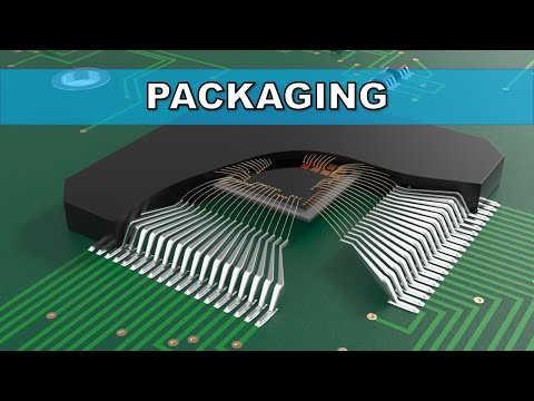
Optimizing SMD (surface mount device) packaging is essential for efficient assembly production and should be tailored to the SMT machine’s feeder types and quantities. There are four primary packaging options for SMD components, including tape, bulk, tray, and tube. For large-scale production, it’s best to use Tape Packaging. However, everyone recommends, for prototype or low-volume production, anti-static integrated circuit tube packaging. You cannot use Bulk packaging since it requires individual pickup or equipment for re-packaging.
Electronics demand meticulous attention to packaging. They are not only expensive and delicate but also susceptible to ESD. Hence, it is crucial to use protective packaging to safeguard against mechanical and physical damage during transportation.
In this article, we will cover all the essential information about packaging for electronics.
Importance of Electronic Component Packaging
Considering the factors above, it is evident that the electronic manufacturing industry. Faces significant challenges. Due to their fragility and high cost, any harm to electronics during transport can have severe consequences for both the financial standing and reputation of a business.
Static charges can also cause damage that may not be immediately noticeable. If a product does not power on, is not functioning right, or has a shorter lifespan than expected, it is likely that the packaging solution is to blame.
Hence, to achieve a successful packaging solution, it is necessary to ensure protection against effects during transit, moisture, mishandling, dust & static charges.
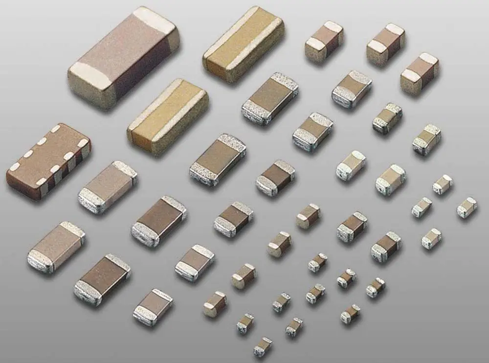
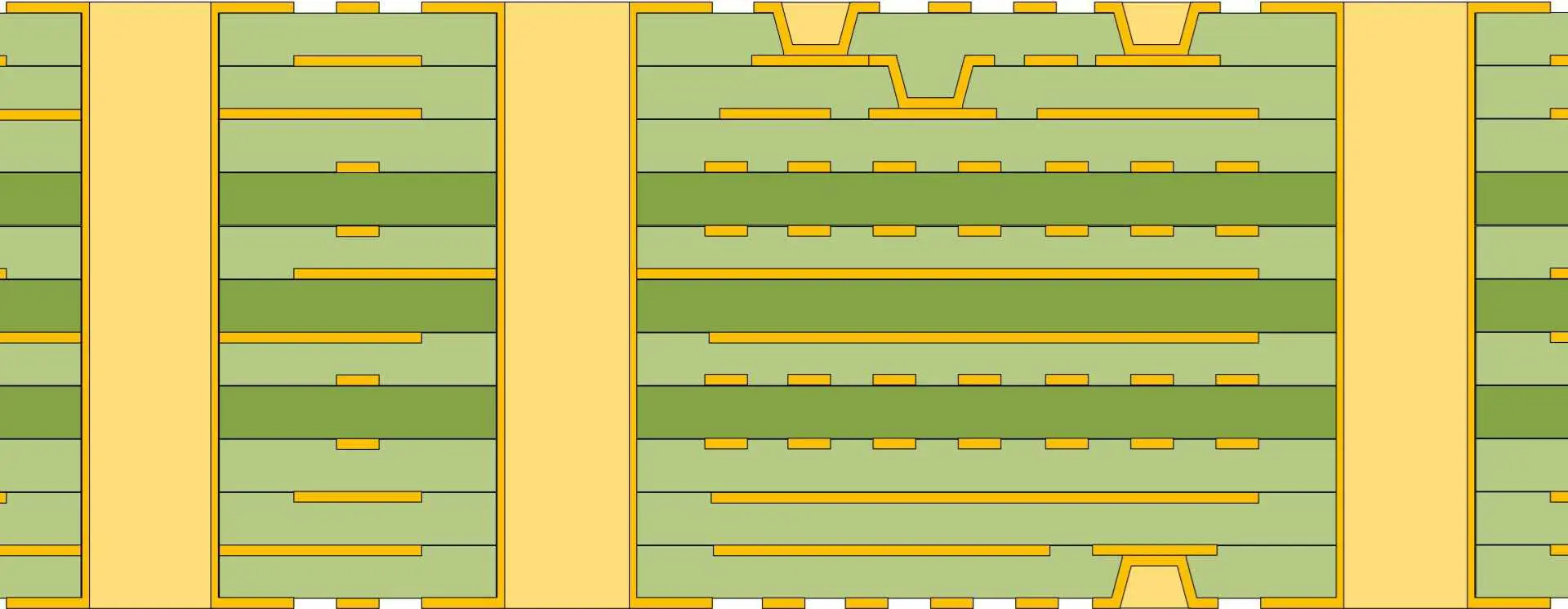
It is the most famous packaging form for electronic components. It is adaptable, efficient, and has been regularized. You can use this packaging form for all IC components except PLCC, QFP, & LCCC. Three kinds of tape are present in this packaging: plastic bag, paper tape & Surface mount tape. You can use this tape for packaging chip resistors and capacitors. Plastic bags are utilized for packaging several chip leadless elements, composite elements, special-shaped elements, SOP, SOT, Thin QFP, & other chip elements. You can use Carrier tape and reel packaging resistors, diodes, capacitors, transistors, Small ICs, crystal oscillators, and other patch components.
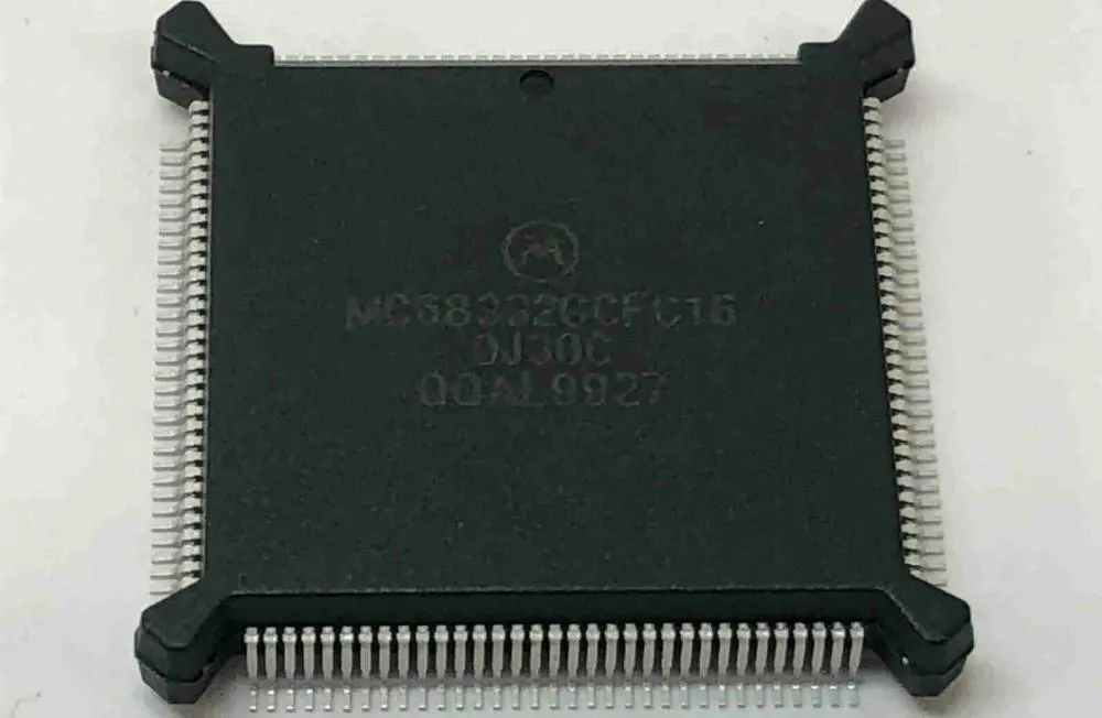
2. IC Tube packaging
You can use it for rectangular chip capacitors, resistors, small devices, and certain special-shaped components. It is ideal for situations with multiple SMT electronic elements in small batches. During packaging, manage the aspects in one direction & place them into the plastic tube. Next, insert stoppers such as plastic pins, nails, or rubber end plugs at all ends of a line & remove the cover of the SMT box. Then, following the mounting process, a chip element is fed to the substrate when the tube presses.
Tube packaging may have a higher cost for materials, and it may not be able to accommodate a large number of electronic components. Additionally, there is a risk of trapping elements in a confined space if the pressure is not evenly distributed. However, for SM integrated circuits, tube packaging is less expensive than tray packaging. However, it isn’t fast like the Carrier Tape packaging.
3. Tray packaging
Tray packaging divides a tray into the same parts using rectangular partitions according to cavities. It also places components individually into each hole, with an average of fifty pieces/tray. Once one is installed, then cover the tray with a protective film. There are Thermoformed Trays with single-layer, ten-layer, three-layer, twenty-layer, and twelve-four-layer tray feeders available. This method was initially applicable for high, medium & multilayer capacitors with larger shapes. Still, you can also use them for packaging elements such as QTP and SOP with many pins.
Tray packaging has two types: floppy trays and hard trays. You can use hard trays for packaging multi-pin and QTP components to prevent the wires from deforming. On the other hand, you can use Floppy trays for packaging common special-shaped elements.
4. In bulk
Bulk packaging encloses chip elements in the plastic box/bag without any particular arrangement. During mounting, one inserts a plastic box into a substance rack, and the components are fed into an SMT machine material port using the feeding tube. This method has a low cost and small size but a limited application scope.
Functions of Electronic Component Packaging
Electronic packaging design involves the integration of multiple small packages that work together to achieve a desired purpose. The packaging safeguards the printed circuit board & electronic elements from external damage. It also ensures that they do not interfere with the functioning of these elements. Nowadays, everyone views unpacking as expertise.
Packaging organizations (electronic) are under significant pressure due to the rapid evolution of electronic packaging design functions driven by technological advancements. As technology continues to improve, the demands on electronic packaging also increase and change accordingly. So it leaves these companies with the challenge of keeping up.
Two factors primarily derive from Electronics packaging: the rapid evolution of silicon IC (integrated circuit) technology and the continuous development of photonics. It is incorporated into different levels of interconnections for bespoke electronic packaging. It requires electronic packaging strategies to constantly adapt & modify their functions to keep up with the changing landscape of technology.
When it comes to photonic technologies, physically attaching these electronic elements to the printed circuit board raises the design to an advanced level. However, there is a physical connection between these components with other basic features in the system. It can pressure the schematic layout of packaging (electronic).
Electronics packaging design has several tiers, specifically Level 0 through Level 5.
Level 0 –At this tier of electronic packaging, the primary focus is safeguarding the chips & semiconductors, which serve as the fundamental and essential components of the electronic setup.
Level 1 –At this level of electronic packaging, the goal is to shield electronic components from damage.
Level 2 – The PCB is safeguarded at this level of electronic packaging.
Level 3 –At this level of electronic packaging, the assembly, boards & their related components are shielded and secured.
Level 4 – Modules or groupings of assemblies are safeguarded at this level of electronic packaging.
Level 5 – At this level of electronic packaging, a mixture of various modules and some electronic systems is protected and secured.
These levels enable electronic manufacturing firms to readily identify the necessary electronic packaging substances for a design, streamlining operations and increasing efficiency. By specifying the current electronic packaging tier they are working on, they can quickly locate the required components.
Top tips for Electronic Component Packaging
Ensuring the safety and security of a package must be the topmost priority, particularly when shipping fragile and valuable electronics. To avoid costly damages & returns, consider these simple tips.
Properly secure batteries for shipping – Numerous electronics rely on batteries, either integrated or detachable, for power. If not packed correctly, these elements can pose a significant risk of generating hazardous heat, fire, or sparks during shipping. To prevent such incidents, it is essential to safeguard all battery connectors against short circuits. One can achieve it by covering them with a non-conductive, insulating material.
Separate cords and accessories –In instances where electronics comprise multiple components, it is advisable to keep them well-organized within the package. Separating accessories and ropes can be highly beneficial for the user, as it prevents tangling, enables appropriate labeling of each component, and enhances the overall customer experience.
Use effective shipping materials – Choosing the appropriate materials is crucial to ensure your electronics reach immaculate condition. Void fillers, & antistatic products are some options you can use to safeguard your products. You can keep them secure during transportation.
Deter and detect damages – Electronics are susceptible to damage during transit, which can be detrimental to your business due to their fragility and high cost. However, by utilizing impact signals, you can mitigate & detect defects during shipping to prevent losses. ShockWatch labels have an excellent Tamper-evident solution. You can apply it directly to the package. They act as a visual deterrent for package handlers and provide physical proof of impacts between five and seventy-five by releasing red dye. To learn more about impact indicators, refer to this recent case study in which these labels maintain high-tech devices in a new situation.
If your company deals with the production or shipping of electronic components, then you understand the importance of protecting these elements during storage & transportation. Electronic parts are extremely susceptible to harm caused by oxygen infiltration and other corrosive elements present in the environment.
· Packaging Challenges
Selecting the appropriate packaging for electronic components that you can rely on can be a challenging undertaking. Buying unsuitable packaging can result in expensive waste & damage to your organization’s reputation. Therefore, you will undoubtedly want to take all necessary measures to safeguard your enterprise assets.
Moreover, electronic components come in various sizes and shapes that are often irregular, making it challenging to find suitable packaging solutions that can effectively protect them. It is not easy when safeguarding electronic elements & electrostatic discharge, as the appropriate packaging options are more limited.
· The Solution
Aluminum laminate foil packaging can protect your electrical elements against corrosion during storage or transportation. Whether an entire machine or a motherboard, this packaging option can safeguard your equipment. But what sets it apart from other packaging materials?
Make sure the PCB or Circuit Board you employ in the projects will function properly and satisfy your customers. It’s critical to possess a reliable method for checking PCBs for faults and making sure they work as intended.
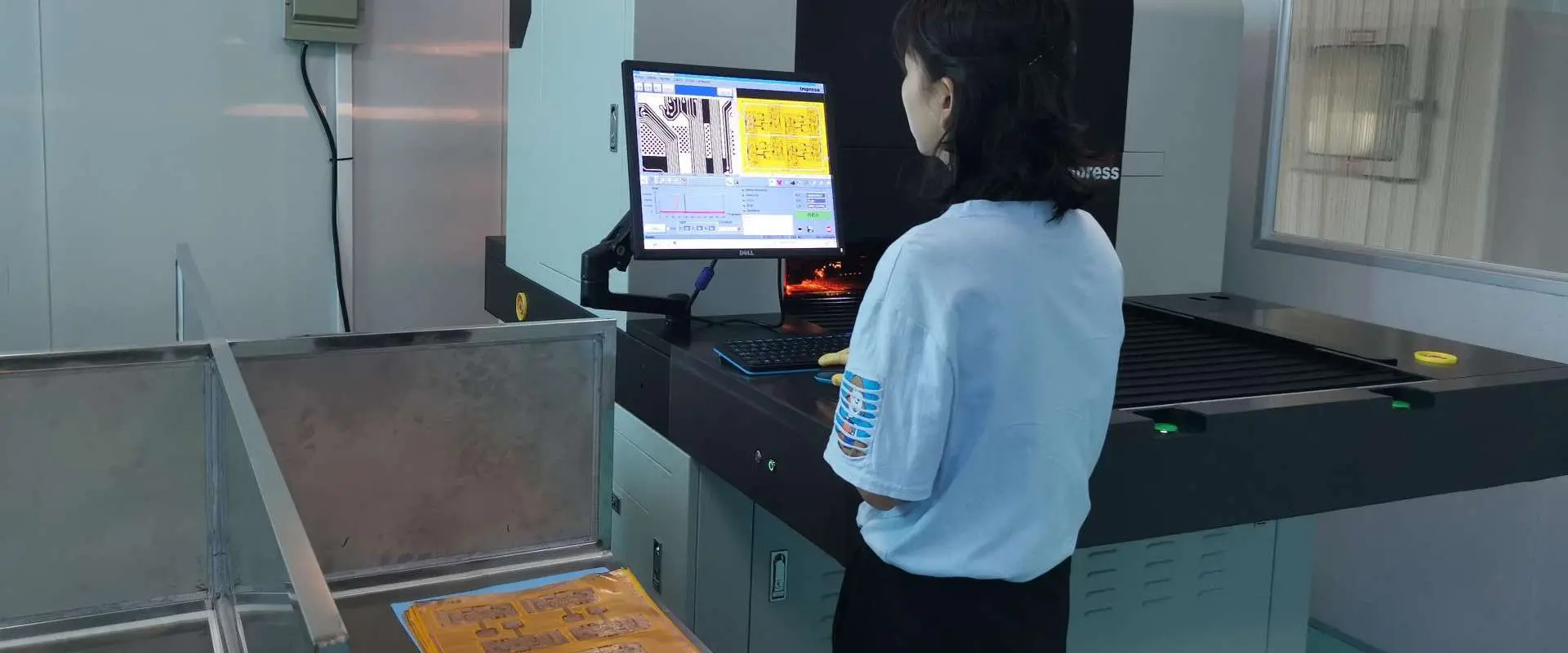
The size and complexity of PCBs are both increasing; today’s PCBs can contain numerous soldered joints with a huge number of microscopic components. Errors may occur more frequently as a result of the increased complexity. Automated optical inspection or AOI approaches can give more clarity and accuracy when a typical visual examination is unable to discover minute flaws in a crowded, tightly packed board.
How can one define AOI? The Automatic optical inspection involves an electronic scanner that employs light imaging to visually check the finished PCB. It assesses the level of craftsmanship to ensure that the Circuits are appropriate for usage and purchase.
A typical AOI system includes several light sources, numerous cameras, and maybe even video cameras. Several light sources from various perspectives illuminate the Circuit board. Moreover, the cameras click videos and photos to produce a complete image for analysis.
Without the requirement for a manual visual inspection, AOI measurement often employs a scanner to autonomously scan the item. The scanner checks for larger problems that would impair the quality of the PCB as well as tiny errors that might result in catastrophic failures, like the lack of a crucial component. Smaller flaws include things like slightly misaligned parts and soldering that creates the incorrect shape or size.
At several phases of the production process, AOI is helpful. It performs well for the inspection of solder paste, bare PCBs, and pre and post-reflow. Each step has the potential to create design flaws in a PCB, and AOI aids in identifying these flaws before production on a defective board continues.
Although, the majority of AOI happens during post-production. This is because the AOI may employ an individual system to simultaneously examine several types of faults. One thorough inspection takes relatively less duration than one inspection after each stage of the procedure. Utilizing AOI for a final verification allows the production process to move quickly and enables it to meet deadlines and higher productivity. Additionally, the problematic boards also go back for repair while the remaining boards proceed if AOI discovers faults during the post-production phase.
The Role Of AOI Machine
PCB manufacturing depends significantly on AOI. It ensures that every board can deliver the high efficiency needed in intricate electrical devices.
When AOI finds a PCB defect, it marks the PCB and sends it back for rework. This procedure may take place in a number of distinct manners. The results of the AOI may not meet some facility specifications, such as all the PCB lines ought to be larger than a particular size. In this situation, people may examine the results and choose which boards need repair. AOI can make a comparison between the actual PCB and a CAD rendering of an ideal PCB. When the real PCB diverts from the desired design, AOI automatically spots those areas and flags the PCB for reworking.
For PCB manufacture, AOI offers the following advantages:
· Ensuring Quality
You may use AOI to verify that the PCB products work as planned. Increasing customer happiness, improving your company’s reputation, and giving clients assurance about the service quality you’re providing all benefit from maintaining the PCB quality.
· Evaluating A Complex Board
A board from Millennium Circuits will automatically go through AOI if it has over 100 components. The naked eye is incapable of inspecting complex PCB layouts with the same level of precision as AOI.
· Improving Processes
If flaws occur from defective processes, grasp them right away using AOI. AOI may assist you in identifying defect patterns and modifying your procedures before producing thousands of PCBs with the same defect. According to the latest study, finding a flaw in a PCB that has just been assembled is just ten times more expensive than finding one in a bare PCB. Yet finding a flaw in a PCB that has already been put to use in the field is around 1,000 times more expensive. Early mistake detection reduces the possibility of future repair and improves the productivity of your manufacturing processes.
· Customizability
Even though AOI operates fully automatically, the operator may still specify the parameters that will inform the scanner where and what to look for. It’s simple to tweak your parameters to locate the defects you need if the design requirements change.
The following constitute a few of the elements evaluated while an AOI:
Soldering Defects
Soldering employs a very low-melting-temp alloy, frequently lead, lead-free or tin alloy, to bond the PCB’s electrical components. With the exception of not melting the electrical components, the procedure is comparable to welding. When the bonds between two electrical components don’t form properly, this is known as a soldering fault.
The following are some typical soldering flaws that AOI might look for:
· Open Circuit
PCB’s open circuits are typically the main problem. The reason is that an incomplete or open circuit stops the current from passing through them. The board won’t operate properly if a circuit is wide open.
Open circuits may arise due to inadequate traces or vias. These improper traces form due to inefficient soldering. An evident open circuit may occasionally be found by eye examination, while AOI can find even marginally open circuit points and mark the PCB for correct circuit closure.
· Solder Bridges Or Solder Shorts
Solder bridges happen when two PCB components are connected electrically, even though they shouldn’t be. These bridges may develop if a board is produced with an excessive amount of solder or if solder leaks into a solder-free section of the PCB.
If the solder paste fails to detach from its tips or leads prior to solidifying, solder bridges frequently happen. The metal pads known as leads are used to link two places on a circuit board. Due to the size of the leads, the amount of paste bonding them to a PCB, or the shallow pitch of the PCB, the solder paste may not separate.
Solder bridges cause problems as they hinder the desired current flow through the circuit. They may short-circuit the PCB or destroy vital components or vias. Additionally, solder bridges are extremely hard to spot with the human eye; even minute solder seepage may allow them to develop. Luckily, AOI scanning may detect even the smallest solder bridges or shorts and return the defective circuit boards for correction.
· Insufficient Solder
When the manufacturing process utilizes insufficient solder to bind various components onto the circuit, an inadequate solder connection develops. Solder skips happen when the solder occasionally fails to join the components completely.
The PCB’s performance will suffer if the connections of components are improperly soldered because they may not produce solid electrical connections. Additionally, the PCB will have missing parts if there is insufficient solder to hold the electrical components in place, which will very certainly lead to catastrophic failure. If a board has to be resoldered, an AOI may scan it, note how much solder is on each electrical component, or compare it to the right picture.
· Excess Solder
When the reverse occurs, that is, when the manufacturing process soldiers the board, excess solder results. Sometimes it happens as a result of using too-wide soldering tips or applying too much heat.
Solder bridges and other defects like excess solder might be problematic. A huge spherical solder ball may form when excessive solder is applied to a board pin during production, making it hard to determine if the board pin is adequately moistened to adhere to the PCB.
Due to their size, solder balls or bridges are generally simple to spot, although a human examiner may skip one after examining hundreds of almost similar boards. With the use of a solder wick or solder sucker, an effective AOI scanner may quickly identify excess solder and return the board for repair.
Component Defects of AOI Machine
Defects in the tiny functional elements connected to a PCB are known as component defects. Here are a few typical PCB component flaws:
· Lifted Lead
When one small metal pad on a circuit doesn’t stick correctly, the lifted lead results. Sometimes a raised lead happens as a result of manufacturing handling, extreme heat, or board flexing. On the other hand, it happens when leads that are excessively long rise once they touch solder.
The instability of lifted leads makes them troublesome. Pins may link to a copper sheet below using the metal pads on the PCB. However, if somehow the lead rises, the pins won’t allow it to do so correctly. Missed connections may harm the operation of the board and lead to component failure.
· Missing Components
A Circuit board may miss an electrical component due to various causes. Inadequate soldering may result in components going missing, or the manufacturing process may omit a crucial component.
A PCB with a missing electrical component has a major fault that might result in catastrophic failure. The naked eye may see the missing part. Yet, since this is a serious flaw, having a trustworthy AOI scanning device is essential for identifying the missing components in PCBs before they reach end users.
· Misaligned & Misplaced Component
Misplacement or Misalignment can happen when the manufacturing process installs components wrongly or when electrical components move after placement. Due to the ease with which parts can move on top of molten solder due to the solder’s low surface tension, component shifting often occurs during reflow.
The PCB may function even with a misplaced or misaligned component, although it may operate slowly. Or it may not function at all. The ability to detect alignment issues requires a reliable AOI scanner since some alignment issues may be too little to be seen with the human eye.
Comparing AOI Machine With Other Inspection Methods
AOI offers a number of benefits over other procedures for finding PCB flaws. A comparison between AOI and other inspection techniques is described below:
1. Automated X-Ray Inspection (AXI)
Instead of using light scanning to check the PCBs, AXI employs X-rays. AXI is frequently used by businesses to assess boards with especially intricate or thick construction. This is because X-rays can photograph the materials since they pass through them. One component could be able to block others since the light utilized for AOI bounces off surfaces. But an X-ray passes through several layers of substance, precisely imaging each one.
AXI features brand-new, cutting-edge technology, and its biggest drawback is the cost. AXI seems so expensive that, unless a board is exceptionally complex or densely packed, it is frequently not worthwhile to utilize.
2. Automatic Laser Test (ALT) Measurement
Instead of using conventional light imaging, ALT measurement scans and measures PCBs using lasers. The ALT technology uses the placement of the lasers to determine the height and positioning of various components and evaluate their reflectivity when the laser bounces off the components of the PCB. Similar to AOI, the ALT technology may identify any defects by comparing the empirical analysis to a list of requirements or schematic.
Although interference can occasionally result in erroneous results, ALT technology is particularly helpful in determining where and how much solder paste is present.
3. In-Circuit Testing (ICT)
An electric probe is used in in-circuit inspection to assess the performance of a built PCB. Each component’s placement and functionality are checked using a current of electricity. It examines crucial electrical properties, including resistance and capacitance, as well as checks for open and short circuits.
ICT seems to provide less comprehensive soldering data than AOI since it relies on electricity rather than imagery. It can assess the caliber of components and offer details on circuitry-affecting soldering flaws, but it is unable to provide much information regarding inadequate or excess solder.
Particularly for the thinner PCBs being created today, AOI is typically more trustworthy than in-circuit inspection.
4. Manual Visual Inspection (MVI)
Since AOI doesn’t involve touching the PCB, most PCB businesses prefer it to human visual examination. The human examiner must examine the PCB. Moreover, handling may cause an otherwise flawless board to develop flaws. AOI also helps in maintaining PCBs’ structural integrity and scanning their sensitive components without harming them.
A more trustworthy method than a personal visual assessment is AOI. A person may overlook the tiny PCB fault. However, AOI can detect even the smallest mistakes. It can easily scan the PCB in more detail than a human eye is able to see. It is dependably trustworthy throughout all phases of the production process. Its relentless acuity never wanes.
Conclusion
Verifying the PCB’s quality as they leave an assembly line is crucial. This allows for the monitoring of the boards’ quality as well as the early identification and correction of errors to avoid recurrence.
This also shows the significance of an AOI system for a fabrication organization.
PCBs are an essential component in electronic applications, making performance, reliability, and safety-critical factors to consider. To ensure these aspects, engineers must comprehend how temperature impacts the quality of their printed circuit board assembly during the development phase, even before PCB creation begins.
PCB design comprises several components like holes, traces, solder masks, layers, and through holes, each susceptible to heat. Elevated temperatures can have negative consequences on standard PCBs, as well as any other type of PCB. The PCB’s element determines its maximum temperature, known as the printed circuit board temperature limit.
What is the typical temperature range for PCBs? The temperature range of a PCB is measurable by the material, resulting in variations in the temperature limits for different PCBs.
FR-4 is the most prevalent substrate useful in PCBs, comprising a flame-resistant glass epoxy substrate. It can endure temperatures ranging from 90°C-110°C.
High-temperature printed circuit boards are typically categorized as those with the Tg exceeding 170°C, although some may use 150°C as the threshold. The specific definition may differ among high-temperature printed circuit board manufacturers.
It is important to consider thermal expansion before checking the temperature range of your PCB. Temperature monitoring is critical for identifying hot-power areas and power-hungry ICs and making necessary adjustments or corrections early.
Ensuring that the CTE aligns crucial if your printed circuit board has greater than one layer. CTE measures the expansion of materials at high temperatures. The dielectric layers must have a similar CTE to the copper coatings. If they are not together, each layer will expand at multiple rates, which can cause serious issues.
Measuring PCB Water Temperature
Before determining the maximum operating temperature of your PCB, there are some factors that you should consider.
No need to rewrite this sentence as it is already clear and concise.
Ensure the printed circuit board temperature indicator is installing properly before checking the temperature.
Locate the ground pins, which should be with the laminate of the primary heat source. These ground pins facilitate the transfer of around 60 to 65 percent of the generated heat to the temperature sensor. Since the ground pins are with the laminate, they also have a minimum thermal resistance than other components among the heat source and the sensor.
Join the ground pins of every temperature gauge to the ground plane of the heat source.
Maintain proximity between the heat source & temperature sensors.
Acceptable temperature boost for a PCB trace
The mechanical stability of the base material of a PCB becomes compromised at the glass temperature (Tg). It is important to note that the printed circuit board’s Tg is less than its melting point.
Each PCB has a unique glass transition temperature (Tg) based on its substrate. When the operating temperature exceeds the glass transition temperature, the printed circuit board’s mechanical stability becomes compromised. PCBs with a greater Tg value have improved stability at elevated temperatures because their substrates offer good heat resistance, chemical stability, and mechanical stability.
It is recommended that the Tg value of your PCB should be 20°C-25°C greater than the anticipated functional temperature of the equipment you are designing for. For example, if your PCB’s Tg value is 130°C, the device’s functional temperature must be less than 110°C.
PCB Water Temperature copper traces
Copper traces generate heat due to power dissipation from I2R, where I is the current and R is the trace’s resistance. The heat is then dissipated through the base material by thermal conductivity, radiation, and convection. The PCB temperature will stabilize when the heating or cooling costs are equivalent.
The copper trace current capacity is influenced by various factors, including the highest temperature rise needed and the trace width.
The trace width of a PCB depends on various factors, including the resistance, current flow, and the maximum temperature increase that can be tolerated.
Usually, a temperature increase of up to 10°C above the average temperature of twenty-five-degree centigrade is acceptable. However, in some cases, a temperature rise of up to 20°C may be permitted if the PCB design and material allow it.
What happens if the PCB Water Temperature drift is too high?
If the temperature rises in your PCB’s copper trace is too high, such as 50°C or 100°C, it can negatively impact nearby components’ ambient temperature, leading to decreased board integrity and power loss. While a copper trace on a FR 4 board may be able to handle such a temperature rise, it’s still important to consider the potential consequences.
There are several reasons whyPCBs may experience high temperatures; some of the most usual include:
· Malfunction causes heat dissipation
If a component malfunctions on your printed circuit board, it can lead to heat dissipation. The faulty component can no longer create high power, which causes nearby components to work more to compensate and generate more power. This results in the generation of more heat.
· Through-hole interference
Through-holes provide electrical connections among the layers through electroplating in the plated holes. The heat sink elements and through-holes are responsible for the power supply. However, if the heat dissipator doesn’t connect properly or if there is any obstruction with the PTH due to other components, it causes nearby elements to work harder, leading to the generation of more heat. This, in turn, leads to the maximum temperature.
· Lead-free solder
The use of lead in electronic applications is a hazardous material and increases challenges to health and environmental safety. As a result, design engineers globally comply with the EU’s RoHS by limiting the use of lead solder. However, the lead-free alternatives often have a higher melting point, resulting in PCBs requiring higher temperatures to operate, leading to increased stress on components.
· The distance of your surface mount
Proper distance between through-hole components and surface mount devices (SMDs) ensures a smooth current flow via a through-hole and heatsink. If placed too far apart, the current has to travel farther, resulting in cooling time for the receiving components. This can cause other components on the circuit board to create more power to compensate, ultimately leading to overheating.
· External thermal issues
It is important to consider the operating environment of the PCB and its components during the design phase. Neglecting this can lead to thermal stresses on the board in both high-temperature environments and extremely low. Resistors, capacitors, and semiconductors are among the components that can be affected by temperature changes.
· High-frequency circuits
High-frequency circuits are prevalent in mobile, microwave, high-speed design applications, and radio frequencies like smartphones. However, the downside is that these circuits tend to produce more heat due to the power they require. As a result, higher temperatures are inevitable in such boards.
There are several common methods for preventing temperature enhancement in PCBs.
To ensure high-performance PCBs, it’s essential to control heat through effective design. If the circuit board will be exposed to extreme temperatures, such as high or low environments, it’s crucial to consider this during the design phase. Follow these tips to maintain the optimal temperature of your PCB.
· Use heat sinks
Effective heat conductivity is crucial in controlling heat for high-performance PCB design. Heat sinks, typically made of aluminum or copper due to their outstanding thermal performance and low thermal resistance, are attached to components such as high-power transistors on the board to absorb and disperse heat in the air. The heat generated by the components is naturally transferred to the heat sinks.
· Choosing the right materials and components
Effective PCB design relies on using high-temperature-resistant materials. PCBs with thick copper plates are capable of withstanding high temperatures, which can extend the lifespan of the application. In contrast to conventional PCBs, these boards can handle elevated current levels, resist high temperatures for longer periods, and provide stronger connection features. The most commonly used material for PCBs is FR4, which is a glass epoxy that can tolerate high temperatures. Additionally, high-frequency elements like PCB laminates can provide outstanding dielectric attributes at various frequencies. When selecting a laminate, it is important to choose one that can absorb moisture and withstand high temperatures.
· Adequate Spacing
To prevent any interaction between the segments on your circuits, it is important to ensure sufficient space between them. Failure to do so could result in heat generation caused by the interaction between the components. By maintaining a distance between them, such issues can be avoided.
FR-4 PCBs typically endure temperatures as low as -50°C, beyond which brittle cracks may develop in the element. However, it’s advisable to avoid subjecting your FR-4 PCBs to extreme temperatures to reduce stress and extend their lifespan. In industries like aerospace, where PCBs may be deployed to outer space, they may be exposed to temperatures as low as -150°C, well below the recommended limit for the FR-4 printed circuit board.
Applications Of PCB Water Temperature
Thankfully, one can use several alternative materials instead of FR-4 to fabricate PCBs that require high-temperature resistance. One such material is polyimide, which can withstand a wide range of temperatures, including cryogenic conditions and temperatures as high as 260 Celsius.
Additionally, polyimide materials are highly resistant to fire. While polyimide materials offer excellent temperature resistance, they are vulnerable to water, making them a crucial factor to consider during the design phase.
Ceramic PCBs, on the other hand, are a more expensive option that offers the advantages of both worlds. These boards can withstand extreme temperatures, both low and high, and are impervious to water.
However, the high cost and design constraints with ceramic circuit boards are their downsides. In conclusion, there are meaningful differences or benefits among ceramic printed circuit boards. One should evaluate FR-4 circuit boards & MCPCBs evaluated for each application.
Due to its exceptional conductivity at or -272°C, aluminum holds great value in cryogenic printed circuit boards. However, the drawback of using aluminum is its high reactivity, which necessitates unconventional techniques for constructing circuit boards.
Something that is considered ordinary or usual is referred to as a standard because it acts as a yardstick by which other things of a similar nature may be compared. As an example, Apple has always been regarded by many as the pinnacle of the mobile market for quite some time.
Size is another definition of a standard. For instance, refrigerators typically range in width from 24 to 40 in. The standard serves as a crucial consideration when examining an object’s dimensions since it specifies what features and functionalities the product must have.
PCB thickness serves as a crucial guideline to take into account if you want to concentrate on PCBs. There doesn’t exist an official and definitive standard, though, which needs to remember always. However, as they refer to the most popular choice and are often available, some typical sizes are regarded as the norm.
Your manufacturer will often suggest that you adhere to those approved standards of PCB thickness so that your design may be adjusted to the equipment’s capabilities you’re utilizing and to save turnaround time and cost for the PCBs.
In this article, we talk about common standards of thicknesses PCB and show you exactly how to specify them. We also go through the factors that need to take into account when deciding between the standard and non-standard specifications, as it is a crucial design decision.
The typical PCB thickness, according to manufacturers, is 1.57 mm, or around 0.062 inches. That is both somewhat right and partially incorrect. The reference size has been 0.062 inches since that is the bakelite layers size that was produced in the beginning days of Circuit board production. Actually, it’s merely a matter of historical precedent.
These days, PCB can be built smaller or bigger than the PCB standard for thickness. But for the majority of designs, that standard is still the most often chosen alternative. The existing standard really exists on a spectrum, to be precise. Three popular standard thicknesses of PCB are available: 0.78mm (0.03 in), 1.57mm (0.062 in), and 2.36mm (0.093 in).
A multitude of manufacturing and design considerations must take into account to choose the proper PCB thickness. The following design elements must consider while choosing:
Over time, multi-layered board designs have evolved and have become a common kind of board utilized in PCB manufacturing. They frequently comprise copper-covered glass cloth with an epoxy foundation. Technology advancements have made it possible for the multiple layers to support greater weights while maintaining a 63mm thickness.
Complex circuit wiring demands led to an increase in circuit board layer counts. As a result, the PCBs that were produced as well contain more layers, which causes the Circuit thickness to rise from 63mm up to 93mm.
Internal layer cores with thicknesses of 93, 59, 47, 39, 35, 28, 21, 18, 14, 9.5, 8, and 5 mils are available using Isola’s 370HR materials. For materials with high-temperature, there are various options of thickness, such as 39, 22, 14, 10, and 8 mils, available for cores of Isola’s 370HR.
The number of foil lamination layers affects the conventional PCB thickness as well. The typical thickness for foil lamination on a four-layer circuit board would be about 0.031.” The most suitable standard thickness for a six-layered foil lamination is about 0.062.”
Finally, the typical Circuit thickness includes 0.125, 0.093, and 0.062 inches for an eight-layered or a tenfold-layer board. Depending on the needs of your PCB, you may also select an internal copper foil layer that is 12, 1, or 2 ounces thick. Moreover, You can utilize your own stack-up or one of the dielectric builds we’ve supplied.
PCBs consist of sheets or panels in standard sizes. This indicates that they are produced in conventional sizes, which explains why the fabrication companies probably already have them on hand or can rapidly obtain them.
Other sizes could be possible, but they may constrain by the contract manufacturer’s equipment processing capacities, and obtaining customized PCB thickness will add to the delay.
Therefore, sure, you may have a customized PCB thickness. However, this will rely on your manufacturer, and you must account for a delay. This is because it takes longer to obtain these customized panels or sheets.
If your layout calls for an unusual PCB thickness, you must take it into account. If you are looking for a customized PCB thickness, there are some other elements to take into account; we will go over them in more detail in the next section.
Factors To Consider When Ordering Custom Thickness of 0.093 Inches
1. Equipment Capabilities
The most crucial element to take into account is this. Ensure that your manufacturing facility has the tools necessary to produce PCBs with the desired thickness. This and other crucial design decisions must create early in the design phase to avoid having to revise and rethink your whole PCB layout.
2. Longer Turnaround Time
The turnaround period will become longer if a rare Circuit thickness is needed since it takes longer to prepare the panels. Due to its potential to disrupt your timetable and have an influence on the prototype stage, this ought to be taken into account immediately.
3. Greater Cost
Choosing a customized PCB thickness can result in more costs due to the potential need for specialized materials, more work and labor hours, and manufacture, as is frequently the situation with bespoke products. To determine whether you can handle the added expenditures or not, you must examine this from the start.
A bespoke PCB thickness makes more sense in certain situations, while the conventional Circuit thickness is an excellent choice in others. Therefore, the decision is ultimately up to you. You may reduce your expenses and have quicker turnaround times by using standard Circuit thickness. If you want to go with a customized PCB thickness, you must find a fabrication facility with the appropriate tools.
You’ll be glad to learn that RayPCB has an extensive network of PCB manufacturing facilities all around the globe that can accommodate any project needs. Every shop offers a lot of experience, many quality certifications, and cutting-edge tools. We’ll be able to adhere to your instructions and construct your boards accurately the very first time.
All of the PCB assembly processes are in-house. We prioritize DFM to minimize turnaround duration and ensure that you don’t need to spend time making back-and-forth design revisions. All of the components are acquired from reliable vendors. Additionally, we offer complete assistance throughout the whole procedure. Beginning with design, enabling us to produce a seamless transition from the stage of prototyping to production.
We know for offering efficient, excellent PCB fabrication that will satisfy all of your demands. In contrast to other businesses, we devote our whole time to comprehending your design and objectives so that we can assist you in deciding between the standard and customized PCB thickness.
Are you ready to delve into the world of electronic hardware design? As an electrical engineer, you will create the electronic components and systems that power our everyday products. From consumer electronics to medical devices, automotive systems, aerospace and defense applications, industrial automation, and renewable energy, electrical hardware design plays a massive role in our lives. In this article, we will learn about electrical hardware design use cases, potential challenges designers may encounter, and the tools required to become a competent electronic hardware designer. So, let’s get started!
Electrical hardware design entails Creating a comprehensive schematic or diagram that depicts the physical architecture and connections of electronic components and systems. In addition, the procedure involves the creation of electrical circuits, selecting suitable parts, and integrating them into a system that meets specific performance requirements.
Use Cases of Electrical Hardware Design
The following are the areas in which electrical hardware design is applicable:
1. Consumer Electronics:
Consumer electronics are the most common use case for electrical hardware design. Electrical engineers play a crucial role in designing the electronics that power these products, from smartphones to smart home devices to gaming consoles. Electrical hardware design impacts everything from the performance and reliability of these devices to their safety and compliance with regulations. For example, electrical engineers must design circuits and power supplies that can handle high-performance computing demands while ensuring that the device is safe and compliant with regulations.
2. Medical Devices:
Another significant application for the creation of electrical hardware is medical devices. Electrical engineers create the electronics that power these devices, allowing them to carry out essential medical functions, including imaging equipment, surgical robots, and pacemakers. Medical gadget reliability and safety are of utmost importance, and proper electrical hardware design is essential to ensure these devices work as intended. Electrical engineers, for instance, must create circuits that can precisely monitor and react to physiological signals while ensuring the device is secure and compliant with rules.
3. Automotive Systems:
Electrical hardware design is crucial in the field of automotive systems as well. Electrical engineers create the electronics that power these systems, allowing them to carry out essential functions in everything from engine control systems to driver assistance features to infotainment systems. Safety and reliability are critical in automotive systems because any malfunction or failure could have detrimental effects. Everything from a vehicle’s emissions and fuel economy to the occupant’s safety and comfort can be affected by the architecture of its electrical hardware.
4. Aerospace and Defense:
Another application field where electrical hardware design is crucial is aerospace and defense. Electrical engineers create the electronics that fuel these systems and give them the ability to carry out essential functions in satellite communications, missile guidance systems, or aircraft avionics. Reliability and performance are crucial in aerospace and defense uses, and electrical hardware design is essential to ensure these systems work as intended. Electrical engineers, for instance, must create circuits that can endure high temperatures, shock, and vibration while ensuring the system is secure and compliant with laws.
5. Industrial Automation:
Electrical engineers design the electronics that power these systems, allowing them to carry out essential functions in everything from manufacturing robots to process control systems to power distribution systems. Reliability and efficiency are critical in industrial automation apps because downtime or inefficiency can negatively affect output and revenue. In addition, the electrical hardware architecture can affect everything from these systems’ power consumption and efficiency to their safety and regulatory compliance.
6. Renewable Energy:
Electrical engineers create the electronics that allow these systems to collect, store, and disseminate renewable energy, whether in solar panels, wind turbines, or energy storage systems. Efficiency and dependability are essential in renewable energy because any energy loss or downtime can affect the system’s viability. The electrical hardware architecture can impact everything about these systems, including their productivity and output, as well as their safety and regulatory compliance.
7. Internet-of-Things
Electrical hardware design is essential in the development and implementation of Internet-of-Things (IoT) devices. The integration of different components such as sensors, microcontrollers, communication modules, and power management circuits requires careful consideration to ensure the device’s proper functioning. Electrical hardware designers need to consider factors such as power consumption, data transfer rate, sensitivity, accuracy, and communication range when designing IoT devices. Sensors are responsible for collecting data, microcontrollers process the data, communication modules allow the device to connect to the internet, and power management circuits ensure the device operates within the specified voltage range.
Potential Challenges when Designing Electrical Hardware
hardware development
There are numerous difficulties that designers may need help with when designing electrical devices. The following are a few of the most typical problems:
1. System-level Requirements
Electrical systems can be intricate and comprise several subsystems, each with its own needs. Customers or end users usually define the system-level requirements, including functional, performance, and legal requirements.
Electrical hardware designers must thoroughly grasp the system architecture, subsystems, and individual components to meet the system-level requirements. To achieve the intended functionality and performance, they must ensure that every element complies with the needs and functions flawlessly as a unit. When building the system, the designers must consider aspects like electricity consumption, heat dissipation, and electromagnetic interference (EMI).
2. Component Acquisition
A further difficulty in designing electronic hardware is finding the required parts. Multiple vendors frequently help obtain electronic components, and each has its own wait times, costs, and stock levels. Furthermore, the market for electronic components is continuously changing, with the introduction of new elements phasing out of outdated ones.
Therefore, electrical hardware designers must study the electronic components market and keep up with the most recent technological trends to meet this challenge. Additionally, they must build relationships with dependable vendors and have backup strategies if a component stops working. Finally, the designers must also closely consider the cost of each element and balance it against the system-level requirements.
3. Computer Design Requirements
In addition to meeting the system-level requirements, electrical hardware designers must ensure that their designs meet the computer design requirements. This encompasses elements like EMI, heat dissipation, and power consumption. These requirements are fundamental in designing embedded systems since they usually have constrained power and thermal budgets.
Therefore, designers must meet the specifications for computer design to overcome this challenge and use specialized tools and methods to optimize their designs. These tools can include thermal and power usage simulation tools and EMI analysis tools for locating and reducing possible interference.
4. Life-cycle Support
Once an electrical hardware design is complete, it must require support throughout its entire life cycle. This necessity includes activities such as manufacturing, testing, and maintenance. However, life-cycle support can be challenging due to component obsolescence, changing regulatory requirements, and the need for ongoing testing and validation.
Therefore, electrical hardware designers must consider life-cycle assistance when creating their systems to overcome this difficulty. This action will entail choosing components with wide availability and a long lifespan and designing the system to be simple to manage and upgrade. In addition, the system must continue to meet the desired performance and usefulness, so the designers must stay current on regulatory requirements and frequently test the system.
5. Design Culture
The design culture encompasses the company’s general design ethos, communication and collaboration procedures, and design methodologies. In addition, an influential design culture can facilitate innovation, while a weak one can inhibit it.
Companies must cultivate a strong design culture promoting cooperation, innovation, and ongoing development to meet this challenge. This step may entail creating clear communication channels, supplying designers with training and development chances, and promoting the application of best practices and standardization.
6. Business Model
Finally, the business model can also present challenges in electrical hardware design. These are factors such as market demand, pricing, and competition. Electrical hardware designers must ensure that their products are available at a reasonable price while still providing the desired functionality and performance.
To overcome this obstacle, businesses must closely examine consumer demands and market trends to create goods that satisfy the market. Therefore, they can involve conducting market research, getting a firm comprehension of the competitive environment, and making pricing plans that balance profitability and cost. Companies also need to ensure that their designs are competitive in terms of both material and manufacturing expenses.
Many tools are available to assist with the electrical hardware design process, making it easier and more productive for designers to complete their work. The following are some of the most typical tools used in the creation of electrical hardware:
1. Elecdes Design Suite (EDS):
Elecdes Design Suite (EDS) is a software program created especially for electrical engineering and electronic design. It offers schematic capture, component libraries, and automatic wire routing tools for making electrical and electronic systems. In addition, EDS can produce a few records, such as the Bill of materials (BOM), wiring lists, and cable schedules.
In addition, EDS is an effective instrument for designing electrical hardware because it accelerates design and lowers error rates. By automatically routing wires, it prevents short circuits and other problems and ensures they have the correct routing. Additionally, designers have access to various components thanks to EDS’ component libraries, which improves precision and saves time.
2. Siemens Software
Siemens offers software tools for designing electrical hardware, such as Solid Edge Electrical, specifically for creating electrical hardware, and NX Electrical Routing, a tool for routing electrical wires and harnesses. These software tools offer creators a variety of features, including automated routing, 3D modeling, and schematic capture.
Schematic capture, electrical design rule checking (DRC), and wire and harness design are just a few of the many tools offered by Solid Edge Electrical for electrical design. Additionally, it has a collection of electrical symbols and parts that can change shape to fit specific design specifications.
NX Electrical Routing is a 3D tool for routing electrical wires and harnesses. It gives designers the tools to make electrical cables and harnesses, change them, and automatically route them through 3D models. Advanced features like wire flattening, which enables designers to view and alter cables and harnesses in 2D, are also present in NX Electrical Routing.
3. Wire Cutters
You often require wire cutters to trim and strip wires when designing electrical components. There are diagonal cutters, needle-nose forceps, and wire separators among wire cutters. The diagonal edge is a wire cutter for severing wire and cable. They cut wire with minimal force and can cut it up to a specified gauge.
The function of needle-nose pliers is to manipulate and secure the wire. They are typically helpful in areas inaccessible to other instruments.
Wire strippers help remove the insulation from electrical wires. They are available in various diameters and can separate wires of multiple gauges.
4. Pliers
Pliers are versatile instrument that is applicable for a variety of duties in the design of electrical hardware. They help grasp, bend, cut, and strip wire. There are numerous varieties of pliers, such as needle-nose pliers, lineman’s pliers, and slip-joint pliers.
Needle-nose pliers have long, pointed jaws. They help grasp and bend the wire in confined spaces.
In addition, these pliers have a cutting edge, a gripping surface, and a crimping surface. They help in cutting, removing, bending, and shaping wire.
On the other hand, the slip-joint pliers have adjustable jaws. In addition to grasping and bending wire, these tools can also cut and strip the wire for easy conduction.
5. Screwdrivers
Electrical hardware design also necessitates screwdrivers to tighten and loosen electrical component fasteners. Numerous types of screwdrivers are available, including flat-head, Phillips-head, and Torx.
A flat-bladed screwdriver is a variety of screwdriver with a flat head. They help in tightening and loosening single-slot fasteners.
Phillips-head screwdrivers have unique cross-shaped blades. They also help tighten and loosen cross-shaped slotted fasteners.
On the other hand, Torx screwdrivers have a star-shaped blade with six points. Frequently, they assist in tightening and loosening fasteners on electronic components and other precision equipment.
6. Hammers
The use of hammers to drive nails and other fasteners into electrical components makes them valuable instruments for electrical hardware design. Various varieties of hammers are available, including claw hammers, ball peen hammers, and mallets.
Claw hammers have a flat, serrated face and a curved limb for extracting nails. They often help drive nails into timber and other materials.
Ball peen hammers’ flat faces and spherical peen distinguish them from other types. They help in shaping and forging metal.
Mallet blades comprise rubber or plastic, utilized frequently for pressing and shaping delicate materials.
A torpedo level is a small, compact instrument for ensuring that electrical components are in their precise location at the correct level. Typically, it helps determine the height of electrical receptacles and conduits.
Torpedo levels are available in various diameters and can be magnetic or nonmagnetic. Magnetic torpedo levels adhere to metallic surfaces, which is ideal for developing electrical components.
8. Allen Wrench Set (Hex Set)
A set of small, L-shaped Allen wrenches, also known as a hex set, helps secure and loosen hex bolts and screws. These bolts and screws are common in electrical components such as circuit boards and electronic enclosures.
Allen wrench sets typically consist of high-strength steel or other durable materials in various sizes.
9. Tape Measure
A tape measure is indispensable for designing electrical circuitry, as it measures distances and dimensions. There are a variety of sizes and lengths of retractable and nonretractable tape measures.
When not in use, retractable tape measures retract into a compact case, making them simple to transport and store.
10. Contactless Voltage Tester
A non-contact voltage tester is a device used to detect the presence of electrical voltage without making direct contact with the electrical component in question. This tool is essential for the design of electrical hardware, as it ensures proper wiring of elements and that no hazardous electrical currents are present.
Typically, non-contact voltage testers emit an audible or visible signal to indicate the presence of electrical voltage. They are simple to use and provide accurate readings, making them indispensable instruments for the design of electrical components.
What You Will Require to Become a Competent Electronic Hardware Design Engineer
You will need various technical and soft skills to become a competent electronic hardware design engineer. The following information explains some of these skills:
1. General programming language skills:
Since programming is crucial in designing electronic hardware, having a solid grasp of programming languages is essential. Furthermore, as an engineer, you should clearly understand the programming fundamentals, and you will need to create and comprehend code. Designing and creating electronic hardware and troubleshooting and resolving any issues that may emerge require the ability to read and write code.
In addition, proficiency in programming languages like C, C++, Python, and VHDL is necessary to create and develop electronic hardware. For instance, while C and C++ are essential to build embedded systems based on microcontrollers, VHDL is vital for creating digital circuits.
2. Creativity:
It takes original thinking and creativity to develop solutions to problems when developing electronic hardware. This demand necessitates the ability to think imaginatively and create unique solutions that meet the project’s requirements. Therefore, creativity is essential for building new goods or improving existing ones.
Moreover, your creativity will enable you to identify original approaches to problems, which could lead to superior designs and improved performance. Creativity can also help in the creation of products that are more appealing and user-friendly, which can increase their marketability and competitiveness.
3. Circuit board design skills:
The circuit board design produces the actual layout of electrical hardware, including the positioning and routing of components. For a skilled electronic hardware design engineer, using PCB design software, comprehending the various types of components, and knowing how to optimize the design for manufacturability, cost, and efficiency are all necessary.
The physical layout of electrical hardware requires knowledge of PCB design programs like Altium, Eagle, and KiCAD. In addition, making high-performance electronic hardware requires understanding circuit board design concepts like power distribution, signal integrity, and thermal management.
4. Communication skills:
A competent electronic hardware design engineer must have excellent communication skills to enable effective communication with team members, stakeholders, and customers. Communication skills include clearly articulating technical information, listening to feedback and ideas, and collaborating effectively.
Additionally, effective dialogue is crucial when presenting and explaining designs, resolving problems, and cooperating with others to complete projects. Writing concise and straightforward technical reports, necessary for capturing the design process and conveying the design to other team members, is another aspect of communication skills.
5. Soft skills:
Soft skills refer to interpersonal abilities like collaboration, leadership, time management, and problem-solving. These abilities are necessary for productive project management and effective collaboration with co-workers, stakeholders, and consumers.
Soft skills such as ingenuity, resilience, and adaptability can help engineers overcome obstacles and develop innovative solutions. In addition, strong relationships with co-workers and clients can result in more successful projects and job opportunities, so soft skills are crucial.
Engineering design expertise entails comprehending engineering design principles and using them to create electronic hardware goods. These skills include material, manufacturing, and design concepts.
Engineers capable of designing electrical hardware must use CAD software, carry out calculations and simulations, and comprehend the drawbacks and trade-offs of various design options. Additionally, they must easily spot possible issues and risks and work to address them while designing.
7. Critical thinking abilities:
These skills include the capacity to evaluate various options, analyze material, and come to well-informed conclusions. In addition, critical thinking abilities are crucial for assessing the viability of different design choices, spotting risks and issues, and choosing the best strategy to address design issues in electronic hardware design.
Troubleshooting and determining the underlying causes of issues are also critical thinking abilities. A competent electronic hardware design engineer must provide an adequate answer to a problem using logic to determine its root cause.
Conclusion
In conclusion, designing electrical hardware is a complex process that requires a wide range of abilities, resources, and information. To create electrical hardware that meets the desired performance and reliability criteria, it is imperative to possess the skills of evaluation of various design alternatives, analysis of materials, and well-informed judgment. However, anyone can grasp the required knowledge and equipment to become a proficient electrical hardware creator. Use your creativity, communication skills, and critical thinking abilities to develop a design that meets all system-level requirements while keeping up with the most recent technological trends and components.
Manufacturing electronics involves more than simply design and manufacture. Making sure the board as well as electronic components is safe is a crucial aspect of PCB as well as electronics production. Electronics are now subjected to a variety of environmental factors as a consequence of advances in technology. Also, during the course of their lives, electronic components become susceptible to chemical and mechanical damage.
The functioning and reliability of components might be harmed by hazardous environmental circumstance. Conformal coating thickness has therefore proved a durable remedy for the harm brought on by different environmental dangers. For the conformal coating to be used in the PCB business, it is essential to comprehend its fundamentals. In order to learn more about conformal coating, this article aims to expand its knowledge base.
What Does Conformal Coating Thickness Entail?
A circuit board, as well as its parts, is shielded from chemical deterioration by conformal coating. The polymeric thin layer is also included in the coating to shield a PCB board from outside impurities. The coating is often applied to a PCB’s surface.
Conformal coating also provides defense against contaminates including chemicals and moisture, as well as adverse environmental conditions. Moreover, this covering shields conductors from corrosion and short circuits. It provides insulation to reduce the mechanical and heat stress on electrical components. In the production of PCBs, conformal coatings remain essential, and they are utilized extensively in many different sectors.
High-solvent resistance is provided by this kind of coating. This is also a form of hard coating with high-strength. Urethane coatings offer superior chemical resistance as well as enhanced dielectric resistance. Moreover, polyurethane coating has a low-moisture permeability. Moreover, it resists abrasion.
Yet, this coat type has some disadvantages of its own. In high-temperature conditions, urethane resins do not really function very well.
Conformal coating of silicone
Silicone coatings remain clear and supple. They also offer excellent resistance to corrosion and dampness. Similar to urethane, silicone coatings are resistant to moisture. They are very resistant to heat stress. Silicone conformal coatings also function effectively in high temperatures. They have qualities that allow for light transmission. The dielectric resistance of silicone conformal coatings is not very great.
Acrylic coating
Solvent-based makes up this coating. Furthermore, acrylic resin covering has anti-fungal characteristics. Transparent, resilient, and hard describe this conformal coating type. Because acrylic is soluble inside a variety of different organic solvents, it is possible to restore acrylic coatings. Moreover, acrylic coatings have quick-drying qualities. Circuit boards, however, do not receive sufficient stress alleviation from it.
Conformal covering made of epoxy
Hard conformal coating describes this kind. Epoxy coatings are resistant to the damaging effects of solvents and moisture. They serve as 2 different thermoset combinations.
Due to its resilience against abrasion, chemicals, and moisture, epoxy resin coatings have been frequently employed. However, removing this covering without damaging the pcb board is challenging. This is due to a thermoset mixture shrinking during curing phase.
Paraxylene coating
Crystalline and linear polymer covering is present in proxylene. Materials for conformal coatings are these polymers. This particular conformal coating has high degree of transparency. Moreover, it may fit through small gaps.
What is the Significance of PCB Conformal Coating Thickness
Electronic items run at their highest efficiency thanks to the conformal coating thickness. Moreover, this coating provides the following advantages:
Decreased expenses for upkeep and replacement
The PCBs are protected with conformal coating. As a result, it lessens the harm done to circuit boards. As a result, pcbs require less replacement or maintenance. Also, more money and time may be saved by lowering the likelihood of damage. This happens because a little maintenance will be required.
Risk avoidance
When subjected to certain environmental factors, circuit boards can become damaged in a number of ways. Circuit boards are shielded from such harm by conformal coating, which is its major goal. As a result, conformal coating thickness shields boards from possible environmental risks such as heat and moisture. PCBs are also protected from dust, residues, and other pollutants by conformal coatings.
Improved inspection
UV coating as well as tracers are also part of conformal coating. Through the use of ultraviolet light sources, such UV tracers aid in coating evaluation. The light aids in detecting any flaking, cracks, or foreign objects inside the coatings.
Extreme thinness
Circuit boards and other gadgets have thickness and weight restrictions. There are several advantages to conformal coating thickness . This happens because it can fit properly on PCBs as well as devices that meet the most stringent requirements.
Process of Conformal Coating
The process of producing conformal coating entails a number of processes.
Cleaning
The conformal coating procedure begins with this stage. Cleaning aids in getting rid of various residues left behind from operator handling and soldering. Moreover, it eliminates contaminant-related residues. At this stage, cleaning methods include aqueous chemistry, solvent cleaning, and plasma cleaning.
Priming
A PCB is primed by having a preliminary coating called primer applied to it. This process aids in the creation of layers that will bond the coating and absorb it. The need for priming depends on the resin type.
Masking
In components as well as certain board locations, masking prevents conformal coating from being applied. The PCB needs to have some uncoated spots. So, choosing the appropriate materials is essential to preventing masking failures.
Application
Conformal coatings are applied at this process using a variety of application techniques. These techniques range from dipping to brushing.
Mask removal and completion
Masking must be removed after coating application. De-masking gets followed by finishing. Moreover, finishing aids in avoiding coating flaws and disguising leaks. Moreover, it validates standards and ensures coating quality.
Curing and drying
The circuit board’s coating is confirmed during drying, and it is then prepared for handling by operators. Moreover, this procedure might take a few seconds to many days.
Curing aids in ensuring that the coating acquires the required characteristics and protects the PCB while in use.
The most important phase in conformal coating is inspection. This process involves human examination, AOI, and UV light visibility.
Conformal coatings must adhere to certain laws and regulations.
UL746E
Consumer electronics safety is governed by the Underwriters Laboratories, a safety certification agency. This UL746E test examines the covered electronics for electrical and fire safety. This PCB is registered with UL under such a particular number when the conformal coating satisfies this test. Each PCB with an authorized coating must also be retested every year to keep its registration.
IPC-CC-83OB
Prior to becoming a civilian standard, IPC-CC-83OB is an IPC conformal coating thickness was a known military standard. This test primarily examines a coating’s appearance, flammability, and stability. Materials that satisfy the MIL-I-46058C standard would also satisfy the IPC-CC-830B criteria. The IPC-CC-830B is also updated often.
IEC 61086
Based upon supplier self-certification, this standard operates. IPC conformal coating thickness on circuit boards are governed by the IEC.
UL94V0
The conformal coating thickness on FR4 is examined for its flammability and self-extinguishing properties. The V-0 classification is the highest you can get. Nevertheless, there are more classifications, such as V-1 and V-2.
For environment protection, conformal coatings should adhere to strict legal requirements. Regulations for conformal coatings are established by the OSHA in the U.S.
A PCB can benefit from conformal coating to prevent corrosion in whatsoever form. Thus, it is vital to take into account the coating’s capacity to shield the Circuit board from its surroundings. The temperature range as well as the PCB environment’s humidity must thus be taken into account.
The coating must also be suitable for usage in particular operational circumstances. Calculating the amount of daily exposure is crucial.
Electrical specifications
Typically, this insulating layer is produced using conformal coating. As a result, the most often examined electrical parameter remains surface insulation resistivity. Also, it’s crucial to take that measurement prior to as well as following coating. The coating should thus provide the necessary amount of insulation. The coating must also have a high dielectric strength.
Volume of production
The kind of coating used will depend on the manufacturing volume. Other elements, like as cure times as well as application technique, will be impacted by the manufacturing volume. For instance, any automated applications are better suited for mass manufacturing. Nonetheless, lower manufacturing volumes would be appropriate for hand spray painting.
Components which don’t require coating should be taken into account during PCB design. When preventing interaction with such locations, you can use a selective coating technique. The closeness of these components must also be taken into account.
Conclusion
In the production of PCBs and electronic components, conformal coating thickness is essential. It is among the greatest methods for creating robust and dependable PCBs. Moreover, this coating has superior electrical as well as mechanical qualities. As a result, the conformal coating thickness typically ranges from 1 – 5 mils. When selecting a conformal coating thickness, be sure to take key things into account.
Clear circuit boards, particularly those found in personal electronics like laptops and smartphones, are frequently subjected to dirt as well as additional impurities. Electronics are subject to liquid spills from hands of users in addition to collecting dust and grime that enters via open gaps in casings. As a result, consumers of electronic products have an increased demand for circuit board cleaning as well as repair services.
Circuit board cleaning is a sensitive procedure which you should carry out with extreme caution in order to get back your electronics’ effectiveness. You could tamper with the connections, loosen a few pieces, or perhaps lose a few parts. You must choose cleaning detergents carefully while creating PCBs in order to prevent committing these errors.
How could Circuit Boards Become Dirty?
Electronic devices’ PCBs are fixed by the manufacturers, however they aren’t entirely safeguarded from dust as well as other impurities. Dust may readily penetrate ventilation and ports slots on casings and collect on the circuit boards. Additionally, the whirling motions of fans, particularly in large machines, might blast polluted air onto the board.
In the past, producers of circuit boards used rosin-based fluxes that are activated. However, because these materials contain halogens like chlorine, leftovers left behind after soldering led to corrosion. As a result, manufacturers created several pcb board cleaner liquid techniques to take the place of the halides.
The majority of circuit board makers use no-clean fluxes, which contain organic acids like citric and adipic acids. Such organic acids are immediately broken down by that soldering heat and securely adhere to the solder, leaving a little corrosive.
This applied solder frequently covers some of the flux, preventing the heat required for breakdown. Following manufacture, a remnant of the partially degraded change is left on these soldered pieces. It might be preferable if you removed the debris to guarantee the PCB’s optimal performance for the duration of its lifespan.
The effect of work environment
The main source of flux residues is carelessness after construction. Even after removing the debris from the PCB, you need still take environmental pollutants into account. For instance, it is very possible that particulates of dust will infiltrate your products as well as collect on PCBs if you operate in an excessively dusty environment.
The electronics appear to deteriorate more quickly in damp and dusty settings than in hot and dry ones. Even if you believe in the IP certification of your electronics, it’s essential to frequently inspect the PCBs to remove dirt before it builds up.
Inappropriate Use
Printed circuit board require a great deal of attention while operating because they are sensitive devices. Even while you might not be able to completely control the environment in which your equipment is used, ignoring simple handling and fabrication procedures might put the entire board at danger of contamination.
For instance, to facilitate heat dissipation, a PCB containing active components has to be enclosed in a well-ventilated case. If you’ve lined the air passages of the container with fins, you may prevent the dust from traveling directly to the printed circuit board. In comparison to a board in finned-type containers, one housed within an openly vented shell acquires pollutants more quickly.
Circuit Board Cleaner Types
Baking Soda
Baking soda may be used to remove corrosion from a PCB. Such corrosions are caused by acidic leaks and exposure to water that is salty. The soda’s moderate abrasiveness eliminates the corrosions while having no negative consequences.
Isopropyl alcohol
Since it is affordable and quickly evaporates, isopropyl alcohol remains a great instrument for cleaning electrical circuits. In addition, the beverage has less chemicals than traditional PCB cleansers. Always use gloves when working with isopropyl alcohol since it contains a high concentration (over 90%) that might harm your skin.
Deionized or Distilled Water
Since hard water contains ions that transmit electric current, numerous individuals choose deionized or distilled water since it won’t harm the circuit board. When not in use, make sure your water container is closed to prevent contamination from dust and dirt particles.
Compressed Air
Use brief bursts of compressed air to blast air into your gadget’s open spaces to remove dust that has gathered on surfaces including within circuitry without causing any disruption. You may open the equipment and use compressed air to properly clean the board when these openings are tiny.
You’ll want an additional tool in addition to a circuit board cleaner to assist wipe down or brush off contaminants.
Microfiber clothes or lint-free towels
Towels can be useful for quickly wiping away cleaning solution. To reduce the possibility of leaving particles behind in your gadget, they must’ve been lint-free or made of microfiber.
A little paintbrush and brush with soft bristles also works nicely
For squeezing into tiny spaces in microwave pcb, little brushes are effective. However, to avoid the possibility of damaging the circuits, always ensure the bristles remain weak.
A desk lamp, an oven, or a blow dryer:
While the aforementioned cleaning agents can assist remove dirt, some might also leave liquids behind. Use a heat source to quickly dry it off to avoid damaging your board. When following instructions regarding how to wipe electrical circuit boards, this method is crucial.
Gas-Phase Cleaners
Boiling any chemical solvent that create steam is necessary for gas phase cleaning in order to dissolve impurities that have built up on PCBs.
As most solvents could be recycled once the contaminants are filtered out, the procedure is effective and environmentally benign. The pollutants you wish to remove, the solvent’s flammability, and its environmental friendliness should all be taken into consideration while choosing it. As this vapor can access the board’s difficult areas, the technique is more successful for the dense PCBs.
An Instructional Tutorial for Cleaning the Circuit Board
Step 1: Take apart your apparatus
To reach the Board, you must first disassemble the device using a screwdriver. Cables may need to be cut loose from the Board as well. Take images to help you with the entire reassembling procedure if you are unfamiliar with how the gadget is put together.
Step 2: Prepare the cleaning solution through combining distilled water and baking soda
You will need two teaspoons of this baking soda and a quarter of a cup of water. Mix both, until a very thick paste results.
Step 3: Using a Circuit board cleaning brush and the solution which you created in Step 2, begin cleaning the board.
Use the mixture sparingly to every corroded component and allow it to dry for 30 minutes.
Step 4: Thoroughly rinse the cleaning reagent using distilled water when it has dried.
Step 5: Spray your PCB with a phosphate-free home cleanser and let it sit for around 15 minutes. Using the cleanser and a Circuit board brush, eliminate any last corrosion.
Step 6: Wipe away any leftover dirt, dampness, and water using a lint-free cloth. Avoid wiping it downwards to avoid scratching it.
Step 7: To dry the leftover moisture, preheat the oven to about 1700, turn it off, then set the Circuit board inside for approximately three hours.
Step 8: Rebuild or reassemble the PCB and check to make sure it is operating correctly.
When any user requires the circuit boards to function for a longer period of time, it is essential to preserve or clean the boards in a few years. The user must clean the circuit board on a regular basis to prevent overheating, which will increase power consumption, and corrosion.
Due to their increased susceptibility to external impurities and vulnerability, overheating has grown to be a serious problem in small-form integrated circuits. The printed circuit board’s dependability is prolonged when it operates in a clean environment free of dust and dirt.
Increase the Circuit Boards’ Reliability
As was previously said, the hardware must be properly shielded from impurities to maximize the dependability of every PCB.
Three things cause PCBs to become dirty and degrade performance: they are assembled or soldered in unclean conditions; flux residues were always left on boards even after the assembly; or the completed PCB is insufficiently protected from your environment while it is in use.
The user must completely remove all flux residues out from the PCB with no leftovers in order to maintain the integrated circuits’ long-term dependability and durability.
Avoid Corrosion of PCB Components
External impurities that come into contact with the pcb may function as insulation for the components thus obstruct airflow. Moreover, they can induce corrosion on circuit traces and solder joints when exposed to aerosolized liquids or liquids.
The printed circuit board’s corrosive components may result in impedance problems and open circuits. Just covering any exposed copper portions with the conformal coating may stop pcb deterioration. Commonly employed and reliable defenses against corrosion and oxidation include epoxy coating, solder masks, as well as aerosol spray coatings.
Use Conformal Coating to Prevent Adhesion Problems
The coating on your PCB will come off whenever you leave any flux on the board prior to coating. In evenly spaced spaces inside this solder junctions, adhesion is much more frequent. Layers are also semi-permeable, which makes it simple for moisture to block flux deposits as well as eventually lead to corrosion.
Corrosion on a circuit board
Metal is typically used for the connections between every onboard component on PCBs. Metal components are vulnerable to corrosion. Similar to this, daily use can cause corrosion to harm any onboard metal utilized inside the PCBs.
The PCB may become even more damaged due to this corrosion, which will affect how well your hardware device functions.
Corrosion may be defined as the oxidation procedure resulting in rust when oxygen binds with metal, leading the loss of the metal’s chemical characteristics. Circuit boards ultimately experience corrosion and require treatment to prolong their lifespan.
Metals like gold, graphite, silver, as well as copper-nickel alloy have strong corrosion resistance.
What is the Cause of Circuit Board Corrosion?
Circuit boards may corrode for a number of causes, including ambient, galvanic, fretting, and electrolytic. The most frequent reason for metals within circuit boards to deteriorate is atmospheric corrosion.
In a process, metal ions join with the oxygen atoms in order to create the oxide when it is subjected to moisture, like oxygen. Galvanic corrosion, that occurs when various metal types are subjected to the electrolyte’s presence, comes in second.
In fact, the stronger metal will corrode more quickly when in touch with the weaker metal. Whenever ionic-contaminated moisture affects that electrical voltage between both traces, electrolytic corrosion results. This causes the neighboring traces to undergo dendrite development.
The final one is fretting corrosion, which occurs when solder-plated switches are closed in a way that wipes away the oxide coating upon that surface.
With time, considerable rust accumulates and renders the switch inoperable.
A heated metal that fuses two connections altogether is used in the process of soldering. The optimum method would be to use flux during soldering to avoid junctions from oxidizing by converting oxides into water and salt, then sealing in the change, once hardening is completed.
If soldering has occurred, solder flux could accumulate on chip pins. Whenever a manufacturer treats a PCB improperly, this problem is common, but it may be fixed. You’ll need a lint-free cloth, a Circuit board brush with soft bristles, and 90 percent isopropyl alcohol.
Use a bristles brush as well as isopropyl alcohol to gently clean your Board until this solder flux disappears. After you are happy with how your PCB looks, blot it using lint-free cloth.
You can quickly remove flux using anhydrous alcohol and perhaps a specialist flux ultrasonic pcb cleaner. The most economical approach, however, is to use very concentrated cleaning alcohol in place of these instruments and chemicals.
Conclusion
Contrary to popular belief, cleaning the circuit board using a circuit board cleaner or pcb board cleaner isn’t an exhausting task. The instructions and advice for cleaning the PCB have been covered in this piece of writing. Following these recommendations will guarantee that you use the proper PCB cleaning liquid process.
The challenges of routing complicated components grow ever more challenging as current form factors of electronic products keep reducing the exact time that the physical component geometry becomes more dense.
This is frequently seen in designs using FPGAs with high pin counts as well as fine pitch ball grid arrays. This designing fanouts helps to have access to all the device’s pins. The common practice of using through-hole vias throughout high density systems may take up too much room to be useful. Effective routing of the PCB trace demands the application of new design methodology that applies to numerous present designs.
What Does Stacked Vias Mean?
Many vias are piled one on top of the other to form stacked vias. Every via would be first drilled but then metalized, keeping a tiny annular ring just at bottom and top to assure electrical connection. The annular ring has often been exceedingly small, a thinness of about .002″, necessitating highly accurate registration.
Stacked vias are more practical as well as adaptable for effective routing of the high density board since they may be stacked on the top of one another and occupy a smaller area on a Circuit board than the through-hole vias. Complete flexibility in the layer connection is made possible by the effective utilization of the stacked vias. Moreover, it lessens its parasitic capacitance that is often associated with vias. To guarantee a solid inter-via connection, manufacturing PCBs with the stacked vias necessitates more procedures.
The enhanced routing flexibility, even with marginally higher costs, frequently differentiates between effectively routing the design and having no way of doing so, leading to superior design solutions. Our engineering team anticipates that as the component densities rise and the surface area of the board continues to reduce, applying this layout method will become increasingly feasible and maybe even necessary.
Stacked vias need more stages in the manufacturing process than the staggered vias do. It is therefore more complicated. Here, a number of vias are piled on top of one another. They take up less room while connecting several layers. Before this stacking on the top of one another, each via undergoes drilling and then plated. On the bottom and top, two annular and narrow rings are available.
The lower one is utilized for electrical connections, whereas the upper one denotes exact registration. Three distinct acts make up the design:
Copper hole filling
planarization
Copper filling with stacked vias
further imaging
Electroplated copper is used to fill all stacked vias. It guarantees a reliable electrical connection as well as offers structural stability. On occasion, imperfections in the copper that has been deposited could be noticed. Here are some challenges explained:
Vias may become voids due to incorrect copper deposition. Inside the structure, such voids cause localized stress. This same dependability of stacked microvias may suffer as a result.
Electroless low-grade copper causes worse bonding in-between its target pad underneath the microvia as well as its base.
How Could Vias Affect PCB Design?
Vias really aren’t required when operating simple circuit boards, yet they’re crucial when working with multi-layered boards. Because of their flexibility in passing over and then beneath one another in different directions, stacked vias aid in creating high component densities on multi-layered boards but then also increase trace density. The numerous traces can connect with one another thanks to vias, which serve as vertical connecting elements.
The components of a surface mount would wound up being packed closely together on the circuit board whenever vias aren’t utilized for the process of routing the multilayered PCBs. The transfer of power and signals in-between the PCB layers is also facilitated by vias.
The effects or applications of stacked vias in Circuit board are covered here, along with several via forms:
Signal Routing
The majority of PCBs employ a thru-hole via positioned on the grid for the signal routing. Microvias are employed with highly dense boards, however buried or blind vias might be necessary for the denser boards.
Escape Routing
For the larger SMT components, thru-hole vias were typically utilized to provide escape routing, often known as fanout routing. Nonetheless, in some circumstances, microvias or blind vias could be employed. The via-in-pad is required for very dense packages having high pin-count ball grid arrays.
Power routing
As vias utilized for ground and power nets serves to conduct higher current, wider thru-hole vias are often employed here. Blind vias, however, are also an option.
Thermal regulation
In order to dissipate heat, a through is utilized to transfer heat from the component via its inner plane layers to which it is connected. Thermal vias are vias utilized for this capacity, and a bigger blind via or through-hole is needed to perform this purpose.
What are the Differences Between Staggered and Stacked Microvias?
This layer-by-layer method for creating a microvias of small aspect ratio makes them viable in different stacked applications, despite your initial reluctance to try include many blind and buried vias in your designs.
Buried vias are simply piled on the top of one another, or the blind microvia may be layered on top part of the buried vias. With an HDI PCB, this is known as the accepted method for spanning over many layers.
To guarantee firm contact when the following via in this stack is mounted and plated, any interior buried microvias present in the stack must be filled using conductive paste then plated over. The staggered microvias serve as an option to the stacked microvias in which the microvias present on the subsequent layers are usually offset from one another.
The board’s many layers are connected by staggered vias, although they are not in direct touch with one another. On the levels above and below, the position seems to be off. Considerably fewer procedures are required for staggered microvias. Such laser-drilled vias don’t really require copper filling since the subsequent drilled hole isn’t really next to the previous one.
Staggered vias link the board’s layers yet don’t come into direct touch with one another. On the levels above and below, its position is usually offset. Fewer design procedures are required for staggered microvias. Laser-drilled vias don’t really require copper filling since the subsequent drilled hole isn’t next to the initial one.
What are the Benefits of the Stacked Vias?
Many vias are piled one on top of the other to form stacked vias. Every via is initially drilled then metalized, maintaining a tiny annular ring just at bottom and top to assure electrical connection. The annular ring often is exceedingly small, as narrow as .002″, necessitating highly accurate registration.
Also, the stacked vias occupy a smaller area on a Circuit board than the through-hole vias since one via may be stacked on the top of the other and thus increases the likelihood of the high-density board becoming more flexible and practical.
Full flexibility for layer connection is made possible by the effective utilization of the stacked vias. Moreover, it lessens its parasitic capacitance that is often associated with vias. T o guarantee a solid inter-via connection, the fabrication of PCBs with the stacked vias necessitates more procedures.
Nonetheless, even with somewhat higher expenses, increased routing flexibility frequently represents the distinction between effectively routing the design and not being able to accomplish it, resulting in improved design solutions.
With today’s downsizing as well as high-signal transmission performance and scalability in several applications, the stacked vias is a technique to further enhance density and size concerns when making PCBs, both of which are crucial.
The stacked vias might be the most dependable internal connection option when you’ve got blind vias having aspect ratios larger than 1:1 and if the drilling requirements span numerous layers.
Several vias are created together around a single center, also known as stacked vias and laminated buried and blind vias. The laminated vias with different centers are known as the staggered vias. In addition to reducing space and boosting density, stacked vias also offer more flexibility in terms of inner connections, improved routing capabilities, and reduced parasitic capacitance.
With the mechanical drill bit, the drilling of through-hole vias is through the Circuit board from the top to its bottom layer. It creates a conductive route that joins all of the PCB’s layers. Whilst through-hole vias were typically plating through-hole vias, certain vias may be the non-plating through-hole. PTH vias play a useful role for electrical connections between the various layers of the PCB, whereas NPTH is utilized for mechanical connections via connectors or screws.
Skip Vias
The skip via can be described as a PCB via that crosses numerous circuit levels without electrically connecting to any particular layer(s). Also, it can stop at one or even more separate HDI dielectric layer after penetrating at least two of them.
Conclusion
In summary, stacked vias are more practical as well as adaptable for effective routing of the high density board since they may be stacked on the top of one another and occupy a smaller area on a Circuit board than the through-hole vias.
The ATmega328P is an 8-bit microcontroller based on AVR RISC architecture widely used in Arduino boards. It has 28 pins, with many pins having more than one function. The chip has several features, including low power consumption and fast processing speed, that promote its use in many applications. It has six analog input pins, and its memory can reach 32kb. It also has 2kb of SRAM and up to 1kb of EEPROM. The clock speed of the ATmega328P stands at 16 MegaHertz, and it has 14 I/O pins. The minimum temperature at which it operates is 40 degrees centigrade, and the maximum temperature is 105 degrees centigrade. We must flash the Arduino bootloader onto the chip to program the ATmega328P onboard a custom PCB. The ATmega328P is a high-performance microcontroller with 32KB ISP flash memory with read-while-write capabilities. It is a popular choice for DIY Arduino
Power Supply Design
When designing the power supply for the ATmega328P microcontroller, it is essential to have decoupling capacitors very close to the die. For the devices possessing multiple pairs of the power and ground pins, it is necessary to have a decoupling capacitor for each pair of the pins. Ensure the main power supply has a tantalum or ceramic capacitor for stabilizing purposes. Additionally, you should properly regulate the power supply with no voltage spikes and add an extra 10uF capacitor between 5V and GND. It is also important to consider the power consumption of the microcontroller, which can be estimated by referring to the datasheet.
Component Placement
Another key factor is the arrangement of the components on the PCB. Component placement can impact signal integrity and circuit performance. Therefore, it is crucial to consider the components’ physical dimensions, the distance between them, and the closeness of sensitive components while putting them.
Since the ATmega328P is a surface mount component, the PCB is where it is mounted. Surface mount or through-hole components can be helpful with resistors, capacitors, and LEDs.
The distance between components should be taken into account when arranging them. For example, heat-generating components like voltage regulators should be placed far from delicate components to prevent thermal interference. Likewise, crystal oscillators and other parts susceptible to electromagnetic interference (EMI) should be apart from parts that produce EMI.
While designing a PCB, signal routing is crucial, especially for intricate circuits like those utilizing the ATmega328P microcontroller. Signal routing entails joining the microcontroller’s pins to the printed circuit board’s sensors, resistors, and capacitors.
The traces’ length, impedance, and routing topology are significant things to consider when routing signals.
Trace Length:
To reduce signal latency and eliminate noise and interference, the length of the traces should be as low as feasible. Longer traces may bring noise into the circuit and degrade the signal. This is crucial for high-frequency communications in particular.
Trace Impedance:
To ensure the signals are appropriately matched, it is also important to consider the trace’s impedance. For example, maintaining signal integrity and lowering signal reflections that might lead to noise and distortion requires impedance matching. In addition, high-speed signals, such as those used for communication interfaces like SPI or I2C, require careful impedance matching.
Routing Topology:
You should carefully define the routing architecture to prevent signal crosstalk and ensure the signals route correctly. For example, two or more traces that are excessively close to one another and interact with one another might cause signal crosstalk. For high-speed communications, in particular, this might result in signal deterioration.
Avoid a high PCB noise or EMI area when routing high-speed communications since this can result in interference and signal distortion. This is crucial for delicate circuits that use sensors or analog-to-digital converters (ADCs).
Before beginning the signal routing procedure, it is crucial to consider the PCB layout to avoid signal routing issues thoroughly. Software tools may help to plan the routing topology and see the placement of components.
In general, signal routing is crucial when designing PCBs, especially for intricate circuits like those utilizing the ATmega328P. As a result, we can preserve signal integrity, minimizing noise and interference, leading to dependable and accurate circuit performance. We can achieve this by carefully arranging the routing topology, keeping the trace lengths short, and matching the trace impedance.
Grounding
Because it offers a constant reference voltage and helps reduce noise and interference, grounding is a crucial component of PCB design. Ground serves as the standard return path for electrical impulses in electronic circuits. The return current has a low impedance channel provided by the ground plane, which lowers noise and interference.
It’s crucial to appropriately connect each ground pin to the ground plane while constructing a PCB. The ground plane should provide a low-impedance channel for the return current, and the loop area should be minimal. The ground plane should also be isolated from the power planes to reduce noise and interference.
Electronic circuits are susceptible to ground loop issues, especially high-frequency circuits. We create a ground loop when there are multiple paths for the current to travel through the ground plane. This can disrupt the circuit and produce undesired noise. Therefore, it’s crucial to build the ground plane with a single connection point to the power source to prevent ground loops.
The usage of decoupling capacitors is a key component of grounding. To eliminate voltage spikes and high-frequency noise, decoupling capacitors are employed. In addition, to reduce the inductance of the power traces, they should be positioned as near as possible to the microcontroller’s power supply pins.
Furthermore, crucial to protecting delicate circuitry from electromagnetic interference is grounding (EMI). We can accomplish shielding by putting a ground plane between the EMI source and the sensitive circuits. This ground plane serves as a shield to stop EMI and guard against interference with the delicate circuitry.
In conclusion, grounding is an essential component of PCB design that we should not disregard. We can enhance the performance and dependability of electrical circuits by proper grounding.
Testing and Debugging
Various phases are involved in testing and debugging the ATmega328P PCB layout to ensure the circuit works as planned and to find and correct any problems or faults. Functional testing, visual inspection, continuity testing, functional testing, and simulation are some of these phases.
Visual Inspection:
Visual inspection entails examining the PCB for any visible flaws or faults, such as broken traces or pads, missing or wrong components, improper component positioning, or any other physical flaws. This can be done manually or with software tools that can find probable mistakes.
Continuity testing involves measuring the resistance between several places on the PCB to determine the electrical continuity of the circuit. We can accomplish this with a multimeter or other testing tools. Therefore, examining the ATmega328P’s connections and pins for continuity and any other crucial parts like sensors, actuators, or communication interfaces is crucial.
Functional Testing:
Continuity testing involves measuring the resistance between several places on the PCB to determine the electrical continuity of the circuit. One can accomplish this with a multimeter or other testing tools. Therefore, examining the ATmega328P’s connections and pins for continuity and any other crucial parts like sensors, actuators, or communication interfaces is crucial.
Simulation:
We can test and debug the circuit using simulation before manufacturing. Software tools like LTSpice, Proteus, or Altium Designer, which can mimic the circuit’s behavior under various conditions, can be used for this. By simulation, we can find potential problems or faults in the circuit design and improve the layout and routing of the PCB.
Debugging:
Debugging the circuit is crucial if any problems or faults are found during testing so that the issue can be located and fixed. This may entail measuring the signals at various circuit points using a multimeter or oscilloscope, examining the voltage levels and waveforms, and contrasting the results with the predicted values. Debugging may also require changing the circuit design, such as altering the component values or the routing architecture to resolve the problem.
Testing and debugging are essential in creating the ATmega328P PCB layout. Circuit designers may ensure that the circuit works as intended and can detect and correct any problems or errors that develop by carefully inspecting the physical architecture, continuity, and functionality and simulating the circuit.
Popular PCB design tools for creating an ATmega328P layout
ATmega328P CHIP
Popular microcontrollers like the ATmega328P are helpful in a wide range of projects. It is particularly well-liked in electronics. We apply it to many goods, from modest DIY endeavors to extensive industrial uses. Therefore, it’s crucial to pick the best tools to aid the design process while creating a circuit employing the ATmega328P.
Eagle PCB Design Software
For designing layouts for the ATmega328P, Eagle PCB design software is one of the most widely used tools among professionals and enthusiasts. Schematic capture, layout planning, and autorouting are just a few features and functionalities this robust tool provides. Eagle is a well-liked option since it is simple to understand and use and has a big user community that always assists with any queries or issuer.
Eagle features a sizable component library that includes the ATmega328P, making it simple to build and design circuits that employ this microcontroller. Also, it offers a potent autorouting tool that helps speed up and streamline the design process.
KiCad
A robust and well-liked open-source software package for designing printed circuit boards is called KiCad (PCBs). It provides various options and instruments for creating, revising, and evaluating PCB layouts.
The ATmega328P microcontroller, one of the many components in KiCad’s extensive library, is simple to incorporate into a PCB design. In addition, we ensure accuracy and dependability by automating the manually constructing of each component.
By drawing the circuit diagram of your design using KiCad’s schematic capture tool, you can help guarantee that all connections are accurate and that the design satisfies your needs.
The netlist generating function in KiCad creates a list of connections between the parts of your design automatically. Before moving on to the PCB layout, this can assist in locating faults or discrepancies.
You can produce a tangible representation of your design using KiCad’s PCB layout tool. KiCad offers a variety of design rules and tools to ensure your design complies with industry standards for signal integrity, power supply, and EMI/EMC compliance. You can put components and route traces between them.
KiCad offers a variety of design verification techniques, such as electrical rule checking and design rule checking (DRC) (ERC). These instruments ensure that your design adheres to industry standards and is error-free.
For building a PCB layout for an ATmega328P microcontroller, KiCad is a great tool overall. Electronics designers and engineers choose it because of its user-friendly interface, large component library, and potent design tools.
Proteus
For developing and modeling electronic circuits and PCB layouts, a common software program Proteus. The general procedures for utilizing Proteus to create an ATmega328P PCB layout are as follows:
Use Proteus to draw a schematic representation of the circuit. The ATmega328P microcontroller, any additional parts required for the circuit, and their connections should all be in this design.
Once the schematic is ready, you may use Proteus to produce a netlist for the circuit. You will make the PCB layout using this netlist.
Import the netlist created in the previous step into Proteus’ PCB layout editor. Using all the components and connections from the schematic, it will produce a new PCB layout as a result.
Place the components in the desired order on the PCB layout, leaving enough room between each one for routing.
To automatically route the connections between the components, use Proteus’ autorouter. As an alternative, you can route the connections manually.
After routing, you can produce Gerber data for the PCB layout. Finally, you can produce the real PCB using these files.
DipTrace
A well-liked PCB design program called DipTrace can be quite helpful when creating PCB layouts for the ATmega328P microprocessor. Due to its adaptability and simplicity, the ATmega328P microcontroller is frequently in Arduino boards and used for various electronic projects.
Beginners can easily learn how to use DipTrace thanks to its user-friendly design. This can be quite helpful for enthusiasts who may not have much experience with PCB design.
To design the ATmega328P PCB layout, DipTrace has access to a wide library of components. Therefore, the time that would otherwise be necessary to create bespoke component footprints can greatly reduce by doing this.
Users of DipTrace can create design guidelines to make sure the PCB layout complies with predetermined requirements. This could aid in avoiding mistakes or problems throughout the fabrication process.
Users of DipTrace’s 3D visualization tool can see the PCB layout in a 3D setting. Before making the PCB, this can help to find any potential problems or design faults.
For the import and export of PCB layouts, DipTrace supports several file formats. This can be helpful when working with other designers or submitting design files to a manufacturer.
For developing PCB layouts for the ATmega328P microcontroller, DipTrace can be a useful tool overall. Both experts and hobbyists use it because of its user-friendly interface, extensive component library, design guidelines, 3D visualization, and import/export capabilities.
We can make complex electronic circuits and PCB layouts using the potent PCB design program CircuitMaker. Developing PCB layouts for microcontrollers like the ATmega328P is especially helpful.
Even those new to PCB design will find CircuitMaker simple to use. Users can rapidly develop and alter their ideas thanks to its user-friendly UI.
The ATmega328P microcontroller may be easily part of your PCB layout thanks to CircuitMaker’s built-in libraries. By doing this, you can design more accurately and save time.
Before production, users of CircuitMaker can model their ideas. This means you can test your idea before committing to a final version and make any necessary modifications.
Several people can collaborate using CircuitMaker, which can be especially helpful for complicated or large-scale projects. Users can collaborate in real-time while sharing their designs.
CircuitMaker is an affordable choice for PCB design because it is free and open-source software. For hobbyists or small enterprises that do not have a sizable budget for design software, this is very crucial.
Overall, CircuitMaker is a crucial tool for ATmega328P PCB layout because of its simplicity of use, integrated libraries, simulation capabilities, teamwork, and affordability.
Microcontrollers are inexpensive and easy to get nowadays. They are often used instead of easy logic boards like counters to have more flexibility in design and save space. Some machines & robots use multiple microcontrollers, each dedicated to a specific task. So, Most modern integrated controllers are “System Programmable,” which means you can adjust the program without removing an MCU from its place. This article discusses the distinctions among ARM, 8051 AVR & PIC microcontrollers.
What is a Microcontroller Programming?
A microcontroller is like a small, independent computer that performs pre-programmed projects and communicates with other hardware devices. Despite its size & weight is negligible, it is a powerful device ideal for controlling robots or machines that require intelligent automation. A single microcontroller can manage small mobile robots, washing machines & security systems. Most microcontrollers have the memory to accumulate programs and multiple input/output lines to interact with other tools. So, these lines can read sensor data or control motors, among other things.
How does it work?
The Embedded controller is fast, but not as fast as a computer, so it executes every instruction quickly. When the energy supply is on, the control register enables the quartz oscillator. During the initial few milliseconds, as the setup is underway, the stray capacitance starts charging up.
Once the current level becomes maximum and the frequency of the quartz becomes stable, a writing bits process onto specific function registers begins. It syncs with the oscillator clock, and the electronics start working. All of this happens very quickly, in just a few nanoseconds.
A microcontroller is like a self-contained process with memory, processor & peripherals. For example, the 8051 microcontrollers can be used in this way. Nowadays, most microcontrollers are integrated into machinery like cars, phones, appliances, and computer peripherals.
Advantages and Applications of Microcontroller Programming
Advantages
Microcontrollers are inexpensive, small in size, and easy to use to integrate into any device. Learning to program microcontrollers is simple and not very complicated.
We can use computer simulators to test and visualize the practical outcomes of the microcontroller programming. It is without buying the necessary components & chips for an integrated project. It enables us to see the works of our program and project virtually.
Microcontroller Programming Applications
Microcontrollers have a wide range of uses, including:
PIC is a microcontroller element utilized in producing computer robotics, electronics, & similar devices. While the PIC is produced by Microchip technology and based on embedded system design, the code and data are stored in different registers to enhance input & output. The PIC has Internal memory, a dedicated microprocessor & data bus for managing all I/O functions and processes.
· ARM Microcontroller
ARM is the most widely used C language (commonly used for microcontroller programming) in integrated digital systems. Many industries prefer ARM microcontrollers because they offer great features to create products with excellent performance and appearance while being cost-effective. ARM microcontrollers are used in various applications, including Industrial automation systems, wireless networking & sensors & automotive body technology.
· 8051 Microcontroller
In 1981, Intel developed the 8051 microcontrollers. It is the 8-bit MCU that has 40 pins in a Dual Inline Package (DIP), 4kb ROM storage, two 16-bit timers, and 128 bytes RAM storage. The 8051 microcontroller has four 8-bit parallel interfaces that can be programmed and addressed according to the specifications.
· AVR Microcontroller
AVR stands for Alf & Vegard’s Processor. It uses the modified von Neumann architecture, which stores programs and data in separate physical memory procedures. It allows for browsing information from program memory using specific directions. AVR is not an acronym and does not represent anything specific.
· MSP Microcontroller
MSP is an abbreviation for MSP, which belongs to the family of microcontrollers produced by Texas Instruments. The Mixed Signal Processor is based on a 16-bit CPU and designed to be used in embedded systems that require low cost and low power consumption. The MSP’s architecture is designed around a 16-bit parallel bus with seven addressing modes – a reduced instruction set. It allows for shorter and more efficient programming code, resulting in faster performance.
A microcontroller is an integrated circuit (IC) chip designed to execute programs and control other devices or machines. It is a small device used explicitly for holding any other appliances or equipment, which is why it is referred to as microcontroller programming.
PIC Microcontroller Programming
The PIC is a microcontroller developed by Microchip. Compared to other microcontrollers, such as 8051 and PIC, they are fast and straightforward to program. The programming of accessible and Peripheral communication has contributed to the success of accessible microcontrollers.
A microcontroller is a chip that integrates RAM, ROM, CPU, timers, and counters. Similarly, the PIC microcontroller also includes ROM, RAM, counters, timers, CPU, DAC, and ADC and supports communication protocols such as CAN, SPI, & UART for interfacing with other peripherals. It uses a Segmented Harvard architecture & RISC technology, making it faster compared to the 8051 microcontrollers based on the Stored-program computer.
PIC stands for PIC, a term that is seldom used nowadays. On the other hand, Arduino is an open-source platform renowned for its user-friendly software & hardware. Both devices belong to the microcontrollers but have distinct working mechanisms and architectures. Therefore, their suitability for specific environments is determined by the application’s particular requirements. This article elaborates on the significant differences and similarities between PIC and Arduino, including their definitions, functions, architectures, advantages & limitations.
Differences between PIC Programming vs. Arduino
The following points outline some significant variations between PIC and Arduino:
· Arduino
As previously mentioned, an Arduino is the kind of microcontroller that comes in various forms, whether a 28-pin package or a greater modern SMD one. This compact integrated circuit houses all the components for computing projects, including a microprocessor, timer, memory & I/O ports for communicating with external digital devices. The microcontroller serves as the primary element on the Arduino circuit board, responsible for performing the device’s primary functions. The remaining components on the board, as well as the Arduino tool, assist in interfacing with the microcontroller.
· Raspberry Pi
It operates differently from an Arduino, functioning more similarly to a computer. The device contains a Broadcom System on the Chip (SoC) that includes a CPU & graphics unit (GU).
At the heart of the Raspberry Pi lies the Broadcom processor, which is linked to the board’s RAM, ports, & external storage. An American organization headquartered in San Jose, California, produces the CPU. The company name is Broadcom Inc. The company operates as a manufacturer, developer, designer & worldwide supplier of various semiconductor and infrastructure software products.
The primary purpose of a Broadcom Central Processing Unit is to execute a working system that oversees the fundamental operations of the computer, launches applications, regulates the USB, HDMI, and RJ45 ports, and delivers the interface for users to interact with.
The Raspberry Pi’s architecture allows it to perform tasks beyond the capabilities of the Arduino & its microcontroller. However, there are specific uses where a computer of this magnitude is unnecessary. For instance, consider the circuitry in a computer keyboard, which is utilized to monitor the set for activity and report keystroke events to the computer. Similarly, there is numerous microcontroller-controlled equipment in homes that complete their tasks affordably and efficiently.
· History
It is an open source electronics platform that comes with a tool package utilized to agenda the device’s hardware components. Its development aims to provide designers, hobbyists & students with an easily accessible platform for creating interactive and electronic-based objects, including automobiles. Massimo Banzi developed the Arduino concept, which is programmable and straightforward to deploy. On the other hand, PIC, known initially as Programmable Computer, was created in 1976 & is commonly used in integrated circuits.
· Structural design
Board processor for Arduino adopts the Harvard architecture, which employs separate memory for code and data. The memory is divided into data storage & data memory, and the flash program stores the data code. It consists of 2kb SRAM & 32kb Atmega328 MCU, with 1 kb EPROM that runs at a 16MHz speed. In contrast, the PIC MCU architecture features stack registers that save & return the work of Access Memory.
· Operation
Arduino uses digital read & write pins to handle input/output data. The mode pin sets the I/O mode, while analog read & write hooks take the input/output of analog data. The COM is responsible for configuring the bit rate for serial communication. In contrast, PIC is designed to support PDP computers in managing external devices. It has a user-friendly and straightforward operation, making programming a breeze compared to other controllers. PIC’s architecture is similar to Harvard architecture, and it can be easily programmed using flash memory.
· Qualities & Disadvantages
PIC Programming MCU is known for its adaptability and is less prone to faults. They operate on RISC architecture, making them highly efficient. Additionally, they consume minimum power and have a user-friendly, programmable interface, along with straightforward interfacing to all analog circuits. On the other hand, Arduino is an platform that allows users to construct their kits. Operating systems like Linux, Windows, and Macintosh support it. It is easy to understand, making it ideal for beginners. However, it should be noted that the code length of Pic controllers is limited due to its RISC architecture.
An MCU is a compact Integrated Circuit (IC) that operates like a small, standalone computer & is designed for performing specific tasks in embedded systems. It consists of a processing unit, a small memory amount (RAM, ROM, etc.), and Some I/O for peripherals & timers. Two popular types of microcontrollers are AVR and PIC, which have varying architecture, instruction sets, speed, cost, memory, power consumption, bus width, and other features. In the following sections, we will explore the differences between these two microcontroller families in greater detail.
· AVR micro-controller :
Atmel corporation micro-controllers were first introduced by Atmel in 1996 and are based on the ISA, also known as Advanced Virtual RISC. The first microcontroller in the AVR family was the AT90S8,515. AVR MCU is famous for its affordability and is widely useful in various robotic applications.
PIC microcontrollers, on the other hand, were by Microchip Technology Inc. in 1976. The acronym PIC stands for Programmable Intelligent Computer. These microcontrollers are based on Harvard architecture and are famous for their efficiency, minimum energy consumption, and ease of programming. They have reasonable prices and are useful in diverse industries.
The abbreviation “PIC” originally stood for “Peripheral Interface Controller,” and Microchip produced this type of MCU. Moreover, It is also easy to program and interface with various peripheral devices.
AVR
PIC
01.
AVR is an acronym that stands for Advanced Virtual RISC microcontroller.
PIC is an acronym that stands for Peripheral Interface Controller microcontroller.
02.
The AVR microcontroller has a bus width of either 8 or 32 bits, which means it can process information in chunks of either 8 or 32 bits at a time.
The PIC MCU has a bus width of 8, 16, or 32 bits, which determines the amount of data it can process simultaneously.
03.
The AVR microcontroller is compatible with communication protocols such as USART, UART, SPI & I2C.
The PIC microcontroller is compatible with communication protocols, including PIC, USART, UART, Cab, LIN, Ethernet & SPI.
04.
The AVR microcontroller’s speed is measured at one clock per instruction cycle.
The speed of the PIC microcontroller is measured at four clocks per instruction cycle.
05.
The AVR microcontroller uses the RISC (Reduced Instruction Set Computing) instruction set architecture.
The PIC microcontroller uses specific characteristics from the RISC (Reduced Instruction Set Computing) instruction set architecture.
06.
The AVR microcontroller is designed based on Harvard architecture.
The PIC microcontroller is designed using a modified Harvard architecture.
07.
The AVR microcontroller comes in different families, which include Tiny, Xmega, Atmega & special-purpose AVR.
The PIC microcontroller comes in various families like PIC16, PIC24, PIC18, and PIC32.
08.
Atmel is the company that manufactures the AVR microcontroller.
The company Microchip manufactures the PIC microcontroller.
09.
The AVR microcontroller is a cost-effective or efficient option.
Raspberry Pi and Arduino are great educational equipmentfor students, hobbyists, and beginners. However, there are some differences between the two that should be noted.
The MCI on an Arduino board comprises the RAM, CPU, and ROM, while Raspberry Pi has the features of the computer, memory, graphics driver, storage, and connectors on the board.
All the additional hardware on an Arduino board is for power(energy) supply & IO connectivity.
Raspberry Pi requires an operating system, while Arduino does not require any functional system.
Raspberry Pi is shipped with the whole functional system is Raspberry Pi. However, you can also use other operating systems. Linux is perfect to use as it is the recommendation of Raspberry Pi. Additionally, It is possible to install Android on Raspberry Pi as well. On the other hand, Arduino doesn’t require a functional system. It only needs firmware instructing an MCon U on what project to perform.
Arduino clock speed is 16 meg Hartz, whereas Raspberry Pi has a much higher clock speed of around 1.2 GHz.
Raspberry is suitable for producing software Apps using Python. But Arduino is ideal for interfacing with sensors & controlling LEDs.
Connecting sensors & LEDs to PCB Raspberry Pi is possible through the 40-pin GPIO. It combines electronic components like buttons, sensors, motors, and LEDs, among others. Similarly, Arduino’s GPIO is Digital IO for digital input & output and Analog IN for analog information. So, Both boards offer options for hardware programming and control.
Arduino Shields have plugged in the Pin headers; you can add dedicated features or functionalities such as an Ethernet Connection, Motor driver, SD Card, Wi-Fi, Cameras, Touchscreens, etc., to Arduino. On the other hand, Raspberry Pi is a self-contained board, and you can add external hardware, such as Touchscreens, GPS, RGB panels, etc.
The power needs of Raspberry & Arduino differ significantly. While both are powerable by USB, Raspberry Pi requires more voltage than Arduino. Therefore, a power adapter is essential for Raspberry Pi, whereas Arduino is powerable from a computer’s USB port.
Sudden power interruption can cause harm to the software, hardware, or applications of Raspberry Pi. On the other hand, if there is an off power for the Arduino, it will restart automatically. Therefore, it is necessary to properly shut down Raspberry Pi before disconnecting the power to avoid any damage.
You can create your own Arduino board using the hardware & software files. However, Raspberry Pi is not open-source, so it isn’t possible to make you have a Raspberry Pi board.
The Arduino UNO board costs $23, but there are many clones for a minimum of n $4. On the other hand, the actual Raspberry Pi was priced at around $35, while the Raspberry Pi is available at different price points ($35, $55, or $75) depending on the memory configuration
How to decide between PIC Programming and Arduino?
Between the two, it is essential first to determine the requirements and objectives of your project.
As per the above discussion, it can be concluded that Arduino is good for performing repetitive tasks such as garage doors, turning lights on and off, reading temperature sensors, and controlling motors according to user needs.
The previous discussion highlights that Raspberry Pi is suitable for performing various tasks, driving complex robots, playing videos, connecting to the internet, interfacing with cameras, and similar applications.
An illustration of using Arduino is to build an application that tracks Humidity & Temperature readings from the DHT11 Sensor and exhibits the outcomes on the LCD screen.
If your objective is to track the Humidity & Temperature data from a DHT11 Sensor, email with readings, compare the data with an online weather report, and exhibit the outcomes on the LCD screen. So, Raspberry Pi would be the appropriate option.
In basic terms, beginners employ Arduino beginner-level projects and speedy electronics prototyping. In contrast, Raspberry Board Pi is suitable for more complex tasks that the Pi can effortlessly manage.