What is a Gerber File? The Essential Guide for PCB Design and Manufacturing

Introduction

In the world of Printed Circuit Board (PCB) design and manufacturing, few elements are as crucial as the Gerber file. These unassuming files serve as the bridge between the intricate designs crafted by engineers and the physical boards that power our electronic devices. But what exactly is a Gerber file, and why is it so vital to the PCB production process?

Gerber files are the industry standard for transmitting PCB design data to manufacturers. They contain all the necessary information for creating each layer of a PCB, from copper traces to solder mask and silkscreen. Without accurate Gerber files, even the most brilliantly designed circuit board would be impossible to produce correctly.

YouTube video

For PCB designers and manufacturers alike, a thorough understanding of Gerber files is not just beneficialโ€”it’s essential. Mastering the intricacies of Gerber files can mean the difference between a smooth production run and costly errors that require multiple revisions. Whether you’re a seasoned engineer or new to the field of PCB design, grasping the fundamentals of Gerber files will enhance your ability to create high-quality, manufacturable designs.

In this comprehensive guide, we’ll delve deep into the world of Gerber files. We’ll explore their origins, examine their structure, and uncover best practices for creating and handling these critical PCB design files. By the end of this article, you’ll have a solid foundation in Gerber file knowledge, empowering you to navigate the PCB design and manufacturing process with confidence.

1. What is a Gerber File?

Definition and Purpose

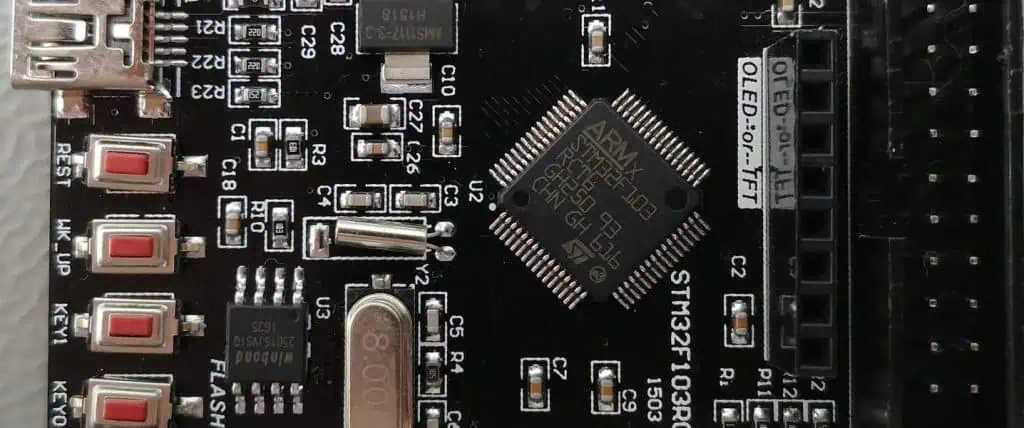
A Gerber file is a standardized vector format used in the electronics industry to describe the layers of a printed circuit board (PCB). It contains information about various PCB elements, including copper traces, solder mask, silkscreen, and drill holes. Essentially, Gerber files serve as a universal language between PCB designers and manufacturers, ensuring that the final product matches the intended design precisely.

A Brief History

The Gerber file format has its roots in the early days of PCB manufacturing. It was developed in the 1960s by Gerber Systems Corporation, founded by H. Joseph Gerber. Initially, these files were used to control vector photoplotters, machines that exposed photoresist-coated materials to light, creating the artwork for PCB production.

Over time, as PCB design became increasingly complex, the Gerber format evolved. The original standard, known as RS-274D, was eventually superseded by the more capable RS-274X format. This newer version, sometimes called “Extended Gerber,” includes additional features that make it more suitable for modern PCB designs.

Industry Standards: RS-274D vs RS-274X

While both RS-274D and RS-274X are referred to as “Gerber” formats, there are significant differences between them:

  1. RS-274D (Standard Gerber):
    • Older format
    • Requires separate aperture definition files
    • Limited in its ability to define complex shapes
  2. RS-274X (Extended Gerber):
    • Modern standard
    • Includes aperture definitions within the file
    • Supports more complex shapes and features
    • More efficient and less prone to errors

Today, RS-274X is the preferred format for most PCB manufacturers due to its enhanced capabilities and reduced potential for misinterpretation.

The Role of Gerber Files in PCB Production

Gerber files play a crucial role in translating PCB designs into physical boards. They act as a set of instructions for manufacturing equipment, guiding processes such as:

  1. Photoplotter imaging
  2. CNC drilling
  3. Solder mask application
  4. Silkscreen printing

By providing precise, layer-by-layer information, Gerber files ensure that every aspect of the PCB design is accurately reproduced during manufacturing. This level of detail is essential for creating functional, high-quality circuit boards that meet the exacting standards of modern electronics.

Read more about:

2. Why Are Gerber Files Important for PCB Manufacturing?

The Cornerstone of PCB Fabrication

Gerber files are the lifeblood of PCB manufacturing. They serve as the primary means of communication between designers and fabricators, ensuring that the final product matches the intended design with utmost precision. Here’s why Gerber files are so crucial:

  1. Universal Language: Gerber files provide a standardized format that can be understood by various manufacturing equipment and software, regardless of the original design tool used.
  2. Layered Information: They contain separate data for each layer of the PCB, allowing manufacturers to create complex, multi-layer boards accurately.
  3. Precision: Gerber files offer high-resolution data, enabling the creation of intricate designs with fine details.

How Manufacturers Use Gerber Files

PCB manufacturers rely on Gerber files to guide every step of the fabrication process. Here’s how different Gerber file layers are used:

  1. Copper Layers: These files guide the etching process to create the conductive traces on the PCB.
  2. Solder Mask Layers: Determine where the protective solder mask should be applied or removed.
  3. Silkscreen Layers: Guide the application of component labels, logos, and other printed information on the board.
  4. Drill Files: While technically not Gerber files (usually in Excellon format), these accompany Gerber files to specify the location and size of holes and vias.

Risks of Incorrect Gerber Files

The importance of accurate Gerber files cannot be overstated. Errors in these files can lead to significant issues:

  1. Production Errors: Inaccurate Gerber files can result in misplaced components, incorrect trace widths, or missing features on the final PCB.
  2. Costly Revisions: Mistakes discovered after production require new boards to be manufactured, leading to increased costs and delays.
  3. Functionality Issues: Errors in Gerber files can create PCBs that fail to function as intended, potentially causing problems in the final product.
  4. Wasted Materials: Incorrect files may lead to scrapped boards, wasting valuable materials and resources.

By understanding the critical role of Gerber files in PCB manufacturing, designers can better appreciate the need for accuracy and attention to detail when preparing these files for production.

3. Components and Layers in a Gerber File

Different software have different method to generate Gerber,EAGLE

Understanding PCB Layers

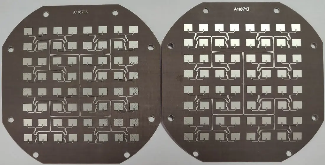
A typical PCB consists of multiple layers, each serving a specific purpose in the board’s functionality. Gerber files provide detailed information for each of these layers, ensuring that the PCB is manufactured exactly as designed. Let’s explore the common layers included in a set of Gerber files:

1. Copper Layers

Copper layers are the heart of any PCB, carrying the electrical signals between components. A typical set of Gerber files includes:

  • Top Copper Layer: Contains the copper traces and pads on the top side of the board.
  • Bottom Copper Layer: Represents the copper traces and pads on the bottom side.
  • Inner Copper Layers: For multi-layer boards, additional copper layers are sandwiched between the top and bottom layers.

2. Solder Mask Layers

Solder mask is a thin lacquer-like layer of polymer that is usually applied to the copper layers of a PCB to protect the copper from oxidation and to prevent solder bridges from forming between closely spaced solder pads. Gerber files for solder mask typically include:

  • Top Solder Mask: Defines areas on the top of the board where solder mask should be applied or removed.
  • Bottom Solder Mask: Specifies solder mask application for the bottom of the board.

3. Silkscreen Layers

Silkscreen layers contain text and symbols printed on the PCB surface, providing valuable information for assembly and future reference. These layers usually include:

  • Top Silkscreen: Text and symbols to be printed on the top side of the board.
  • Bottom Silkscreen: Text and symbols for the bottom side of the board.

4. Drill Files

While not technically Gerber files, drill files are crucial companions to the Gerber set. They specify the location, size, and type of all holes in the PCB. Drill files are typically in Excellon format and include:

  • Plated Holes: For component leads and vias.
  • Non-Plated Holes: For mounting or other mechanical purposes.

5. Board Outline

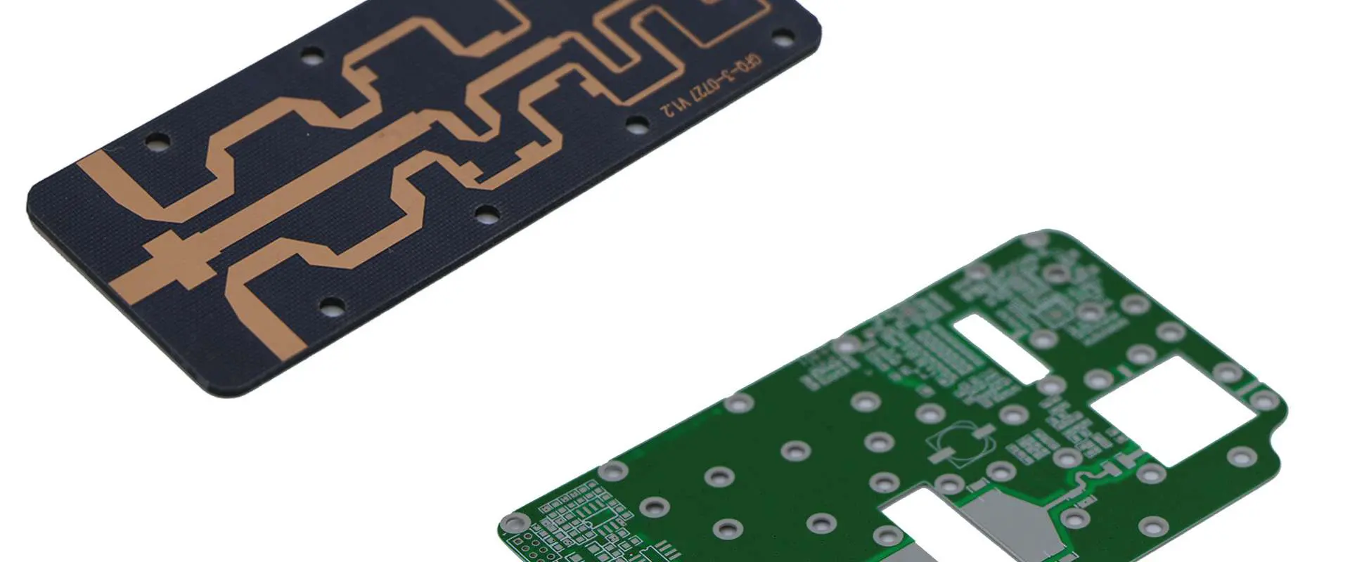
The board outline file defines the physical shape and dimensions of the PCB. It’s crucial for ensuring that the board fits properly into its intended housing or alongside other components.

Example of a Full Set of Gerber Files

A complete set of Gerber files for a typical two-layer PCB might include:

  1. TopCopper.gbr
  2. BottomCopper.gbr
  3. TopSolderMask.gbr
  4. BottomSolderMask.gbr
  5. TopSilkscreen.gbr
  6. BottomSilkscreen.gbr
  7. BoardOutline.gbr
  8. Drill.xln (Excellon drill file)

For more complex multi-layer boards, additional layers would be included, such as Inner1Copper.gbr, Inner2Copper.gbr, etc.

Understanding the components and layers in a Gerber file set is crucial for both PCB designers and manufacturers. It ensures that all necessary information is included and properly organized, leading to accurate and efficient PCB production.

4. How to Generate a Gerber File from PCB Design Software

PCB Design Software Altium Designer

Creating accurate Gerber files is a critical step in the PCB design process. Most modern PCB design software packages include built-in tools for generating Gerber files. While the exact process may vary between different software, the general principles remain the same. Let’s look at how to generate Gerber files using some popular PCB design tools:
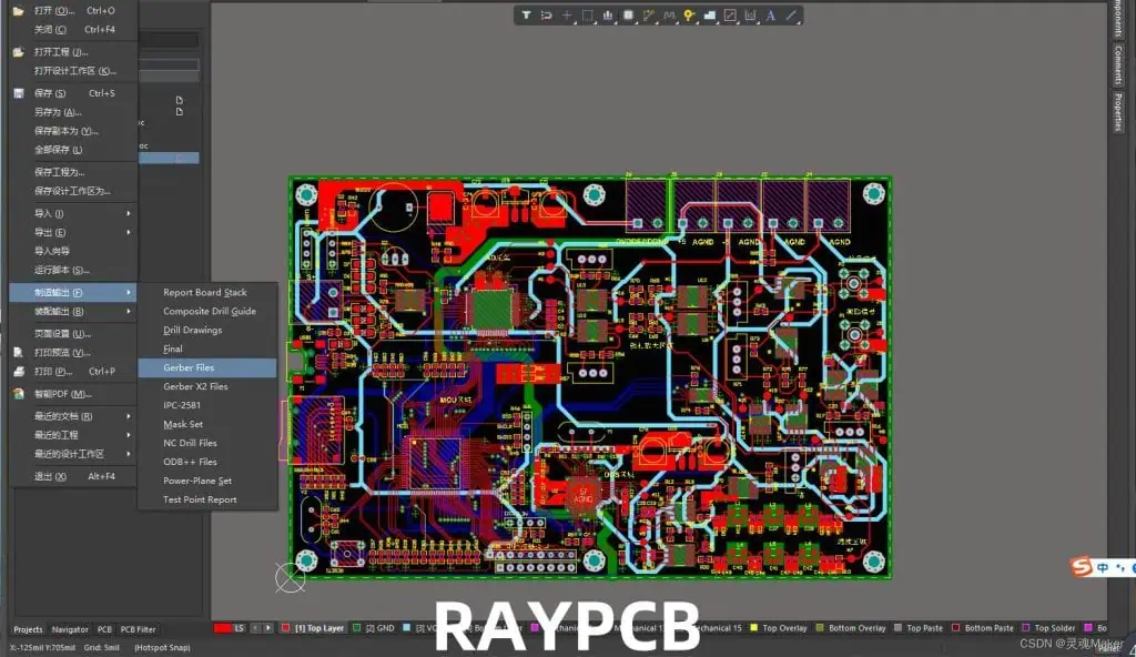
Altium Designer

  1. Open your PCB project in Altium Designer.
  2. Go to “File” > “Fabrication Outputs” > “Gerber Files”.
  3. In the Gerber setup dialog, ensure all necessary layers are selected.
  4. Set the output directory and other parameters as needed.
  5. Click “OK” to generate the Gerber files.

KiCad

  1. Open your PCB layout in KiCad’s PCB Editor.
  2. Go to “File” > “Plot”.
  3. In the Plot dialog, select the layers you want to export.
  4. Choose your output directory and format (typically, use “Gerber” format).
  5. Click “Plot” to generate the files.
  6. For drill files, use the “Generate Drill Files” button in the same dialog.
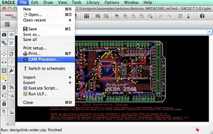
Eagle

  1. Open your board layout in Eagle.
  2. Go to “File” > “CAM Processor”.
  3. In the CAM Processor, select a suitable job file (e.g., “gerb274x.cam” for extended Gerber).
  4. Verify that all necessary layers are included.
  5. Click “Process Job” to generate the Gerber files.

EasyEDA

  1. Open your PCB design in EasyEDA.
  2. Click on the “Fabrication” button in the top toolbar.
  3. In the Fabrication Output dialog, ensure “Gerber” is selected.
  4. Choose your layer setup and other parameters.
  5. Click “Generate Gerber” to create the files.

Common Export Settings to Check

Regardless of the software you’re using, there are several important settings to verify when generating Gerber files:

  1. Units: Ensure the correct unit (inches or millimeters) is selected.
  2. Format: Choose the appropriate Gerber format (typically RS-274X for modern designs).
  3. Layers: Verify that all necessary layers are included in the export.
  4. Precision: Set the coordinate precision (usually 2:4 or 2:5 for inches, 3:3 or 4:4 for millimeters).
  5. Apertures: For older formats, ensure apertures are correctly defined.
  6. Drill File Format: Typically, use Excellon format for drill files.

By carefully checking these settings and following the correct procedures for your specific PCB design software, you can ensure that your Gerber files accurately represent your PCB design and are ready for manufacturing.

5. Best Practices for Preparing and Checking Gerber Files

Preparing and verifying Gerber files is a crucial step in ensuring successful PCB manufacturing. Following best practices can help you avoid costly errors and delays. Here are some key strategies to implement:

Importance of Design Rule Checks (DRC)

Before exporting Gerber files, it’s essential to run a thorough Design Rule Check (DRC) in your PCB design software. DRC helps identify potential issues such as:

  1. Trace width and spacing violations
  2. Clearance errors
  3. Unconnected nets
  4. Drill and pad size mismatches

Resolving these issues before generating Gerber files can prevent many common manufacturing problems.

Using Gerber Viewers for Verification

After generating Gerber files, it’s crucial to verify them using specialized Gerber viewer software. This step allows you to visually inspect your design and catch any issues that might have been missed. Popular Gerber viewers include:

  1. Gerbv: An open-source Gerber viewer for Linux, macOS, and Windows.
  2. ViewMate: A free Gerber viewer from PentaLogix.
  3. GerberLogix: A comprehensive Gerber file viewer and editor.

When using a Gerber viewer:

  1. Load all layers and check their alignment.
  2. Verify that all expected features are present.
  3. Check for any unexpected artifacts or missing elements.
  4. Confirm that drill holes are correctly placed.

Common Mistakes to Avoid

When preparing Gerber files, be aware of these frequent pitfalls:

  1. Missing Layers: Ensure all necessary layers (copper, solder mask, silkscreen, etc.) are included in your Gerber set.
  2. Incorrect Layer Polarity: Verify that positive and negative layers are correctly defined, especially for solder mask and silkscreen.
  3. Mismatched Units: Ensure consistency in units (inches or millimeters) across all files.
  4. Outdated Design Elements: Remove any unused or outdated elements from your design before generating Gerber files.
  5. Incompatible Drill File Format: Make sure your drill file format is compatible with your manufacturer’s requirements.
  6. Inaccurate Board Outline: Verify that the board outline is correctly defined and matches your design intentions.
  7. Insufficient Precision: Use appropriate numerical precision in your Gerber files to ensure accurate representation of your design.

Additional Best Practices

  1. Use Descriptive Filenames: Name your Gerber files clearly and consistently (e.g., ProjectName_TopCopper.gbr).
  2. Include a README File: Provide a text file explaining the contents of your Gerber package, including any special instructions.
  3. Double-Check Drill Files: Ensure that your drill files accurately represent all holes in your design.
  4. Verify Against Manufacturing Guidelines: Check your design against your chosen manufacturer’s specific guidelines and capabilities.
  5. Use Panelization Carefully: If panelizing your design, ensure that the panel layout is correct and includes necessary features like fiducials and breakaway tabs.

By following these best practices and carefully checking your Gerber files before submission, you can significantly reduce the risk of manufacturing errors and ensure a smoother PCB production process.

6. How to Submit Gerber Files to PCB Manufacturers

Submitting Gerber files to PCB manufacturers is the final step in bringing your design to life. Proper submission ensures that your design is interpreted correctly and manufactured efficiently. Here’s a guide to help you through this crucial process:

Zipping and Naming Gerber Files

  1. Create a Zip Archive: Compress all your Gerber files and associated documents into a single ZIP file. This makes it easier to upload and keeps all files together.
  2. Use Clear, Consistent Naming: Name your ZIP file clearly, including the project name and version number (e.g., “ProjectName_v1.0_Gerbers.zip”).
  3. Organize Internal Folders: If your Gerber set is complex, consider organizing files into subfolders within the ZIP (e.g., “Gerbers”, “Drills”, “Documentation”).

Manufacturer-Specific Requirements

Different PCB manufacturers may have specific requirements for Gerber file submissions. Always check with your chosen manufacturer for their particular guidelines. Common requirements include:

  • File Format Versions: Confirm which Gerber format (e.g., RS-274X) and drill file format (e.g., Excellon) the manufacturer prefers.
  • Layer Naming Conventions: Some manufacturers have specific naming conventions for Gerber files (e.g., GTL for top copper, GBL for bottom copper).
  • Additional Documentation: Many manufacturers require a fabrication drawing or assembly drawing along with the Gerber files.
  • Board Specifications: Provide details such as board thickness, copper weight, and material type in a separate document.

Example of a Submission Checklist

To ensure you’ve covered all bases, use a checklist like this when submitting your Gerber files:

  1. Gerber files for all PCB layers (copper, solder mask, silkscreen, etc.)
  2. Drill file (Excellon format)
  3. Board outline file
  4. Fabrication drawing (if required)
  5. Bill of Materials (BOM) for assembly orders
  6. Pick and place file for assembly orders
  7. README file with any special instructions or notes
  8. Confirmation that all files use consistent units (inches or mm)
  9. Verification that file naming follows manufacturer’s conventions
  10. Check that the Gerber format matches manufacturer’s requirements

Tips for a Smooth Submission Process

  1. Use the Manufacturer’s Online Platform: Many PCB manufacturers offer online portals for file submission, which often include automatic design rule checks.
  2. Communicate Special Requirements: If your design has any unusual features or requirements, communicate these clearly to the manufacturer.
  3. Request a Design Review: Some manufacturers offer a design review service. Take advantage of this to catch any potential issues before production.
  4. Keep Versions Organized: If you need to submit revised files, clearly indicate the new version number and what changes were made.
  5. Backup Your Files: Always keep a backup of the submitted Gerber files for your records.

By following these guidelines and maintaining clear communication with your PCB manufacturer, you can significantly increase the chances of a successful and efficient production run.

7. Common Errors and How to Fix Them

Even with careful preparation, errors can occur in Gerber files. Recognizing and addressing these issues promptly can save time and resources. Here are some common Gerber file errors and how to fix them:

1. Misaligned Layers

Problem: Layers in the PCB design do not align correctly when viewed in a Gerber viewer.

Solution:

  • Check the origin point settings in your PCB design software.
  • Ensure all layers use the same coordinate system.
  • Re-export the Gerber files with corrected settings.

2. Missing Apertures

Problem: Certain features are missing or appear incomplete in the Gerber viewer.

Solution:

  • Verify that all necessary apertures are defined in your design.
  • Use the RS-274X format, which includes aperture definitions in the file.
  • Check your PCB design software’s export settings for aperture-related options.

3. Incorrect Board Outline

Problem: The board outline in the Gerber file doesn’t match the intended design.

Solution:

  • Ensure the board outline layer is correctly defined in your PCB design software.
  • Check that the board outline is a closed polygon without any gaps.
  • Verify that the board outline is included in the Gerber export process.

4. Drill File Mismatches

Problem: Drill holes don’t align with pads or are the wrong size.

Solution:

  • Confirm that the drill file uses the same unit and origin as the Gerber files.
  • Check for any scaling issues in the drill file export process.
  • Verify that hole sizes in the design match those in the drill file.

5. Layer Polarity Issues

Problem: Negative layers (like solder mask) appear positive or vice versa.

Solution:

  • Check the layer polarity settings in your PCB design software.
  • Verify that the Gerber file export process correctly handles layer polarities.
  • Use a Gerber viewer to confirm the correct appearance of each layer.

Tips for Troubleshooting

  1. Use Multiple Gerber Viewers: Different viewers may catch different issues.
  2. Compare with Original Design: Open your original PCB design alongside the Gerber files to spot discrepancies.
  3. Check Software Settings: Review your PCB design software’s export settings thoroughly.
  4. Consult with Manufacturers: Many PCB manufacturers offer design for manufacturing (DFM) checks that can catch common errors.
  5. Learn from Mistakes: Keep a log of errors encountered and their solutions for future reference.

By being aware of these common errors and knowing how to address them, you can improve the quality of your Gerber files and reduce the likelihood of manufacturing issues.

8. Future of Gerber Files in PCB Design

PCB Antenna Layout
PCB Antenna Layout

While Gerber files have been the industry standard for decades, the PCB design and manufacturing landscape is constantly evolving. Let’s explore the current trends and potential future of Gerber files in PCB design.

Introduction of New Formats

  1. ODB++: Developed by Mentor Graphics, ODB++ is a comprehensive data format that includes not just PCB layout data, but also component information and manufacturing instructions.
  2. IPC-2581: This open standard, developed by the IPC (Association Connecting Electronics Industries), aims to provide a single, unified data format for PCB manufacturing, assembly, and testing.

Will Gerber Files Still Dominate?

Despite the introduction of these new formats, Gerber files continue to be widely used due to several factors:

  1. Industry Inertia: Many manufacturers and designers are familiar with Gerber files and resistant to change.
  2. Proven Reliability: Gerber files have a long history of successful use in PCB manufacturing.
  3. Continuous Improvements: The Gerber format has evolved over time to meet new requirements, such as the introduction of the X2 format.
  4. Universal Support: Nearly all PCB design software and manufacturing equipment support Gerber files.

However, the limitations of Gerber files, such as the need for multiple files to represent a single board and lack of built-in component information, may gradually lead to increased adoption of newer formats.

Trends in Smart Manufacturing

The future of PCB design and manufacturing is likely to be influenced by broader trends in smart manufacturing:

  1. Increased Automation: More sophisticated data formats may be required to support fully automated manufacturing processes.
  2. Digital Twins: The concept of creating digital representations of physical products may drive the need for more comprehensive data formats.
  3. Industry 4.0: As factories become more connected and data-driven, there may be a push for more integrated design and manufacturing data formats.
  4. AI and Machine Learning: These technologies may be employed to optimize PCB designs and manufacturing processes, potentially requiring more detailed data than traditional Gerber files provide.

While Gerber files are likely to remain important in the near future, PCB designers and manufacturers should stay informed about emerging standards and be prepared to adapt to new technologies and data formats as they gain traction in the industry.

Conclusion

Gerber files remain the cornerstone of PCB design and manufacturing, serving as the critical link between designers’ visions and the physical reality of printed circuit boards. Throughout this guide, we’ve explored the intricacies of Gerber files, from their basic definition to best practices for their creation and use.

We’ve learned that Gerber files are more than just simple design files; they are a universal language in the PCB industry, enabling clear communication between designers and manufacturers. Their importance cannot be overstated, as accurate Gerber files are essential for producing high-quality, functional PCBs.

Key takeaways from this guide include:

  1. The structure and components of Gerber files, including various layers like copper, solder mask, and silkscreen.
  2. Best practices for generating Gerber files from popular PCB design software.
  3. The importance of thorough checking and verification of Gerber files before submission.
  4. Common errors in Gerber files and how to address them.
  5. The future of Gerber files in the context of evolving PCB design and manufacturing technologies.

As we look to the future, it’s clear that while new formats may emerge, Gerber files will continue to play a crucial role in PCB manufacturing for the foreseeable future. However, staying informed about new developments and being prepared to adapt to changing technologies will be crucial for PCB designers and manufacturers alike.

Remember, the key to successful PCB production lies in attention to detail and a thorough understanding of the Gerber file format. By mastering the creation and handling of Gerber files, you can ensure that your PCB designs are accurately translated from digital designs to physical boards, paving the way for innovative and reliable electronic products.

FAQ Section

  1. What is included in a Gerber file? Gerber files typically include data for various PCB layers such as copper traces, solder mask, silkscreen, and board outline. They may also include drill files, though these are often in a separate format like Excellon.
  2. How do I open a Gerber file? Gerber files can be opened using specialized Gerber viewer software. Popular options include Gerbv, ViewMate, and GerberLogix. Many PCB design software packages also include built-in Gerber viewers.
  3. What software creates Gerber files? Most PCB design software can generate Gerber files. This includes popular tools like Altium Designer, KiCad, Eagle, and EasyEDA, among others.
  4. Are Gerber files still used? Yes, Gerber files remain the industry standard for PCB manufacturing. While newer formats like ODB++ and IPC-2581 are gaining traction, Gerber files are still widely used and supported by manufacturers worldwide.
  5. What’s the difference between Gerber and Excellon files? Gerber files typically contain PCB layer information, while Excellon files are specifically used for drill data. Both are usually required for PCB manufacturing, with Excellon files complementing the Gerber set.

After Etch Stress Relief in RT/duroid Microwave Laminates

What are RT/duroid Microwave Laminates?

RT/duroid microwave laminates are special materials used in making high-frequency circuit boards. They’re made by Rogers Corporation and are popular for their excellent properties:

  • Low dielectric constant
  • Low loss tangent
  • Good dimensional stability
  • Effective heat conduction
  • Minimal moisture absorption

These features make them ideal for things like antenna systems, satellite communications, and radar technology.

Powered By EmbedPress

The Etching Process: Where Stress Begins

Etching is a key step in making circuit boards. It removes unwanted copper from the laminate surface to create circuit patterns. However, this process can stress the material in several ways:

  1. Chemical reactions: Etching chemicals can cause localized heating and material changes.
  2. Temperature changes: The process often involves heating and cooling, which can stress the material.
  3. Physical forces: Removing copper can upset the material’s structure.

These stresses aren’t visible right away but can cause problems later.

What is After Etch Stress Relief?

After etch stress relief happens when the stresses from etching slowly release over time. This can happen through:

  1. Viscoelastic relaxation: The material slowly deforms in response to stress.
  2. Temperature cycling: Normal temperature changes cause repeated expansion and contraction.
  3. Moisture absorption: Even small amounts of moisture can cause slight changes.
  4. Copper grain changes: The remaining copper can undergo tiny structural changes.

Read more about:

Why Should We Care About Stress Relief?

Stress relief can cause several issues:

  1. Size changes: The board might slightly shrink or expand.
  2. Warping: The board may not stay flat.
  3. Layer separation: In worst cases, copper layers might peel away from the board.
  4. Tiny cracks: Stress relief can cause small cracks in the material.
  5. Electrical changes: The board’s electrical properties might alter slightly.

These problems can be especially troublesome for high-frequency applications that need precise layouts.

How Can We Reduce Stress Relief Problems?

Here are some strategies to minimize stress relief issues:

  1. Improve etching: Better control of chemicals, temperature, and timing during etching.
  2. Heat treatment: Controlled heating and cooling after etching to relieve stress.
  3. Balanced design: Spread copper more evenly across the board.
  4. Careful handling: Store and handle boards properly to avoid extra stress.
  5. Choose the right material: Some RT/duroid grades handle stress better than others.
  6. Use special finishes: Certain surface treatments can help distribute stress.

Advanced Techniques for Managing Stress

As technology advances, new methods are being developed:

  1. Computer modeling: Using software to predict and minimize stress.
  2. New materials: Scientists are creating materials that resist stress better.
  3. Smart etching machines: Systems that adjust automatically to reduce stress.
  4. Stress-aware design software: Programs that help create layouts with less stress.

Wrapping Up

After etch stress relief is a tricky problem when working with RT/duroid microwave laminates. It’s crucial to understand and manage this issue to make high-quality, reliable circuit boards for demanding applications.

By using the right materials, optimizing manufacturing processes, and employing smart design strategies, we can minimize stress-related problems. As research continues, we’ll likely see even better solutions in the future, allowing us to push the boundaries of high-frequency circuit design even further.

Advances in Integrated Circuit Assembly: Techniques and Innovations

Introduction

In the ever-evolving landscape of modern electronics, integrated circuits (ICs) stand as the cornerstone of technological progress. These miniature marvels, often no larger than a fingernail, are the brains behind our smartphones, computers, and countless other devices that power our digital world. At the heart of bringing these complex components to life lies the crucial process of integrated circuit assembly.

Integrated circuit assembly is the intricate art and science of transforming raw semiconductor materials into functional electronic components. This process involves a series of precise steps, each critical to ensuring the performance, reliability, and longevity of the final product. As technology continues to advance at a breakneck pace, the techniques and innovations in IC assembly play an increasingly vital role in shaping the future of electronics.

YouTube video

This article aims to explore the key techniques, recent innovations, and future trends in integrated circuit assembly. By delving into both traditional methods and cutting-edge advancements, we’ll uncover how this field is pushing the boundaries of what’s possible in electronic design and manufacturing.

Understanding Integrated Circuit Assembly

Definition and Scope

Integrated circuit assembly refers to the process of packaging a semiconductor die (chip) into a functional IC package. This process transforms a bare silicon chip into a protected, usable component that can be integrated into electronic devices. The scope of IC assembly encompasses everything from preparing the die to final testing of the packaged chip.

Overview of Assembly Stages

The integrated circuit assembly process can be broadly divided into four main stages:

  1. Die Preparation: This involves separating individual dies from the processed wafer and preparing them for packaging.
  2. Bonding: The die is attached to the package substrate and electrical connections are made between the die and the package leads.
  3. Packaging: The assembled die is encapsulated in a protective material to shield it from environmental factors and physical damage.
  4. Testing: The packaged IC undergoes rigorous testing to ensure functionality and reliability.

Key Materials Used in IC Assembly

Several crucial materials are employed throughout the IC assembly process:

  • Substrates: Typically made of materials like ceramic, plastic, or glass, these serve as the base for the IC package.
  • Adhesives: Used to attach the die to the substrate.
  • Bonding wires: Usually gold or copper, these create electrical connections between the die and package leads.
  • Encapsulants: Protective materials that surround the die and internal connections.
  • Solder: Used for creating external connections on the package.

Traditional Techniques in IC Assembly

Wire Bonding

Wire bonding is one of the most widely used techniques in IC assembly. It involves creating electrical connections between the die and the package leads using thin wires, typically made of gold or copper.

Types of Wire Bonding

  • Ball bonding
  • Wedge bonding

Advantages

  • Flexible and adaptable to different package types
  • Well-established technology with high reliability
  • Cost-effective for many applications

Flip-Chip Bonding

Flip-chip bonding, also known as controlled collapse chip connection (C4), involves flipping the chip upside down and directly connecting it to the substrate using solder bumps.

Key Features

  • Direct die-to-substrate connection
  • Higher performance due to shorter electrical paths
  • Better heat dissipation

Wafer-Level Packaging

Wafer-level packaging (WLP) is a technique where the IC packaging is done at the wafer level, before the individual chips are separated.

Benefits

  • Smaller package size, approaching chip scale
  • Improved electrical performance
  • Cost-effective for high-volume production

Limitations of Conventional Approaches

While these traditional techniques have served the industry well, they face limitations in meeting the demands of modern electronics:

  • Challenges in achieving extremely fine pitches
  • Thermal management issues in high-performance applications
  • Difficulties in integrating heterogeneous components

Innovations and Emerging Techniques

As the electronics industry pushes for smaller, faster, and more powerful devices, new techniques in integrated circuit assembly have emerged to meet these challenges.

3D Integrated Circuits (3D ICs)

3D ICs represent a significant leap forward in IC assembly, allowing for vertical stacking of multiple dies.

Through-Silicon Vias (TSVs)

TSVs are a key enabling technology for 3D ICs. These are vertical electrical connections that pass through a silicon wafer or die, allowing for direct connections between stacked layers.

Benefits for Performance and Miniaturization

  • Reduced signal delay and power consumption
  • Higher bandwidth between different functional blocks
  • Significant reduction in overall package size

System-in-Package (SiP) Technology

SiP technology takes integration a step further by combining multiple ICs and other components into a single package.

Integration of Heterogeneous Components

SiP allows for the integration of different types of chips and components, such as:

  • Digital and analog ICs
  • Memory chips
  • MEMS devices
  • Passive components

This level of integration enables more compact and powerful electronic systems, crucial for applications like smartphones and IoT devices.

Fan-Out Wafer-Level Packaging (FOWLP)

FOWLP is an advanced wafer-level packaging technique that extends the benefits of WLP to chips with a higher number of I/O connections.

Improved Thermal and Electrical Performance

  • Better heat dissipation due to larger package area
  • Shorter electrical paths leading to improved signal integrity
  • Ability to integrate more I/Os in a smaller form factor

Advanced Materials and Processes

The quest for improved performance has led to the development and adoption of new materials and processes in IC assembly.

Use of Low-k Dielectrics

Low-k dielectric materials are being increasingly used to reduce signal delay and power consumption in high-performance ICs.

New Solder Materials

Lead-free solder alloys and copper pillar bumps are being adopted to meet environmental regulations and improve electrical and thermal performance.

AI-based Inspection Tools

Artificial intelligence and machine learning are being employed in inspection and quality control processes, improving defect detection and yield rates.

Read more about:

Automation and Smart Manufacturing

The integration of advanced automation and smart manufacturing techniques is revolutionizing IC assembly processes.

Role of Robotics and AI in IC Assembly Lines

Robotic systems, guided by sophisticated AI algorithms, are increasingly taking over precision tasks in IC assembly:

  • Die placement and alignment
  • Wire bonding
  • Encapsulation and molding

These systems offer unprecedented levels of accuracy and consistency, crucial for assembling today’s complex ICs.

Quality Control through Machine Learning and Computer Vision

Advanced machine learning algorithms and computer vision systems are being employed to:

  • Detect microscopic defects in real-time
  • Predict potential failures before they occur
  • Optimize process parameters on-the-fly

Benefits: Precision, Yield Improvement, Cost Reduction

The adoption of smart manufacturing techniques in IC assembly offers several key benefits:

  • Improved precision in assembly processes
  • Significant increases in yield rates
  • Reduction in manufacturing costs through increased efficiency and reduced waste

Challenges in Modern Integrated Circuit Assembly

Despite the advancements, the field of IC assembly faces several significant challenges.

Miniaturization and Thermal Management

As ICs continue to shrink while packing in more transistors, two major challenges emerge:

  1. Achieving finer pitches: The need for increasingly fine pitches in interconnects poses significant technical challenges.
  2. Heat dissipation: Smaller packages with higher power densities make thermal management a critical concern.

Cost Pressures and Time-to-Market Demands

The electronics industry’s competitive nature puts immense pressure on manufacturers to:

  • Reduce production costs
  • Shorten development cycles
  • Bring products to market faster

These demands often conflict with the need for reliability and quality, creating a delicate balancing act for IC assembly processes.

Environmental and Regulatory Concerns

The IC assembly industry must navigate an increasingly complex regulatory landscape:

  • RoHS compliance: Ensuring products are free from hazardous substances like lead.
  • Lead-free requirements: Developing and implementing lead-free soldering processes.
  • Sustainability: Addressing the environmental impact of manufacturing processes and materials.

Future Trends in IC Assembly

The future of integrated circuit assembly promises exciting developments and challenges.

Quantum and Neuromorphic Chip Assembly Requirements

As quantum computing and neuromorphic chips move from research to practical applications, they will require novel assembly techniques:

  • Ultra-low temperature packaging for quantum chips
  • High-density, 3D interconnects for neuromorphic systems

Sustainable Assembly Technologies

The push for sustainability is driving research into:

  • Biodegradable packaging materials
  • Energy-efficient assembly processes
  • Improved recycling techniques for electronic components

Integration with Advanced Packaging

The lines between IC assembly and advanced packaging continue to blur, with trends like:

  • Chiplets: Assembling systems from smaller, reusable chip components
  • Interposers: Using silicon or organic interposers for high-density interconnects
  • Embedded die technology: Integrating bare dies directly into PCBs or flexible substrates

Applications Across Industries

The innovations in integrated circuit assembly are enabling advancements across various industries.

Consumer Electronics

In the realm of consumer electronics, advanced IC assembly techniques are enabling:

  • Slimmer, more powerful smartphones
  • Compact and feature-rich wearable devices
  • High-performance gaming consoles and VR headsets

Automotive Electronics

The automotive industry is benefiting from IC assembly innovations in areas such as:

  • Advanced Driver Assistance Systems (ADAS)
  • Electric Vehicle (EV) control systems
  • In-vehicle infotainment and connectivity solutions

Medical Devices and IoT

In healthcare and the Internet of Things, IC assembly advancements are facilitating:

  • Miniaturized implantable medical devices
  • Wearable health monitors with extended battery life
  • Low-power, long-range IoT sensors and devices

Aerospace and Defense

The aerospace and defense sectors leverage cutting-edge IC assembly for:

  • High-reliability avionics systems
  • Advanced radar and communication equipment
  • Radiation-hardened components for space applications

Conclusion

The field of integrated circuit assembly stands at the forefront of technological innovation, continuously pushing the boundaries of what’s possible in electronic design and manufacturing. From traditional wire bonding techniques to cutting-edge 3D IC technologies, the evolution of IC assembly has been nothing short of remarkable.

As we’ve explored in this article, recent innovations like 3D ICs, advanced packaging techniques, and smart manufacturing processes are reshaping the landscape of electronics manufacturing. These advancements are not only meeting the demands for smaller, faster, and more powerful devices but also addressing critical challenges in thermal management, cost reduction, and environmental sustainability.

Looking ahead, the role of integrated circuit assembly in next-generation electronics is set to become even more crucial. As we venture into the realms of quantum computing, neuromorphic systems, and beyond, IC assembly techniques will need to evolve to meet these new challenges. The integration of AI, advanced materials, and sustainable practices will undoubtedly play a significant role in shaping the future of this field.

The journey of innovation in IC assembly is far from over. It calls for continued research, industry collaboration, and a relentless pursuit of technological excellence. As we stand on the brink of new frontiers in electronics, the advancements in integrated circuit assembly will continue to be a driving force, enabling the technologies that will define our future.

Altera Programmer Guide: JTAG Programming for CPLD & FPGA (MAX II, Cyclone IV, EPM240T100C5N) โ€“ Quartus & MAX+II Support & Downloads

1. Introduction to Altera Programmer

In the world of programmable logic devices, the Altera Programmer stands as a crucial tool for engineers and developers working with Complex Programmable Logic Devices (CPLDs) and Field-Programmable Gate Arrays (FPGAs). This comprehensive guide will walk you through the intricacies of using an Altera Programmer, with a focus on JTAG programming for popular devices such as MAX II, Cyclone IV, and the EPM240T100C5N.

What is an Altera Programmer?

An Altera Programmer is a hardware device used to configure Altera (now part of Intel) CPLDs and FPGAs. It serves as the bridge between your development computer and the target device, allowing you to download your designed logic onto the chip.

Key Uses for CPLD and FPGA Devices

CPLDs and FPGAs are versatile semiconductor devices that can be programmed to perform a wide range of digital logic functions. Some key applications include:

  1. Prototyping complex digital systems
  2. Implementing custom interfaces and protocols
  3. Accelerating specific computational tasks
  4. Serving as glue logic in larger electronic systems
YouTube video

Overview of Supported Devices

This guide will focus on programming three popular Altera devices:

  1. MAX II: A family of low-cost, non-volatile CPLDs
  2. Cyclone IV: A series of low-power, high-functionality FPGAs
  3. EPM240T100C5N: A specific MAX II CPLD with 240 macrocells

2. Understanding JTAG Programming

JTAG (Joint Test Action Group) programming is the primary method used for configuring Altera devices. Let’s delve into what JTAG is and why it’s crucial for Altera device programming.

What is JTAG?

JTAG, officially known as IEEE 1149.1 Standard Test Access Port and Boundary-Scan Architecture, is a widely adopted industry standard for testing and programming integrated circuits. It provides a standardized interface for accessing and controlling the pins of a device without direct physical contact.

Why JTAG is Used in Altera Device Programming

JTAG is the preferred method for programming Altera devices due to several advantages:

  1. Standardization: JTAG is an industry-standard protocol, ensuring compatibility across different tools and devices.
  2. In-System Programming: Devices can be programmed while soldered onto a PCB, eliminating the need for specialized sockets.
  3. Daisy-Chaining: Multiple devices can be programmed through a single JTAG interface.
  4. Debugging Capabilities: JTAG allows for real-time debugging and monitoring of device operations.

Comparison of JTAG vs. Other Programming Methods

While JTAG is the primary programming method for Altera devices, it’s worth comparing it to alternative approaches:

  1. JTAG vs. In-Socket Programming:
    • JTAG: In-system programming, no special socket required
    • In-Socket: Requires removing the chip and using a dedicated programmer
  2. JTAG vs. Serial Programming:
    • JTAG: Faster programming speeds, more debugging features
    • Serial: Simpler interface, but limited functionality
  3. JTAG vs. Passive Serial:
    • JTAG: More versatile, supports both programming and debugging
    • Passive Serial: Simpler, but limited to programming only

3. Required Tools & Software

To successfully program Altera devices, you’ll need specific software tools. Let’s explore the essential software required for Altera programming.

Overview of Quartus Prime and MAX+II Programmer

  1. Quartus Prime:
    • Comprehensive development environment for Altera FPGAs and CPLDs
    • Supports device programming, synthesis, place-and-route, and timing analysis
    • Available in different editions: Lite (free), Standard, and Pro
  2. MAX+II Programmer:
    • Legacy tool specifically designed for older MAX series CPLDs
    • Simpler interface focused solely on device programming
    • Still relevant for programming certain MAX II devices

Where to Download Quartus and MAX+II Software

You can download the necessary software from the official Intel FPGA website:

  1. Quartus Prime: https://www.intel.com/content/www/us/en/software/programmable/quartus-prime/overview.html
  2. MAX+II Programmer: https://www.intel.com/content/www/us/en/programmable/downloads/software/max2/max2-index.html

System Requirements and Installation Tips

Before installing Quartus Prime or MAX+II Programmer, ensure your system meets the following requirements:

  1. Operating System:
    • Windows 10/8.1/7 (64-bit versions)
    • Red Hat Enterprise Linux 6 or 7
    • SUSE Enterprise Linux 11 or 12
  2. Processor: Multi-core 64-bit processor (Intel Core i5 or equivalent recommended)
  3. RAM: 8 GB minimum, 16 GB or more recommended
  4. Disk Space: 50 GB minimum for a full installation

Installation Tips:

  1. Download the latest version of Quartus Prime or MAX+II Programmer
  2. Run the installer with administrative privileges
  3. Choose a custom installation path if desired (avoid spaces in the path)
  4. Install device support for your specific Altera devices (MAX II, Cyclone IV)
  5. Restart your computer after installation to ensure all components are properly configured

4. Hardware Setup

Proper hardware setup is crucial for successful Altera device programming. Let’s explore the supported programmers and how to connect them to your target devices.

Supported Altera Programmers

Altera offers several programming hardware options, with the most common being:

  1. USB-Blaster:
    • Original USB-based programmer for Altera devices
    • Widely supported across different software versions
  2. USB-Blaster II:
    • Newer version with improved performance
    • Supports faster programming speeds and additional features

Both programmers are compatible with a wide range of Altera devices, including MAX II, Cyclone IV, and the EPM240T100C5N.

Connecting Your Programmer to MAX II / Cyclone IV Devices

To connect your Altera Programmer to your target device:

  1. Identify the JTAG header on your development board or custom PCB
  2. Connect the 10-pin header of the USB-Blaster or USB-Blaster II to the JTAG pins
  3. Ensure proper orientation (Pin 1 is typically marked on both the cable and board)
  4. Connect the USB end of the programmer to your computer
  5. Power on your target board

Pinout Diagrams and Board Preparation

For successful programming, you need to understand the JTAG pinout:

  1. TCK: Test Clock
  2. TDO: Test Data Out
  3. TDI: Test Data In
  4. TMS: Test Mode Select
  5. nTRST: Test Reset (optional)

Typical 10-pin JTAG header pinout:

 9 7 5 3 1
10 8 6 4 2

1: TCK 2: GND 3: TDO 4: VCC (3.3V) 5: TMS 6: N/C 7: N/C 8: N/C 9: TDI 10: GND

Ensure your board is properly prepared:

  1. Verify power supply connections
  2. Check for any required jumper settings
  3. Confirm that the JTAG pins are not shared with other functions

Read more about:

5. Programming CPLDs and FPGAs

Now that we’ve covered the basics, let’s dive into the step-by-step process of programming Altera devices using JTAG.

Step-by-Step Guide: Programming EPM240T100C5N (MAX II)

  1. Launch Quartus Prime or MAX+II Programmer
  2. Click “Hardware Setup” and select your USB-Blaster
  3. Choose “JTAG” as the programming mode
  4. Click “Add File” and select your .pof file for the EPM240T100C5N
  5. Ensure the “Program/Configure” option is checked
  6. Click “Start” to begin programming
  7. Wait for the operation to complete (indicated by a blue progress bar)
  8. Verify successful programming in the programmer window

Programming Cyclone IV Using Quartus Prime

  1. Open Quartus Prime and your Cyclone IV project
  2. Compile your design to generate a .sof file
  3. Open the Programmer tool (Tools > Programmer)
  4. Select your USB-Blaster in the Hardware Setup
  5. Click “Auto Detect” to identify the JTAG chain
  6. Right-click the detected Cyclone IV device and choose “Change File”
  7. Select your compiled .sof file
  8. Check the “Program/Configure” box
  9. Click “Start” to program the device
  10. Monitor the progress and confirm successful programming

Using .pof and .sof Files with Altera Programmer Tools

Understanding file types is crucial for effective Altera programming:

  1. .sof (SRAM Object File):
    • Used for volatile programming of FPGAs
    • Configuration is lost when power is removed
    • Typically used during development and debugging
  2. .pof (Programmer Object File):
    • Used for non-volatile programming of CPLDs and some FPGAs
    • Configuration is retained after power cycling
    • Used for production programming or when persistent configuration is needed

To convert between file types:

  1. Open Quartus Prime
  2. Go to File > Convert Programming Files
  3. Select the output file type (.pof or .sof)
  4. Add your input file and configure any necessary options
  5. Click “Generate” to create the new file

6. Troubleshooting Common Issues

Even with careful setup, you may encounter issues when programming Altera devices. Here are some common problems and their solutions.

Programmer Not Detected

If your Altera Programmer isn’t recognized:

  1. Check USB connections and try a different port
  2. Reinstall USB-Blaster drivers (found in Quartus installation directory)
  3. Verify the programmer is listed in Device Manager
  4. Try a different USB cable

JTAG Chain Errors

When encountering JTAG chain issues:

  1. Ensure all devices in the chain are powered on
  2. Check JTAG connections for loose or incorrect wiring
  3. Verify the JTAG chain in Quartus (Auto Detect feature)
  4. Try reducing the JTAG clock frequency in the programmer settings

Power Supply and Cable Issues

Power-related problems can cause programming failures:

  1. Verify your board is receiving the correct voltage
  2. Check for any required external power supplies
  3. Ensure the JTAG header is properly connected
  4. Look for any signs of physical damage to cables or connectors

Fixing Quartus-Related Software Problems

Software issues can also hinder programming:

  1. Update Quartus Prime to the latest version
  2. Reinstall device support packages
  3. Clear the Quartus Prime cache (Tools > Options > General > Clear Compilation Database)
  4. Verify project settings match your target device

7. Best Practices for Reliable Programming

To ensure consistent and reliable programming of Altera devices, follow these best practices:

Tips for Consistent JTAG Programming

  1. Use high-quality, short JTAG cables to minimize signal integrity issues
  2. Implement proper power sequencing for your target board
  3. Avoid hot-plugging JTAG connections; always power down before connecting/disconnecting
  4. Use the appropriate programming file type (.sof for volatile, .pof for non-volatile)
  5. Verify device ID and JTAG chain integrity before each programming session

Firmware and Driver Updates

Keeping your software and firmware up-to-date is crucial:

  1. Regularly check for Quartus Prime updates
  2. Update USB-Blaster firmware through Quartus (Tools > Programmer > Hardware Setup)
  3. Ensure your computer’s USB drivers are current
  4. Subscribe to Intel FPGA notifications for critical updates

Verifying Programmed Logic

After programming, always verify your design:

  1. Use the “Verify” option in the programmer tool
  2. Implement a simple test design (e.g., LED blinker) to confirm basic functionality
  3. Utilize Quartus SignalTap II Logic Analyzer for in-depth verification
  4. Perform thorough functional testing of your programmed design

8. Support & Downloads

For additional resources and support, refer to these official Intel/Altera links:

Official Intel/Altera Support Links

  1. Intel FPGA Support Center: https://www.intel.com/content/www/us/en/programmable/support/support-resources.html
  2. Altera Programming Hardware Support: https://www.intel.com/content/www/us/en/programmable/support/support-resources/programming-hardware.html

Download Links for Legacy Tools

  1. MAX+PLUS II Software: https://www.intel.com/content/www/us/en/programmable/downloads/software/max2/max2-index.html
  2. Quartus II Web Edition (13.0sp1): https://www.intel.com/content/www/us/en/programmable/downloads/software/quartus-ii-we/130sp1.html

Documentation and User Manual Links

  1. MAX II Device Handbook: https://www.intel.com/content/www/us/en/programmable/products/cpld/max-series/max-ii/support.html
  2. Cyclone IV Device Handbook: https://www.intel.com/content/www/us/en/programmable/products/fpga/cyclone-series/cyclone-iv/support.html
  3. Quartus Prime Pro Edition User Guide: Programming and Configuration: https://www.intel.com/content/www/us/en/programmable/documentation/ftt1513991830769.html

9. Frequently Asked Questions (FAQs)

How do I install an Altera Programmer driver?

To install the Altera Programmer driver:

  1. Connect the USB-Blaster to your computer
  2. Open Device Manager
  3. Locate the “Altera USB-Blaster” under “Other devices”
  4. Right-click and select “Update Driver Software”
  5. Choose “Browse my computer for driver software”
  6. Navigate to your Quartus installation directory (e.g., C:\altera\quartus\drivers)
  7. Select the appropriate driver folder and click “Next”
  8. Follow the prompts to complete the installation

Which programmer should I use for MAX II devices?

For MAX II devices like the EPM240T100C5N, both the USB-Blaster and USB-Blaster II are suitable. The original USB-Blaster is widely supported across different software versions, while the USB-Blaster II offers improved performance. Choose based on your specific needs and software compatibility.

Can I use Quartus Lite for programming CPLDs?

Yes, Quartus Prime Lite Edition can be used for programming most Altera CPLDs, including MAX II devices like the EPM240T100C5N. However, keep in mind that Quartus Prime Lite may have some limitations compared to the Standard or Pro editions:

  1. Limited device support (but covers most common CPLDs and low-end FPGAs)
  2. Fewer advanced optimization features
  3. Restricted use of some high-end IP cores

For most CPLD programming tasks, Quartus Prime Lite should be sufficient.

10. Conclusion

Mastering the use of an Altera Programmer for JTAG programming of CPLDs and FPGAs is an essential skill for digital design engineers. Throughout this guide, we’ve explored the intricacies of programming devices such as the MAX II, Cyclone IV, and specifically the EPM240T100C5N.

Summary of Programming Workflow

The general workflow for programming Altera devices can be summarized as follows:

  1. Install the necessary software (Quartus Prime or MAX+II Programmer)
  2. Set up your hardware, connecting the Altera Programmer to your target device
  3. Create or open your design project in Quartus Prime
  4. Compile your design to generate programming files (.sof or .pof)
  5. Use the Programmer tool to download the configuration to your device
  6. Verify successful programming and test your design’s functionality

Recommended Programmer Tools

For most Altera device programming tasks, we recommend:

  1. Hardware: USB-Blaster or USB-Blaster II
  2. Software: Quartus Prime (latest version compatible with your device)

These tools provide a robust and flexible platform for programming a wide range of Altera CPLDs and FPGAs.

Encouragement to Explore More Altera Resources

As you continue your journey with Altera programmable logic devices, we encourage you to:

  1. Explore the extensive documentation available on the Intel FPGA website
  2. Participate in online forums and communities dedicated to FPGA development
  3. Experiment with different devices and more complex designs
  4. Stay updated with the latest tools and technologies in the field of programmable logic

By mastering the Altera Programmer and associated tools, you’ve taken a significant step in the world of digital design. The skills you’ve acquired will serve as a strong foundation for tackling more advanced projects and pushing the boundaries of what’s possible with programmable logic.

Remember, the field of FPGAs and CPLDs is constantly evolving, so continue learning and exploring new techniques to stay at the forefront of this exciting technology. Happy programming!

Fabrication Guidelines RT/duroid 5870-5880 High Frequency Circuit Materials (PDF Download)

1. Introduction

RT/duroid 5870 and 5880 are high-frequency circuit materials manufactured by Rogers Corporation. These materials are widely used in the aerospace and defense industries, as well as in commercial high-frequency circuit applications. Their unique properties make them ideal for microwave and RF applications, but they also require specific fabrication guidelines to ensure optimal performance.

Powered By EmbedPress

2. Material Properties

Before diving into the fabrication guidelines, it’s essential to understand the properties of RT/duroid 5870 and 5880:

  • Composition: PTFE (Polytetrafluoroethylene) composite reinforced with glass microfibers
  • Dielectric Constant (ฮตr): 2.33 ยฑ0.02 (5870) and 2.20 ยฑ0.02 (5880)
  • Dissipation Factor: 0.0005 to 0.0012 (10 GHz)
  • Temperature Range: -55ยฐC to +150ยฐC
  • Copper Cladding: Available in various weights (1/4 oz to 2 oz)
  • Thickness: Available in various thicknesses (0.005″ to 0.125″)

These properties contribute to the materials’ excellent electrical and mechanical stability across a wide range of frequencies and environmental conditions.

3. Handling and Storage

3.1. Cleanliness

  • Keep the material clean and free from contamination.
  • Handle with lint-free gloves to prevent oil and dirt transfer.
  • Store in a clean, dry environment.

3.2. Temperature and Humidity

  • Store at room temperature (20-25ยฐC) and moderate humidity (30-60% RH).
  • Avoid extreme temperature fluctuations to prevent warping.

3.3. Packaging

  • Keep materials in their original packaging until ready for use.
  • Use interleaving materials between stacked sheets to prevent scratching.

4. Cutting and Machining

rt duroid 5880
rt duroid 5880

4.1. Cutting Methods

  • Shearing: Use sharp, clean blades and support the material to prevent delamination.
  • Sawing: Use a sharp, fine-toothed saw (carbide-tipped blades recommended).
  • Routing: Use carbide-tipped router bits with high spindle speeds and slow feed rates.

4.2. Drilling

  • Use sharp, clean drill bits (preferably carbide-tipped).
  • Recommended drill speeds: 200-500 rpm for small holes, 50-100 rpm for larger holes.
  • Use a backing material to prevent exit burrs.
  • Clean holes thoroughly after drilling to remove debris.

4.3. Milling

  • Use end mills with 30-45ยฐ helix angles.
  • Recommended spindle speeds: 200-300 sfm (surface feet per minute).
  • Slow feed rates to prevent delamination and ensure clean edges.

5. Copper Etching

5.1. Etching Methods

  • Chemical etching is the preferred method for RT/duroid materials.
  • Common etchants: Ferric Chloride, Ammonium Persulfate, Cupric Chloride.

5.2. Etching Considerations

  • Use fresh etchant solutions for consistent results.
  • Maintain proper temperature and agitation during etching.
  • Rinse thoroughly with deionized water after etching.

5.3. Etch Factor

  • Account for the etch factor when designing circuit features.
  • Typical etch factors: 1.5-2.0 for 1 oz copper, 2.0-2.5 for 2 oz copper.

6. Plating

6.1. Surface Preparation

  • Thoroughly clean and desmear the surface before plating.
  • Use chemical or plasma etching to improve adhesion.

6.2. Plating Methods

  • Electroless copper plating followed by electrolytic copper plating is common.
  • Other finishes (e.g., ENIG, immersion tin) can be applied as needed.

6.3. Plating Considerations

  • Monitor plating bath chemistry and temperature for consistent results.
  • Ensure proper adhesion between the plating and the substrate.

Read more about:

7. Multilayer Fabrication

7.1. Layer Registration

  • Use tooling holes or fiducial marks for accurate layer alignment.
  • Consider using a pinning system for improved registration.

7.2. Bonding

  • Use appropriate bonding films compatible with RT/duroid materials.
  • Follow recommended lamination cycles for temperature, pressure, and time.

7.3. Z-axis Expansion

  • Account for the material’s low Z-axis expansion when designing plated through-holes.
  • Use appropriate via design and plating techniques to ensure reliability.

8. Circuit Patterning

8.1. Photoresist Application

  • Use either dry film or liquid photoresist.
  • Ensure proper adhesion and uniform thickness of the photoresist layer.

8.2. Exposure and Development

  • Use collimated UV light for exposure to achieve sharp feature definition.
  • Develop using recommended chemistry and parameters.

8.3. Fine Line Resolution

  • RT/duroid materials can achieve fine line resolution (down to 2-3 mil lines/spaces).
  • Use appropriate imaging and etching techniques for best results.

9. Surface Finishing

9.1. Solder Mask

  • Use solder masks compatible with high-frequency applications.
  • Apply and cure according to the manufacturer’s recommendations.

9.2. Surface Finishes

  • Common finishes include HASL, ENIG, Immersion Tin, and OSP.
  • Choose a finish compatible with the intended application and assembly process.

10. Assembly Considerations

10.1. Component Attachment

  • Use appropriate soldering techniques (e.g., reflow, wave soldering).
  • Follow recommended temperature profiles to avoid damaging the substrate.

10.2. Thermal Management

11. Testing and Quality Control

11.1. Electrical Testing

  • Perform impedance testing to ensure proper transmission line characteristics.
  • Use time-domain reflectometry (TDR) for high-frequency circuit verification.

11.2. Mechanical Testing

  • Check for proper layer adhesion in multilayer constructions.
  • Perform peel strength tests on copper foil as needed.

11.3. Environmental Testing

  • Conduct thermal cycling tests to verify thermal stability.
  • Perform humidity and salt spray tests for applications requiring environmental resistance.

12. Safety Considerations

12.1. Material Handling

  • Use appropriate personal protective equipment (PPE) when handling and fabricating RT/duroid materials.
  • Follow proper ventilation guidelines, especially during machining or high-temperature processes.

12.2. Chemical Safety

  • Handle etchants, plating solutions, and other chemicals according to safety data sheets (SDS).
  • Dispose of chemicals and waste materials in accordance with local regulations.

13. Conclusion

Fabricating high-frequency circuits using RT/duroid 5870 and 5880 materials requires attention to detail and adherence to specific guidelines. By following these fabrication best practices, manufacturers can ensure optimal performance and reliability of their high-frequency circuits. Always consult the latest technical data sheets and processing guides provided by Rogers Corporation for the most up-to-date information and recommendations.

STM32 PCB Design Guide โ€“ From Blue Pill to Custom Boards (STM32F103C8T6)

I. Introduction

The world of embedded systems has been revolutionized by the STM32 family of microcontrollers, offering a perfect blend of performance, versatility, and cost-effectiveness. At the heart of many projects lies the STM32 PCB, a custom-designed circuit board that brings these powerful microcontrollers to life in specific applications.

This STM32 PCB guide will walk you through designing your own custom board, starting from the popular Blue Pill development board to a full production-ready layout. Whether you’re a hobbyist looking to create your next IoT gadget or a professional engineer developing a new product, understanding the intricacies of STM32 PCB design is crucial for success in the embedded world.

YouTube video

The STM32 family, developed by STMicroelectronics, encompasses a wide range of 32-bit ARM Cortex-M based microcontrollers. Among these, the STM32F103C8T6, commonly known as the “Blue Pill,” has gained immense popularity due to its affordability and impressive feature set. This guide will focus on this particular model, but the principles discussed can be applied to other STM32 variants as well.

II. Why Choose STM32 for Custom PCB Designs?

The STM32 family of microcontrollers has become a go-to choice for many embedded developers, and for good reason. Let’s explore the benefits that make STM32, particularly the STM32F103C8T6, an excellent choice for custom PCB designs.

Performance and Features

STM32 microcontrollers offer exceptional performance:

  • High-speed operation (72 MHz for the STM32F103C8T6)
  • Advanced peripherals (timers, ADCs, communication interfaces)
  • DMA controllers for efficient data transfer
  • Low power consumption modes

Cost-Effectiveness

Despite their advanced features, STM32 microcontrollers are remarkably affordable:

  • Low unit cost, especially in bulk quantities
  • Reduced overall BOM cost due to integrated peripherals
  • Availability of low-cost development tools

Ecosystem and Support

STM32 benefits from a robust ecosystem:

  • Comprehensive development tools (STM32CubeIDE, STM32CubeMX)
  • Extensive documentation and application notes
  • Active community support and third-party libraries

Popularity of STM32F103C8T6 (“Blue Pill”)

The STM32F103C8T6, nicknamed “Blue Pill,” has gained cult status among hobbyists and professionals alike:

  • Affordable and widely available
  • Compact form factor with breadboard-friendly pinout
  • Sufficient resources for a wide range of projects
  • Large community and abundance of online resources

Use Cases

STM32 microcontrollers, including the Blue Pill, find applications in various domains:

  1. Robotics:
    • Motor control and sensor integration
    • Real-time processing for navigation and obstacle avoidance
  2. Internet of Things (IoT):
    • Low-power wireless sensor nodes
    • Smart home devices and wearables
  3. Industrial Control:
    • PLC replacements and smart actuators
    • Data acquisition and processing systems
  4. Consumer Electronics:
    • Audio processing devices
    • User interface controllers for appliances
  5. Automotive:
    • In-vehicle infotainment systems
    • Sensor fusion for ADAS (Advanced Driver Assistance Systems)

The versatility and performance of STM32 microcontrollers make them suitable for a wide range of applications, from simple hobby projects to complex industrial systems.

Read more about:

III. Understanding the Blue Pill Board (STM32F103C8T6)

Before diving into custom STM32 PCB design, it’s essential to understand the Blue Pill board, which serves as an excellent starting point for many projects.

Pinout and Core Components

The Blue Pill board is built around the STM32F103C8T6 microcontroller and includes several key components:

  1. STM32F103C8T6 MCU:
    • 72 MHz ARM Cortex-M3 core
    • 64 KB Flash memory, 20 KB SRAM
    • Various peripherals (USART, SPI, I2C, USB, CAN, etc.)
  2. Power Supply:
    • 3.3V regulator for the MCU
    • 5V input via USB or external source
  3. Crystal Oscillators:
    • 8 MHz main oscillator
    • 32.768 kHz RTC oscillator (not populated by default)
  4. User Interfaces:
    • User LED (PC13)
    • BOOT0 and RESET buttons
  5. Programming Interfaces:
    • SWD header for debugging
    • USB for power and communication
  6. I/O Headers:
    • All MCU pins broken out to headers

Limitations of Off-the-Shelf Boards

While the Blue Pill is an excellent prototyping platform, it has limitations for production use:

  1. Form Factor:
    • Fixed size and shape may not fit all project enclosures
  2. Component Selection:
    • Limited to pre-selected components, which may not be optimal for all applications
  3. Power Efficiency:
    • Generic design may not be optimized for low-power applications
  4. Peripheral Access:
    • Not all MCU features may be easily accessible
  5. Customization:
    • Limited ability to add project-specific components or interfaces

When to Move to a Custom STM32 PCB

Consider designing a custom STM32 PCB when:

  1. You need a specific form factor or size constraint
  2. Your project requires additional components or interfaces not present on the Blue Pill
  3. You aim to optimize power consumption for battery-operated devices
  4. You want to reduce production costs for medium to large-scale manufacturing
  5. Your application needs enhanced reliability or specific certifications
  6. You’re developing a commercial product and need full control over the design

Moving to a custom STM32 PCB allows you to tailor the design to your specific needs, optimize performance, and potentially reduce costs in production scenarios.

IV. Step 1: Define Your STM32 Project Requirements

Before embarking on your STM32 PCB design journey, it’s crucial to clearly define your project requirements. This step will guide your decisions throughout the design process and help ensure your final PCB meets all necessary specifications.

Choosing the Right STM32 MCU Variant

While this guide focuses on the STM32F103C8T6, there are numerous STM32 variants to choose from:

  1. Performance requirements:
    • Clock speed (from 48 MHz to 480 MHz)
    • Memory size (Flash and RAM)
    • FPU (Floating Point Unit) presence
  2. Peripherals needed:
    • Number and type of communication interfaces
    • ADC resolution and sampling rate
    • Timer functionality
  3. Power consumption:
    • Low-power modes available
    • Sleep current
  4. Package type and size:
    • LQFP, BGA, or other package options
    • Pin count (from 32 to 200+ pins)

Use STM32CubeMX or ST’s product selector tool to find the best match for your project.

Peripheral Needs

List all the peripherals your project requires:

  1. Communication interfaces:
    • UART for serial communication
    • I2C for sensor integration
    • SPI for high-speed data transfer
    • USB for PC connectivity or power
    • CAN for industrial applications
  2. Analog interfaces:
    • ADC for sensor readings
    • DAC for signal generation
  3. Timing and control:
    • PWM for motor control or LED dimming
    • General-purpose timers
  4. External memory interface:
    • FSMC for connecting external RAM or Flash
  5. Debug interface:
    • SWD for programming and debugging

Power Supply and Voltage Regulation

Consider your power supply requirements:

  1. Input voltage range:
    • Battery-powered or mains-powered?
    • USB power option?
  2. Voltage regulation:
    • Linear regulators for low noise
    • Switching regulators for high efficiency
  3. Multiple voltage domains:
    • 3.3V for the MCU core
    • 5V or 12V for peripheral components
  4. Power consumption:
    • Estimated current draw
    • Need for low-power modes

Size, Enclosure, and I/O Considerations

Factor in physical constraints:

  1. PCB dimensions:
    • Maximum size allowed by the enclosure
    • Multi-board design for complex systems
  2. Enclosure requirements:
    • Environmental protection (IP rating)
    • Heat dissipation needs
  3. I/O access:
    • Connectors for external interfaces
    • Test points for debugging
  4. User interface elements:
    • LEDs for status indication
    • Buttons or switches for user input
  5. Mounting considerations:
    • Screw holes or standoffs
    • Edge connectors for modular designs

By thoroughly defining these requirements, you set a solid foundation for your STM32 PCB design, ensuring that the final product will meet all necessary specifications and perform optimally in its intended application.

V. Step 2: STM32 Schematic Design

With your project requirements clearly defined, the next step is to create the schematic for your custom STM32 PCB. The schematic is a detailed diagram that represents all the electrical connections in your circuit.

Using EDA Tools

Several Electronic Design Automation (EDA) tools are popular for STM32 PCB design:

  1. KiCad:
    • Open-source and free
    • Powerful features and growing community support
  2. Eagle:
    • Popular among hobbyists and small businesses
    • Extensive component libraries
  3. Altium Designer:
    • Professional-grade tool with advanced features
    • Excellent for complex, multi-layer designs

Choose a tool that matches your skill level and project complexity. Many offer free versions or trials, allowing you to experiment before committing.

Essential Parts of the STM32 Circuit

STM32F103C8T6 Wiring

  1. Power pins:
    • Connect VDD pins to 3.3V
    • Connect VSS pins to ground
    • Add decoupling capacitors (0.1ฮผF) close to each VDD pin
  2. Boot mode selection:
    • BOOT0 pin with pull-down resistor
    • BOOT1 pin (PB2) with pull-down resistor
  3. Reset circuit:
    • NRST pin with pull-up resistor and capacitor to ground
    • Optional reset button
  4. Clock sources:
    • HSE: 8 MHz crystal with load capacitors
    • LSE: 32.768 kHz crystal for RTC (optional)

Power Supply

  1. Voltage regulator:
    • LDO for 3.3V from 5V input
    • Consider adding a 5V regulator if using higher input voltages
  2. Bypass capacitors:
    • 10ฮผF to 100ฮผF electrolytic or tantalum near voltage regulators
    • 0.1ฮผF ceramic capacitors near ICs

Reset Circuit

  1. Reset button:
    • Momentary switch between NRST and ground
    • Series resistor (470ฮฉ) to limit current
  2. Power-on reset:
    • RC circuit with 10kฮฉ resistor and 0.1ฮผF capacitor

External Crystal Oscillator

  1. 8 MHz crystal:
    • Connected between OSC_IN (PD0) and OSC_OUT (PD1)
    • Two load capacitors (typically 20pF) to ground
  2. Optional 32.768 kHz crystal for RTC:
    • Connected between PC14 and PC15
    • Two load capacitors (typically 12pF) to ground

Programming Header

  1. SWD interface:
    • SWDIO (PA13) and SWCLK (PA14) pins
    • 2×5 pin header for ST-Link compatibility
  2. UART bootloader (optional):
    • USART1 TX (PA9) and RX (PA10) pins
    • Consider adding a USB-to-UART bridge chip

Best Practices in STM32 Schematic Design

  1. Use clear and consistent naming conventions for components and nets.
  2. Group related components together for better readability.
  3. Add detailed notes and comments to explain non-obvious design choices.
  4. Include test points for important signals to aid in debugging.
  5. Consider adding protection components like TVS diodes for exposed I/O.
  6. Use hierarchical sheets for complex designs to improve organization.
  7. Perform thorough Electrical Rule Checks (ERC) to catch common errors.

By following these guidelines and paying attention to detail in your schematic design, you’ll create a solid foundation for the PCB layout phase of your STM32 project.

VI. Step 3: STM32 PCB Layout Best Practices

Once your schematic is complete and error-free, it’s time to move on to the PCB layout. This stage transforms your circuit diagram into a physical board design, considering factors like component placement, trace routing, and signal integrity.

Component Placement Strategy

Effective component placement is crucial for a successful STM32 PCB design:

  1. Place the STM32 microcontroller centrally:
    • This allows for easier routing to peripherals and connectors.
  2. Group related components:
    • Keep decoupling capacitors close to their respective ICs.
    • Place crystal oscillators near the MCU’s oscillator pins.
  3. Consider thermal management:
    • Keep heat-generating components (e.g., voltage regulators) away from sensitive parts.
  4. Optimize for signal integrity:
    • Minimize trace lengths for high-speed signals.
    • Keep analog and digital sections separated.
  5. Plan for assembly and testing:
    • Align components in a way that simplifies the manufacturing process.
    • Leave space for test points near critical signals.

Power and Ground Plane Layout

Proper power distribution is essential for reliable STM32 PCB operation:

  1. Use solid ground planes:
    • Dedicate at least one layer to a continuous ground plane.
    • For multi-layer boards, consider using multiple ground planes.
  2. Implement star grounding:
    • Connect sensitive analog grounds to a single point on the main ground plane.
  3. Use wide traces or copper pours for power distribution:
    • Minimize voltage drop across the board.
    • Consider using polygons for main power nets.
  4. Separate analog and digital power:
    • Use separate power planes or traces for analog and digital supplies.
    • Connect these at a single point near the power source.

Trace Width, Spacing, and Signal Routing

Follow these guidelines for optimal signal routing:

  1. Calculate appropriate trace widths:
    • Use wider traces for power and high-current signals.
    • Standard signal traces can be 6-10 mil wide.
  2. Maintain consistent trace spacing:
    • Typically 6-10 mil for standard signals.
    • Increase spacing for high-voltage or noisy signals.
  3. Use 45-degree angles for trace corners:
    • Avoid 90-degree bends to reduce reflections.
  4. Keep high-speed traces short and direct:
    • Minimize length and avoid unnecessary vias for critical signals.
  5. Use differential pair routing for high-speed interfaces:
    • Maintain equal length and consistent spacing between pairs.

Guidelines for USB, ADC, and High-Speed I/O Traces

  1. USB routing:
    • Keep D+ and D- traces close and matched in length.
    • Maintain 90ฮฉ differential impedance.
    • Avoid vias if possible; if necessary, use them in pairs.
  2. ADC considerations:
    • Keep analog traces short and away from digital signals.
    • Use a ground guard ring around sensitive analog components.
    • Consider using a split ground plane for analog and digital sections.
  3. High-speed I/O:
    • Route clock lines first, then other high-speed signals.
    • Use length matching for parallel buses.
    • Consider using microstrip or stripline techniques for controlled impedance.

EMI/EMC Considerations in STM32 PCB Layout

  1. Keep loop areas small for high-frequency signals.
  2. Use ground planes to provide low-impedance return paths.
  3. Consider adding ferrite beads on power lines to suppress high-frequency noise.
  4. Use shielding techniques for sensitive analog circuits or in noisy environments.
  5. Implement proper grounding for connectors and I/O ports.

Two-Layer vs. Four-Layer Design Decisions

When designing your STM32 PCB, you’ll need to choose between a two-layer or four-layer board:

Two-Layer PCBs:

  • Pros: Lower cost, simpler manufacturing process.
  • Cons: More challenging routing, potential signal integrity issues.
  • Best for: Simple designs, low-speed applications, cost-sensitive projects.

Four-Layer PCBs:

  • Pros: Better signal integrity, easier routing, dedicated power/ground planes.
  • Cons: Higher cost, more complex manufacturing.
  • Best for: Complex designs, high-speed signals, professional products.

For most STM32 projects, a four-layer board offers the best balance of performance and design flexibility. A typical four-layer stackup might include:

  1. Top layer: Components and signal routing
  2. Inner layer 1: Ground plane
  3. Inner layer 2: Power plane
  4. Bottom layer: Components and signal routing

This configuration provides excellent signal integrity and simplifies power distribution.

VII. Step 4: Prototyping and Fabrication

After completing your PCB layout, the next exciting phase is bringing your design to life through prototyping and fabrication.

Generating Gerber Files and BOM

  1. Gerber file generation:
    • Use your EDA tool to export Gerber files, which contain all the necessary information for PCB fabrication.
    • Include files for all copper layers, solder mask, silkscreen, and drill holes.
    • Double-check that all layers are correctly aligned and scaled.
  2. Creating a Bill of Materials (BOM):
    • List all components, including their values, packages, and quantities.
    • Include manufacturer part numbers and potential alternative parts.
    • Organize the BOM in a clear, spreadsheet format for easy reference.

PCB Prototyping Services

For prototype runs or small batches, consider these popular PCB fabrication services:

  1. JLCPCB:
    • Known for fast turnaround and low costs.
    • Offers PCB assembly services as well.
  2. PCBWay:
    • Wide range of PCB manufacturing options.
    • Good for both prototypes and small production runs.
  3. OSH Park:
    • Specializes in high-quality, small-batch PCBs.
    • Purple solder mask is their signature look.

When selecting a service, consider:

  • Minimum order quantity
  • Turnaround time
  • Board specifications (layer count, minimum trace width, etc.)
  • Quality and reliability
  • Additional services like stencil manufacturing or assembly

Assembly: Manual Soldering vs. Reflow Oven

Decide between manual soldering and reflow soldering based on your design complexity and component types:

Manual Soldering:

  • Suitable for through-hole components and simple designs.
  • Requires patience and steady hands.
  • Use a temperature-controlled soldering iron and appropriate flux.

Reflow Soldering:

  • Better for designs with many surface-mount components.
  • Requires a reflow oven or hot air station.
  • Steps include:
    1. Applying solder paste using a stencil
    2. Placing components with tweezers or a pick-and-place machine
    3. Carefully controlling temperature profile in the reflow oven

For many STM32 projects, a combination of both methods might be necessary.

Testing the Custom STM32 Board

Once assembled, it’s crucial to thoroughly test your custom STM32 PCB:

  1. Visual inspection:
    • Check for solder bridges, missing components, or obvious defects.
  2. Continuity testing:
    • Use a multimeter to verify connections and check for shorts.
  3. Power-up test:
    • Use a current-limited power supply for initial power-up.
    • Monitor power consumption and check voltage levels at key points.
  4. Functional testing:
    • Upload a simple test firmware (e.g., blinking LED).
    • Verify basic functionality of all major subsystems.
  5. Comprehensive testing:
    • Test all peripherals and interfaces.
    • Perform stress tests under various operating conditions.

VIII. Step 5: Programming and Debugging STM32 PCBs

With your custom STM32 PCB assembled and basic functionality verified, it’s time to dive into programming and debugging your board.

Uploading Firmware to STM32

There are two primary methods for uploading firmware to your STM32 board:

1. SWD with ST-Link V2

Serial Wire Debug (SWD) is the most common method for programming and debugging STM32 microcontrollers:

  • Connect ST-Link V2 programmer to your board’s SWD header.
  • Use STM32CubeIDE or OpenOCD to upload firmware.
  • Allows for real-time debugging and breakpoints.

2. UART Bootloader with USB-to-Serial Adapter

For boards without an SWD header or for field updates:

  • Activate bootloader mode (usually by setting BOOT0 pin high).
  • Connect a USB-to-Serial adapter to the UART pins.
  • Use STM32CubeProgrammer or other flashing tools to upload firmware.

Tools for STM32 Development

  1. STM32CubeIDE:
    • Integrated Development Environment for STM32 programming.
    • Includes debugging capabilities and peripheral configuration tools.
  2. STM32CubeMX:
    • Graphical tool for STM32 microcontroller configuration.
    • Generates initialization code based on your configuration.
  3. OpenOCD:
    • Open-source debugging tool, useful for command-line enthusiasts.
    • Can be integrated with GDB for advanced debugging.

Basic Firmware Setup for Testing I/O

To verify your custom STM32 PCB’s functionality, start with a simple firmware test:

  1. LED blink test:
    • Configure a GPIO pin as output.
    • Toggle the pin state in a loop with a delay.
  2. Button input test:
    • Configure a GPIO pin as input with pull-up.
    • Read the pin state and toggle an LED based on button press.
  3. UART communication test:
    • Initialize UART peripheral.
    • Implement a simple echo program or periodic message transmission.

These basic tests help verify core functionality before moving on to more complex applications.

IX. Design Tips for Reliable STM32 PCBs

To ensure your custom STM32 PCB performs reliably in real-world conditions, consider these advanced design tips:

Decoupling Capacitor Placement

Proper decoupling is crucial for stable operation:

  • Place 0.1ฮผF ceramic capacitors as close as possible to each VDD pin.
  • Use larger capacitors (1-10ฮผF) near voltage regulators.
  • Consider using ferrite beads in series with power lines for additional filtering.

Reset and Boot Mode Management

Ensure reliable startup and programming:

  • Implement proper reset circuitry with a pull-up resistor and capacitor.
  • Use jumpers or DIP switches for BOOT0/BOOT1 selection if needed.
  • Consider adding an external watchdog timer for enhanced reliability.

Over-Voltage and ESD Protection

Protect your STM32 from electrical hazards:

  • Use TVS diodes on exposed I/O pins.
  • Implement reverse polarity protection on power inputs.
  • Consider adding ESD protection devices on communication interfaces.

Design for Manufacturability and Testability

Optimize your design for production and quality assurance:

  • Use standard component sizes and packages when possible.
  • Include test points for critical signals.
  • Consider adding a PCB version number and date code.
  • Design for automated optical inspection (AOI) by ensuring adequate clearance around components.

X. Real-World Applications of STM32 Custom Boards

Custom STM32 PCBs find applications in various fields:

Wearables

  • Fitness trackers with integrated sensors
  • Smart watches with custom displays
  • Health monitoring devices

Smart Sensors

  • IoT-enabled environmental monitors
  • Industrial process control sensors
  • Smart home automation devices

Drones and Robotics

  • Flight controllers for quadcopters
  • Motor control boards for robotic arms
  • Navigation systems for autonomous vehicles

DIY and Maker Projects

  • Custom game consoles
  • Audio processing devices
  • Open-source scientific instruments

These examples demonstrate the versatility of STM32 microcontrollers and the potential of custom PCB designs in bringing innovative ideas to life.

XI. Resources and Tools

To further your STM32 PCB design skills, explore these resources:

STM32CubeMX and STM32CubeIDE

  • Official ST tools for STM32 configuration and development
  • Extensive documentation and tutorials available on ST’s website

Reference Schematics and PCB Layouts

  • ST’s Nucleo and Discovery board designs
  • Open-source projects on platforms like GitHub

STM32 Datasheets and Application Notes

  • Detailed technical information on STM32 microcontrollers
  • Best practices and design guidelines from ST

Online Communities and Forums

  • STM32Duino: Community-driven Arduino-like environment for STM32
  • ST Community: Official forum for STM32 developers
  • Reddit r/embedded: Discussions on embedded systems, including STM32

XII. Conclusion

The journey from the Blue Pill to a fully customized STM32 PCB is both challenging and rewarding. By mastering the art of STM32 PCB design, you open the door to creating highly optimized, application-specific embedded systems.

Whether you’re upgrading from the Blue Pill or building a product, mastering STM32 PCB design opens the door to professional embedded development. The skills you’ve gained in schematic design, PCB layout, and prototyping are invaluable in today’s technology-driven world.

Remember that PCB design is both an art and a science. While following best practices is important, there’s also room for creativity and innovation. Each project brings new challenges and opportunities for learning.

We encourage you to start designing your own STM32 boards. Begin with simple designs, gradually tackling more complex challenges. Experiment with different peripherals, explore various STM32 variants, and push the boundaries of what’s possible within the constraints of PCB design.

The field of embedded systems is ever-evolving, with STM32 at the forefront of many innovations. Stay curious, keep learning, and don’t hesitate to engage with the vibrant community of makers, engineers, and hobbyists who share your passion for STM32 PCB design.

Your next custom STM32 PCB could be the foundation of a groundbreaking product or the solution to a complex problem. So fire up your favorite EDA tool, choose an STM32 microcontroller, and start designing. The world of custom STM32 PCBs awaits your creativity and expertise!

XIII. FAQ

To address common queries and enhance SEO, here are answers to frequently asked questions about STM32 PCB design:

What is the STM32F103C8T6 Blue Pill?

The STM32F103C8T6 Blue Pill is a popular, low-cost development board featuring the STM32F103C8T6 microcontroller. It’s known for its compact size, breadboard-friendly design, and extensive GPIO options, making it a favorite among hobbyists and prototypers for STM32-based projects.

How do I design a custom STM32 PCB?

Designing a custom STM32 PCB involves several steps:

  1. Define your project requirements and choose an appropriate STM32 microcontroller.
  2. Create a schematic diagram using EDA software.
  3. Develop the PCB layout, carefully placing components and routing traces.
  4. Generate manufacturing files (Gerbers) and order a prototype.
  5. Assemble and test your PCB, making iterations as necessary.

Which software is best for STM32 PCB layout?

Popular software options for STM32 PCB layout include:

  • KiCad: Free, open-source, and feature-rich.
  • Altium Designer: Professional-grade with advanced features.
  • Eagle: User-friendly with a large component library.
  • Fusion 360 Electronics: Integrates electrical and mechanical design.

Choose software that aligns with your project complexity and budget.

Can I use STM32CubeMX for PCB design?

STM32CubeMX is primarily a microcontroller configuration and code generation tool, not a PCB design software. However, it can be extremely useful in the early stages of PCB design:

  • It helps in pin assignment and peripheral configuration.
  • It can generate a partial schematic of the microcontroller connections.
  • The configuration can be exported to PCB design tools for further development.

For actual PCB layout, you’ll need to use dedicated EDA software.

How do I program a custom STM32 board?

Programming a custom STM32 board can be done in several ways:

  1. Using SWD (Serial Wire Debug) with an ST-Link programmer:
    • Connect the ST-Link to your board’s SWD pins.
    • Use STM32CubeIDE or OpenOCD to upload firmware.
  2. Using the UART bootloader:
    • Set the BOOT0 pin high to enter bootloader mode.
    • Use a USB-to-UART adapter and STM32CubeProgrammer to upload firmware.
  3. Using a custom bootloader:
    • Implement a bootloader that allows firmware updates over various interfaces (USB, CAN, Ethernet, etc.).

The method you choose depends on your board design and project requirements.

CoolRunner-II CPLD Guide: Features, Applications, and Development Board Setup

Introduction

In the ever-evolving world of digital electronics, programmable logic devices (PLDs) have revolutionized the way engineers design and implement complex digital systems. Among these versatile devices, the CoolRunner-II CPLD family by Xilinx stands out as a popular choice for many applications. This guide will explore the features, applications, and setup process of the CoolRunner-II CPLD, with a focus on the widely used XC2C64A model.

The CoolRunner-II CPLD, also known as CoolRunner II or CoolRunner 2, continues to be a go-to solution for designers seeking low-power, high-performance programmable logic. Its enduring popularity stems from its unique combination of ultra-low power consumption, instant-on capability, and versatile features that make it ideal for a wide range of applications.

In this comprehensive guide, we’ll delve into the key features of the CoolRunner-II CPLD, explore its typical applications, and provide a step-by-step tutorial for setting up and using the CoolRunner-II CPLD starter board and development board. Whether you’re a seasoned engineer or a newcomer to the world of programmable logic, this guide will equip you with the knowledge to harness the power of the CoolRunner-II CPLD in your projects.

YouTube video

1. What is the CoolRunner-II CPLD?

Definition of a CPLD

A Complex Programmable Logic Device (CPLD) is a type of programmable logic device that allows designers to implement custom digital circuits. CPLDs consist of a set of logic blocks connected by a programmable interconnect matrix, enabling the creation of complex digital systems on a single chip.

Brief History of the Xilinx CoolRunner-II CPLD Family

The CoolRunner-II CPLD family was introduced by Xilinx in the early 2000s as a successor to the original CoolRunner series. It was designed to meet the growing demand for low-power, high-performance programmable logic in portable and battery-operated devices.

Differences Between CoolRunner II and Earlier Generations

CoolRunner-II CPLDs offer several improvements over their predecessors:

  1. Lower power consumption
  2. Higher operating speeds
  3. Increased logic density
  4. Enhanced I/O capabilities
  5. Improved design software support

Key Models

The CoolRunner-II CPLD family includes several models, with the XC2C64A being one of the most popular. Other models in the series include:

  • XC2C32A
  • XC2C128
  • XC2C256
  • XC2C384
  • XC2C512

Each model offers different numbers of macrocells and I/O pins, allowing designers to choose the most appropriate device for their specific requirements.

Read more about:

2. Key Features of CoolRunner-II CPLDs

xilinx-spartan-6-fpga-tutorial

Ultra-Low Power Operation

One of the standout features of the CoolRunner-II CPLD is its ultra-low power consumption. It offers two power modes:

  1. Zero Power Mode: Draws minimal current when the device is inactive
  2. Turbo Mode: Provides high-speed operation when needed

This flexibility allows designers to optimize power consumption based on the application’s requirements.

High-Speed Logic Performance

CoolRunner-II CPLDs offer excellent performance with:

  • System frequencies up to 320 MHz
  • Pin-to-pin delays as low as 3.5 ns

Instant-On Capability

Unlike many FPGAs, CoolRunner-II CPLDs are instantly operational upon power-up, making them ideal for applications that require immediate functionality.

High Density and Scalability

The CoolRunner-II CPLD family offers a range of densities, from 64 to 512 macrocells, allowing designers to choose the right size for their application while maintaining a consistent architecture across the family.

Low Pin-to-Pin Delay

With pin-to-pin delays as low as 3.5 ns, CoolRunner-II CPLDs are well-suited for high-speed interfacing and glue logic applications.

I/O Standards Support

CoolRunner-II CPLDs support various I/O standards, including:

  • LVCMOS (1.5V, 1.8V, 2.5V, 3.3V)
  • LVTTL
  • HSTL
  • SSTL

This versatility allows for easy integration with a wide range of other components and systems.

Internal Clocking Flexibility

The devices offer multiple clock sources and dividers, enabling designers to create complex timing schemes within a single CPLD.

Software Support

Xilinx provides robust software support for CoolRunner-II CPLDs through:

  • ISE WebPACK (for older versions)
  • Vivado Design Suite (for newer projects)

These tools offer a comprehensive development environment for designing, synthesizing, and implementing CPLD projects.

3. Common Applications of CoolRunner-II CPLD

Glue Logic in Embedded Systems

CoolRunner-II CPLDs excel at providing glue logic in embedded systems, integrating various components and interfaces efficiently.

Low-Power Handheld and Portable Electronics

The ultra-low power consumption of CoolRunner-II CPLDs makes them ideal for battery-operated devices such as:

  • Smartphones
  • Tablets
  • Wearable technology

Consumer Electronics

CoolRunner-II CPLDs find applications in various consumer electronics, including:

  • MP3 players
  • GPS devices
  • Digital cameras

Industrial Automation and Control Systems

In industrial settings, CoolRunner-II CPLDs are used for:

Interface Bridging

CoolRunner-II CPLDs are excellent for bridging different communication protocols, such as:

  • UART to SPI
  • I2C to Parallel bus
  • Legacy interfaces to modern standards

4. CoolRunner-II vs. Other CPLDs and FPGAs

Comparison with Traditional FPGAs

While FPGAs offer higher logic density and more advanced features, CoolRunner-II CPLDs have several advantages:

  1. Lower power consumption
  2. Faster start-up time
  3. Simpler design process
  4. Lower cost for smaller designs

When to Choose a CPLD Over an FPGA

Choose a CoolRunner-II CPLD when:

  • Ultra-low power consumption is critical
  • Instant-on functionality is required
  • The design is relatively simple and doesn’t require extensive resources
  • Cost is a significant factor

Advantages and Limitations

Advantages:

  • Ultra-low power consumption
  • Instant-on capability
  • Simple design process
  • Non-volatile configuration storage

Limitations:

  • Lower logic density compared to FPGAs
  • Limited advanced features (e.g., no DSP blocks or embedded processors)

5. Introduction to the CoolRunner-II CPLD Starter Board

What is the CoolRunner-II CPLD Starter Board?

The CoolRunner-II CPLD starter board is an evaluation and development platform designed to help engineers and hobbyists get started with CoolRunner-II CPLDs. It typically features an XC2C64A CoolRunner-II CPLD and various peripherals for prototyping and testing designs.

Key Features and Specifications

  • XC2C64A CoolRunner-II CPLD
  • On-board voltage regulators
  • JTAG programming interface
  • User-configurable clock sources
  • Multiple I/O expansion headers

Included Peripherals

  • Push-button switches
  • LED indicators
  • 7-segment display
  • Clock oscillator
  • Expansion headers for custom add-ons

6. Setting Up the CoolRunner-II Development Board

Unboxing the CoolRunner-II Development Board

When you receive your CoolRunner-II development board, carefully unpack it and check for any visible damage. The package should include:

  • CoolRunner-II development board
  • USB cable
  • Quick start guide
  • Any additional documentation or accessories

Required Tools and Software

To begin development with the CoolRunner-II CPLD, you’ll need:

  1. Xilinx ISE WebPACK (for older versions) or Vivado Design Suite
  2. USB programmer cable (usually included with the board)
  3. A computer running Windows or Linux

Installing Drivers and Software

  1. Download and install the appropriate Xilinx design software (ISE WebPACK or Vivado)
  2. Install any necessary USB drivers for the programming cable
  3. Update your system’s environment variables if required

First Connection Setup

  1. Connect the USB cable between your computer and the CoolRunner-II development board
  2. Power on the board (if it has a separate power switch)
  3. Verify that the board is recognized by your computer

Configuring the XC2C64A CoolRunner-II CPLD

  1. Launch the Xilinx design software
  2. Create a new project, selecting the XC2C64A as the target device
  3. Write your VHDL or Verilog code
  4. Synthesize and implement the design
  5. Generate the programming file
  6. Use the programming tool to configure the CPLD on the development board

7. First Project: Hello World with CoolRunner-II

Simple Project: Blinking LED

Let’s create a simple “Hello World” project that blinks an LED on the CoolRunner-II development board.

Writing a Basic VHDL Program

Here’s a simple VHDL code to blink an LED:

vhdlๅคๅˆถlibrary IEEE;
use IEEE.STD_LOGIC_1164.ALL;
use IEEE.NUMERIC_STD.ALL;

entity blink_led is
    Port ( clk : in STD_LOGIC;
           led : out STD_LOGIC);
end blink_led;

architecture Behavioral of blink_led is
    signal counter : unsigned(23 downto 0) := (others => '0');
begin
    process(clk)
    begin
        if rising_edge(clk) then
            counter <= counter + 1;
            if counter(23) = '1' then
                led <= '1';
            else
                led <= '0';
            end if;
        end if;
    end process;
end Behavioral;

Synthesizing, Implementing, and Programming the Device

  1. Create a new project in Xilinx ISE or Vivado
  2. Add the VHDL file to your project
  3. Set the XC2C64A as the target device
  4. Run synthesis and implementation
  5. Generate the programming file
  6. Use the programmer tool to configure the CPLD

Troubleshooting Tips for Beginners

  • Double-check your pin assignments in the constraints file
  • Verify that the clock source is correctly configured
  • Use the software’s built-in simulation tools to test your design before programming
  • If the LED doesn’t blink, try adjusting the counter size or clock frequency

8. Expanding Your CoolRunner-II Projects

Using Onboard Switches and LEDs for Input/Output

Expand your projects by incorporating the onboard switches and LEDs:

  • Use switches as input signals
  • Control multiple LEDs for more complex output patterns
  • Implement debouncing for switch inputs

Creating State Machines

State machines are powerful tools for controlling system behavior:

  • Implement a simple traffic light controller
  • Create a sequence detector using switch inputs
  • Design a basic elevator controller

Interface Examples: UART, SPI, I2C Bridging

CoolRunner-II CPLDs excel at interfacing different protocols:

  • Implement a UART to SPI bridge
  • Create an I2C to parallel bus converter
  • Design a custom communication protocol using available I/O

Power Optimization Tricks for Mobile Designs

To maximize battery life in portable applications:

  • Utilize the CoolRunner-II’s power-down modes
  • Implement clock gating for unused modules
  • Use the lowest possible operating voltage for your design

9. Where to Buy CoolRunner-II CPLD Boards and Parts

Recommended Vendors and Distributors

  • Digikey
  • Mouser Electronics
  • Arrow Electronics
  • Avnet

Finding an XC2C64A CoolRunner-II CPLD Development Board Affordably

  • Check for educational discounts if you’re a student or academic institution
  • Look for bundle deals that include software and accessories
  • Consider purchasing refurbished or older model boards for cost savings

Tips for Checking Compatibility and Authenticity

  • Verify that the board supports the specific CoolRunner-II CPLD model you need
  • Check for official Xilinx branding and documentation
  • Ensure the board is compatible with your version of Xilinx design software

Conclusion

The Xilinx CoolRunner-II CPLD remains a popular choice for designers seeking a low-power, versatile programmable logic solution. Its unique combination of ultra-low power consumption, instant-on capability, and robust feature set makes it ideal for a wide range of applications, from portable electronics to industrial control systems.

By starting with simple projects and gradually exploring more advanced features, you can unlock the full potential of the CoolRunner-II CPLD. The CoolRunner II development board provides an excellent platform for learning and prototyping, allowing you to bring your digital designs to life quickly and efficiently.

As you continue your journey with CoolRunner-II CPLDs, remember to experiment, explore new applications, and leverage the wealth of resources available from Xilinx and the broader CPLD community. With its enduring relevance and capabilities, the CoolRunner-II CPLD is sure to remain a valuable tool in your digital design toolkit for years to come.

Frequently Asked Questions (FAQ)

Q1: Is CoolRunner-II still supported by Xilinx?

A: While newer Xilinx products have been introduced, CoolRunner-II CPLDs are still supported through the Xilinx ISE WebPACK software. However, they are not supported in the newer Vivado Design Suite.

Q2: What is the difference between CoolRunner-II and Spartan FPGA?

A: CoolRunner-II is a CPLD family optimized for low power and instant-on applications, while Spartan FPGAs offer higher logic density and more advanced features but typically consume more power and require configuration upon startup.

Q3: Can I use CoolRunner-II CPLDs in new designs?

A: Yes, CoolRunner-II CPLDs are still suitable for new designs, especially in applications requiring low power consumption and instant-on functionality. However, consider future availability and support when making long-term design decisions.

Q4: What programming languages can I use with CoolRunner-II CPLDs?

A: CoolRunner-II CPLDs can be programmed using hardware description languages (HDLs) such as VHDL and Verilog. The choice between these languages often depends on personal preference or project requirements.

Q5: How does the power consumption of CoolRunner-II compare to other CPLDs?

A: CoolRunner-II CPLDs are known for their ultra-low power consumption, often outperforming other CPLD families in this aspect. This makes them particularly suitable for battery-operated and portable devices.

RT/duroid 5870 – 5880 Data Sheet ( PDF Download)

Introduction

RT/duroid 5870 and 5880 are high-frequency laminates manufactured by Rogers Corporation, widely used in the electronics industry for microwave and RF applications. These materials are known for their excellent electrical and mechanical properties, making them ideal for high-performance circuit boards, antennas, and other RF components. This comprehensive analysis of the RT/duroid 5870 – 5880 Data Sheet will delve into the material properties, applications, and key considerations for engineers and designers working with these laminates.

Powered By EmbedPress

Material Composition and Properties

Chemical Composition

RT/duroid 5870 and 5880 are composed of a unique blend of polytetrafluoroethylene (PTFE) composite reinforced with glass microfibers. This composition results in a material with exceptional electrical and mechanical characteristics:

  1. Low dielectric constant
  2. Low loss tangent
  3. Excellent dimensional stability
  4. Consistent electrical properties over a wide frequency range

Dielectric Properties

One of the most critical aspects of RT/duroid 5870 and 5880 is their dielectric properties:

  • Dielectric Constant (ฮตr):
    • RT/duroid 5870: 2.33 ยฑ 0.02 (10 GHz)
    • RT/duroid 5880: 2.20 ยฑ 0.02 (10 GHz)
  • Dissipation Factor (tan ฮด):
    • Both materials: 0.0005 to 0.0009 (10 GHz)

These low dielectric constants and dissipation factors contribute to:

  • Reduced signal losses
  • Improved signal integrity
  • Enhanced overall system performance in high-frequency applications

Thermal Properties

RT/duroid 5870 and 5880 exhibit excellent thermal stability:

  • Coefficient of Thermal Expansion (CTE):
    • X-axis: 31 ppm/ยฐC
    • Y-axis: 48 ppm/ยฐC
    • Z-axis: 237 ppm/ยฐC
  • Thermal Conductivity: 0.22 W/m/K

These properties ensure dimensional stability across a wide temperature range, crucial for maintaining consistent electrical performance in varying environmental conditions.

Mechanical Properties

The mechanical robustness of RT/duroid 5870 and 5880 is noteworthy:

  • Tensile Strength:
    • X-axis: 450 psi (3.1 MPa)
    • Y-axis: 317 psi (2.2 MPa)
  • Compressive Modulus: 86,000 psi (593 MPa)
  • Flexural Strength:
    • X-axis: 13,900 psi (95.8 MPa)
    • Y-axis: 11,500 psi (79.3 MPa)

These mechanical properties contribute to the material’s durability and reliability in various applications.

Applications

RT/duroid 5870 and 5880 find extensive use in numerous high-frequency applications:

  1. Microstrip and Stripline Circuits: The low dielectric constant allows for wider lines, reducing conductor losses in microstrip and stripline configurations.
  2. Antennas: Ideal for patch antennas, phased array antennas, and other antenna designs requiring low loss and consistent performance.
  3. Aerospace and Defense: Used in radar systems, satellite communications, and military electronics due to their reliability and performance in harsh environments.
  4. Test and Measurement Equipment: Employed in high-precision RF and microwave test fixtures and calibration standards.
  5. Medical Devices: Utilized in medical imaging equipment and diagnostic tools operating at high frequencies.
  6. 5G and mmWave Applications: Suitable for next-generation wireless communication systems operating at millimeter-wave frequencies.

Fabrication and Processing

Working with RT/duroid 5870 and 5880 requires specific considerations during fabrication and processing:

Machining and Drilling

  • Use sharp, carbide-tipped tools to minimize burring and ensure clean edges.
  • Maintain high spindle speeds and slow feed rates to prevent material delamination.
  • Cooling fluids are generally not required but can be used if needed.

Metallization

  • Both materials can be plated using standard electroless copper or direct metallization processes.
  • Careful surface preparation is crucial for ensuring good adhesion of the metallic layers.

Bonding and Lamination

  • RT/duroid 5870 and 5880 can be bonded to themselves or other materials using specialized adhesive systems.
  • Thermoplastic films or thermoset prepregs are commonly used for multilayer constructions.

Etching

  • Standard etchants used for copper can be employed.
  • Plasma etching techniques can be used for fine-line geometries and improved edge definition.

Read more about:

Environmental Considerations

RT/duroid 5870 and 5880 exhibit excellent resistance to various environmental factors:

  • Chemical Resistance: Highly resistant to a wide range of chemicals, solvents, and corrosive agents.
  • Moisture Absorption: < 0.02%, ensuring stable electrical properties in humid environments.
  • Fungus Resistance: Non-nutrient to fungal growth, ideal for tropical and high-humidity applications.
  • Outgassing: Low outgassing characteristics, suitable for space and vacuum applications.

Comparison: RT/duroid 5870 vs. 5880

While RT/duroid 5870 and 5880 share many similarities, there are some key differences:

  1. Dielectric Constant:
    • RT/duroid 5870: 2.33 ยฑ 0.02
    • RT/duroid 5880: 2.20 ยฑ 0.02
  2. Glass Microfiber Density:
    • RT/duroid 5870: Higher density
    • RT/duroid 5880: Lower density
  3. Mechanical Strength:
    • RT/duroid 5870: Slightly higher mechanical strength
    • RT/duroid 5880: More isotropic properties
  4. Typical Applications:
    • RT/duroid 5870: Often preferred for antenna applications
    • RT/duroid 5880: Commonly used in mmWave and high-frequency circuits

Design Considerations

When working with RT/duroid 5870 and 5880, designers should consider the following:

  1. Impedance Control: The low dielectric constant allows for wider traces, which can be advantageous for power handling but may require careful impedance matching.
  2. Thermal Management: While these materials have low thermal conductivity, proper heat dissipation strategies should be implemented for high-power applications.
  3. Dimensional Stability: Account for the CTE in designs that may experience significant temperature variations.
  4. Copper Foil Selection: Choose appropriate copper foil type and weight based on the specific application requirements and frequency of operation.
  5. Multilayer Designs: When creating multilayer structures, consider the potential for misalignment due to the material’s low dielectric constant and plan accordingly.

Conclusion

RT/duroid 5870 and 5880 are premium high-frequency laminates that offer exceptional electrical and mechanical properties for demanding RF and microwave applications. Their low dielectric constants, low loss tangents, and excellent dimensional stability make them ideal choices for high-performance circuits, antennas, and other critical components in the electronics industry.

Understanding the unique characteristics and processing requirements of these materials is essential for engineers and designers to fully leverage their capabilities. As the demand for high-frequency and high-speed applications continues to grow, RT/duroid 5870 and 5880 remain at the forefront of material solutions, enabling innovation in telecommunications, aerospace, defense, and beyond.

By carefully considering the properties and applications outlined in this analysis of the RT/duroid 5870 – 5880 Data Sheet, designers can make informed decisions to optimize their high-frequency designs and push the boundaries of RF and microwave technology.

IPC-TM-650 Test Methods Manual: A Comprehensive Guide to PCB Reliability and Performance Testing (PDF Download)

PCB IPC standards

Introduction

In the ever-evolving world of electronics, ensuring the reliability and performance of Printed Circuit Boards (PCBs) is paramount. As the backbone of countless electronic devices, PCBs must meet stringent quality standards to function effectively in diverse applications and environments. This is where the IPC-TM-650 Test Methods Manual comes into play, serving as an invaluable resource for manufacturers, engineers, and quality assurance professionals in the electronics industry.

The IPC-TM-650 Test Methods Manual, developed by the Institute for Printed Circuits (IPC), is a comprehensive collection of standardized test procedures designed to evaluate various aspects of PCB quality, reliability, and performance. These test methods cover a wide range of properties, from electrical and mechanical characteristics to environmental durability and chemical resistance.

In this comprehensive guide, we will delve into the intricacies of the IPC-TM-650 Test Methods Manual, exploring its significance, key test methods, and their applications in ensuring PCB quality. Whether you’re a seasoned professional in the electronics industry or new to the field of PCB manufacturing, this article will provide valuable insights into the world of PCB testing and quality assurance.

Powered By EmbedPress

Understanding IPC-TM-650

What is IPC-TM-650?

IPC-TM-650 is a standardized set of test methods developed and maintained by the IPC (Institute for Printed Circuits), a global trade association serving the printed board and electronics assembly industries. The “TM” in IPC-TM-650 stands for “Test Methods,” and “650” is the document number assigned by IPC.

This manual serves as a cornerstone in the electronics industry, providing a unified approach to testing and evaluating PCBs. By establishing standardized test procedures, IPC-TM-650 enables consistent quality assessment across different manufacturers and testing facilities, ensuring that PCBs meet the required performance and reliability standards.

The Importance of Standardized Testing

Standardized testing, as outlined in IPC-TM-650, plays a crucial role in the electronics industry for several reasons:

  1. Consistency: It ensures that test results are comparable across different laboratories and manufacturing facilities.
  2. Quality Assurance: Standardized tests help maintain consistent quality levels in PCB production.
  3. Industry Communication: It provides a common language for specifying and discussing PCB quality requirements.
  4. Reliability Prediction: These tests allow manufacturers to predict the long-term reliability of PCBs under various conditions.
  5. Regulatory Compliance: Many industry standards and regulations reference IPC-TM-650 test methods.

Structure of the IPC-TM-650 Manual

The IPC-TM-650 Test Methods Manual is organized into several sections, each focusing on different aspects of PCB testing:

  1. General: Includes basic test procedures and definitions.
  2. Electrical: Covers tests related to electrical properties and performance.
  3. Environmental: Focuses on tests that simulate various environmental conditions.
  4. Chemical: Includes tests for chemical properties and resistance.
  5. Mechanical: Covers tests related to physical and mechanical properties.
  6. Cleanliness: Focuses on tests to evaluate PCB cleanliness and contamination levels.

Each test method in the manual is assigned a unique number and includes detailed information on the test procedure, required equipment, and interpretation of results.

Key Test Methods in IPC-TM-650

The IPC-TM-650 manual contains numerous test methods, each designed to evaluate specific aspects of PCB quality and performance. Let’s explore some of the most critical and frequently used test methods:

Electrical Tests

2.5.5.6 Dielectric Withstanding Voltage

This test evaluates the PCB’s ability to withstand high voltages without breakdown. It’s crucial for ensuring electrical safety and reliability.

Procedure:

  1. Apply a high voltage between conductors or between conductors and ground.
  2. Gradually increase the voltage to the specified level.
  3. Maintain the voltage for a specified time.
  4. Check for any breakdown or arcing.

Significance: This test helps prevent potential electrical failures in high-voltage applications.

2.5.1 Insulation Resistance

This test measures the resistance between isolated conductors on a PCB.

Procedure:

  1. Apply a specified voltage between isolated conductors.
  2. Measure the resulting current.
  3. Calculate the insulation resistance using Ohm’s law.

Significance: High insulation resistance ensures minimal current leakage and helps maintain signal integrity.

Environmental Tests

2.6.3 Moisture and Insulation Resistance

This test evaluates how moisture affects the PCB’s insulation resistance.

Procedure:

  1. Measure initial insulation resistance.
  2. Expose the PCB to high humidity conditions.
  3. Re-measure insulation resistance.
  4. Compare pre- and post-exposure measurements.

Significance: This test is crucial for PCBs used in high-humidity environments or those exposed to condensation.

2.6.7 Thermal Stress

This test assesses the PCB’s ability to withstand thermal cycling without damage.

Procedure:

  1. Subject the PCB to alternating high and low temperatures.
  2. Repeat for a specified number of cycles.
  3. Inspect for physical damage or changes in electrical properties.

Significance: Thermal stress testing helps predict PCB reliability in applications with significant temperature variations.

Mechanical Tests

2.4.18 Tensile Strength

This test measures the PCB material’s resistance to being pulled apart.

Procedure:

  1. Prepare standardized test specimens from the PCB material.
  2. Apply increasing tensile force until the specimen breaks.
  3. Record the maximum force applied.

Significance: Tensile strength is important for understanding the PCB’s durability and resistance to mechanical stress.

2.4.8 Peel Strength

This test evaluates the adhesion between copper foil and the substrate.

Procedure:

  1. Prepare a test specimen with a strip of copper partially separated from the substrate.
  2. Peel the copper at a specified angle and rate.
  3. Measure the force required to continue peeling.

Significance: Good peel strength ensures that copper traces won’t detach from the board during use or thermal stress.

Chemical Tests

2.3.38 Time to Delamination

This test assesses the PCB’s resistance to delamination under high-temperature and high-humidity conditions.

Procedure:

  1. Expose PCB samples to high temperature and humidity.
  2. Periodically check for signs of delamination.
  3. Record the time it takes for delamination to occur.

Significance: This test is crucial for predicting PCB reliability in harsh environmental conditions.

2.3.39 Water Absorption

This test measures how much water the PCB material absorbs.

Procedure:

  1. Weigh the PCB sample before testing.
  2. Immerse the sample in water for a specified time.
  3. Re-weigh the sample and calculate the percentage of water absorbed.

Significance: Water absorption can affect the PCB’s electrical properties and long-term reliability.

Read more about:

Applications of IPC-TM-650 in Industry

The IPC-TM-650 Test Methods Manual finds wide-ranging applications across various sectors of the electronics industry. Let’s explore how different industries leverage these standardized tests to ensure PCB quality and reliability.

Aerospace and Defense

In the aerospace and defense sectors, PCB reliability is paramount due to the critical nature of the applications and the harsh environments in which these boards often operate.

Key applications:

  1. Thermal Cycling (Method 2.6.7): Used to simulate the extreme temperature variations experienced by avionics systems.
  2. Vibration Testing (Method 2.6.9): Ensures PCBs can withstand the intense vibrations encountered during flight or launch.
  3. Moisture Resistance (Method 2.6.3): Critical for PCBs used in maritime or high-altitude environments.

Automotive Electronics

The automotive industry relies heavily on IPC-TM-650 tests to ensure the reliability of electronic systems in vehicles, which are exposed to a wide range of environmental conditions.

Key applications:

  1. Thermal Shock (Method 2.6.7.2): Simulates rapid temperature changes experienced by automotive electronics.
  2. Salt Spray (Method 2.6.15): Tests corrosion resistance for PCBs used in exposed areas of vehicles.
  3. Dielectric Withstanding Voltage (Method 2.5.5.6): Ensures electrical safety in high-voltage systems of electric vehicles.

Consumer Electronics

While consumer electronics may not face the same extreme conditions as aerospace or automotive applications, reliability is still crucial for customer satisfaction and product longevity.

Key applications:

  1. Solderability (Method 2.4.14): Ensures components can be reliably soldered to the PCB during manufacturing.
  2. Surface Insulation Resistance (Method 2.6.3.7): Helps predict the long-term reliability of consumer devices.
  3. Peel Strength (Method 2.4.8): Important for flex PCBs used in mobile devices and wearables.

Medical Devices

In the medical field, PCB reliability can be a matter of life and death. IPC-TM-650 tests help ensure the safety and reliability of medical electronics.

Key applications:

  1. Cleanliness Testing (Method 2.3.25): Crucial for maintaining sterility in medical devices.
  2. Insulation Resistance (Method 2.5.1): Ensures patient safety in devices that come into contact with the human body.
  3. Humidity Testing (Method 2.6.3): Important for devices that may be exposed to bodily fluids or used in humid environments.

Telecommunications

The telecommunications industry relies on IPC-TM-650 tests to ensure the reliability of infrastructure equipment that often operates continuously in varied environments.

Key applications:

  1. High Frequency Circuit Material Properties (Method 2.5.5.5): Critical for maintaining signal integrity in high-speed communication systems.
  2. Thermal Conductivity (Method 2.4.53): Important for managing heat in high-power communication equipment.
  3. Flammability Testing (Method 2.3.10): Ensures safety in telecom infrastructure installations.

Challenges and Future Trends

While the IPC-TM-650 Test Methods Manual has been instrumental in standardizing PCB testing, the rapidly evolving electronics industry presents new challenges and opportunities for improvement.

Current Challenges

  1. Keeping Pace with Technology: As PCB technology advances, new materials and manufacturing techniques emerge, necessitating the development of new test methods.
  2. Miniaturization: The trend towards smaller, more densely packed PCBs makes some traditional testing methods challenging to apply.
  3. High-Frequency Applications: The increasing use of high-frequency circuits in 5G and beyond requires more sophisticated testing methods for signal integrity and electromagnetic compatibility.
  4. Environmental Concerns: Growing emphasis on sustainability is driving the need for test methods that assess the environmental impact of PCBs throughout their lifecycle.

Future Trends

  1. AI and Machine Learning Integration: Artificial intelligence and machine learning are expected to play a larger role in PCB testing, potentially automating test result interpretation and predictive analysis.
  2. Non-Destructive Testing: There’s a growing interest in developing more non-destructive test methods to reduce waste and enable testing of finished products.
  3. In-Situ Monitoring: Future test methods may focus more on real-time, in-situ monitoring of PCBs during actual use, providing more accurate reliability data.
  4. Additive Manufacturing: As 3D-printed electronics become more common, new test methods will be needed to address the unique characteristics of additively manufactured PCBs.
  5. Flexibility and Wearables: The rise of flexible and wearable electronics is driving the development of new test methods for evaluating the durability and reliability of these unique form factors.

Conclusion

The IPC-TM-650 Test Methods Manual stands as a cornerstone in the world of PCB manufacturing and quality assurance. By providing a standardized set of test methods, it enables the electronics industry to maintain consistent quality standards, ensure reliability, and drive innovation.

From electrical and environmental tests to mechanical and chemical evaluations, the comprehensive nature of IPC-TM-650 allows manufacturers to thoroughly assess PCB performance under a wide range of conditions. This not only helps in meeting regulatory requirements but also in pushing the boundaries of what’s possible in electronic design.

As we look to the future, the IPC-TM-650 manual will undoubtedly continue to evolve, adapting to new technologies, materials, and industry needs. The ongoing collaboration between industry professionals, researchers, and standards organizations will be crucial in ensuring that the manual remains relevant and effective in the face of rapid technological advancements.

For professionals in the electronics industry, a thorough understanding of IPC-TM-650 test methods is invaluable. It provides the tools necessary to ensure PCB quality, predict reliability, and ultimately deliver products that meet the exacting standards of modern electronics. As we continue to rely more heavily on electronic systems in every aspect of our lives, the importance of rigorous, standardized testing methods cannot be overstated.

In conclusion, the IPC-TM-650 Test Methods Manual is more than just a collection of test procedures; it’s a testament to the industry’s commitment to quality, reliability, and continuous improvement. By adhering to these standards and staying abreast of their evolution, we can ensure that the PCBs at the heart of our electronic devices continue to meet the challenges of an increasingly connected and technology-driven world.

Embedded Capacitors in PCBs: Material Innovations, Design Techniques, and Performance Optimization

Decoupling capacitors are just the starting point for ensuring robust power integrity in digital systems. While discrete bypass capacitors remain a standard solution for single ASICs, modern high-speed designs demand a holistic approachโ€”one that addresses power delivery network (PDN) impedance across all relevant frequencies, from kHz to GHz.

At lower frequencies, traditional discrete capacitors dominate, but their effectiveness diminishes as switching speeds increase. To maintain low PDN impedance up to GHz ranges, system designers must integrate embedded capacitance directly into the PCB, package, and even the chip itself. This multi-layered strategy combines:

YouTube video
  • Low-frequency decoupling (handled by bulk discrete capacitors).
  • Mid-to-high-frequency suppression (enabled by embedded capacitors in the PCB or package).
  • On-die capacitance (for ultra-high-frequency stabilization).

As more companies take control of their chip and package design, a critical challenge arises: determining the optimal distribution of embedded capacitance to ensure seamless power delivery. This article explores the types of embedded capacitors availableโ€”from thin-film materials to planar technologiesโ€”and their roles in next-gen PCB, package, and IC designs.

Understanding Embedded Capacitors

Before we dive into the intricacies of embedded capacitors, it’s essential to understand what they are and how they differ from traditional surface-mount capacitors.

What Are Embedded Capacitors?

Embedded capacitors are capacitive elements that are integrated directly into the layers of a printed circuit board. Unlike traditional surface-mount capacitors that sit on top of the PCB, embedded capacitors are formed within the board itself, typically using specially designed materials and manufacturing processes.

Advantages of Embedded Capacitors

The use of embedded capacitors offers several significant advantages:

  1. Space Savings: By moving capacitors into the PCB layers, valuable surface real estate is freed up for other components.
  2. Improved Signal Integrity: Shorter connection paths reduce parasitic inductance and improve high-frequency performance.
  3. Enhanced Reliability: With fewer solder joints and external components, the overall reliability of the circuit can be improved.
  4. Reduced EMI: Embedded capacitors can help reduce electromagnetic interference by providing localized decoupling.

Challenges of Implementing Embedded Capacitors

While embedded capacitors offer numerous benefits, their implementation does come with some challenges:

  1. Manufacturing Complexity: Integrating capacitors into PCB layers requires specialized materials and processes.
  2. Design Considerations: Circuit designers must adapt their approach to account for the unique characteristics of embedded capacitors.
  3. Cost Factors: Initial costs for implementing embedded capacitor technology can be higher than traditional approaches.

Read more about:

Material Innovations in Embedded Capacitor Technology

The performance and reliability of embedded capacitors are heavily dependent on the materials used in their construction. Recent years have seen significant advancements in this area.

High-K Dielectric Materials

One of the key areas of innovation in embedded capacitor technology is the development of high-K dielectric materials.

Benefits of High-K Dielectrics

High-K dielectrics offer several advantages for embedded capacitors:

  • Increased Capacitance Density: Higher dielectric constants allow for greater capacitance in a given area.
  • Improved Frequency Response: Many high-K materials maintain their properties at higher frequencies.
  • Temperature Stability: Some advanced materials offer better temperature stability than traditional options.

Examples of High-K Materials

Some of the promising high-K materials being used or researched for embedded capacitors include:

  • Barium Titanate (BaTiO3)
  • Strontium Titanate (SrTiO3)
  • Tantalum Pentoxide (Ta2O5)
  • Hafnium Oxide (HfO2)

Thin-Film Technologies

Advancements in thin-film deposition techniques have opened up new possibilities for embedded capacitors.

Advantages of Thin-Film Capacitors

Thin-film capacitors offer several benefits:

  • Precise Control: Thin-film deposition allows for very precise control over capacitor properties.
  • High Quality Factor: Many thin-film capacitors exhibit high Q factors, making them suitable for high-frequency applications.
  • Low ESR and ESL: Thin-film capacitors often have lower equivalent series resistance (ESR) and inductance (ESL) than their bulk counterparts.

Thin-Film Deposition Methods

Common thin-film deposition methods used for embedded capacitors include:

  • Sputtering
  • Chemical Vapor Deposition (CVD)
  • Atomic Layer Deposition (ALD)

Nanocomposite Materials

The field of nanocomposites has also yielded promising materials for embedded capacitors.

Benefits of Nanocomposite Materials

Nanocomposite materials can offer:

  • Tailored Properties: By combining different materials at the nanoscale, properties can be fine-tuned for specific applications.
  • Enhanced Performance: Some nanocomposites exhibit superior electrical and thermal properties compared to traditional materials.
  • Improved Processability: Certain nanocomposites can be more easily integrated into existing PCB manufacturing processes.

Examples of Nanocomposite Materials

Some nanocomposite materials being explored for embedded capacitors include:

  • Polymer-ceramic nanocomposites
  • Metal-insulator nanocomposites
  • Carbon nanotube-based composites

Design Techniques for Embedded Capacitors

Implementing embedded capacitors requires careful consideration of various design factors to ensure optimal performance and manufacturability.

Layout Considerations

The layout of embedded capacitors plays a crucial role in their effectiveness.

Optimal Placement Strategies

When designing with embedded capacitors, consider the following placement strategies:

  • Proximity to Active Components: Place embedded capacitors as close as possible to the devices they’re decoupling.
  • Layer Stack-up: Carefully plan the layer stack-up to minimize the distance between power and ground planes.
  • Via Placement: Strategically place vias to minimize inductance and maximize the effectiveness of the embedded capacitors.

Avoiding Interference

To prevent interference between embedded capacitors and other circuit elements:

  • Maintain adequate spacing between high-frequency signal traces and embedded capacitor areas.
  • Use guard traces or ground planes to isolate sensitive areas of the circuit.

Capacitance Calculation and Modeling

Accurate calculation and modeling of embedded capacitors are essential for successful implementation.

Capacitance Calculation Methods

Several methods can be used to calculate the capacitance of embedded capacitors:

  • Parallel plate approximation
  • Finite element analysis (FEA)
  • Electromagnetic field solvers

Simulation and Modeling Tools

Various software tools can aid in the design and simulation of embedded capacitors:

  • SPICE-based circuit simulators
  • 3D electromagnetic field solvers
  • Specialized PCB design software with embedded capacitor modules

Integration with Power Distribution Networks

Embedded capacitors can play a crucial role in power distribution network (PDN) design.

Decoupling Strategies

Effective use of embedded capacitors for decoupling involves:

  • Distributing capacitance across multiple layers
  • Combining embedded and surface-mount capacitors for optimal performance
  • Targeting specific frequency ranges with different capacitor types

Impedance Control

Controlling impedance in power distribution networks with embedded capacitors involves:

  • Carefully planning the capacitor distribution to achieve target impedance across the frequency range of interest
  • Using electromagnetic simulations to verify PDN performance

Performance Optimization of Embedded Capacitors

Optimizing the performance of embedded capacitors involves considering various factors and employing specific techniques.

Frequency Response Optimization

To optimize the frequency response of embedded capacitors:

High-Frequency Performance Techniques

  • Use materials with stable dielectric properties across the frequency range of interest
  • Minimize parasitic inductance through careful layout and via placement
  • Consider using multiple smaller capacitors in parallel rather than a single large capacitor

Resonance Management

  • Design the capacitor network to avoid harmful resonances in the operating frequency range
  • Use damping techniques, such as adding series resistance, to control unwanted resonances

Thermal Management

Proper thermal management is crucial for the reliable operation of embedded capacitors.

Heat Dissipation Strategies

  • Use materials with good thermal conductivity for capacitor electrodes and surrounding PCB layers
  • Implement thermal vias to help dissipate heat from high-current areas
  • Consider the thermal impact of embedded capacitors when designing the overall PCB thermal management strategy

Temperature Compensation Techniques

  • Select materials with stable properties across the expected temperature range
  • Implement temperature compensation circuits if necessary for highly temperature-sensitive applications

Reliability Enhancements

Ensuring the long-term reliability of embedded capacitors is essential for their successful implementation.

Stress Mitigation

  • Design PCB stack-ups to minimize mechanical stress on embedded capacitor layers
  • Consider the coefficient of thermal expansion (CTE) mismatch between different materials in the PCB stack-up

Failure Mode Analysis

  • Conduct thorough failure mode and effects analysis (FMEA) for designs incorporating embedded capacitors
  • Implement appropriate testing and screening procedures to identify potential reliability issues early in the development process

Manufacturing Considerations for Embedded Capacitors

The successful implementation of embedded capacitors requires careful attention to manufacturing processes and quality control.

Process Integration

Integrating embedded capacitors into the PCB manufacturing process involves several key considerations:

Material Handling and Preparation

  • Develop proper handling procedures for specialized embedded capacitor materials
  • Implement appropriate cleaning and preparation steps to ensure good adhesion and electrical performance

Lamination and Curing Processes

  • Optimize lamination pressure and temperature profiles for embedded capacitor materials
  • Ensure proper curing of dielectric materials to achieve desired electrical properties

Quality Control and Testing

Maintaining high quality and reliability in PCBs with embedded capacitors requires robust testing and inspection procedures.

In-Process Testing

  • Implement electrical testing at various stages of the manufacturing process to catch defects early
  • Use non-destructive testing methods, such as time-domain reflectometry (TDR), to verify embedded capacitor integrity

Final Product Verification

  • Conduct thorough electrical testing of finished PCBs to verify embedded capacitor performance
  • Implement environmental stress screening (ESS) procedures to identify potential reliability issues

Future Trends in Embedded Capacitor Technology

The field of embedded capacitors continues to evolve, with several exciting trends on the horizon.

Advanced Materials Research

Ongoing research into novel materials promises to further enhance embedded capacitor performance:

  • Exploration of 2D materials like graphene for ultra-thin capacitor layers
  • Development of self-healing dielectric materials for improved reliability
  • Investigation of quantum effects in nanoscale dielectric structures

Integration with Other Embedded Components

The future may see increased integration of embedded capacitors with other embedded components:

  • Combined embedded capacitor and resistor layers for improved circuit density
  • Integration of embedded capacitors with embedded inductors for complete embedded LC circuits
  • Exploration of 3D embedded structures for maximum component density

Smart and Adaptive Capacitors

Emerging technologies may lead to the development of smart and adaptive embedded capacitors:

  • Capacitors with tunable properties that can be adjusted in real-time
  • Integration of sensors within embedded capacitor structures for health monitoring and performance optimization
  • Self-calibrating capacitor networks that can adapt to changing operating conditions

Conclusion

Embedded capacitors represent a significant advancement in PCB technology, offering numerous benefits in terms of performance, reliability, and space utilization. As material innovations continue to push the boundaries of what’s possible, and design techniques become more sophisticated, we can expect to see even broader adoption of embedded capacitors across various industries.

The key to successfully implementing embedded capacitors lies in understanding the interplay between materials, design techniques, and manufacturing processes. By carefully considering these factors and staying abreast of the latest developments in the field, engineers and designers can harness the full potential of embedded capacitors to create more compact, efficient, and reliable electronic devices.

As we look to the future, the continued evolution of embedded capacitor technology promises to play a crucial role in enabling the next generation of electronic innovations, from advanced mobile devices to cutting-edge aerospace and automotive applications. The journey of embedded capacitors is far from over, and the coming years are likely to bring even more exciting developments in this dynamic field.