The Method to Generate Centroid File and BOM from KiCAD

KiCad schematic tutorial

KiKAD is a very effective tool for the design of Printed Circuit Boards (PCBs). The tool has numerous characteristics along with capability of designing PCB layout such as ability of generating Bill of Materials, Schematics design, and auto conversion of schematics to PCB layout etc. However, this article is comprised of all relevant information required for the acquisition of Bill of Material (BOM) having information of all relevant Component Placement List (CPL). The Component Placement List is also sometimes referred to as Pick and Place or Centroid file when use of the tool KiCAD is considered. The following is detailed method for the generation of Bill of Materials along with Component Placement List.

The Generation of Bill of Material Files

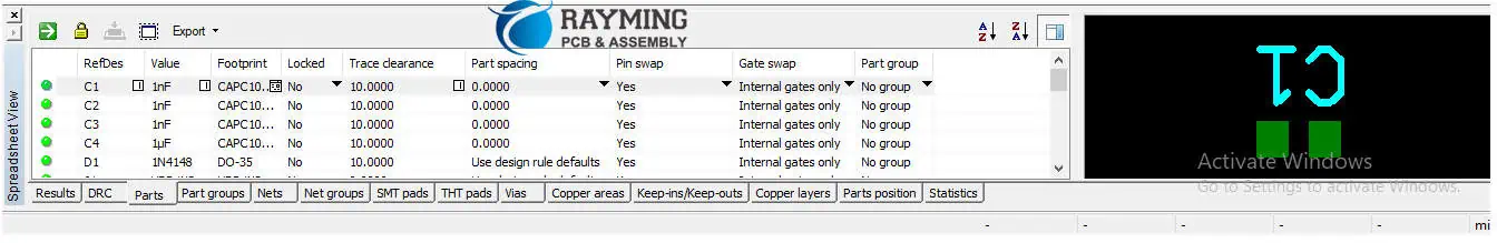
The Bill of Materials is having required information about the entire electronic components which are used in the layout of PCBs. The BOM is also having information of the exact locations where each of the component has been placed. Considering an example of certain PCB having various components at different positions such as T1, R1, and C1 etc. being printed on the layout of PCB, however the manufacturer is not aware of the component being used on these positions. Therefore, BOM list will enable the manufacturer to have an idea of the component being used on these locations being transistor, capacitor, resistor, or inductor etc. The BOM is very important when it comes to the assembly process. However, bear in mind that BOM is a simple excel or text file which has information of all components and its exact location. In case if you don’t like the auto generated format of KiCAD, you can also make the BOM in excel spread sheets yourself with your convenience. The image below is illustrating a simple BOM list extracted from KiCAD.

KiCAD

The image above has a total of four columns i.e. Comment, Designator, Footprint, and LCSC Part Number. The Comment is indicating the parts used in the PCBs with its actual values. It describes each component in detail with exact values such as a capacitors C1, C2, C3, and C4 having same values of 0.1uF. However, some of other information must also be catered such as tolerance and voltage allowing capacity etc. Designator is describing the components which are placed at different points. For example, capacitors of values 22pF are placed at points C5, and C6. PCB Footprint is of great importance because the packages in SMD parts are coming in different sizes, and hence the assembling engineer must be knowing which package is going to be best fit in the Printed Circuit Board.

Therefore, the assembly engineer must be aware of the different sizes SMT which are used in the PCB design such as 0603, 0805, and 1206 etc. LCSC Part Number is the column having information for speeding up the process of assembly of PCBs and getting precise results. Each component of the PCB has a unique number through which it is recognized and there is usually a stock of components with each PCB manufacturer. Therefore, this unique component number is very keen in recognition of the component being used and if still there exist any ambiguity then the component unique number might be searched in the library.

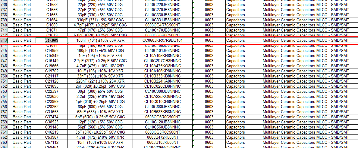
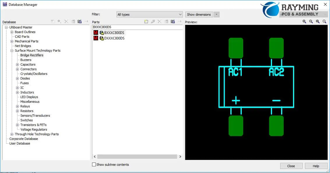
The following image is illustrating the Component number C382097 to be a capacitor having value of 1nF and is to be placed at point C1 on the PCB.

illustrating the Component number C382097

For the purpose of exporting the Bill of Materials from KiCAD tool, you are required to click or go to the script of Arturo’s BOM export. You can easily find it on the web. Download the script which is usually in ZIP form and then unpack it. The image below is illustrating way to acquire the Arturo’s BOM script, downloading, and installation of the script.

illustrating way

After the installation of the script, open it and then click on the option of Export BOM for the specific PCB required. You have to add the BOM script in to the KiCAD PCB file which is opened. From the command window of the KiCAD tool, change the command to %O.csv from the command %O and then click on the generate BOM for its generation. This is going to generate the required BOM which is required for the PCB Assembly process. The figure below is demonstrating the method described above for changing the command and then generation of BOM.

demonstrating the method

The Generation of Component Placement List from KiCAD Tool

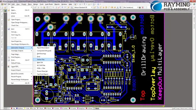
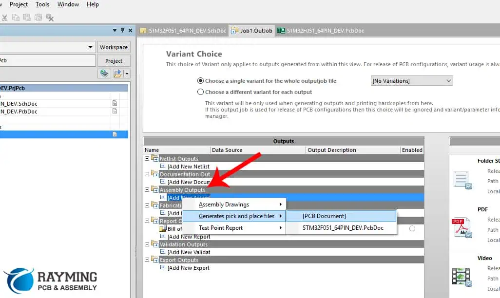
As described earlier that the Component Placement List which is also known as Pick and Place list of the component can also be generated from KiCAD tool. Therefore, for CPL list acquisition, first of all the PCB editor needs to be opened. By clicking on the “File” option in the PCB editor, go to the option “Fabrication Output” and then click on the “Footprint Position”. The footprint position is in .pos format. You have to export the file and then change it with the settings shown in image below.

export the file and then change it

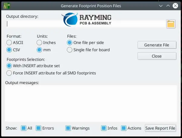
First of all you need to change the format of the file to “.csv”, change the required units in to “mm”, and “One file per side”. After this, you have to select the footprint selection to “with INSERT attribute set”. At the end you have to click on the all options given at bottom of tab i.e. “all, errors, warnings, infos, and actions”. At the end click on “save report file”, however give proper location where the file has to be saved.

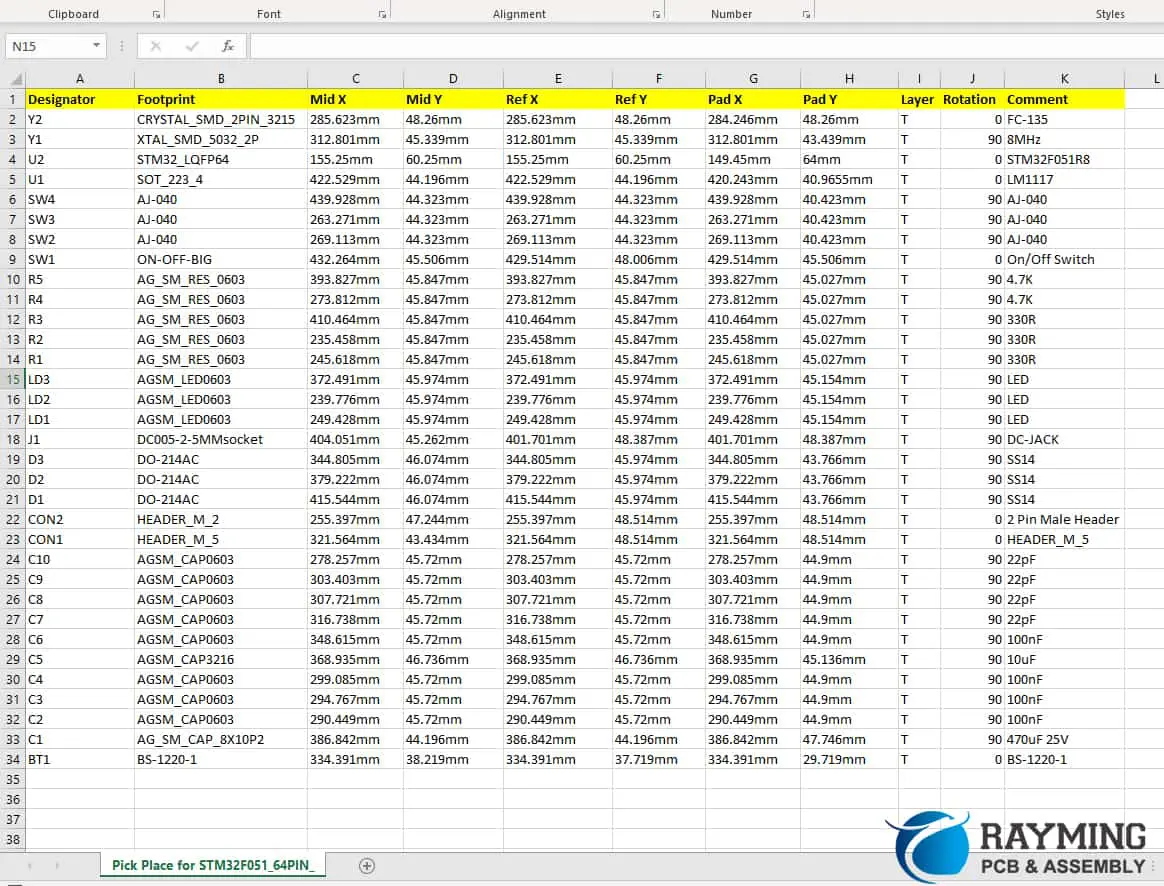
For having a compliance with the RayPCB SMT, you are required to edit the Component Placement List file libreoffice Calc. or excel format. Therefore, for the purpose you are required to do the changes as described below.

First of all you have to ref to the designator of PosX to that fo Mid X PosY to Mid Y Rot to Rotation Side to Layer, before making the export form the KiCAD tool.

KiCAD tool.

After the modification of the header, you will get the file with following format illustrated in image below.

modification of the header

Introduction

KiCAD is a popular open-source Electronics Design Automation (EDA) software suite used for Printed Circuit Board (PCB) design. It provides schematic capture and PCB layout functionality along with various other features for electronics engineers. One of the most useful features of KiCAD is its ability to generate manufacturing output files like centroid files, bill of materials (BOM), Gerber files, etc. These files are essential for PCB fabrication and assembly. In this article, we will focus on the method to generate two key output files from KiCAD – the centroid file and the BOM.

Centroid File

The centroid file provides the center coordinates or centroids of all PCB footprints. It is required by the pick and place machine to accurately place components on the PCB board during assembly. Here are the steps to generate the centroid file in KiCAD:

1. Creating Footprints with 3D Models

The first step is to assign 3D models to all the footprints used in the PCB layout. The centroid data is extracted from these 3D models. KiCAD includes many pre-defined 3D models and you can also create custom models.

2. Enabling 3D Viewer

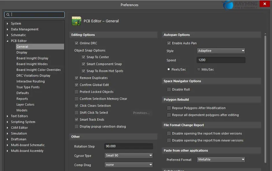
The 3D viewer must be enabled in PCBNew to render the board with 3D models for generating the centroid file. This can be done by going to Preferences > 3D Viewer and checking Enable 3D Viewer.

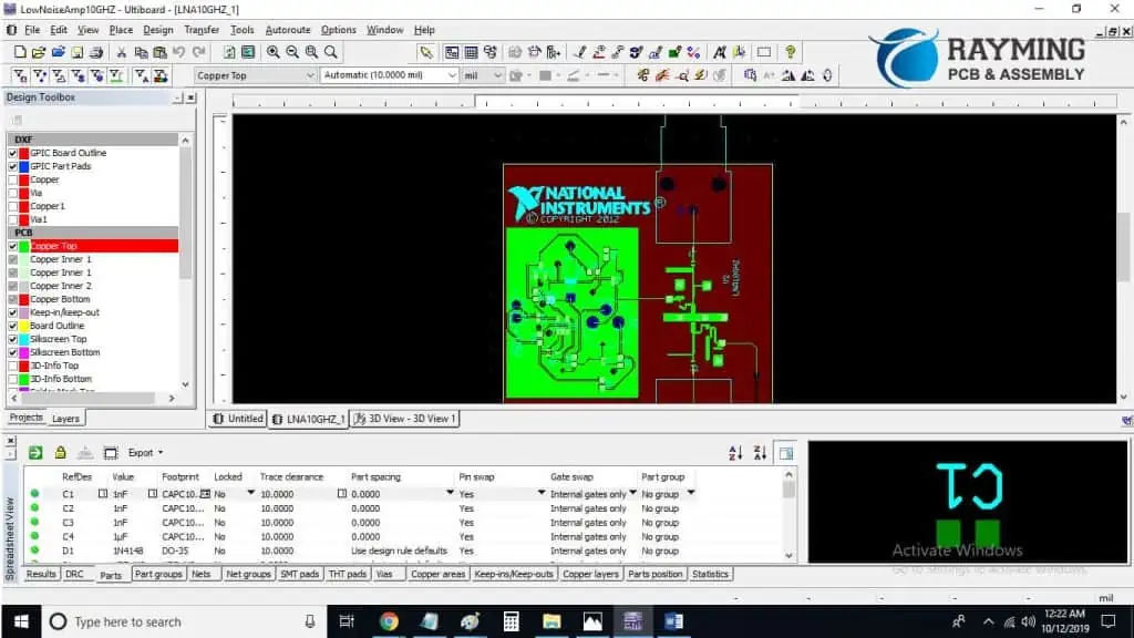
3. Running the 3D Generator

Go to Tools > Generate Fabrication Output. This will open up the fabrication output job editor. Under the General Options tab, enable the following:

  • Force recreate files
  • Use complete suffix
  • Use 3D models
  • Generate centroid info

This will regenerate all the manufacturing files including the centroid data when the job is run.

4. Executing the Job

Click on the Generate button and the fabrication job will be executed. This will generate centroid info in a file named <filename>_centroid_info.csv along with other fabrication outputs.

The centroid file can be found under the main project folder. It contains a list of all footprints along with their reference designator, center X, Y coordinates and rotation angle. These coordinates should match the 3D models visible when the 3D viewer is enabled.

Bill of Materials (BOM)

The BOM or bill of materials is a list of all the components used in a PCB along with key information like reference designator, description, quantity, etc. The BOM acts as a shopping list for purchasing components for production. The following steps describe how to generate a BOM from KiCAD schematics:

1. Associating Components with Schematic Symbols

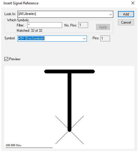
For each component in the schematic, make sure to associate it with a schematic symbol and provide a unique reference designator. This information will get populated in the BOM.

2. Including Part Information

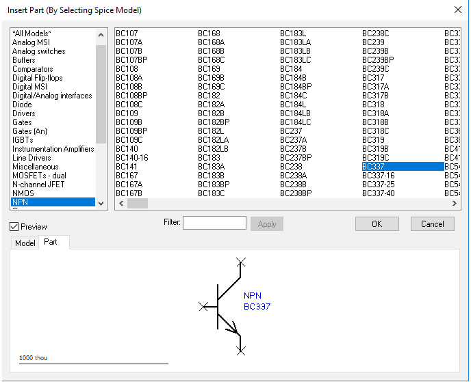
Add complete part information like manufacturer name, part number, description, etc. for each component in the schematic. This data can be entered in the component’s properties window.

3. Assigning Field Names

KiCAD allows mapping the part fields like description, part number, etc. to specific column headers in the BOM. This can be configured in the schematic editor preferences.

4. Generating Netlist

Before generating BOM, you need to create a netlist to synchronize the schematic and PCB. Go to Tools > Generate Netlist to create the netlist file.

5. Using Component Class Dialog

The component class dialog in PCBNew is used to classify components into various types like integrated circuits, resistors, capacitors etc. This classification can be used to group components in the BOM.

6. Generating BOM

Finally, go to Tools > Generate Bill of Materials to create the BOM. This will generate a .csv file containing the reference, quantity, description, part number and other fields for all components.

The BOM can be customized further by editing the template or XSLT stylesheet used for BOM generation. Fields can be added, removed or rearranged as per requirements.

Additional Points

Here are some additional points to keep in mind while generating BOM and centroid files:

  • The fabrication output generator provides many options to customize the outputs as per board house requirements.
  • The Reference Reference column can be used in the BOM to cross-reference components from schematic to PCB.
  • The position and rotation column in BOM provides placement info that can be used during assembly in combination with the centroid file.
  • Multiple BOMs can be generated with different grouping and filtering criteria.
  • The component grouping feature is useful for organizing BOM by component types.
  • Scripting can be used to automate running the fabrication output generator for quick BOM/centroid file creation.

Conclusion

Generating manufacturing files like BOM and centroid data is crucial before sending a PCB design for fabrication and assembly. KiCAD’s fabrication output generator provides an efficient one-step solution to create these files from the PCB projects. Configuring the right options and customizing the output templates allows generating high quality BOM and centroid files that can be readily used by PCB manufacturers. This automated documentation saves significant amount of time and effort while also minimizing errors during the manufacturing process.

Frequently Asked Questions

Q1. What is the importance of a centroid file?

A1. The centroid file provides the center point coordinates of all PCB footprints which are required for accurate component placement by pick and place machines during assembly.

Q2. Can BOM be generated without creating a PCB layout?

A2. Yes, BOM can be created directly from the schematics before PCB layout by using the Generate Bill of Materials tool in EESchema.

Q3. What is the use of component grouping in BOM generation?

A3. Component grouping allows classifying components into categories like ICs, resistors, capacitors etc. This groups components in the BOM making it easier to read and analyze.

Q4. How can the BOM be customized in KiCAD?

A4. BOM can be customized by editing the BOM template and XSLT stylesheet used for generation. This allows changing fields, ordering, grouping etc. as per requirements.

Q5. Is it possible to generate multiple centroid files for different PCB assemblies?

A5. Yes, multiple centroid files can be generated by creating assemblies of boards and footprints. The 3D generator can then output separate centroid files for each assembly.

What is the relationship between DC resistance and AC resistance of a diode?

Top PCB design software

Introduction

Diodes are semiconductor devices that allow current to flow in only one direction. They have unique electrical characteristics that make them useful for a variety of applications such as rectification, switching, clamping, etc. One important parameter that defines the behavior of a diode is its resistance. However, the resistance is not constant and varies with the type of current – Direct Current (DC) or Alternating Current (AC). In this article, we will explore the difference between DC and AC resistance of a diode and the relationship between the two.

DC Resistance

The DC resistance of a diode refers to the resistance offered by the diode to a direct current. It is the ratio of the applied DC voltage across the diode to the resulting DC current through it. Some key points regarding DC resistance:

  • DC resistance arises from the bulk resistance of the semiconductor material used to make the diode. It is relatively low, typically just a few ohms.
  • DC resistance stays fairly constant until the diode starts conducting current in the forward biased condition.
  • Once the diode starts conducting, the DC resistance drops exponentially as the current increases.
  • DC resistance is low in forward bias and very high (ideally infinite) in reverse bias.
  • DC resistance can be derived from the diode’s I-V curve and is equal to the inverse slope of the curve in the linear region before the diode turns on.

DC Resistance vs Forward Current curve for a diode showing low constant resistance initially followed by exponential decrease upon conduction.

AC Resistance

AC resistance refers to the resistance offered by a diode to alternating current. It arises primarily due to the junction capacitance of a diode and differs significantly from DC resistance. Some key points:

  • AC resistance is frequency dependent and varies with the frequency of the AC signal applied.
  • At very low frequencies, AC resistance is high and nearly equal to DC resistance in reverse bias.
  • As frequency increases, AC resistance starts decreasing due to charging and discharging of junction capacitance.
  • The junction capacitance provides a low reactance path for AC at higher frequencies. Hence, AC resistance decreases.
  • At very high frequencies, AC resistance approaches a minimum value known as dynamic resistance.

Variation of AC Resistance with frequency for a diode showing decrease with increase in frequency.

Relationship between DC and AC Resistance

From the characteristics described above, we can summarize the relationship between DC and AC resistance as follows:

  • At very low frequencies, AC resistance ≈ DC resistance in reverse bias
  • As frequency increases, AC resistance decreases while DC resistance remains unchanged
  • DC resistance represents a lower limit for AC resistance but AC resistance can never fall below DC resistance
  • At very high frequencies, AC resistance approaches dynamic resistance which is higher than DC resistance
  • DC resistance is determined by the bulk resistance of the diode material
  • AC resistance depends on frequency and junction capacitance along with bulk resistance

Therefore, we can conclude that AC resistance is always greater than or equal to DC resistance for a diode. But the exact relationship varies depending on the frequency. The AC resistance equals the DC value only under static conditions at low frequencies. As frequency increases, the AC resistance starts decreasing due to capacitive effects while the DC resistance remains constant.

What causes the difference between DC and AC resistances?

The key factors that cause the DC and AC resistances to be different are:

1. Junction Capacitance

  • Every PN junction has an inherent junction capacitance which depends on the area of the junction, doping levels and voltage applied.
  • In reverse bias, the depletion region at the junction acts as the dielectric of a parallel plate capacitor causing capacitance.
  • Under AC, this capacitance provides a reactive path for the current to flow by charging and discharging.
  • Hence, AC resistance decreases with increase in frequency due to capacitive reactance.

2. Minority Carrier Injection

  • Under DC, only majority carriers contribute to conduction which depends on the bulk resistance.
  • But in AC, minority carriers also get injected into the junction when it is forward biased during one half cycle.
  • These extra carriers increase the conductivity and lower the dynamic resistance under AC conditions.

3. Temperature Effects

  • DC resistance has a positive temperature coefficient – increases with temperature due to higher lattice vibrations.
  • But AC resistance and capacitance are negatively affected by temperature rise.
  • So heating causes DC resistance to increase but AC resistance decreases due to reduced capacitive reactance.

4. Non-linear I-V Characteristics

  • The diode does not follow Ohm’s law. Instead it has an exponential I-V relationship in forward bias.
  • So AC resistance becomes dependent on the operating point unlike the DC case.
  • Significant non-linearity causes DC and AC resistances to diverge.

5. Transit Time Effects

  • At high frequencies, the diode’s transit time for carriers starts affecting the AC resistance.
  • Transit time acts as a small inductance, thereby increasing impedance.
  • Thus transit time effects also contribute to the difference between DC and AC resistances.

How are DC and AC resistances specified in diode datasheets?

Diode datasheets often provide the following resistance specifications:

ParameterDescription
Forward resistanceDC resistance in forward conduction
Reverse resistanceDC resistance in reverse bias
Dynamic resistanceMinimum AC resistance at high frequencies

Additional details provided:

  • DC resistances are specified at a particular forward current and reverse voltage.
  • Dynamic resistance is specified at a test frequency, usually 1 MHz.
  • Junction capacitance values are provided as a function of reverse voltage.
  • Forward resistance is represented by slope of forward I-V curve.
  • Temperature dependence of resistances is also specified.
  • Switching times and transit times indicate high frequency limitations.

By combining the DC resistance, junction capacitance and other parameters, the AC resistance at different frequencies can be estimated.

Applications exploiting the DC and AC resistance properties

The difference between the DC and AC resistances of a diode is useful for the following applications:

Rectification

  • Low DC resistance in forward bias allows high DC currents for rectification.
  • High AC resistance in reverse bias blocks reverse AC voltages.

Switching and Clamping

  • Fast switching between low and high resistance states allows using diode as switch.
  • Varying AC resistance helps in waveform clamping and shaping.

Radio Frequency Detection

  • Variation of AC resistance with frequency is useful for detection of RF signals.
  • Diode resistance matches to load at signal frequency for good impedance matching.

Reverse Leakage Control

  • High DC resistance in reverse bias minimizes reverse saturation current.
  • This reduces leakage and improves performance.

Temperature Sensing

  • DC resistance change with temperature is utilized for sensing.
  • AC resistance change is relatively lower, hence does not affect temperature sensitivity.

Conclusion

To summarize, DC and AC resistances are two different diode parameters that are related but not equal in magnitude. DC resistance represents the static bulk resistance while AC resistance is frequency dependent due to capacitive effects. AC resistance equals DC resistance only at very low frequencies and starts decreasing as frequency rises. The difference arises due to factors like junction capacitance, minority carrier injection, temperature effects and transit time. Diode datasheets specify DC resistances along with parameters like capacitance and transit time to allow estimating AC resistance. The variation between DC and AC resistances is exploited in applications like rectification, switching, clamping, RF detection and temperature sensing. Proper understanding of the relationship between the two resistances is therefore important for selecting the right diode for different applications.

Frequently Asked Questions

Q1. Why does AC resistance decrease with increase in frequency?

Ans: AC resistance decreases with increase in frequency because of the junction capacitance of the diode. At higher frequencies, the capacitive reactance XC becomes low, providing an alternate lower resistance path for AC current to flow through capacitance by charging and discharging effect.

Q2. Is AC resistance affected by temperature?

Ans: Yes, AC resistance is affected by temperature. Increase in temperature causes the junction capacitance to decrease due to increase in intrinsic carrier concentration. This causes the AC resistance to increase with temperature.

Q3. Is AC resistance higher or lower than DC resistance?

Ans: AC resistance is always higher than or equal to DC resistance. It equals DC resistance only at very low frequencies when capacitive effects are negligible. At higher frequencies, AC resistance becomes lower than DC resistance due to capacitive reactance but never falls below the DC resistance value.

Q4. Does a diode follow Ohm’s law?

Ans: No, a diode does not follow Ohm’s law. It has an exponential I-V relationship in forward bias due to its PN junction properties. This non-linear V-I curve causes the AC resistance to become dependent on the operating point.

Q5. Why does transit time affect AC resistance?

Ans: At high frequencies, the diode’s transit time for charge carriers starts affecting the AC resistance. Transit time acts as a small inductance that increases impedance and hence increases AC resistance at very high frequencies.

How to Explort Gerber Files from Kicad

Kicad PCB

Introduction

KiCad is a popular open-source printed circuit board (PCB) design tool used by engineers and hobbyists. After completing a board layout in KiCad, manufacturing output files called Gerber files need to be generated to hand off for PCB fabrication. This article provides a step-by-step guide on properly exporting Gerber files from a KiCad PCB design including setup, configuration, layer mapping, and validation checks.

Overview of Gerber Files

Gerber files are the standard image format used by PCB manufacturers to represent copper layers and other fabrication data for photolithographic reproduction. Key facts about Gerber files:

  • 2D vector images defining PCB layer artwork geometries
  • Each layer such as copper, silkscreen, solder mask outputs as a separate file
  • Contains photoplotter commands to image shapes in each layer file
  • RS-274X file format standardized by Gerber Group
  • Requires specific mapper settings to generate properly from CAD tools

Correctly configured Gerber files are required for the PCB fabrication house to produce the design as intended.

Before Exporting Gerbers from KiCad

Figure 2 Gerbers Settings Dialogue Box

Prior to exporting Gerber files, it’s important the KiCad PCB design is fully complete and validated through:

  • All routing and layout changes finished
  • Electrical rule check (ERC) passed with no errors
  • All footprints updated to match sourced components
  • Design rule check (DRC) passed with no errors
  • 3D visualization checked for errors and clearances

Any layout changes made after generating Gerbers won’t be reflected in the files. It’s vital to freeze the design prior to Gerber export.

Step 1 – Validate Design Rules

The first step is running a full design rule check:

  1. Open the PCB file in KiCad and select Design Rules from the toolbar.
  2. In the Design Rules window, browse each rule category like Routing, Sizing, Masks etc.
  3. Verify all settings like track width, clearance, annular ring size, and mask margins meet fabrication requirements.
  4. Click OK after confirming rules are set as needed for manufacturing.
  5. Run Tools → Design Rule Check and resolve any errors before proceeding.

Correct design rules prevent errors like trace sizes or spacings that violate fabrication limits.

Step 2 – Generate Drill Files

The Excellon drill files defining hole sizes and locations are exported first:

  1. With the PCB open in KiCad, go to File → Fabrication Outputs → Drill Files.
  2. Choose a directory to save the drill files and enter a Drill File Prefix like ‘boardname-RoundHoles’.
  3. Select ‘File Format’ as Excellon 2′.
  4. Set ‘Map Files’ to ‘PTH and NPTH into single file’ for combining plated and non-plated holes.
  5. Enable ‘Minimal header’ and ‘Mirror y axis’ options.
  6. Click ‘Generate Drill File’ to create the Excellon NC drill file.

These steps properly configure the Excellon file expected by fabrication shops.

Step 3 – Generate Gerber Job File

  1. Staying in the Fabrication Outputs menu, next click ‘Gerber Files’.
  2. Select ‘Protel filename conventions’ since this matches how KiCad maps layers.
  3. Choose a directory to store output files and enter a File Name Prefix like ‘boardname’.
  4. Click ‘Generate Gerber job file (RS-274X)’ to create a .gbrjob project.

This .gbrjob file will configure and contain all the PCB layer Gerber files.

Step 4 – Map Layers to Gerber Files

Within the .gbrjob, map PCB layers to Gerber files:

  1. Double click the .gbrjob in File Explorer to open the Cam Processor job.
  2. In the Layers/Files map table, click each ‘File’ cell and set the corresponding file name (F.Cu, B.Cu, etc).
  3. Verify each PCB layer maps to the expected Gerber file based on standard conventions.
  4. Click each file hyperlink to validate proper file extensions like .GTL, .GTO, and .GTP.

mapping or extension could cause fabrication errors.

Step 5 – Generate Gerbers

With layer mapping configured, now generate Gerber files:

  1. In Cam Processor, click the Process Job button.
  2. A prompt will warn if there are any unmapped layers detected. Ensure all layers show a mapped file.
  3. Click OK to start Gerber file generation.
  4. The job log will display each layer file as its generated.
  5. After completion, click Close to exit Cam Processor.

The needed Gerber fabrication and assembly files are now created!

Step 6 – Validate Gerbers

Before sending to fabrication, validate the files:

  • Visually inspect each layer file in a Gerber viewer. Check for any missing copper or openings.
  • Confirm all file names match chosen convention like .GTO, .GTS, .GTL, etc.
  • Verify file polarity (dark/clear) came out as expected
  • Load files into CAM software like FlatCAM for additional checks and DFM analysis
  • Confirm board outline matches mechanical layer with no unwanted opened cutouts

Fixing issues in the source PCB design is needed if any discrepancies are observed.

Gerber File Function

Rs 274x Gerber Files Format

Here are the typical Gerber files generated from KiCad and their purpose:

FilePurpose
.GTLTop layer copper
.GBLBottom layer copper
.GTSTop soldermask layer
.GBSBottom soldermask layer
.GTOSilkscreen print legend layer
.GTPSolder paste layer
.GNDBoard profile contour
.DRDNC drill file

Configuring Gerber Export Settings

Several export options are available under File → Fabrication Outputs:

  • Units – Inches or millimeters
  • Precision – Number of decimal places in output files
  • Polygon filling – Smooth filled regions or hatched polygons
  • Gerber extensions – Change from standard .Gxx if required
  • Exclude PCB edge layer – Omit board mechanical outline
  • Subtract mask from silk – Remove soldermask below silkscreen text
  • Drill Units – Inch or mm Excellon format
  • Mirror axes – Flip plot to traditional Gerber orientation

Ensure options match requirements of the target PCB fabrication shop.

KiCad Gerber Generation – FAQs

Here are some frequently asked questions about generating Gerber files from KiCad:

What is the standard Gerber mapping convention?

KiCad follows the Protel filename convention like .GTL for Top Layer where the first letter indicates layer and second letter indicates function.

How can Gerber files be validated?

Use a free Gerber viewer like the one built into FlatCAM to visually inspect each file layer, check polarity, confirm board outline, etc.

Do Gerbers require a specific coordinate origin?

The origin set under File → Page Settings when creating the KiCad project will establish the coordinate system zero reference for output files.

What if KiCad is missing needed layers?

Not all fabrication layer types like non-plated holes or finishing notes have default mappings. Custom Gerber jobs can add mappings for any additional files.

How are internal cutouts and holes represented?

KiCad outputs cutouts, slots, and holes as clear polygons or regions in each respective layer file. No additional drill or aperture info is needed.

Conclusion

Exporting properly mapped and validated Gerber files from KiCad provides PCB fabricators the manufacturing information they need to accurately produce a board design. Configuring the layer-to-file mapping table along with output settings generates the correct fabrication files expected from CAD tools. Visually inspecting layers and running design rule checks verifies completeness before release. Taking care to meet Gerber format requirements avoids delays, added costs, or impediments during PCB production. Manufacturing can proceed smoothly with clean verified Gerber output from KiCad designs.

How to Generate Bom and Centroid File from Altium ?

Altium vs Cadence

Introduction

Altium Designer is a popular printed circuit board design tool used by electronics engineers. Two crucial outputs needed from the PCB design process are the bill of materials (BOM) and centroid data file. The BOM lists all components required to build the board while the centroid file provides pick and place machine information on component locations. This article covers how to properly generate and export the BOM and centroid file from an Altium PCB design.

Bill of Materials (BOM)

The bill of materials is one of the most important documents needed to manufacture a PCB assembly. The BOM lists all components required for production along with key details like:

  • Component designators – Unique IDs like R1, C5, U3 etc.
  • Description – Component name/value like “10uF capacitor” or “1N4148 diode”
  • Library reference – Part number matching supply chain naming
  • Quantity – Total amount needed of each component
  • Reference prefix – Code indicating component family like R for resistor
  • Supplier/Manufacturer – Vendor names for sourcing parts
  • Packaging info – Reel, cut tape, tray styles for assembly planning

The BOM provides procurement and the assembler every component required in the right quantities to build the board along with vital attributes to ensure the correct parts are sourced.

Centroid File

The centroid file provides exact X-Y location coordinates for every component to facilitate automated pick and place assembly. Key centroid data includes:

  • Designator – Identifying part code like C7 or U12
  • Center location – X and Y position relative to assembly origin
  • Rotation – Angle of rotated parts
  • Description – Component name and value

This coordinate information allows SMT assembly machines to precisely place components onto PCBs.

Exporting BOM and Centroids from Altium

Altium provides dedicated tools to generate manufacturing BOM and centroid files:

Bill of Materials

  1. Open the compiled PCB document in Altium.
  2. Go to Reports -> Bill of Materials to open the BOM dialog.
  3. Select the needed BOM template like Manufacturing or Procurement.
  4. Choose output format like CSV, Excel, etc.
  5. Set output file save location from dialog or project folder.
  6. Click OK to run generate BOM report.

The BOM can be further processed in spreadsheets if needed for supply chain integration. Detailed fields and custom company templates simplify BOM generation.

Centroid File

  1. With PCB open in Altium, go to File -> Fabrication Outputs -> Centroid File.
  2. Choose file type like CSV or Excel.
  3. Set options like units, precision and rotation format.
  4. Specify filename and location to save centroid data.
  5. Click OK to generate centroid file.

The flexible process supports both through-hole and SMD components. Advanced selections like grouping parts into batches for panelized assemblies is also possible.

BOM Settings and Configuration

BOM of PCB Assembly
BOM of PCB Assembly

Several options exist to tune the exported BOM:

BOM Templates

  • Use dedicated procurement and assembly templates to include required data
  • Leverage custom company templates aligned to ERP needs
  • Specify all component parameters needed by assembly vendor

Parameter Filters

  • Control which design data parameters show up for each component
  • For example, include packaging for procurement but not electrical specs

Designator Sorting

  • Set ordering like reference prefix or component type grouping
  • Optimized sequence reduces placement changeover during assembly

Board Variants

  • Generate separate BOM for each assembly variant if using design reuse
  • Ensure only components on a specific variant are included

Proper BOM configuration reduces errors and manual efforts needed for manufacturing handoff.

Centroid Settings

Key options when generating centroid data:

Units

  • Specify millimeters (mm) or inches (mil) for coordinate values

Rotation

  • Degrees or radians options for rotated part angles

Fields

  • Customize centroid file headers like including package size info

Precision

  • Set number of decimal places for coordinate values

Layer Types

  • Include centroids for: top, bottom, both layer parts

Origin

  • Define (0,0) board reference location (e.g. lower left)

Correct centroid file configuration avoids issues during automated assembly.

Validating Outputs

Before sending BOM and centroid files to manufacturing, carefully check:

BOM Validation

  • All components show up in BOM
  • Designators match schematic
  • Part numbers align with central library
  • Quantities needed are accurate
  • Parameters like package and supplier populate
  • Review for any duplicate or missing entries

Centroid Validation

  • All components have centroid data
  • Coordinates accurately reflect design placement
  • Rotation angles match component orientation
  • Units and precision are as expected
  • Spot check locations of a few footprints

Verifying the outputs matches expectations avoids incorrect or incomplete information being sent to procurement and assembly.

BOM/Centroid Generation Automation

Manual BOM and centroid file generation can be automated and streamlined in Altium using:

  • PCB Panels – Output all boards in a panel array in one action
  • Design Rule Checks – Execute BOM and centroid run as part of manufacturing DRC validation
  • Scripts – Write scripts to automate BOM and centroid file output
  • Version Control – Integrate into ECO release processes and versioned outputs
  • Output Job Files – Configure presets for one click BOM and centroid file output

This reduces repetitive manual actions for a robust manufacturing handoff process.

Source Control and Versioning

Maintaining properly versioned BOM and centroid data is crucial for quality:

  • Store files in source control like Git along with project
  • Include version number in BOM file names like ACME_Widget_A1.2_BOM.csv
  • Track changes to BOM and centroid files in version history
  • Associate file revisions with ECO release processes

This linkage provides full manufacturing component and assembly data traceability.

BOM/Centroid Generation – FAQs

SMT Bom checking

Here are some frequently asked questions around generating BOM and centroid files:

How often are BOM/centroid files updated?

BOM and centroid files should be re-generated anytime the schematic or PCB layout changes. This ensures procurement and assembly always have the latest component information.

What if assembly is outsourced?

The designer still provides the BOM and centroids reflecting the designed board to the contract assembler per their requirements. All supporting data helps avoid errors.

Can BOM reference distributor part numbers?

The BOM links to internal company part numbers. Distributor cross-reference info can be optionally included to aid procurement.

What if the PCB panelizes boards?

Panelized arrays output a single centroid file containing all boards. Software maps components to their locations in the panel for assembly.

How are BOM differences resolved?

The PCB BOM authority over schematic BOM. Any discrepancies are flagged for engineers to resolve component mismatches between tools.

Conclusion

The bill of materials and centroid location data are mission critical manufacturing deliverables from the PCB design process. Altium provides dedicated tools to properly generate and export these files by selecting appropriate templates, configuring settings, and customizing output parameters. Cross-validating the BOM and centroids against source data prevents incorrect manufacturing information that can lead to errors during procurement and assembly. Automating and integrating BOM/centroid file output into release processes and version control further enhances traceability and quality. With clean properly configured datahandoffs, manufacturers are set up for first-time-right production of complex electronics.

BOM/Centroid Generation FAQs

What is the difference between a BOM and a Pick and Place file?

The BOM provides the list of components and quantities needed. The Pick and Place file supplies precise X/Y coordinate locations for automated assembly. Both are required from PCB design tools.

What is the typical process for generating BOMs?

BOMs are initially created by the PCB designer then often passed to manufacturing engineers to review and add any missing fabrication and assembly information before release.

How can part reference designators be kept aligned between CAD tools?

Unique component IDs like R27 or C122 should be assigned in the schematic CAD then imported to the PCB layout tool rather than renumbered.

Is supply chain integration used for BOM generation?

BOMs can link to part catalogs, company databases, and ERP systems to automatically pull manufacturer part numbers, datasheets, pricing etc.

How are BOM revision levels maintained?

PCB design tools integrate with version control systems like Git to save BOM file revisions synchronized with project commits providing full version traceability.

Generating Step by Step

Method for Generation of Centroid File and Bill of Material from Altium

Altium tool is very handy in the generation of Bill of Material (BOM) and Electronic Component Placement List (CPL) which is also referred as Centroid file. The following is the way to go.

All you need to know about Bill of Material

The BOM file is telling the manufacturer about the components which must be installed on the PCB. The BOM is also having information of the exact locations of the components. For instance, there are different points on PCB such as T1, R1, and C1 etc. which depicts the location of components such as resistor, capacitor, inductor, and transistor etc. The information is present in the Bill of Material file and is very important for the assembly process. BOM is generally a simple text format file to be opened in excel having comma separated (CSV) form. This file can also be opened in any other software tool supporting spreadsheets. The following figure is an example of BOM file.

an example of BOM file.

From the figure above, it can be seen that the first column is having information of the values of capacitors and the column is named as “comment”. The comment section should have as much details as possible such as tolerance and maximum allowable voltage information etc. This is for allowing the manufacturing staff to have information of the perfect component to be used for the project. The next column name is “designator” which has information of the position of the component on PCB so that component is soldered at accurate place. Third column is “footprint” and it is also referred as “package” having information of the SMD components having different sizes. Therefore, manufacturing staff is able to know about the size of component to be best fit for PCB. There are different sizes of the SMT components such as 0603, 1206, and 0805 etc. The last column is named as “LCSC part number” which carries information for speeding up the process to get accurate results. RayPCB is having a very large library of components having a unique number. These unique part numbers can be utilized for the identification of accurate part needed.

For saving time in forthcoming projects, the “LCSC part number” can also be added in to the CAD software. In this way when the BOM list is generated next time, the components will be assigned with their unique numbers and it will save time in future.

This article is having detailed information of adding the LCSC part number in Altium tool, however same can also be done in other EDA tools as well. First step is opening of the integrated library project which has the required parts such as capacitors, resistors, and inductors etc. The file is named with any unique name such as XBASIC. However, this project is containing two major parts i.e. the schematics symbol and the other is PCB footprints. The file with the symbols of schematics should be opened having an extension (.SchLib). Next step is going to the tab of schematics library.

schematics library

The tab is having information of all required parts in the library, for instance by selecting the SMD Ceramic Capacitor having 0603 size, double clicking it will open up its entire properties.

SMD Ceramic Capacitor

Now, in the area of parameters, you have to click on the “add” option for adding the new parameter for the part. This can be illustrated in image below.

“add” option

After this adding the new parameter is done. Now name it as “LCSC Par # XX” and then put the designated value for the part such as “C0000”.

LCSC Par # XX

The value of the LCSC part number form can be acquired from the website of RayPCB as there is a list of about 35,000 different components.

 35,000 different components

Similarly, the LCSC part number can be added in to all of the parts of the project easily to make the assembly process of future projects smooth.

Generation of Bill of Material File

The Bill of Material can also be generated like all other files such as drill and gerber files. The BOM file is generated with the help of “output job file” when Altium tool is considered. Therefore, the use of output job file must be incorporated.

Click on the projects, go to “add new to project” and then select the option of “output job file” as illustrated in figure below.

add new to projec

By choosing options above, job file will be added to the project underway and while using it you are able to generate numerous output files. Here, special focus is made on the generation of BOM file, therefore it will be discussed.

Therefore, by clicking on “add new report”, selecting “bill of materials” and then choose “project”. This process is shown in figure below.

bill of materials”

In the generation of BOM, there is an option for adding the column with parameters, as shown below.

adding the column with parameters

Generation of Centroid Files

By the use of same output job file, centroid file can also be generated. As discussed already, centroid file is also known as Pick and Place or Placement of Component file. The image below is showing the method.

Pick and Place

Figure below is showing setup for making centroid file.

 setup for making centroid file
 setup for making centroid file

After clicking on the generate content, you have to go to the folder where all files of the project are saved and pick the file named pick place with .csv format.

 named pick place with .csv format.
BOM

How to Avoid Signal Reflection in PCB

Introduction

Signal reflection occurs when an electrical signal encounters an impedance discontinuity along a transmission line, causing a portion of the signal to be reflected back towards the source. This can lead to interference issues like ringing and noise in high speed PCBs. Properly matching trace impedance and terminating lines helps avoid reflections. This article provides an overview of signal reflection causes, effects, calculations, and design techniques to mitigate reflection problems in circuit boards.

What Causes Signal Reflection?

Reflection arises from an impedance mismatch. Wherever the signal line characteristic impedance Z0 changes along its path, some incident signal energy will reflect while the remainder transmits through.

The most common sources of mismatch and reflection in PCBs include:

  • Trace impedance change from differences in width, thickness, or dielectric
  • Stub traces that branch off from main signal path
  • Components with mismatched terminal impedances
  • Improper termination at load end of line
  • Vias that transition between layers with different stackup materials
  • Discontinuities at connections like connectors or IC pads
  • Damage like cracks or cuts in a trace

Minimizing impedance discrepancies along the signal path reduces the likelihood of reflections.

Reflection Effects

When reflections occur on a signal line, several detrimental effects can arise:

Ringing – multiple reflections lead to resonances and ringing artifacts on the signal

Noise – inter-symbol interference from reflected signals appearing at unintended times

Overshoot – excessive peak voltage from constructive interference between incident and reflected waves

Undershoot – sagging voltage dips caused by destructive signal interference

Jitter – timing variations resulting from impedance discontinuities

EMI – radiated interference caused by resonances along the transmission path

Signal Integrity – reflection noise that can degrade receiver performance and contribute to bit errors

Power Integrity – impedance issues that compound power distribution network resonances

Proper impedance control minimizes these reflection issues which are problematic in high speed digital systems.

Transmission Line Theory

To understand and model reflections, we must consider the transmission line model of interconnects:

Where:

  • R = Resistance per unit length
  • L = Inductance per unit length
  • G = Conductance per unit length
  • C = Capacitance per unit length

Together R, L, G, and C define the characteristic impedance Z0 of the line:

When Z0 is constant throughout the path, signals propagate without reflection. Wherever Z0 changes, reflection occurs according to the reflection coefficient Γ:

Where Z1 is the load or intermediate impedance causing mismatch. This model allows calculating reflection severity at each impedance discontinuity.

Reflection Calculations

The reflection coefficient quantifies the portion of signal reflecting back at a impedance change.

For example, consider a 50 Ω transmission line terminated into 75 Ω. Applying the reflection coefficient equation:

Γ = (Z2 – Z0) / (Z2 + Z0)

Γ = (75 Ω – 50 Ω) / (75 Ω + 50 Ω)

Γ = 0.2

This indicates 20% of the incident signal reflects back from the impedance mismatch. The remainder transmits through to the load.

Additionally, the voltage reflection coefficient ρ provides the amplitude of the reflected waveform relative to the incident wave:

ρ = (Z2 – Z0) / (Z2 + Z0)

So in this example, the reflected voltage wave will be 20% of the incoming signal amplitude.

These principles allow quantifying reflection severity for any impedance mismatch along a transmission path.

Avoiding Reflections During Routing

Several PCB routing techniques help reduce signal reflections:

Impedance Matching

  • Maintain consistent trace width based on stackup dielectric to match target Z0
  • Compensate for thickness changes with width tapers
  • Use impedance calculators to design trace geometry

Use Ground Planes

  • Reference to continuous ground layers stabilizes impedance
  • Avoid routing over splits in ground planes

Minimize Trace Stubs

  • Route with shortest connections between drivers and loads
  • Avoid creating stub traces that branch off of signal lines

Symmetric Routing

  • Equal trace lengths for complementary differential pairs
  • Match component placements of differential pairs

Termination

  • Properly terminate trace ends near load impedance
  • Series terminate drivers, parallel terminate loads
  • Avoid unterminated transmission line stubs

Careful routing practices eliminate unnecessary impedance discontinuities and reflections.

PCB Layer Stackup Design

In addition to routing, the layered construction of the PCB impacts impedance control:

  • Minimize layer changes with vias – use direct routes where possible
  • Maximize reference plane layers – avoid splits under critical traces
  • Model reference plane interactions – maintain constant line environment
  • Watch glassweave effects – model actual weave patterns
  • Keep dielectrics consistent – use same materials for core, prepreg, solder mask
  • Model various densities – copper fills can change local impedance

Simulating the actual manufactured PCB stackup is key to predicting impedance and reflections.

Via Design to Limit Reflections

Vias that transition between layers introduce impedance discrepancies and reflections:

  • Model vias in layout tools and account for pad shapes
  • Use smaller drill sizes to reduce Z0 change
  • Avoid routing vias near sensitive crossover nodes
  • Minimize signal layer changes
  • Place ground vias adjacent to signal for shielding
  • Backdrill or stub-eliminate unused via portions

Properly designing vias for the signal path impedance mitigates discontinuity effects at layer transitions.

Terminating Traces

Adding termination resistors absorbs incident signals, preventing reflections:

Source Termination

  • Called series termination
  • Resistor at source isolates driver from reflections

Load Termination

  • Called parallel termination
  • Resistor at load matches line impedance

Split Termination

  • Combination of source and load termination
  • Divides termination resistance value

Terminations should match line impedance and be located as physically close to endpoints as possible.

Simulation and Modeling

Validate designs through electromagnetic (EM) analysis of reflection severity:

  • Model routed traces with actual geometry in layout tools
  • Simulate across frequency range of interest
  • Identify resonant ringing and reflection hotspots
  • Evaluate effects of layer transitions, vias, stubs
  • Verify location and value of terminations
  • Tune layout to reduce resonances

Simulation provides insight to refine layouts by minimizing identified impedance mismatches before manufacturing PCBs.

Signal Reflection Mitigation – Frequently Asked Questions

Here are some common questions related to dealing with reflections in high speed board design:

What is the typical PCB trace impedance?

The most common impedance for signals lines is 50 ohms. This matches cable impedance and provides a good tradeoff between conduction losses and reflections.

When do reflections need mitigation?

Reflections must be addressed whenever fast edge rates under 1-2ns rise time are present on unmatched transmission lines longer than 1/10th wavelength.

How can reflections be observed?

An oscilloscope plots signal waveform ringing and noise caused by impedance discontinuities. Time domain reflectometry (TDR) tools also measure reflections.

Where should source termination resistors be placed?

Series resistors should be located as close as possible to the driver output pin or package to prevent resonances on the line prior to damping reflections.

What values are used for termination resistors?

Terminator resistance should match the trace characteristic impedance (typically 50Ω). Lower values attenuate while higher values reflect more energy.

Conclusion

Signal reflections that can arise whenever impedance changes along a PCB trace are a primary concern in high speed digital design. Using controlled geometries, matched layer stacks, symmetric layout, routed line terminations, and simulation minimizes discontinuities that lead to problematic ringing and noise. With care taken to design, analyze, and validate the transmission environment, signal reflections can be effectively avoided ensuring reliable circuit performance.

Printed Circuit Boards (PCBs) have been the focus of scientist and engineers to bring novel ideas on how to improve the quality of end electronic product. As PCBs play the key role in functionality and performance of any electronic product or device so the perfectly designed PCB layout is highly important. There are many factors that a design engineer must consider while designing a PCB layout and these factors are driven by the requirements of end product.

Like number of layers PCB, size and dimensions of PCB, number of electronic components to be soldered upon PCB, types of components, routing techniques and many other PCB design factors. Among them one of the most important aspect is the “Impedance Matching”. The PCB that is dedicated for the electronic product that is to be used for High frequency application like RF or microwave electronics, then the most critical part of the PCB layout design is to control the impedance of the circuit.

What is Signal Reflection.?

As we are familiar with the phenomena of reflection that when a light ray is incident on the mirror then the light is reflected from mirror’s surface. Another example is water, when light enters the water some of the light is refracted while some is reflected. The same phenomena is with electrical signal. The signal reflection is the phenomena where the source transmits the electrical signal in the signal trace to the receiver/sink and some part of the signal is reflected back from receiver/sink back to the source. This reflected signal can cause signal distortion and oscillation in the circuit.

Why the Signal is reflected..?

The reason for the signal reflection from receiver to the transmitter is the transient impedance caused by the discontinuity in characteristic impedance of signal trace. If the characteristic impedance is uniform through starting from source or transmitter to sink or receiver then there will be no signal reflection. The discontinuity in characteristic impedance of signal trace can be caused by variation in signal trace width, thickness, distance between the trace and the corresponding reference plane and dielectric constant of the substrate material of PCB.

Effects of Signal Reflection:  

Oscillation:

Fortunately, the signal reflected from receiver is always less in strength then the main signal, hence the reflected signal is again transmitted and then again reflected with lesser strength, and hence in this way the signal is diminished slowly but will cause a temporary oscillation.

Overshooting and Undershooting:

If the delay time between the signal transmission and reception is short and the signal transmission is faster and if the previous reflected signal was not given time/delay to diminish and next signal is transmitted then this will cause the signal “peaks”  to accumulate and will cause reflected signal overshooting thus complete failure of the circuit will happen. Similarly if the signal “valley” are accumulated this will cause reflected signal undershooting thus weakening the main signal to cause false clocking or misinterpretation of digital data lines like SDI, SDO, SCLK etc. This overshooting or undershooting can completely destroy the protective diodes at the signal ends.

Signal Distortion:

The reflected signals from receiver end if are strong enough then they can possibly change the logic state of digital circuitry hence the circuit will behave in unanticipated manner. Distorted signal are sensitive towards noise.

How is Signal Reflection Calculated.?

As an example scenario refer to the diagrammatic representation of the signal trace between two points A and B on the PCB.

In the above diagram signal (Vi Voltage and Current Ii) Vi incident from source A to sink B. The characteristic impedance from A to B was continuous but from point B the impedance of signal trace changed hence changing the voltage Vo and current Io transmitted onwards. The characteristic impedance from A to B is Zi while from point B it is Zo. Keeping the picture in view above, for point B looking from left, we can write using ohm’s law as

(1)

Now looking at point B from right, line impedance is now Zo then we can write for Vo as

(2)

Now there are two cases

Case-1: The Impedance is not discontinuous and Zi = Zo

In this case if Zi = Zo then we simply get Vo = Vi means the transmitted voltage is same as incident voltage Vi and no signal is reflected.

Case-2: Discontinuous Impedance Zi ≠ Zo

Now here the incident signal is not completely transmitted onwards because of discontinuous non-uniform impedance of signal trace. Hence some part of the incident signal is reflected back as “Vr”.

Hence we can write

(3)

Now since the reflected current flows in opposite direction so it will be minus from the incident current hence

 (4)

The reflected signal is travelling along the signal trace part with impedance Zi therefore we can use ohm’s law

(5)

Put equations 1, 2 and 5 in 3 we get

(6)

But

(7)

Therefore

(8)

Or

(9)

This term with the impedance is called the reflection coefficient “Rc”.

 (10)

The value of Rc can be from -1 to 1. But ideally Rc should be zero

Methods to Reduce Signal Reflection:

  • The transmission rate or speed of the signal can be decreased so that the oscillation of reflected signal can be minimized and stabilize the circuit’s signal trace
  • The PCB thickness is relatively kept low so as to reduce parasitic capacitances
  • Shorten the signal transmission trace length by carefully arranging number of layers in multilayer HDI PCBs. This can effectively decrease the parasitic inductance to reduce cross talk between signals
  • The number of turns or bends in the signal trace should be kept as low as possible. The signal trace should be in straight line but if the bend is necessary then the bend arc should be at 45O. This helps to reduce EMI radiation
  • Route all important signal lines on same plane to minimize unwanted through holes.
  • The separate ground and power planes should be used for separate regulated power supply for noise reduction in multiple power supply circuit system. This will enhance signal integrity.
  • Apply correct routing topology

Routing Topologies:

The Parallel Topology:

In this structure arrangement, the source is simultaneously feeding the signal to more than one sinks or receivers. All the nodes/receivers connected in parallel or star fashion are synchronized with source. However the separate termination resistance is required for each node/branch and must be compatible with characteristic impedance.

The Series Topology:

Here the one transmitter or source is connected in daisy chain or series fashion the output of one is connected to input of other. A simple series resistor can be placed close to the driving/transmitting/source end to make the impedance at the receiver side compatible with characteristic impedance. The daisy chain branch length should be kept as short as possible. However the signals received at different receiving ends are not synchronized with main transmitter.

Signal Trace Termination:

There are two ways to terminate the signal trace. Either from the source end or from the sink end.

A simple series resistor placed between source and load and close to the source will do the job.

There are 4 ways to make signal termination at load / sink end.

Single resistor parallel termination:

RC Termination:

Thevenin Termination:

Diode Termination:

Differential Pair Termination:

What does a Flyback Converter Do?

Introduction

A flyback converter is a type of switched-mode power supply (SMPS) commonly used in AC-DC power adapters and chargers for consumer electronics. The flyback topology provides an efficient, cost-effective, and compact method for converting AC mains voltage to a lower DC voltage required by many electronic devices.

This article provides an overview of how a flyback converter works along with its key applications and capabilities. Read on for an understanding of the operating principles, transformer action, design considerations, pros and cons, and typical uses of flyback power supplies.

Flyback Converter Overview

A flyback converter provides DC-DC conversion by storing energy in the magnetic field of a coupled inductor then releasing it to the output. Key characteristics include:

  • Provides galvanic isolation between input and output via a transformer
  • Steps down DC voltage from high to low level
  • Can output multiple regulated secondary rails
  • Wide input voltage range capability
  • Requires a relatively small transformer for power level
  • Cost effective topology using fewer components
  • Used extensively in lower power AC-DC power adapters

The flyback design is an isolated variant of the classic buck-boost converter using a coupled inductor rather than discrete inductor and capacitor storage elements. Flyback topology is popular due to its simplicity, efficiency, small form factor, and wide input/output range capabilities.

How Does a Flyback Converter Work?

The flyback converter operation consists of two repetitive phases:

Phase 1: Charge

During the primary switch ON time, input voltage is applied across the transformer primary winding storing energy in its magnetic field. The primary current and magnetic field ramp up linearly. No power is transferred to the secondary side.

Phase 2: Discharge

During the switch OFF time, the stored magnetic field collapses inducing a voltage spike across the transformer windings. This forwarded voltage spike allows current to flow from ground to the secondary side output, thus replenishing charge to the output capacitor and powering the load.

Cyclically charging the magnetic field when the switch closes, then discharging to the secondary side when it opens, allows efficient power transfer isolated through the transformer. Varying the duty cycle regulates the outputs.

The alternating charge and discharge modes give rise to the terminology “flyback converter” since energy is intermittently “flying back” from the transformer primary to secondary in pulses.

Flyback Converter Waveforms

Analyzing the voltage and current waveforms provides further insight into the flyback operation:

Vsw: The switching waveform applied to the primary side transistor. This chops input DC voltage on and off at a high frequency, typically 25 kHz to 1 MHz.

Ip: The primary winding current. Ramps up when the switch turns on as energy is stored in the magnetic field. Drops to zero and may reverse when the switch turns off.

Vs: The secondary winding voltage. The reflected output voltage plus the induced flyback spike used to deliver power to the load.

Is: The secondary winding current delivered to the load. Pulses each flyback interval to replenish charge on the output capacitor.

Vout: The output voltage across the load capacitor. Smoothed DC output relative to secondary GND despite pulsed power transfer.

Careful timing of the magnetization and discharge phases regulates energy transfer to achieve the desired steady DC output voltage.

Transformer Isolation and Windings

The coupled inductor transformer provides critical functionality:

  • Isolation – The lack of direct conductive paths across the transformer provides electrical isolation between primary high voltage input and secondary outputs. This is both a functional and safety requirement for many power supplies.
  • Voltage Transformation – Per the transformer equations, the secondary to primary voltage ratio is defined by the number of respective wire turns. This transformer action enables stepping the primary voltage up or down to the desired level.
  • Energy Transfer – The inductive coupling passes energy from primary to secondary through the common magnetic field. This enables transmitting power despite a lack of direct connections.
  • DC Blocking – The high frequency transformer only passes pulsing AC from the switched input. This blocks DC voltage from reaching the secondary and prevents core saturation.

Careful transformer design is crucial to optimize the voltage transformations, flux levels, coupling, and isolation performance. Multiple secondary windings provide different isolated output voltages from the same converter.

Flyback Converter Design Considerations

Engineers must consider numerous factors when designing a flyback power supply:

  • Desired output voltage(s) and power levels
  • Required voltage and current regulation limits
  • Efficiency and heat dissipation requirements
  • Safety isolation and surge withstand needs
  • Size constraints and transformer core selection
  • Input voltage range specification
  • Environmental factors like temperature and humidity
  • Output ripple and noise requirements
  • Cost targets and component selection
  • Control loop compensation and stability
  • Driver circuitry and isolated feedback
  • Protections from overcurrent, overvoltage, thermal events

Extensive electrical simulations, transformer design analysis, prototyping, and testing are used to iterate and optimize the flyback converter design to meet all product requirements.

Flyback Converter Pros and Cons

The Flyback Converter Topology

The flyback topology provides some key advantages but also has downsides to consider:

Advantages

  • Simple, low component count design
  • Provides galvanic isolation
  • Wide input and output voltage range capability
  • Multiple outputs readily supported
  • High efficiency with advanced control ICs
  • Compact, small transformer size for power level
  • Lower EMI compared to forward converter
  • Readily available reference design kits

Disadvantages

  • Discontinuous output current pulses
  • Requires complex transformer design
  • Associated EMI challenges require filter circuits
  • Output ripple voltage typically higher
  • High voltage stresses on primary switch
  • Aux power winding required for controller
  • Audible noise possible without optimizations
  • Slope compensation needed for stability

Overall, the flyback design represents an excellent balance of size, performance and cost for lower power AC-DC applications.

Typical Flyback Converter Applications

Some common uses for flyback power supplies include:

  • AC Adaptors – Compact plug-in power bricks for laptops, mobile devices, gaming consoles, monitors, TVs, routers, and modems. Output power from 5W to 200W.
  • Chargers – Standalone battery chargers for consumer devices such as phones, tablets, power tools, and electric toothbrushes.
  • Appliances – Providing DC supplies for appliances like microwaves, printers, scanners, coffeemakers.
  • Medical Equipment – Isolated DC power for portable medical devices requiring regulatory safety compliance.
  • Industrial Systems – Providing auxiliary DC power within industrial equipment like PLCs, transmitters, sensors, indicators, and controls.
  • Consumer Electronics – Any device needing an internal AC-DC power supply such as routers, set top boxes, media streamers.

The wide input range, flexible output capabilities, small size, and low cost make flyback converters a workhorse DC-DC conversion technology for consumer and industrial applications under 200W.

Flyback Controller ICs

Dedicated flyback controller ICs simplify implementation and improve performance. Common controllers include:

  • ON Semiconductor NCP101x, NCP102x, NCP103x Series
  • Power Integrations TOPSwitch Series
  • Infineon OPTIGA Series
  • STMicro STPSxx Series
  • TI UCC287xx Series

These ICs provide functionality like:

  • Adjustable output voltage regulation
  • Auto-restart overcurrent protection
  • Slope compensation and loop stability
  • Primary switch drivers or integrated FETs
  • Fault protections and diagnostics
  • Sync rectification drivers
  • Multi-output secondary controllers
  • Flux density limiting and optimization
  • Frequency jittering for EMI reduction
  • Thermal shutdown protection

Advanced controllers handle control loop tuning, protection features, driving the primary FET, and secondary regulation – drastically reducing system complexity compared to discrete flyback designs.

Conclusion

In summary, a flyback converter provides an efficient method for converting an AC mains voltage to a lower DC level required by electronics devices. Storing energy in a magnetic field which is cyclically discharged to a secondary winding enables isolated power transfer across a small transformer. The pulsed flyback architecture is well suited for compact, cost sensitive, lower power adapters making it prevalent in consumer products. When carefully designed and controlled, the versatile flyback topology will continue providing safe, reliable, and efficient AC-DC conversion.

Flyback Converter Frequently Asked Questions

How does a flyback converter compare to a buck converter?

Unlike a buck converter, the flyback provides electrical isolation across the transformer but requires a more complex winding arrangement. The pulsating output current also leads to higher ripple.

What determines the turns ratio of the transformer windings?

The turns ratio between the primary and secondary windings defines the voltage step down/step up ratio according to the transformer volt-second relationship.

What is the difference between DCM and CCM flyback operation?

In discontinuous conduction mode (DCM) the secondary current falls to zero during each cycle. Continuous conduction mode (CCM) has the current always flowing. DCM is more common for lower power flyback designs.

Why are snubbers used in flyback converters?

Snubbers absorb energy from transformer leakage inductance to limit voltage spikes on the switch during turn-off transitions improving reliability.

What causes audible noise issues?

The magnetostriction effect can cause the transformer core material to vibrate and generate audible buzzing. Potting, gluing, lowest switching frequency, and other optimizations reduce audible noise.

How is IoT used in wireless communication?

4g iot

Introduction

The Internet of Things (IoT) relies heavily on wireless communication technologies to interconnect smart devices and objects. Wireless provides the flexible, low-cost connectivity fabric that enables the wide range of IoT applications transforming homes, cities, industries, transportation and more. This article explores how various wireless technologies are utilized in IoT systems and the considerations around selecting the best approach.

IoT Wireless Communication Requirements

IoT solutions have diverse connectivity requirements that span long range, high bandwidth, mesh networking, low power, and mobility:

  • Range – Connectivity of sensors across a home, factory floor, city grid, agricultural field, etc.
  • Bandwidth – Video security cameras require high throughput wireless links.
  • Mesh Networking – Extending reach by device-to-device multi-hop routing.
  • Low Power – Enabling battery-powered operation for years before maintenance.
  • Mobility – Tracking goods in transit or medical assets in a hospital.
  • Scale – Potentially thousands of nodes even in a local IoT network.
  • Cost – Inexpensive wireless hardware to enable mass deployments.
  • Standards – Interoperability across devices from many vendors.

No single wireless technology optimally meets all of these needs. IoT systems utilize multiple wireless protocols combined in a complementary way.

Wireless Communication Protocols for IoT

Several wireless technologies are commonly used for IoT connectivity:

Cellular

  • 2G/3G/4G/5G – Provides wide area connectivity using existing cellular infrastructure. IoT-optimized LTE variants called LTE-M and NB-IoT exist.
  • Benefits – Ubiquitous coverage, mobility, security, bandwidth
  • Limitations – Cost, power consumption

WiFi

  • 802.11 – Ubiquitous wireless local area networking technology. IoT uses low power WiFi variants like 802.11ah.
  • Benefits – Commonly available, supports IP networking, high bandwidth
  • Limitations – Power hungry, limited range

Bluetooth

  • Bluetooth LE – Low energy version of Bluetooth ideal for periodic IoT sensor data.
  • Benefits – Ubiquitous, very low power, low cost, standards-based
  • Limitations – Short range under 100m. Low bandwidth.

LoRaWAN

  • LoRaWAN – Long range, low power wireless protocol using LoRa modulation on sub-GHz bands.
  • Benefits – Long range (kms), low power, secure, operates below 1 GHz
  • Limitations – Lower bandwidth, higher module cost

Proprietary RF

  • Proprietary – Custom wireless protocols using freely available ISM bands like 900 MHz or 2.4 GHz.
  • Benefits – Optimized for specific application needs around range, power, cost.
  • Limitations – Vertical integration required. No interoperability.

LPWAN

  • Sigfox, Ingenu – Ultra narrowband, long range technologies for basic IoT data.
  • Benefits – Long range, low power, low cost connectivity
  • Limitations – Very low bandwidth. Limited data.

This variety of wireless options provides flexibility to match the right connectivity to application requirements.

Key Considerations for Wireless IoT

Key factors to evaluate when selecting wireless technologies for an IoT solution include:

Power Consumption

Battery powered devices may need to operate for years before maintenance. Low power wireless like Bluetooth LE, LoRaWAN, and LPWAN reduce power use.

Range Requirements

Sensors spread across large physical spaces require long range wireless connectivity, even km-scale for rural settings. Cellular, LoRaWAN provide this.

Bandwidth Needs

Video security cameras require WiFi or 4G LTE class bandwidth versus simple temp sensors that just need low bandwidth LoRaWAN uplinks.

Cost Sensitivities

Bluetooth LE provides the most cost efficient wireless modules. LPWAN networks have low subscription costs for massive sensor deployments.

Mobility

Tracking assets in motion requires cellular or WiFi. Fixed assets can use LoRaWAN, Bluetooth LE, or other lower power approaches.

Security Concerns

Public networks require proven secure connectivity like LTE/5G. Private networks on proprietary RF or LoRaWAN also enable encryption.

Interoperability Needs

WiFi, Bluetooth LE, and LoRaWAN are standardized for interoperability. Proprietary RF limits to single vendor deployments.

Combining technologies is common to meet varied connectivity needs. For example, sensors could use Bluetooth LE to a gateway, then LoRaWAN backhaul to the cloud.

Wireless Technologies for Common IoT Applications

Different vertical IoT applications impose unique wireless requirements:

Smart Home – Primarily uses WiFi with supplemental Bluetooth LE, ZigBee, or proprietary mesh networks to link low-bandwidth sensors and smart home devices.

Industrial IoT – Requires multi-km range on private networks with combinations of proprietary wireless, LoRaWAN, and cellular for backhaul. Reliability and security are critical.

Smart Cities – Take advantage of existing infrastructure using 4G/5G networks for connectivity of city assets. LoRaWAN also sees adoption in city-scale deployments.

Agriculture IoT – Connectivity of rural agricultural assets is enabled by LoRaWAN, Sigfox, and proprietary wireless which provide range of up to 10 km or beyond.

Connected Vehicles – Leverage 4G LTE, emerging 5G networks, and on-board WiFi hotspots for vehicles. DSRC provides short range vehicle-to-vehicle links. Bluetooth LE connects in-cabin.

Retail and Inventory – Stores use a combination of WiFi, Bluetooth beacons, RFID, and LPWAN to link devices managing inventory, logistics, and merchandise flow.

Healthcare IoT – Hospitals employ WiFi supplemented by proprietary RF for reliable indoor asset tracking of medical equipment, and Zigbee devices for long battery life.

The diversity of vertical applications demonstrates why IoT takes advantage of nearly the full spectrum of wireless technologies today.

Wireless Communication Protocols for IoT – Comparison

ProtocolFrequencyRangeBandwidthPowerSecurity
2G850MHz, <br> 1900MHzWide areaUP to 0.3 MbpsHighStrong
3G850MHz, <br> 1900MHzWide areaUp to 14 MbpsHighStrong
4G LTESub 1 GHz, <br> 2.4GHzWide areaUp to 300 MbpsHighStrong
5G NRSub 6 GHz, <br> mmWaveWide areaMulti-GbpsMediumStrong
WiFi2.4 GHz, <br> 5 GHzUp to 100mUp to 1 GbpsHighWPA2 Encryption
Bluetooth LE2.4 GHzUp to 50mUp to 2 MbpsVery Low128-bit AES
LoRaWANSub 1 GHz2 – 15 km0.3 – 50 kbpsVery LowAES 128 Encryption
SigfoxSub 1 GHz3 – 50 km100 bpsVery LowProprietary
Proprietary ISM RF315/433/868/915MHz, <br> 2.4GHzUp to 2 kmUp to 1 MbpsLowCustom Security

Optimizing Wireless Coexistence

With various wireless technologies potentially deployed in proximity, steps must be taken to minimize interference between protocols sharing frequency bands:

  • Proper RF site survey and planning of wireless coverage areas
  • Frequency channelization optimization and allocation
  • Transmit power level adjustments to minimize overlap
  • Scheduling of transmission activity windows
  • Prioritizing co-located traffic based on quality of service needs
  • Adding physical isolation between nearby wireless infrastructure
  • Leveraging directional antennas and spatial separation

Testing and adjustments after deployment can optimize coexistence and performance.

The Role of LP-WAN for IoT Wireless Connectivity

LP-WAN (Low Power Wide Area Network) technologies like LoRaWAN and Sigfox provide a uniquely optimized combination of long-range wireless connectivity and low power operation:

  • Enable battery lifetimes up to 10 years from a single AA battery
  • Provide wireless coverage across entire cities, agricultural areas, and industrial sites
  • Operate in license-free sub-1GHz frequency bands
  • Leverage a star network topology with distributed gateways
  • Offer strong security and interference resistance
  • Support millions of end node devices
  • Enable low cost connectivity at approximately $5 per node
  • Sustain excellent range even in urban areas and indoor locations
  • Provide sufficient thoughput for typical IoT sensor data
  • Maintain robustness at very low transmit power levels

LP-WAN fills a technology gap between short range protocols like Bluetooth LE and wide area cellular networks. This drives adoption for water metering, asset tracking, agricultural monitoring, and smart city applications.

Future Outlook for Wireless IoT Connectivity

The landscape of wireless technologies for IoT continues to rapidly evolve:

  • 5G will provide higher performance cellular connectivity especially benefiting high bandwidth video and mobile IoT uses
  • WiFi 6 increases speed, density, and efficiency of wireless local networking for IoT
  • Bluetooth 5 improves range, broadcasting, and mesh capabilities of Bluetooth LE
  • Thread and Zigbee will gain adoption in smart home and building automation
  • NB-IoT and LTE-M extend cellular capabilities for low power wide area IoT
  • Carrier aggregation across multiple wireless protocols to enhance reliability and throughput
  • Edge computing will distribute intelligence into the IoT network lowering wireless data needs
  • New spectrum like CBRS and 6 GHz bands will expand available wireless capacity

Conclusion

IoT is driving adoption of a diverse palette of wireless technologies to serve the connectivity needs of smart objects. Factors around power, range, bandwidth, mobility, scale, and cost dictate the optimal wireless approach for specific applications. Ongoing enhancement of wireless protocols and spectrum availability will support the growth of IoT innovations transforming our infrastructure, industries, homes and cities. Comprising the communication fabric tying everything together will be standards-based, IP-connected wireless networks enabling the promise of the Internet of Things.

IoT Wireless Communication – Frequently Asked Questions

What is the difference between LPWAN and WAN?

LPWAN refers to Low Power Wide Area Network technologies designed specifically for wireless IoT sensors. This includes LoRaWAN and Sigfox. WAN more broadly means any wide area network including cellular networks.

Which wireless technology has the longest range for IoT?

Sigfox and LoRaWAN can provide wireless connectivity exceeding 50km in rural areas. Proprietary sub-GHz networks can also attain multi-km ranges suitable for wide area IoT.

Do IoT devices support WiFi?

Some do – WiFi provides high bandwidth wireless connectivity suitable for IoT video cameras, gateways, and devices requiring faster data rates. Low power WiFi variants help address high power consumption.

What is 5G NR?

5G NR stands for Fifth Generation New Radio. It defines the global standard for upgraded 5G cellular networks with benefits like multi-Gbps speeds, ultra low latency, and improved support for massive IoT device density.

Which wireless protocol offers the lowest power consumption?

Bluetooth LE currently enables the lowest power wireless communication, allowing IoT sensors to run for years on small batteries. However, new LPWAN technologies like NB-IoT are competitive on power usage.

What is Pulsonix PCB Design Software

Pulsonix Tutorial:

Introduction

Pulsonix is a printed circuit board (PCB) design software tool from WestDev. It provides an integrated, configurable environment for schematic capture, PCB layout, and manufacturing. Pulsonix is considered an affordable and easy to use option for electronics design teams. This article will provide an overview of Pulsonix and its key capabilities.

Pulsonix Background

Pulsonix was first released in 1991 by a UK-based team that had previously worked on the PADS PCB toolset. It was designed from the ground up to be an integrated, scalable PCB design system that was both powerful and inexpensive compared to competitive tools.

Now on its 11th major version, Pulsonix has grown from its roots to be a full-featured PCB design platform serving over 9000 users worldwide. It combines ease of use with modern features expected in current EDA tools.

Some of the major benefits Pulsonix aims to provide are:

  • Low cost of ownership compared to other commercial PCB design tools
  • Short learning curve for new users to become productive quickly
  • Environment customizable for specific design needs and workflows
  • Scalable to handle designs from simple to extremely complex
  • Constant enhancement with new features and updates

Pulsonix continues to meet the PCB design needs of small workgroups, startups, makers, and large enterprises alike.

Schematic Capture Overview

Pulsonix provides robust schematic editing capabilities for defining circuit connectivity. Features include:

  • Real-time electrical rules checking (ERC)
  • Component library with 50,000+ industry standard parts
  • Drag-and-drop part placement from library browser
  • Spreadsheet-style editing of component properties
  • Virtual pin swapping for easy part variants
  • Automatic wire routing and cleanup
  • Busses for conveying groups of signals
  • Hierarchical and multi-channel design re-use
  • Multi-level flat or hierarchical netlisting
  • Complex equation parsing for parameters
  • Import/export of netlists from other EDA tools

These features allow electrical engineers to quickly draft schematics following best practice design rules. Integration with the layout environment enables smooth transfer of the schematic into PCB realization.

PCB Layout Overview

The Pulsonix PCB layout editor contains advanced tools for board design:

  • Direct import of netlists from Pulsonix schematic or external tools
  • Intelligent component placement with real-time DRC
  • High-speed multi-threaded autorouter
  • Sketch routing with timing-driven length tuning
  • Curved traces and servo traces for control over routing paths
  • Dynamic copper fill connected to nets
  • Design-for-manufacturing checking integrated into layout
  • Automatic backdrilling and via stub management
  • Alternating pair routing for differential signals
  • Length matching, phase tuning, and delay management
  • Real-time 3D clearance checking
  • STEP import/export for mechanical integration
  • Revision control and design variant management
  • Native support for rigid-flex boards
  • Full design rules and constraint management

This extensive toolset allows PCB designers to turn schematics into routable board layouts with verification at each step. Integration of schematic and layout in one tool avoids data translation errors.

Library and Supply Chain Features

Pulsonix includes extensive capabilities to leverage component libraries and connect with the manufacturing supply chain:

  • Unified library format for symbols, footprints, 3D models
  • Drag-and-drop parts from supplier component catalogs
  • Library lifecycle workflows with revision history
  • Automated BOM generation from layout
  • One-click design submission from Pulsonix to PCB fabs
  • Model download from Ultra Librarian store of over 500M parts
  • Direct library partnership with distributors like DigiKey
  • Library 생성/editing tools for custom footprints
  • Import libraries from existing CAD systems
  • Interfaces with MRP/ERP systems for BOM integration

Using Pulsonix, designers can easily access supplier component data to accelerate design-through-manufacturing handoff.

Design Flow and Environment

Pulsonix provides a streamlined, configurable environment for PCB design:

  • Unified single-executable design framework
  • Customizable ribbon interface for tool access
  • Docking windows and panels for contextual information
  • Report generation for BOM, netlist, etc.
  • Batch output of manufacturing and documentation files
  • Multi-level undo and redo for change history
  • 64-bit multi-threaded operation
  • Distributed processing across multiple servers
  • Scripting and automation using API or Tcl/TK
  • Revision control integration with SVN or Git
  • Project templating for re-use and standardization
  • Drop-in integration with CAM software

The flexible architecture allows large engineering teams to tailor Pulsonix to their specific organizational needs and tool flows.

Add-on Modules and Options

Optional add-ons enhance Pulsonix with specialized functionality:

Analysis Tools – Hyperlynx SI/PI for signal/power integrity analysis and DFM Pro for manufacturability checks

3D PCB VisualizationMicro Magic 3D modeling and visualization

DFM Checks – Automated Test for fabrication shop testing and view simulation

CAM Tool Output – Optimized data handoff to various CAM software

Reverse Engineering – Imports from Gerber and ODB++ data to recover/update existing boards

Motion Control – Advanced interconnect design for electronics in motion systems

FPGA Integration – Native bidirectional interface with FPGA tools like Altera Quartus

These advanced modules customize Pulsonix capabilities for specialized applications beyond standard PCB layout requirements.

Pulsonix PCB Design Features

To understand Pulsonix capabilities in more detail, here are some key features supported in the core platform and add-ons:

Physical PCB Design

  • Any layer count and stackup
  • Split power planes
  • Rigid-flex boards
  • Curved and spiral traces
  • Blind/buried vias
  • Via fencing
  • Length tuning
  • Automatic backdrilling
  • Dynamic copper fill
  • Assembly variants

Electronics Data Management

  • Unified database repositories
  • Lifecycle workflows
  • Revision control
  • Design reuse
  • Batch processing
  • Reporting and analysis

Manufacturing Integration

  • Bidirectional library linking
  • Built-in DFM analysis
  • Fabrication documentation
  • Tooling generation
  • Data export to CAM systems
  • Panelization and breakout

High Speed Design

  • Differential pairs routing
  • Constraint management
  • Phase tuning
  • Length matching
  • IBIS modeling
  • SI/PI analysis
  • DDRx memory routing

Advanced Technologies

This range of advanced to specialized capabilities makes Pulsonix well suited for usage across various industry verticals including telecom, military, industrial, and consumer electronics.

Pulsonix PCB Design Flow

esp32 pcb design

A typical design flow using Pulsonix would involve:

  1. Schematic Capture – Draft schematics with electrical connectivity. Run ERC checks.
  2. Netlisting – Generate netlist or import netlist from external tools.
  3. Library Creation – Build symbol and footprint libraries for components used.
  4. Board Layout – Import netlist and place components. Route board.
  5. Verification – Run design rule, signal integrity, thermal checks.
  6. Documentation – Generate manufacturing and assembly outputs.
  7. Fabrication – Submit Gerber, NC drill, and test files to board fabrication.
  8. Assembly – Send pick-and-place and test/inspection files to contract assembler.
  9. Manufacturing Data Management – Share build data across supply chain.
  10. Revision Control – Track layout changes and release new versions.

This process is streamlined in Pulsonix through integration between schematics and PCB layout in one tool. Data can also be imported/exported at various stages to interface with external electronics workflows.

Pulsonix PCB Design – Frequently Asked Questions

Here are some common questions regarding using Pulsonix for PCB design:

How good is the autorouter in Pulsonix?

The multi-threaded autorouter in Pulsonix is quite advanced. It can route even complex designs quickly with tuning of strategy parameters. Manual clean-up is still required but minimized.

What DFM checks are included in Pulsonix?

Pulsonix has real-time DRC during placement and routing along with extensive pre-processing design-for-manufacturing checks through add-on DFM Pro module.

Does Pulsonix include version control?

Yes, native integration with Subversion and Git repositories is provided to enable managed revisions and collaboration across designers.

What manufacturing outputs are generated?

Pulsonix supports generation of all needed fabrication and assembly outputs including Gerbers, NC drill files, IPC-2581, assembly drawings, pick-and-place, and more.

Can Pulsonix import/export data with other EDA tools?

Standard formats like ODB++, IPC-2581, STEP, and IDF can be imported/exported. Native two-way interface with some tools like Mentor Xpedition is also available.

Conclusion

Pulsonix provides a scalable, configurable PCB design solution with capabilities spanning schematic capture, layout, library management, and manufacturing.Integration throughout the tool ensures efficient schematic-to-layout handoff. Ongoing enhancement along with accessible licensing makes Pulsonix an appealing option for organizations with advanced PCB design needs.

The Pulsonix is the classic software available online with free trial version 10.5. This include schematic capture, spice simulator, PCB layout, auto router, chip packaging toolkit, library integration toolkit, embedded components, Micro-Vias, Interactive high speed, Spirals and Database Connection (PDC) Trial. Please visit pulsonix.com to download your own copy.

Software Interface:

As we open the software, it shows the window with Design, Technologies + Profile and Wizard options. Choose File >> New >> Design >> Schematic Diagram Design

You can open the example schematic from

File >> Open >> User >> Documents >> Example.sch

I opened the notch filter schematic and it look like this

Pulsonix Tutorial:

Here we can see many tool available.

On the left hand side, there is a vertical tool bar.

This symbol  is the electronic component library placement. Left click on this and library window will appear.

The “Filter” option with asterisk mark gives you flexibility to enter the keyword for the component you are looking for. Click “Apply” to activate the filter. In the “look in”, a drop down menu will show the list of all manufacturers available with their libraries. The manufactures are listed A to Z and in “Generic” you will find generic capacitor, resistors, diodes, transformer, fuse, crystal and zener diodes. The special thing is that the component footprint is also mentioned in the box and component designator and component symbol is also shown.

Pulsonix Tutorial:

You can click on the “Preview” check mark to show or hide the component symbol and you can also check mark the Schematic & PCB to hide or show the component footprint. This is very useful to see what footprint will be used in PCB layout design。

Panning / Zooming:

Left click and depressed and move your computer mouse to “Pan”. Scroll Up to zoom in and scroll down to zoom out

Inserting Connector Pin

You can insert the connector pin same as the component. Part number, description, total number of pins, family, footprint, symbol and name are shown in the window. You can use filter to select the connector pin of your choice. You have to click “Add” to place the pin on the schematic sheet.

You can change the pin number from here. The pin placed on the schematic is pin number 5 of the connector part number shown in below diagram. The connector however is 24 pin total.

Pulsonix Tutorial:
Pulsonix Tutorial:

Insert Document Symbol:

You can insert the page border and symbol with description with various sizes like A, A1, A2, A3 and A4 and B, C and D landscape borders.

Pulsonix Tutorial:

Click Add to place the symbol.

Pulsonix Tutorial:
Pulsonix Tutorial:

Inserting the Signal Reference:

The signal references like +5V, 12V, 15V, Ground, common, earth, box, input, output, pointer, terminal, VCC, VDD and VSS.

These signal reference are very important in any circuit design hence can be placed by clicking here  on left menu.

The symbol in previous section can be placed by clicking here  on left menu

The connector pin can be placed by clicking here  on left menu.

The bus bar can be placed by clicking here  on the left menu

The bus bar is used commonly in microprocessor or memory circuits where I/O s are too many.

Pulsonix Tutorial:
Pulsonix Tutorial:

Connecting the Components Together:

You can connect your components by clicking here  on the left menu. This is the wiring connection. When you connect the nodes together or connect nets then a confirmation prompt will occur. Click OK to continue.

Place Text:

You can also place text on current sheet by clicking here

Pulsonix Tutorial:

Electrical Rule Check: (ERC)

You can run the electrical rule check on the schematic you design and check the following parameters. Pin type rules, busses, hierarchy, unfinished nets and unfinished connections. There are other checks that you can mark according to your requirements

Pulsonix Tutorial:

Click on Check to run the ERC. A report file in text document will be generated showing errors and warnings if any.

Pulsonix Tutorial:

Test Point:

You can insert the test points Insert >> Test Point

Click on any point/wire/junction in the circuit and a green color line will appear then click anywhere on the schematic to drop the test point.

Page Link:

If your schematics is on more than 1 page, then you can insert page link by Insert >> Page Link

Changing Units:

Setup >> Units >> Imperial or Metric

Grids:

Setup >> Grids >> Basic Step, Multiplier, Divisor, Step and display

Top Menu:

This menus has the new, open, save, print, setup folder, library, technology, colors and options in the sequence from left to right as shown.

Pulsonix Tutorial:
Pulsonix Tutorial:

Simulation:

As we know that Pulsonix offers schematic capture, simulation and PCB layout. So here we discuss simulation aspect.

Simulation >> Set Netlist Spice Type

Here you can set the netlist spice type form different options Basic Spice, LTSpice, PSpice, Pulsonix Spice and SIMetrix. Select the Pulsonix Spice.

Pulsonix Tutorial:

Insert Source:

For simulation we know that the circuit needs inputs source. Go to Simulation >> Insert Source, a drop down menu will show many options like power supply, waveform generator, AC voltage source, DC current source, CCCS, CCVS, VCCS and VCVS.

Insert Part Using Model:

There are parts that do not have spice models and many others have. So you can choose only those components definitely having spice models.

Simulation >> Insert Part using Model

Pulsonix Tutorial:

This window will open. You can choose the type of component from left panel and select the part number and component symbol is also shown in bottom.

Insert Probe:

You can insert the fixed probe in your schematic to run the transient or AC analysis parameters. Go to Simulation >> Insert Fixed Probe

Pulsonix Tutorial:
Pulsonix Tutorial:

A drop down menu will open showing the options shown in this figure. There are various types of probes like voltage probe, differential voltage probe, current probe, bus probe, voltage dB and Voltage phase probes etc.

Simulation Parameters:

You can change the simulation parameters from

Simulation >> Simulation Parameters

This has transient, AC, DC, Noise. Transfer Function (TF), Options and Safe Operating Area (SOA)

Pulsonix Tutorial:

Like for AC analysis, you can set the start, stop and points per decade for simulation. Method can be decade or linear. Check mark the simulation type on the right side you want to run. Then press F9 to simulate the circuit

Ultiboard PCB Design Tutorial

Ultiboard PCB Design Tutorial

Introduction

Ultiboard is a printed circuit board (PCB) design software from Mentor Graphics that provides schematic capture and PCB layout tools for professionals. This tutorial will guide you through the basic workflow and features of Ultiboard to create a simple board design.

Creating a New Project

To start a new design in Ultiboard:

  1. Launch the Ultiboard software.
  2. In the startup screen, select “New Project”.
  3. In the New Project dialog box:
    • Set Project Type to “PCB Project”
    • Enter a Project Name
    • Set the Project Location
    • Leave Template set to “None”
  4. Click OK to create the project.

A new project will be created with empty Schematic and PCB documents ready for design.

Building the Schematic

With a project started, we can now build a schematic:

  1. In the Project Manager, double click the Schematic document to open it.
  2. Select Place->Component and browse the component library.
  3. Select the components needed for your circuit and place them on the schematic sheet.
  4. Use the Wire tool to connect pins between components.
  5. Right click to access the Properties menu for each component and enter values.
  6. Repeat steps 2-5 until the schematic is complete.
  7. Select Project->Generate Netlist to export the netlist for PCB layout.

After generating the netlist, we are ready to work on the board layout.

Creating the PCB Board Outline

To setup the blank PCB document:

  1. Double click the PCB document to open it.
  2. Select File->Import Netlist and select the netlist file. This will import components.
  3. Choose the Board Outline tool and draw a rectangular board boundary.
  4. Set board size in the Properties panel, such as 6 x 4 inches.
  5. Click the Layer Setup button to create board layers as needed.

The blank PCB canvas is now ready for placement and routing.

Placing Components

To arrange components on the board:

  1. Select Place->Component and browse library for needed component packages.
  2. Select a component package and place it onto the PCB canvas.
  3. The Source View window will appear. Select the desired schematic component to associate with the placed package.
  4. Repeat to place additional components. Use the Move tool as needed reposition them.
  5. Right click and choose Rotate if components need to be reoriented.

Proper component placement is key for an optimized PCB layout. Take time to arrange parts for efficient routing and design.

Routing the PCB

To connect components with copper traces:

  1. Select the Route->Auto Route tool to have the software automatically route connections based on the netlist.
  2. Clean up the routing using the Route->Interactive Route tool to manually fix traces.
  3. Delete and redraw traces as required to optimize the layout.
  4. Use the Route->Route Keepout tool to block areas from auto routing.
  5. Change layers using the Layer Manager during routing to transition between layers.

Review all traces to verify the routing meets design rules and manufacturability requirements.

Adding Other Objects

Additional objects can be added to the PCB design:

  • Text: Add reference designators, notes, labels, and other text using the Place->Text tool.
  • Shapes: Draw arbitrary shapes on any layer with the Place->Shape tool.
  • Holes: Place drill holes for standoffs and mounting using the Place->Hole tool.
  • Regions: Assign copper fills or complex shapes to a net with the Place->Region tool.
  • Arcs: Draw curved traces with the Route->Interactive Arc tool.

Properly using PCB objects will improve manufacturability and enhance the design.

Running Design Rule Checks

To validate the PCB layout:

  1. Select Tools->Design Rule Check to bring up theDesign Rules dialog.
  2. Click the Rules tab to select which checks to run.
  3. Click Start DRC to perform the design rule check.
  4. Any errors will be listed in the Results tab.
  5. Fix violations by editing the board and rerun the DRC.

Running design rules verifies the layout meets requirements for proper manufacturing.

Generating Manufacturing Outputs

To prepare fabrication and assembly data:

  1. Select File->Fabrication Outputs->Gerber Files to generate Gerber files.
  2. Select File->Fabrication Outputs -> Drill Files to generate drill drawing and data.
  3. Select File->Assembly Outputs->Pick and Place Files for pick and place assembly files.
  4. Save ODB++ or IPC-2581 database files using File->Export.
  5. Zip the files and send to your board manufacturer.

Ultiboard streamlines generating the various outputs needed to fabricate and assemble your design.

Ultiboard PCB Design Tips

Here are some additional tips for efficiently working in Ultiboard:

  • Use the Properties panel to modify settings like trace width and drill size.
  • Reference the Layer Manager to control layer settings and visibility.
  • Utilize the Component bins for easy access to library parts.
  • Enable grid and snap options under Place->Snap to align objects.
  • Import 3D STEP models to check component clearances.
  • Use copy and paste to quickly duplicate sections of routing.
  • Run Reports->BOM to generate a bill of materials table.
  • Select objects and use the Teardrop tool to add rounded trace corners.
  • Keep your work organized by creating design blocks and hierarchical sheets.

Learning shortcuts and advanced features will speed up the PCB design process in Ultiboard.

Ultiboard FQA

Below are some common questions on using Ultiboard for PCB design:

How is routing completion analyzed in Ultiboard?

Ultiboard uses a ratsnest display of all unrouted connections during layout. The ratsnest is updated dynamically as traces are placed. A fully routed board will have no remaining ratsnest lines.

What types of analysis tools are included in Ultiboard?

Ultiboard provides Signal Integrity tools like IBIS modeling, digital timing analysis, and 2D field solving. It also includes options for thermal analysis and power plane resonances.

What file formats does Ultiboard support for import and export?

Ultiboard supports industry standard formats including ODB++, GenCAD, DXF, DWG, STEP, and Gerber. Netlists can be imported from various EDA tools.

What is the Design Archive format in Ultiboard?

Split plane layers can be defined in the layer setup. The Plane Edits tools are then used to dynamically cut polygons and split the plane as needed during layout.

The proprietary Design Archive format bundles all project documents into a single file. This facilitates easy backup and portability between systems.

How are split power planes handled in Ultiboard?

Conclusion

This concludes our beginner tutorial on using Ultiboard PCB design software. The program provides extensive tools for efficiently authoring schematics and laying out boards. Additional help is available through the documentation and online training resources. With practice and experience, you will quickly become proficient at harnessing Ultiboard for all your printed circuit board design needs.

Ultiboard PCB Design Tutorial

The Ultiboard PCB Design is the PCB layout tool of Multisim. The National Instruments (NI) Ultiboard provides a powerful tool to layout PCB design and Multisim is the excellent solution for spice simulation of circuit designs. The Ultiboard is widely used by many professionals, hobbyists and students to help them convert their circuit design to PCB layout keeping in the same NI software environment. This will save time for transferring your design to other CAD tools and re-capturing the schematics and laying out PCB in different CAD tool.

PCB laying out

Standard Tool Bar:

Standard Tool Bar

Starting from the left most to right.

  • 1- The New file will create a new PCB file inside the project folder.
  • 2- Open the new file when existing project is opened
  • 3- Open the sample
  • 4- Save
  • 5- Print the layout
  • 6- Cut
  • 7- Copy
  • 8- Paste
  • 9- Undo
  • 10- Redo
  • 11- Redraw screen
  • 12- Full screen View
  • 13- Zoom in
  • 14- Zoom out
  • 15- Zoom Area and Zoom full (Brings the PCB layout screen at the center and fit to screen)
Standard Tool Bar
Starting from left most to right most.

Starting from left most to right most.

  • 1- Select
  • 2- Design Tool Box located on the left panel
  • 3- Spreadsheet View
  • 4- Database Manager
  • 5- Board Wizard
  • 6- Part Wizard
  • 7- From Database
  • 8- Line
  • 9- Follow me
  • 10- Connection machine
  • 11- Via
  • 12- Polygon
  • 13- Power Plane (Places the power plane on PCB)
  • 14- DRC and netlist check (The design rule check (DRC) and netlist a connection scheme generated from transfer schematic to PCB layout)
  • 15- Text
  • 16- View 3D
  • 17- Capture Screen Area
  • 18- Help

The items highlighted above are need to be mentioned.

2- Design Tool Box

The design tool box shows the information about the PCB layers, like copper layer, PCB silk screen layer, keep out layer, solder mask layers and board outline. This also shows the assembly date like paste mask and glue mask. Also shows the mechanical layers and information about “Ratsnest” and DRC.

What is Ratsnest..?

The Ratsnest is the display of interconnection with straight lines between pads of components according to the netlist generated by Ultiboard. This Ratsnest is the connectivity display before the actual routing / traces is started.

Design Tool Box

3- Spreadsheet View:

The spreadsheet is the bottom window shown

Spreadsheet View

The spreadsheet view is the detailed information about the PCB components list, nets, SMT and THT pads, vias, copper areas, keep out layer, copper layer, parts position and statistics. This also shows the component’s reference designator, value, footprint and trace clearance values.

The “parts” tab shows the details of the components on the bottom right corner as shown in the first figure of this article.

The “nets” tab shows / highlights different interconnection placement on the PCB. This is shown on the same bottom right corner as for parts.

The “SMT pad” shows the dimensions of pad size. The length and width along with trace clearance values

The “THT pad” shows the top pad shape, inner pad shape, bottom pad shape, annular ring size, pad diameter, drill diameter, trace clearance.

“Vias” tab shows pad diameter, drill diameter and trace clearance and solder mask status.

The “parts position” tab shows the position of each component in terms of X and Y coordinates.

The “statistics” tab shows the statistics of the PCB layout. This shows the information (total number) of the following

  • 1- Total number of pins
  • 2- Pins in a net
  • 3- Not connect pins
  • 4- Test pins
  • 5- Jumpers
  • 6- Total number of vias
  • 7- Total number of connections
  • 8- Un-routed connections
  • 9- Completion percentage
  • 10- Total number of parts and
  • 11- Total number of nets

The units of measurement can be set among any one of the following options 1- nm 2- um 3- mm 4- mil 5- inch. The standard PCB units are either mil or mm. The drop down menu shows the layer type and select that layer to highlight. The copper layer drop down menu shows to select or de-select the particular layer and shows it as automatic.

automatic

4- Database Manager (From Database):

The database manager shows the parts available in National Instruments database. The “parts” panel shows the part number of the component selected from the “database” panel as per the selected category. The two main categories are Surface Mount (SMT) and Through Hole (THT). You can copy the selected part to the corporate or user database. Or you can make a new part from selected one.

The Filter on top, has five options. All types, CAD part, PCB part, Custom pad shape and net bridge.

The Show dimension button will enable the dimensions to be shown on the graphics window on right.

The dimensions are measure in units that can be selected from drop down menu on top right. Units are nm, um, mm, mil and inch. The zoom in and zoom out options are on top right and copy to clipboard option on top left.

Database Manager (From Database):

5- Board Wizard (Multilayer):

The board wizard is used to define the shape, size, vias, layers and technology (Multilayer or single sided or double sided)

  • 1- Go to Tools >> Board wizard. The Board Wizard – Board Technology dialog box appears.
  • 2- Click Change the layer technology checkbox.
  • 3- Select board technology and click Next
  • 4- For Multilayer and Two sided board, define lamination settings
  • 5- Select number of layer pairs
  • 6- Select Blind and Buried vias
  • 7- Select the layer combination which you allow in the design. This will be shown as acceptable layer combinations
  • 8- Click Next and then finish

6- Board Wizard (Double Sided):

  • 1- Go to Tools >> Board wizard. The Board Wizard – Board Technology dialog box appears.
  • 2- Click Change the layer technology checkbox.
  • 3- Select board technology and click Next
  • 4- For Two sided but not multilayer, click next after defining lamination setting
  • 5- Set the default measurement unit
  • 6- Define board reference point
  • 7- Define board shape and size
  • 8- Define the default clearance
  • 9- Click finish

7- Part Wizard:

The part wizard is a 7 step procedure used to create a new part. It defines, the footprint package of the component, its dimensions / size, number of pins, pads style, drill hole diameter and technology means SMT or THT.

Part Wizard

Follow me:

It will place a follow me trace on PCB

Connection machine:

This is used to connect more than 2 pads at the same time. This is very fast way of interconnecting two pads.

View 3D:

The view 3D will generate a 3D view of the PCB layout showing CAD models or step models of the ICs and components used on PCB layout.

A Comparative Ranking of Via in Pad PCB Technologies: Performance, Reliability, and Manufacturing Considerations

Blind Via & Buried Via

As consumer electronics demand increasingly compact, lightweight designs, PCBs must adapt to support high-density interconnects (HDI) and complex layouts. This miniaturization trend drives semiconductor manufacturers to develop finer-pitch packages like QFNs, BGAs, and flip-chip arrays. To maintain routability and signal integrity in these constrained designs, PCB engineers now strategically combine VIPPO (Via-in-Pad Plated Over) technology with traditional approaches – including dog-bone fanouts, microvias, skip vias, and routed solder pads. This hybrid methodology enables robust PCB layouts that meet modern performance requirements while accommodating shrinking form factors

Understanding Via Types: The Foundation of PCB Interconnects

Before we dive into the specifics of Via in Pad technology, it’s essential to understand the various types of vias used in PCB design. Vias are crucial components in multilayer PCBs, providing electrical connections between different layers of the board.

Through-hole Via

The most common and traditional type of via is the through-hole via. These vias extend through all layers of the PCB, connecting components on the top layer to traces on inner layers or the bottom layer. While simple and reliable, through-hole vias consume significant board space and limit the potential for high-density designs.

Blind Via

Blind vias connect the outer layer of a PCB to one or more inner layers but do not extend through the entire board. These vias are visible on one side of the PCB but not the other, hence the term “blind.” Blind vias allow for higher component density and improved signal integrity compared to through-hole vias.

Buried Via

Buried vias are internal connections between inner layers of a multilayer PCB. They are not visible from either the top or bottom of the board. Buried vias offer excellent signal integrity and allow for even higher component density than blind vias, but they increase manufacturing complexity and cost.

Microvia

Microvias are small-diameter vias, typically less than 150 micrometers, used in high-density interconnect (HDI) PCBs. They can be either blind or buried and are essential for ultra-compact electronic devices like smartphones and wearables.

What is a Via in Pad?

Via in Pad (VIP) technology, also known as Via in Pad Plated Over (VIPPO), is an advanced PCB manufacturing technique where vias are placed directly within the surface mount pads of components. This approach differs from traditional designs where vias are typically placed adjacent to the pads.

In VIP designs, the vias are filled with a conductive or non-conductive material and then plated over, creating a flat surface for component placement. This technique allows for direct connections between the component leads and inner PCB layers without requiring additional routing space around the pad.

Benefits of PCB Via in Pad Technology

The adoption of Via in Pad technology offers several significant advantages:

  1. Increased Routing Density: By placing vias directly in the pads, designers can dramatically increase the available routing space on the PCB. This is particularly beneficial for complex, high-density designs.
  2. Improved Signal Integrity: Shorter trace lengths between components and inner layers reduce signal degradation, leading to better overall performance, especially in high-speed designs.
  3. Enhanced Thermal Management: VIP can improve heat dissipation by providing a more direct path for thermal energy to travel from components to inner layers or heat sinks.
  4. Reduced PCB Size: The space-saving nature of VIP allows for smaller overall PCB dimensions, crucial for compact electronic devices.
  5. Better EMI Performance: Shorter trace lengths and reduced loop areas contribute to improved electromagnetic interference (EMI) performance.
  6. Increased Reliability: Properly implemented VIP can enhance the mechanical strength of solder joints, potentially improving the overall reliability of the PCB.

Powered By EmbedPress

When to Use Via-in-Pad in Design?

While Via in Pad technology offers numerous benefits, it’s not always the best choice for every PCB design. Here are some scenarios where VIP is particularly advantageous:

  1. High-Density Designs: For PCBs with a high component density or complex routing requirements, VIP can provide the necessary space savings and routing flexibility.
  2. High-Speed Applications: In designs where signal integrity is critical, such as high-frequency circuits or high-speed digital interfaces, VIP can help maintain signal quality.
  3. Ball Grid Array (BGA) Components: VIP is especially useful for routing connections from BGA packages, where space under the component is at a premium.
  4. Size-Constrained Designs: When miniaturization is a primary goal, such as in wearable devices or compact consumer electronics, VIP can help achieve the desired form factor.
  5. Thermal Management Challenges: In designs where heat dissipation is a concern, VIP can provide improved thermal paths for critical components.

Read more about:

Design Considerations for Via-in-Pad

Implementing Via in Pad technology requires careful consideration of several factors to ensure successful manufacturing and reliable performance.

Size and Spacing

The size of the via and its placement within the pad are critical considerations. Designers must balance the via size with the pad size to ensure sufficient copper remains for soldering. Additionally, the spacing between vias and pad edges must be carefully controlled to prevent solder wicking and ensure reliable connections.

Material Compatibility

The choice of via fill material is crucial in VIP designs. Conductive and non-conductive materials each have their advantages and challenges. Designers must consider factors such as thermal expansion, adhesion to copper, and compatibility with the soldering process when selecting fill materials.

Drilling Precision

VIP requires extremely precise drilling to ensure vias are correctly positioned within pads. High-quality drilling equipment and processes are essential to maintain the necessary accuracy and consistency across the PCB.

Soldering and Plating

The plating process for VIP is more complex than traditional vias. The via must be filled, planarized, and then plated over to create a flat surface for component placement. This process requires careful control to ensure a smooth, void-free surface that’s suitable for reliable soldering.

Cost Considerations

While VIP technology offers significant benefits, it also comes with increased manufacturing costs. The additional processing steps, specialized materials, and tighter tolerances all contribute to higher production expenses. Designers must weigh these costs against the benefits to determine if VIP is the most cost-effective solution for their specific application.

Traditional Vias vs. Via in Pad: A Comparative Analysis

To fully appreciate the advantages and trade-offs of Via in Pad technology, it’s helpful to compare it directly with traditional via techniques.

Non-conductive Epoxy Via Fill

Traditional vias are often left unfilled or filled with a non-conductive epoxy for structural support. This approach is simpler and less expensive than VIP but has several limitations:

  • Requires additional space for via placement adjacent to pads
  • Can lead to longer trace lengths and potential signal integrity issues
  • May result in larger overall PCB dimensions

In contrast, VIP addresses these issues but requires more complex manufacturing processes.

Via-in-Pad Generation

The process of creating VIP differs significantly from traditional via generation:

  1. Traditional Vias:
    • Drilled during the initial PCB fabrication process
    • May be plated or unplated
    • Often left unfilled or filled with non-conductive material
  2. Via in Pad:
    • Requires precise drilling within component pads
    • Must be filled with conductive or non-conductive material
    • Requires planarization to ensure a flat surface
    • Plated over to create a solderable surface

The VIP process is more complex and time-consuming but results in a more compact and potentially higher-performing PCB.

Guidelines for Via-in-Pad Routing

Routing guidelines for VIP differ from those for traditional vias:

  1. Traditional Vias:
    • Typically placed adjacent to pads
    • Require fanout traces to connect to inner layers
    • May use teardrops for improved mechanical strength
  2. Via in Pad:
    • Placed directly within component pads
    • Allow for direct connections to inner layers without fanout
    • Require careful consideration of via size and placement within the pad

VIP routing can significantly simplify PCB layout, especially for complex, high-density designs.

Challenges of PCB Via in Pad Technology

While Via in Pad technology offers numerous benefits, it also presents several challenges that designers and manufacturers must address:

  1. Manufacturing Complexity: VIP requires more sophisticated manufacturing processes, including precise drilling, via filling, planarization, and plating. This complexity can lead to longer production times and higher costs.
  2. Potential for Voids: If not properly filled and plated, VIP can develop voids or air pockets that may compromise reliability. These voids can lead to issues such as solder joint failures or moisture ingress.
  3. Thermal Management: While VIP can improve thermal performance in some cases, the filled vias may not conduct heat as effectively as solid copper. Designers must carefully consider thermal requirements when implementing VIP.
  4. Rework Challenges: Reworking components on VIP can be more difficult than with traditional designs. The filled and plated vias may complicate component removal and replacement processes.
  5. Increased Inspection Requirements: The complex nature of VIP necessitates more rigorous inspection processes to ensure quality and reliability, potentially increasing production time and costs.
  6. Material Selection: Choosing the right via fill and plating materials is crucial for VIP success. Incompatible materials can lead to reliability issues or manufacturing defects.
  7. Design Tool Limitations: Some PCB design software may not fully support VIP technology, requiring workarounds or manual adjustments in the design process.

Manufacturing Process for Via-In-Pad

The manufacturing process for Via-In-Pad PCBs involves several specialized steps:

  1. Drilling: Precision drilling of via holes within component pads.
  2. Plating: Initial plating of the via holes to create an electrically conductive surface.
  3. Filling: Filling the vias with conductive or non-conductive material, depending on the design requirements.
  4. Planarization: Smoothing the filled vias to create a flat surface flush with the pad.
  5. Over-plating: Applying an additional layer of copper over the filled and planarized vias.
  6. Surface Finishing: Applying the final surface finish (e.g., ENIG, HASL) to prepare the pads for soldering.

Each of these steps requires careful control and specialized equipment to ensure high-quality results. The complexity of this process contributes to the higher cost of VIP PCBs compared to traditional designs.

Applications of PCB Via in Pad

What is Via in Pad..?

Via in Pad technology finds applications in various industries and product types, particularly where high performance and compact design are critical:

  1. Mobile Devices: Smartphones, tablets, and wearables benefit from the space-saving and signal integrity improvements of VIP.
  2. Aerospace and Defense: High-reliability electronics for aerospace applications often utilize VIP for its performance and durability benefits.
  3. Medical Devices: Compact medical devices, such as hearing aids or implantable devices, can leverage VIP to achieve miniaturization without compromising functionality.
  4. High-Performance Computing: Servers and high-end computing systems use VIP to manage high-speed signals and dense component placement.
  5. Automotive Electronics: Advanced driver assistance systems (ADAS) and infotainment systems in modern vehicles often incorporate VIP technology.
  6. Telecommunications: 5G infrastructure equipment and high-speed networking devices benefit from the signal integrity improvements offered by VIP.
  7. Consumer Electronics: High-end audio/video equipment and gaming consoles use VIP to manage complex routing in compact form factors.

Conclusion: The Future of Via in Pad Technology

As electronic devices continue to demand higher performance in smaller form factors, Via in Pad technology is likely to become increasingly prevalent in PCB design and manufacturing. While it presents certain challenges in terms of manufacturing complexity and cost, the benefits of increased routing density, improved signal integrity, and enhanced thermal management make it an attractive option for many applications.

The future of VIP technology will likely see advancements in materials and manufacturing processes to address current limitations. Innovations in via fill materials, plating techniques, and inspection methods will contribute to improved reliability and potentially lower production costs.

For PCB designers and manufacturers, staying abreast of developments in Via in Pad technology and building expertise in its implementation will be crucial for remaining competitive in the rapidly evolving electronics industry. As with any advanced technology, successful adoption of VIP requires a thorough understanding of its benefits, limitations, and best practices to ensure optimal performance and reliability in the final product.

By carefully considering the trade-offs and applying VIP technology where it offers the most significant advantages, designers can create more compact, higher-performing electronic devices that meet the demanding requirements of modern applications.