
Integrated circuits (ICs) incorporate miniaturized electronic components fabricated together into a single chip. To connect, protect and support these fragile silicon dies, they are enclosed in a container known as an IC package. Various standardized package types have evolved to suit different IC applications and assembly methods. This article provides a comprehensive overview of popular IC package classifications, structures, materials, functions and manufacturing processes.
IC Package Role and Classification
An IC package serves several essential functions:
- Protects vulnerable silicon die from physical, electrical or environmental damage
- Provides mechanical support and structure for handling
- Supplies external electrical connections via leads or pads
- Facilitates heat dissipation away from the die during operation
- Allows the IC to be integrated onto a printed circuit board (PCB)
IC packages can be classified based on:
- Lead/connection types – through-hole, surface mount
- Package material – plastic, ceramic, metal
- Pin count – number of leads or pads
- Die mounting – pin grid array, ball grid array
- Package outline dimensions and standards
By understanding package characteristics, engineers can select optimal configurations for each IC application.
Through-Hole IC Packages

Early ICs used packages with metal leads or pins that passed through holes on the PCB to make electrical and mechanical connections. These through-hole (PTH) packages include:
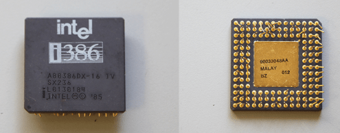
DIP (Dual In-line Package)
The venerable DIP, introduced in 1964, has two parallel rows of through-hole pins projecting from the long edges of a narrow rectangular plastic or ceramic body. Common variations:
- DIP – Dual In-line Package, 2+ pins
- CDIP – Ceramic DIP, widespread until the 1990s
- PDIP or Plastic DIP – Inexpensive molded plastic package
- Narrow DIP – More compact with 0.3” row spacing
DIPs can contain anywhere from 4 to 64 pins. The large, through-hole leads provide robust mechanical connection but limit component density on PCBs. DIPs are still used for moderate complexity ICs like microcontrollers where larger packages are acceptable.
TO – Transistor Outline
Originated for packaging individual transistors, the TO package has evolved into a diverse, expanding family for ICs:
- TO-92 – Small, low-power, plastic, 3-leaded package often used for transistors.
- TO-126 – Larger plastic power package with a metal tab for heatsinking
- TO-220 – Widely used metal can-type package able to dissipate substantial heat
- TO-247 / TO-3P – Large metal package with screw mounting for high power levels
- TO-263 / D2PAK / SOT-223 – Smaller surface-mountable TO style package
TO packages are valued for efficient power dissipation and low cost. However, their size can limit PCB space efficiency versus newer SMT packages.
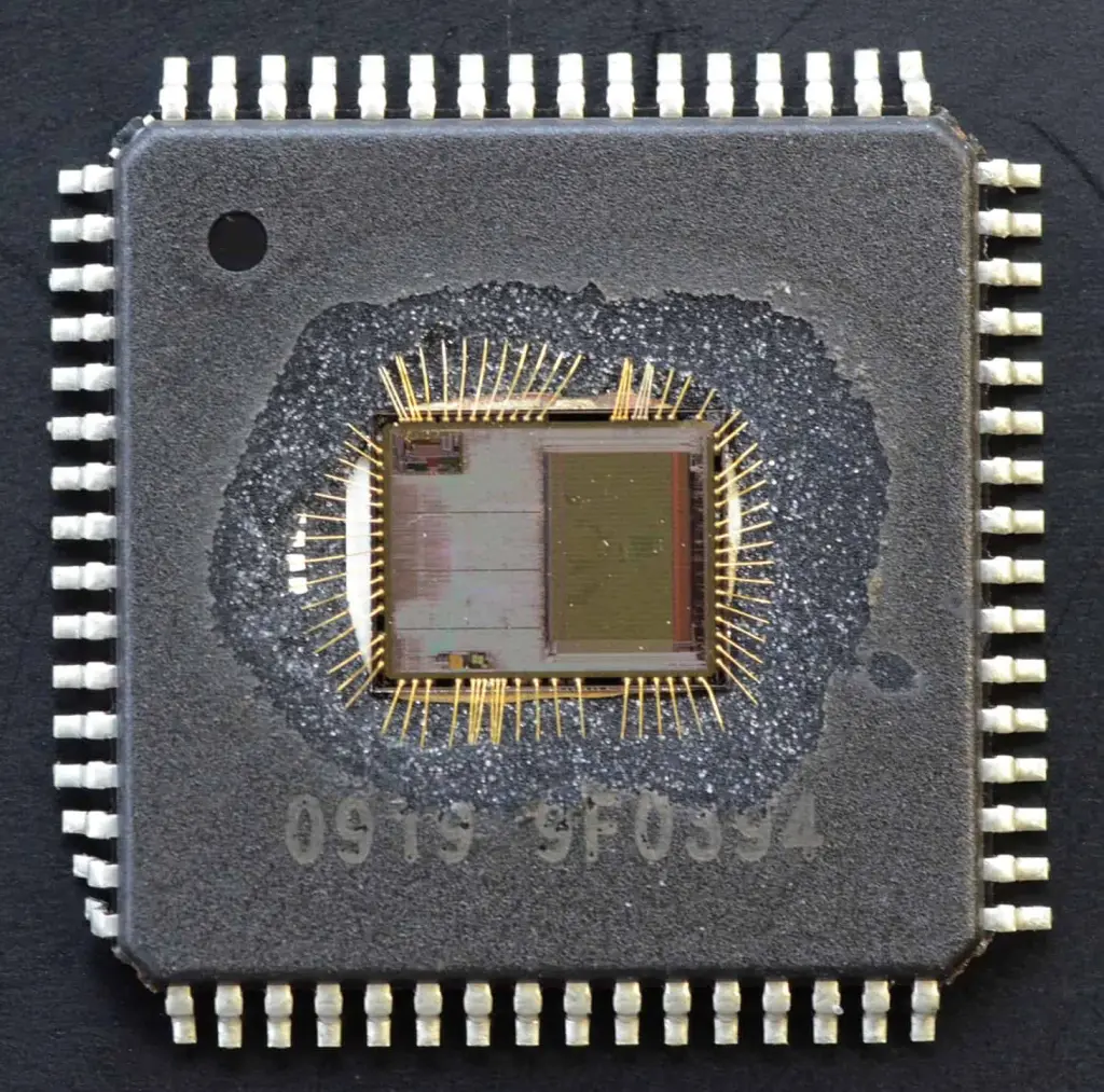
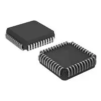
Quad Packages
Quad packages have four rows of through-hole leads extending from the underside of a square plastic or ceramic body. Two popular variations are:
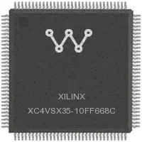
- QFP (Quad Flat Pack) – Four sides of leads in gull wing shape; up to 208 pins
- PQFP (Plastic Quad Flat Pack) – Molded plastic version of QFP with lower cost
With high pin counts in a compact space, QFPs were widely used for microprocessors and ASICs until surface mount packages supplanted them.
While through-hole IC packages dominated early electronics, the need for miniaturization drove adoption of smaller surface mount alternatives.
Surface Mount IC Packages

Surface mount technology (SMT) allows IC packages to be directly attached to the PCB surface rather than plugged into through-holes. This enables smaller package sizes, higher component density, automated assembly and improved reliability. Popular surface mount IC package types include:
SOT – Small Outline Transistor
The SOT family provides small surface mount IC packages suitable for automated assembly. Some key examples:
- SOT-23 – Very small, low profile 3-pin package, typically for transistors
- SOT-223 – Larger plastic SMT power package able to dissipate 5W+ heat
- SOT-89 – Smaller plastic power package often used for regulators
- SOT-143 – Smaller power package with exposed metal tab as heatsink
For low cost, small size and ease of assembly, SOT packages are widely used for power management and analog ICs.
SOIC – Small Outline IC
The SOIC family provides small surface mount IC packages in standard widths similar to common through-hole DIP packages:
- SOIC-8 to SOIC-28 – Narrow versions with 0.05” lead pitch
- SOJC – Wider plastic package with lead spacing up to 0.65”
- SOP – Exposed pad on underside; often used for power devices
SOIC packages range from 1.75mm to 15mm wide. Their modest size, low cost and easy assembly using standard SMT production lines make SOICs popular for analog, logic and communications ICs.
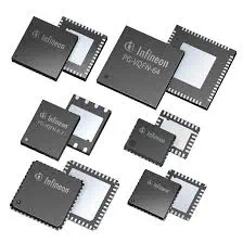
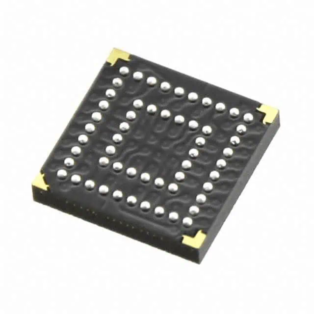
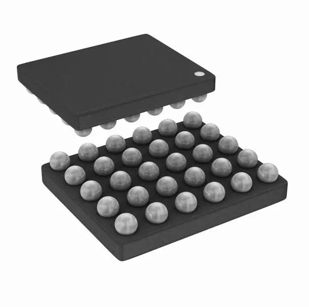
QFN/DFN – Quad/Dual Flat No Leads
QFN and DFN packages have a surface-mounted exposed metal pad on the underside instead of perimeter pins. Some specs:
- QFN – Square footprint, usually pitch 0.4 to 1.0mm
- DFN – Rectangular footprint, similar
- LQFN/QFN-DD – Very compact with 0.4/0.5mm pitch, low profiles
- PowerQFN – Exposed pads for power devices
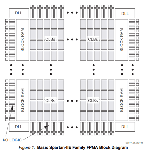
The ‘no leads’ design allows very compact footprint, thin profiles, good thermal and electrical performance. QFNs are often used for processors, ASICs, FPGAs and RF/wireless ICs.
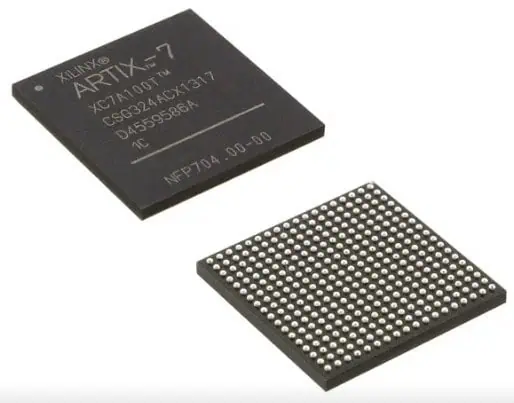
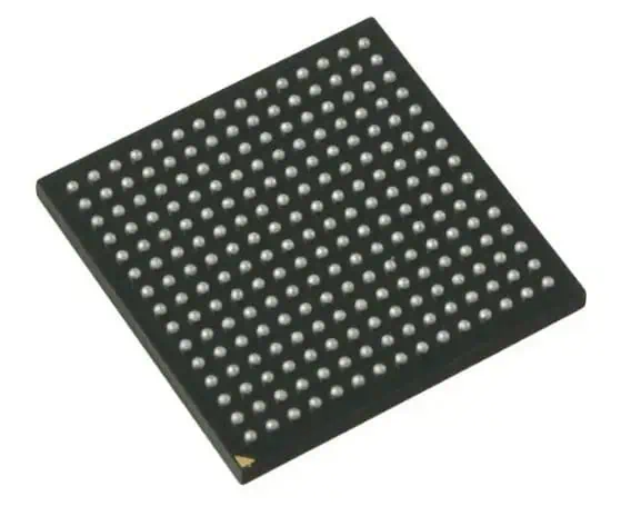
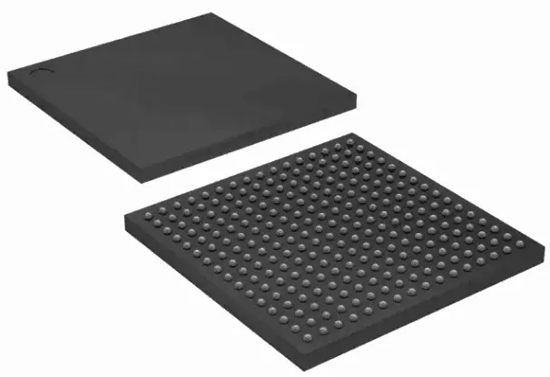
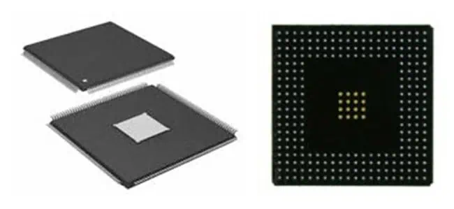
BGA – Ball Grid Array
Instead of pins or leads, BGA packages have an array of solder balls on the underside that connect directly to the PCB surface. Types include:
- PBGA – Plastic ball grid array, lower cost
- CBGA – Ceramic BGA, better thermal and electrical conductivity
- *TBGA *– Tape BGA uses a flexible tape substrate
- μBGA – Micro BGA with very small pitches below 1mm
With their high pin density, BGAs are ideal for complex processors, ASICs, GPUs and chipsets. However, rework and inspection are challenging.
LGA – Land Grid Array
LGAs also have a grid of exposed pads on the underside like a BGA. But there are no solder balls. Instead, spring-loaded clips or sockets make conductive contact with the LGA pads. Benefits include:
- Allows for socketed mounting of ICs
- No soldering avoids PCB substrate damage
- Permits easy replacement and upgrades of ICs
Intel and AMD often use LGAs for their high pin count processors to support socket mounting.
This overview covers the most prevalent IC package configurations used across consumer, industrial, automotive, aerospace and other electronics sectors.
IC Package Materials Overview
IC packages use various encapsulation materials to protect and support the internal silicon die and electrical connections. Common materials include:
Plastic Packages
Plastic is the most widely used IC package material due to its low cost, ease of molding and adequate performance for many applications. Common plastic packaging types:
- Epoxy Molding Compound – Black epoxy resin heavily used for molded packages
- PPS (Polyphenylene Sulfide) – Costlier but higher performance plastic
- LCP (Liquid Crystal Polymer) – Expensive but excellent electrical and moisture protection
- PPA (Polyphthalamide) – High temperature plastic for devices up to 300°C
Plastic packaging is susceptible to moisture intrusion and mechanical stresses. But new materials and construction techniques continue improving plastic package robustness.
Ceramic Packages
Ceramic packages offer higher performance and reliability than plastic for demanding applications, at a premium price. Some ceramic materials include:
- Alumina (Al2O3) – Most common ceramic type; moderately priced
- Aluminum Nitride (AlN) – Excellent thermal conductivity
- Beryllium Oxide (BeO) – Toxic but unmatched thermal performance
- Silicon Carbide (SiC) – Hard, lightweight, high thermal conductivity
Ceramics withstand higher temperatures and have closely matched CTE (coefficient of thermal expansion) to silicon dies. But they still may use plastic encapsulation internally.
Metal Packages
Metal IC packages leverage steel, copper, aluminum alloys to remove heat from high power dies. Examples include:
- Alloy 42 (Fe-Ni-Co) – General purpose, low cost nickel-iron alloy
- Kovar (Fe-Ni-Co) – Well-matched CTE to minimize die stress
- Cu-Mo-Cu – Copper-molybdenum laminate with excellent thermal properties
- AlSiC – Aluminum silicon carbide composite, very high thermal conductivity
Metal packaging is essential for ICs dissipating over several watts of power. The materials are heavier but CTE-matched to silicon.
Hybrid and Multi-Chip Modules
Hybrid microelectronic assemblies combine multiple bare dies and other components in a substrate package providing mechanical stability and electrical interconnection. Benefits include:
- Integration of dies, passives, MEMS, antennas
- Shorter connections yield better electrical performance
- Allows mixed die technologies (Si, GaAs, SiC, etc.)
- Substrate dissipates heat from high power dies
- Reduce size/weight versus separate components
- Lower cost compared to custom IC solutions
MCMs (multi-chip modules) are an important example of hybrid packaging used for miniaturization and high performance assemblies.
Emerging IC Package Materials
Several new IC package materials are emerging including:
- Liquid crystal polymers – Low cost, low loss material for high frequency packages
- Composites like DAP/nSAP – High stiffness and low CTE for large, thin packages
- Photosensitive epoxies – Simplifies embedding bare die in PCBs
- Graphene – Extreme strength and thermal conductivity
IC packaging continues advancing to meet demands for smaller, higher performance and lower cost electronics across all market segments.
IC Package Manufacturing Processes

Producing IC packages requires precision manufacturing and assembly techniques including:
Molding – Used to form plastic encapsulation around the die using transfer or injection molding of epoxy compounds.
Soldering – Solder attach is used to mount the silicon die onto package leadframes or substrates and make electrical interconnects.
Wire bonding – Thin gold, aluminum or copper wires connect the die pads to inner package traces and pins. Both ball and wedge bonding are used.
Plating – Leadframes and traces are plated with nickel, palladium or other metals to enable wire bonding and soldering.
Trimming and forming – Excess leadframe material is trimmed after molding. Leads are bent into shape for through-hole or surface mounting.
Marking – Laser etching or ink printing adds markings with part numbers, logos, pin 1 indicator and other information.
Coating – Anti-corrosion, chemical or hermetic conformal coatings may be applied for additional protection.
Advanced high-precision machinery enables efficient mass production of most common IC package types. But new package designs often require development of custom proprietary processes.
IC Packaging Trends
The relentless trends toward smaller, higher performance, lower cost electronics drive ongoing advances in integrated circuit packaging. Some examples include:
- 2.5D and 3D packaging – Stacking multiple dies in one package enables greater integration in small form factors. High bandwidth interconnects like through-silicon vias (TSVs) connect stacked dies.
- Wafer level chip scale packaging (WLCSP) – Packaging dies at the wafer level prior to singulation reduces materials cost and size. Fan-out WLCSP can provide large solder ball arrays for tight interconnect pitch and integration.
- Embedded die – Dies embedded directly into the PCB substrate or package allow greater component density with enhanced electrical performance.
- Advanced materials – New organic, ceramic and metal materials enhance electrical, thermal and mechanical characteristics.
- Heterogeneous integration – Packaging multiple dissimilar dies and components enables highly integrated modules with optimized performance.
IC package technology must progress to support ongoing improvements in semiconductor die speed, power, functionality and density.
Summary
The IC package provides a critical interface between the fragile silicon die and real-world mounting and operation. Standard package types balance costs, capabilities and manufacturing processes suited to diverse IC applications, from low power signal processing to high current power control. By selecting appropriate package configurations, electrical engineers can fully leverage advancing semiconductor technology across end product segments from consumer IoT to high reliability aerospace electronics.
Frequently Asked Questions
What are the main functions of an IC package?
The key functions of an IC package are:
- Protect die from physical damage or corrosion
- Provide electrical connections via leads/pads
- Remove heat from die during operation
- Allow handling of die and attachment to PCB
- Enable integration into larger electronic system
The package ensures the IC can be utilized in real-world environments.
What are some differences between plastic and ceramic IC packages?
Compared to plastic packages, key advantages of ceramic packages include:
- Withstand much higher temperatures
- Better match of CTE to silicon die
- Increased ruggedness and reliability
- Higher frequency electrical performance
- Improved thermal dissipation
But ceramics cost more than plastics and require careful handling.
What are some key benefits of BGA packages?
Some benefits of ball grid array (BGA) packages are:
- High pin density from grid array
- Overall smaller package size
- Shorter trace lengths boost high speed signal integrity
- Direct surface mounting simplifies PCB assembly
- Fine pitches enable greater interconnect density
- Improved performance for processors, GPUs and FPGAs
The solder ball array facilitates integration of complex ICs.


