Comparison Between Countersink Vs. Counterbore For PCB

Countersink Vs. Counterbore

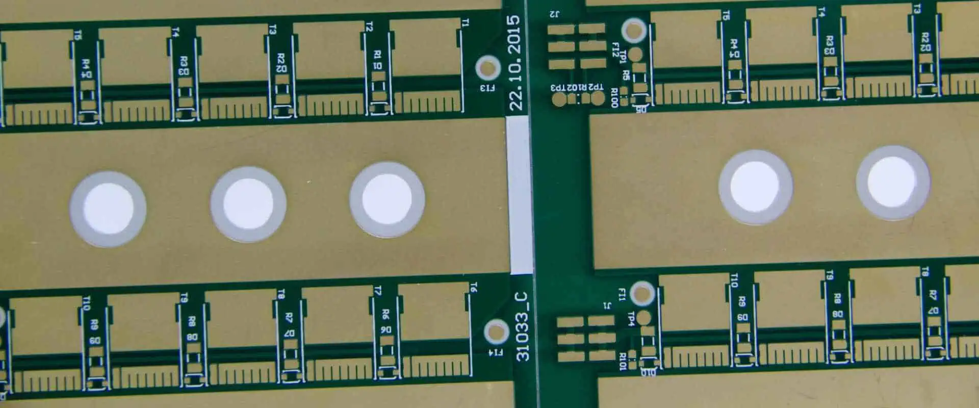
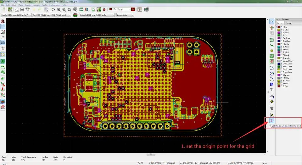
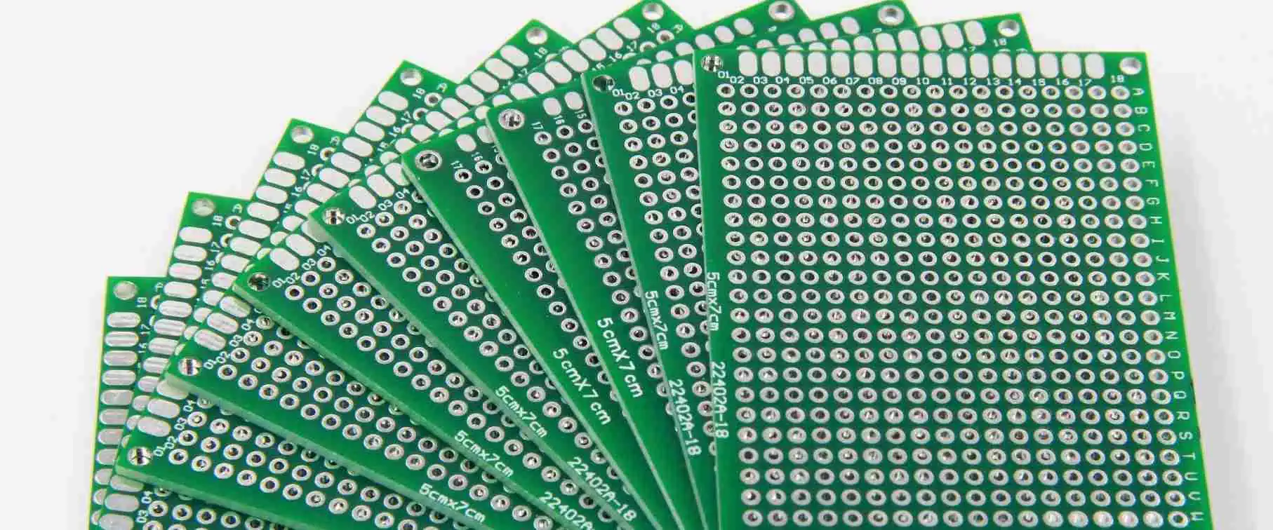
Circuit boards or PCBs have various distinct features which directly affect their functionality and physical structure. You can think about some features normally, like the type of material used in PCB and the number of layers one can have in a board. However, there are a few elements that get less concern. This includes the number of holes, their type, and the drilling process. Particularly, some PCBs need screw holes to meet the board requirement; how these screw holes drill into the board matters here the most. Thus, there are two basic methods of drilling holes in a board. Countersink and Counterbore. Each screw call demands distinct types of holes. The type of screws depicts which method you are going to use for drilling holes. Countersink holes, Counterbore holes, or maybe both. 

What is Countersink for PCB?

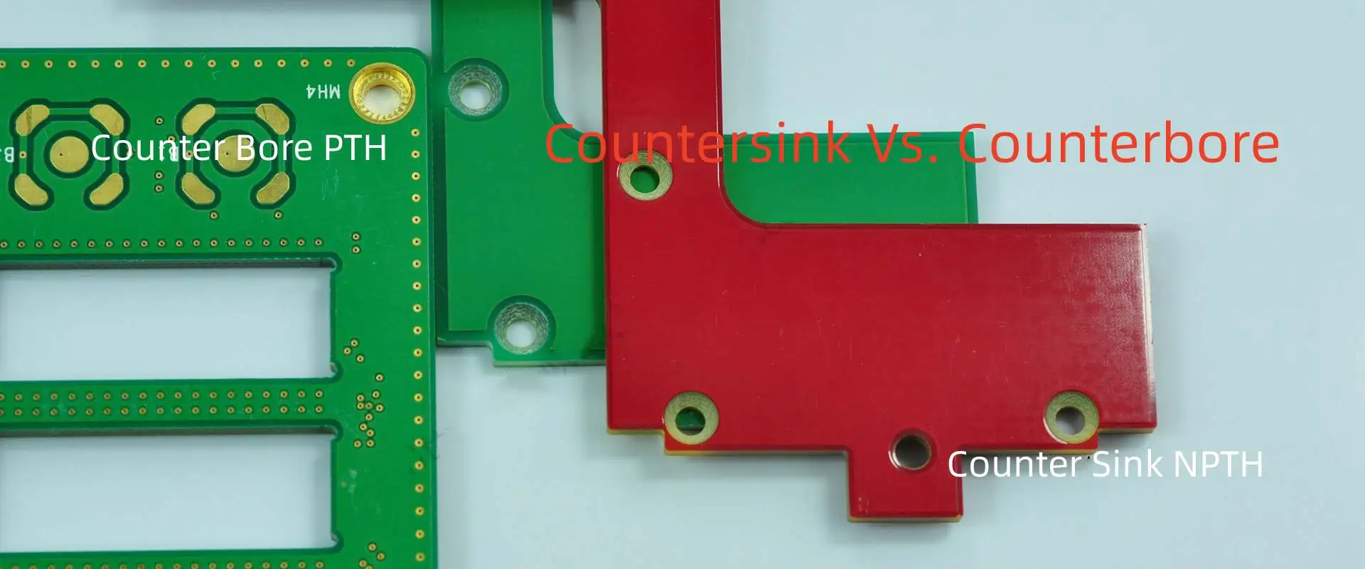
A countersink represents a hole-type drill into a PCB or circuit board. It gives the shape of the cone, which allows the screw or fastener to fit perfectly inside the PCB. Also, these countersink holes have a variety of angle dimensions. The standard countersink hole size ranges the angle between 60, 82, and 90 degrees. 

This does not stop here; you may also drill these countersink holes in different sizes at different angles of 100, 110, and 120 degrees. Moreover, Chamber angles countersink holes with 82, 90, and 100 become popular around the industry.

What is Counterbore for PCB?

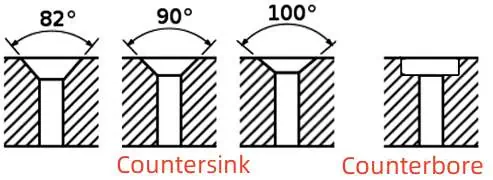
Counterbore is also a type of hole bore in a PCB or Circuit board. It comes in a cylindrical form with a flat surface. This shape allows giving enough space for the hex head or socket head screw. If your board needs these types of screws for fastening, then a counterbore hole is what you need. 

Counterbore holes can only drill at one angle, zero degrees which also needs to keep hole efficiency in mind. This also means that one can only use counterbore holes for solely one purpose. Whereas, unlike counterbore holes, countersink holes utilize for different applications with a variety of angles.

Similarities And Differences Between Countersink Vs. Counterbore For PCB

Countersinking is a process of drilling countersink holes in a PCB. Countersink holes come in a variety of sizes with different angles. The standard angle size includes 90, 82, and 60 degrees, while the less popular size includes 120, 110, and 100 degrees. Well, the most well-known angle sizes include 100, 90, and 82. Whereas, unlike countersink holes, the counterbore hole only has one standard angle size, zero degrees. It acts and affects in the same manner, just like a countersink hole.

You must work efficiently while drilling holes in the wooden surface boards. If by any chance you forget to drill the countersink hole, but later on, force the screw or fastener into a wooden surface. This not only affects the strength and stability of the wood but also affects its look and makes it miserable. This is because the fibers of wood get damaged and cracked easily. However, drilling a counterbore on the surface of wood seems like a good idea as it does not need accuracy and precision in the sizes of angles. 

Moreover, all counterbore holes require a socket or flat bottom screw that can suit the surface easily. Counterbores typically serve a sole purpose, whereas countersinks serve various purposes due to a wide variety of angle sizes. 

A counterbore hole looks for a tiny coaxial hole opening, whereas a countersink hole looks like a conical shape. This comes in handy when you donโ€™t need a screw or fixtureโ€™s head into the surface of HDI. Furthermore, countersink holes can also have various styles and shapes due to their various angles. But countersink holes give the same depth to all the screws.

Countersink Vs. Counterbore Symbol 

In design and drawing, the symbol represents the actual technique or material. These symbols provide a space for specification tolerance and dimensional consistency. However, writing symbols or signs of a quantity or material is an easier and faster way than spelling out the complete name. It not only breaks the drawing standards but also makes the work messy. 

Symbols indicated the standard protocols in mathematics, design, and drawing. In various projects like a blueprint of a house or drawing, symbols help in conveying information faster. That is why both counterbore and countersink holes have symbols. It mostly writes along with the symbol of diameter and has a figure value.

Symbol of Countersink 

The symbol of the countersink hole indicates the alphabet V. The countersunk hole resembles the alphabet V when you look at it from a side posture. 

Symbol of Counterbore Symbol 

The counterbore hole symbol resembles an unfinished square with a top opening. The symbol comes by taking a look at both counterbore and countersink holes. Both symbols come in handy in the designs of drilling. The emblem of diameter represents the deepness and wideness of a hole in a board. A designer depicts these values based on data provided in such designs. The symbol of counterbore defines the operation of counterboring, while the symbol of countersink defines the fastening operation of countersinking.ย 

Countersink Vs. Counterbore Drill Bits

FULL PCB MANUFACTURING Quote

You can drill many holes with the drill bit. Based on the material thickness and the desired diameter. Both the countersink and counterbore use hole drills to commence the process. At the same time, drill bits are used to create countersink and counterbore holes inside a PCB or the material. Both drill bit holes use a distinct type of material for manufacturing. Basically, their main goal is to fit the fastener or the screw into the workpiece of the washer. 

One cannot ignore the axis and the length of the crew or the fastener in the counterbore or countersink hole. Different materials are utilized for fabrication due to the cavity distinction of both types of holes. A type of cylindrical hole bores inside the surface of the material for counterboring. This hole contains a small diameter at the bottom and a large one at the top. 

The main goal of the hole is to hold both surfaces firmly so that they wonโ€™t separate from each other. The head of the fastener goes into the larger edge while the shaft goes into the smaller side. Therefore, drill bits of countersink come in a variety of sizes and styles to adjust various projects at different angles. There are four basic types of drill bits for the countersink. This includes flip-style, rocker pro, cross-hole, and fluted bits countersink.

When to use Countersink Drill Bits?

Make sure to match the size of the drill to the screw while using drill bits of countersink. A too-large countersink hole swallows the fastener or screw head. At the same time, a tiny hole doesn’t allow the screw head to fit into the board. This leads to an unfit mount. However, a question arises, what if you put the screw inside the hole forcefully? Undoubtedly, if you try to drive the screw forcefully into the hole, it may damage the material surrounding it. This happens with both wooden and HDI surfaces. 

Same as if the hole is too wide, the screw will get shallow, while if the hole is too shallow, it will not allow the screw to fit inside the surface. Therefore, measurements play an essential role in the whole drilling process. To get perfect measurements, adjust the setting of the countersink. The setting includes the size of the countersink, the depth of the drill bit, and the stop location of the center. However, it’s still recommended to first practice these measurements over the piece of scrap material. So that you adjust the setting beforehand if something goes wrong. 

Furthermore, never drill faster to prevent chattering. As it leads to uneven design on the surface of the material. Also, it does not allow the fastener to fit, which makes your board or material messy and unusable.

Using Countersink & Counterbore In PCB

With an understanding of the basics of both countersink and counterbore holes, let’s dive into their usage in the PCB. However, both types of holes are mainly used in wooden and metal surfaces, but they will also go well for a PCB. PCB also has holes that use drilling techniques, and each hole in the PCB counts and matters. Some use screw holes. It helps in attaching the Device with a PCB. The type of screws you want to drill determines the types of holes you will use in the PCB. A counterbore or a countersink hole.

ยท Limited Space & Mounting Security 

The Countersink hole plays a vital role in your PCB having compact or less space. It helps in adding additional features like enhancing the flexibility of the device. This conical-shaped countersink hole is a typical type of flat-head screw that requires greater precision and accuracy as compared to counterbore holes. Once the fastener or screw fits into the board, later it becomes easy to adjust the circuit inside the device. The device may include a watch or a smartphone. A counterbore is easy to drill. However, it does not fall into an ideal choice for most PCBs.ย 

Countersink holes do not affect the surface of the board and keep it smooth if drilled correctly. Also, it does not disturb the arrangement of a PCB. However, counterbore holes come in if you need secure mounting in a PCB beside a smoother surface or converse space. These holes provide enough space to fit the socket fixture. Therefore, these holes and screws make stronger connections. But if you need to conserve surface, then use countersink holes. 

Applications of Countersink Vs. Counterbore

A PCB use is mounted through a screw into a hole. Therefore, both counterbore and countersink holes can use for stronger and safer installation. Engineers use automated equipment manually to commence this process. A counterbore hole is drilled with a grub fastener or screw. This gives an ideal base for a screw to fit perfectly inside the hole.

Countersink Vs. Counterbore – Uses

In PCBs, countersink holes provide perfect fitting and smooth installation into compact devices. PCB countersink mostly includes small wearables and smartphones. A counterbore hole provides a tight fit to a screw in a cylindrical manner. Due to its flat bottom, it uses a socket cap-type screw. This socket screw contains a hex head which needs safe and secure mounting in a PCB. The application of this type of PCB includes electronic devices, like washers which need secure and tight fitting.ย 

Dimensioning Techniques of Countersink Vs. Counterbore 

Aluminum PCB Countersink hole

Dimensioning plays a vital role in the design process. This allows the designer to convert the drawing into real life. Dimensioning mainly depicts the type, size, and material texture used during fabrication and construction. Dimensioning methods express counterbore and countersink holes in a chart or a design through various dimension abbreviations and symbols. These depict the type of surface and provide zero restriction over the fabrication method. However, these dimensions typically refer to the note and are followed by hole size. 

How To Dimension A Countersink & A Counterbore?

The angular edges in a countersink process go through the recession to provide a fit to flathead fixtures head which can be rivets, screws, or bolts. During drawing, it provides the diameter of the surface, its angle, drilled hole, its diameter, rise, and depth. The cylindrical part and flat bottom of a counterbore allow the head of the fastener to fit in a recessed part.

During drawing, it provides the depth, diameter, and radius of the corner. In some scenarios, the remaining shaft thickness can also be dimensioned in the center. Both countersink and counterbore holes dimension in a polar and rectangular coordinate form.

Conclusion 

Both countersink and counterbore holes use different types of screws in distinct types of materials. However, both work in a similar manner in a PCB. A countersink makes a cone-shaped hole, whereas a counterbore makes a cylindrical shape hole. This article briefly explains the definition, similarities, differences, and working principles of both countersink and counterbore holes. 

The screw types that fit in countersink and counterbore holes refer as countersinks and counterbore. Both use different types of drill bits for distinct types of materials. Also, this article shows how and when to use these drill bits in a PCB according to their usage and application.

Moreover, it also describes its symbols, different types of dimensioning techniques, and their applications. 

A Look at the Protective Capabilities of Parylene Coating

The surfaces of Printed Circuit Boards (PCBs) are protected with parylene coating because of the excellent protective features of the coating. As a conformal coating process, it is one of the ways you can keep the circuit board components safer.

In this article, we let you into some of the protective capabilities of the parylene c coating process.

What is PCB Coating?

Let us start by understanding the meaning of coating. When a PCB is said to be โ€œcoated,โ€ it means that it has had some thin, protective materials applied to the surface. These materials are responsible for preventing a direct contact between the PCB components and the environment. To this end, important parts like the exposed metal, component leads and solder joints are protected with the help of the coating.

YouTube video

What is Parylene Coating?

It is one of the different types of coating options you can explore to protect the circuit boardโ€™s components.

Parylene coating is defined as a conformal coating comprising of a thin film coating technology, which is used to improve the capabilities of devices. You can also use parylene coating to integrate excellent moisture and chemical protection on these devices.

Step-by-Step Parylene Coating Process

Parylene Coating PCB

The steps to coating a device or a Printed Circuit Board (PCB) with the parylene coating is divided into four processes.

Each of these processes are important and when followed to the latter; helps to bolster the device or PCB componentโ€™s protection.

1. Adhesion Process

This is the initial process and it entails the solidification of the bond between the underlying substrate and the parylene.

2. The Masking Process

The creation of a mask is for two purposes. The first is to demarcate or create a space between the protected areas on the PCB and the other areas that were not coated. The second purpose is to prevent the extension of the parylene to the areas or surfaces that needed to be kept free of the coating.

3. The Coating Process

The main coating process starts after the mask has been applied. It is preceded by the placement of the PCB components or parts on a fixture. This fixture is then loaded into the vacuum deposition chamber.

The following are some of the techniques used in the parylene coating process:

  • The Chemical Vapor Deposition (CVD) process is used for the coating. The deposition method includes the vaporization of the parts up to 150-degree Celsius, followed by the pyrolyzed process of up to 650-degree Celsius. It is to be followed by the use of up to 22-degree Celsius of vapor-deposition into the parts.
  • Room temperature must be used during the coating process.
  • A specialized vacuum deposition equipment should be used too.

4. Post-Coating Processes

This refers to the different implementations to be made after the PCB components have been coated.

The post-coating processes include, but are not limited to:

  • Parylene Coating Thickness Measurement: the thickness of the parylene films is to be measured. The measurement process requires the direct placement of spectral reflectance on the PCB parts.
  • Remove the Mask: when the parylene coating thicknessโ€™ measurement is completed, you can then remove the mask. Take care not to fracture the coatingโ€™s fixture while at it.
  • Inspection: after the parylene coating removal, the PCB parts would then be inspected. The inspection is carried out for a wide range of reasons, such as validating the presence of the quality attributes and the meeting up with the clientโ€™s requirements. Some of the quality attributes specify the adhesion-testing, coating thickness and area of coverage.
  • Product Labeling: the completion of the microscopic-inspection of the components ushers-in the packaging of the parts. Proper labeling, as per the clientโ€™s requirements must be followed.
  • Shipping: we can help ship your parylene-coated PCBs in real-time. Depending on the volume or quantity, you should expect to have the parts in a couple of days.

Parylene Deposition Method

FULL PCB MANUFACTURING Quote

There are a couple of things you need to know about how the deposition of parylene conformal coating is done.

1. Temperature Consideration

The deposition process is done at ambient temperature. For this purpose, a specialized vacuum deposition equipment or specialized vacuum system is used.

2. Molecular Level Basis

The deposition process takes place at a molecular level, which signifies the deposition or placement of molecules on each of the parts placed in the vacuum chamber.

The molecular deposition process is also significant for the following reasons:

  • It leads to the creation of an even conformal coating that covers the sharp points, grooves, gaps and crevices on the parts.
  • The molecular deposition process also aids the excellent control of the thickness.
  • It also bolsters the growth of the films, a molecule at a time.

3. The Parylene Deposition Process

The steps involved in placing the molecules via the deposition include:

  • Partsโ€™ Fixture: the parts are fixed into a vacuum coating chamber.
  • Dimer Heating: โ€œdimerโ€ refers to the solid, granular/powdery material, which is used for the process. It is placed inside the vaporizer, and heated at a higher temperature. The process leads to the losing of the โ€œdouble-molecule structure,โ€ and the outcome is the reduction to a โ€œsingle molecule vapor.โ€ The heating process leads to the turning of the dimer from the solid state to a dimeric gas.
  • Vapor Polymerization: the gas is then pyrolized to cleave the dimer to its โ€œmonomeric form.โ€ It is important to mention that the process typically requires the flow of the dimer into the pyrolysis furnace, where additional heat is added to the dimer. This is what leads to the conversion to monomer vapor.
  • Gas Deposition: it is then time to deposit the gas or monomer gas onto the PCB partsโ€™ surface. It is first moved into a room-temperature deposition chamber, where the vapor polymerizes onto the substrate. The deposition is in the form of thin, transparent and uniform polymer film.

Types of Parylene Coating

Up to four (4) different types are available for parylene coating PCB. They include:

1. Parylene C

It is a type of parylene coating comprising of a combination of carbon and hydrogen. This is why it features both the dielectric and barrier properties.

The composition of an atom of chlorine in place of one hydrogen atom per molecule is the reason why it features low permeability. Some of the characteristics are:

  • Higher moisture resistance.
  • Support for thicker layer application.
  • It offers better protection from corrosive gases and chemicals.
  • Parylene C has cost and processing advantages, especially due to the less machine time.

2. Parylene D

Although it is much like Parylene C, the Parylene D coating type use two atoms of chlorine in place of two hydrogen atoms. It also features a slightly higher temperature tolerance and up to 100-degree Celsius of assembly protection.

The benefits of choosing it include:

  • It holds high when exposed to higher temperatures.
  • It features improved electrical properties and physical strength characteristics.

3. Parylene F

This type of parylene coating comes in handy for the applications where the Parylene D donโ€™t hold up. For example, it is more resistant to Ultraviolet (UV) light exposure than the Parylene D.

The properties include but are not limited to:

  • The formation of four (4) fluorine atoms on the aromatic carbons.
  • It has good crevice penetration.
  • It is capable of operating at higher temperatures.

Note: it is better to use the Parylene F coating for the medical device applications, especially those requiring higher temperatures. On the flipside, the raw materials are quite expensive and it has a slower deposition time.

4. Parylene N

As one of the most popular parylene coating types, Parylene N has a linear structure and has a carbon-hydrogen combination on each of the molecules. It is often considered to be the basic structure of the Parylene coating types, due to the following properties:

  • Low dielectric constant that doesnโ€™t change due to frequency discrepancies or changes.
  • During the deposition process, it becomes more molecular-active.
  • Low dissipation factor.
  • The increased crevice penetration prepares the way for the coatingโ€™s penetration into smaller openings and tubes.
  • It is typically used with applications or devices requiring higher frequencies.
  • The melting point is up to 788หšF or 420-degree Celsius.
  • It has a higher dielectric strength.

Parylene Coating vs. Non-Conformal Coating

PCB Assembly conformal coating

There are two (2) major coating processes for Printed Circuit Boards (PCBs). These are the conformal and the non-conformal processes.

For the conformal, which is what the parylene coating process is all about, it entails the application of a non-conductive material on a thin coating over the PCBโ€™s surface. Some of the covered surfaces are the components, substrate, solder joints and exposed metal.

On the other hand, the non-conformal coating process requires a thicker coating procedure that covers the entirety of the board.

Thus, the difference between the two is that the parylene coating process covers only specific surfaces, while the non-conformal coating procedure covers most of the boardโ€™s surfaces.

Conclusion: Work with Parylene Coating Companies

The process of applying a parylene coating on the boardโ€™s surface requires precision and the technical know-how. This is why working with RayPCB is a step in the right direction. We are one of the few companies you can trust on to apply the thin conductive material all over the required surfaces on your PCB, while making sure that the material conforms to the board areaโ€™s contours.

Contact us today with your requirements to get started.

Understanding the Surface Mount Package

SMD package

Electronic engineers integrate various types of electronic components called surface-mount devices in their everyday work. Electronic components are a crucial part of electronic devices. There are different types of SMD packages. SMD packages are a certain kind of equipment or component contained within a single packaging. These packages function as component groups that make it much easier to identify their physical qualities. The physical size and characteristics of SMD packages define them.

This article aims to provide the engineers interested in sourcing electronic components in their various sectors well-detailed information about surface mount package sizes, types, and applicable standards.

YouTube video

What Does Surface Mount Package Mean?

SMT components, which use surface mount technology, are available in various types of packaging. There has been reduction in sizes of different packages due to the improvement of surface mount technology. A range of other SMT packages are also available for the integrated circuits, however, this depends on the level of interconnection needed, the technology that is being employed, and a number of other considerations.

There is a wide selection of different SMD packages. A special circuit board with a matching copper design on which they are soldered is usually needed to work with surface-mount boxes. Since there are a various SMD packages, a customer may choose one of these packages according to how convenient an electrical component is for them.

Surface Mount Package Requirements

Most SMT component sizes adhere to the industry standards, of which a large percentage is the JEDEC requirements, to ensure some level of standardization.

Certainly, various SMT packages were utilized for various component types, however the existence of standards makes tasks like PCB design much simpler. Moreover, production is made easier and faster by using packages of standardized sizes. Since pick and place machines may integrate standard feed for SMT components, this will likely streamline the process and as well reduce costs.

Surface Mount Packages Categories

There are standardized packaging for each of the component types, and the various SMT packages may be divided into those categories.

Passive rectangular component

This SMT component comprises capacitors and resistors, which amounts for the majority of the total number of parts utilized. Since technology has made it possible to produce and utilize smaller components, various sizes have been minimized.

Semiconductor SMD package

For semiconductors like diodes, transistors, as well as integrated circuits, you can integrate various surface mount packaging. The broad variance in the needed amount of interconnection is the cause of the huge diversity of SMT packages used for the integrated circuits. Some important packages are listed below.

Packages for transistors and diodes

These packages are frequently integrated for SMD diodes and transistors.  Diodes usually feature two electrodes; the package having three electrodes makes it feasible and easy to choose the orientation accurately.

SMD Diode on the Printed Circuit

Although there are other SMT transistor as well as diode packages available, we will be discussing the well-known ones.

SOT-23 – The Small Outline Transistors: This SMT package contains three terminals strictly for the transistor diode. Its dimensions are 3 mm by 1.75 mm by 1.3 mm.

SOT-223 – The Small Outline Transistors: This package can be utilized for applications where higher power is a concern. Its dimensions are 6.7 mm by 3.7 mm by 1.8 mm.

SMD Packages for Integrated Circuits

SMD ICs can be packaged in a variety of ways. Despite the wide variety, each of them has its own use. Small Outline Integrated Circuits: This SMD package includes gull wing lead that features a 1.27 mm pin spacing as well as the dual in line layout.

Small Outline Packaging

There are many iterations of this particular SMD package. These include:

  • TSOP, or Thin Small Outline Packaging, is a thinner SMD package than the small outline integrated circuit SOIC with 0.5 mm pin spacing.
  • Shrink Small Outline Packaging (SSOP) – This features a pin spacing of 0.635 mm.
  • TSSOP – This is the Thin Shrink Small Outline Packages:
  • Quarter-sized Small Outline Packaging: The pin spacing is 0.635 mm.

Very Small Outline Packaging (VSOP): This is a smaller version of the QSOP and features pin spacing of 0.65, 0.5, or 0.4 mm.

There is a general term that represents a flat container for IC. This term is known as  QFP, or quad flat pack, is a general term for a flat container used for ICs. This is a list of the various variations.  Low profile quad flat pack also known as LQFP has pins across all its four sides. Its height is 1.4 mm, although the spacing of this pin may vary based on the integrated circuit.

PQFP – The Plastic Quad Flat Packs: The square plastic packaging has an equal number of pins in the shape of gull wings on every side. Usually with at least 44 pins and a narrow spacing.

CQFP – The Ceramic Quad Flat Packs: This is the ceramic variant of a PQFP.

TQFP: This is a smaller variant of the PQFP is the TQFP, or Thin Quad Flat Packs.

BGA: The ball grid array is an integrated circuit package which enables electrical contact with a printed circuit board through pads that are beneath the package. This terminology was coined from the fact that the pads look like solder balls before the process of soldering.

PCB manufacturers integrating these package pads may place them beneath package; this offers solutions to some of the problems associated with the extremely thin leads required for quad flat packages. When it comes to BGAs, the spacing of the ball is exactly 1.27 mm.

Applications of Surface Mount package

Most printed circuit board design manufactured in various quantities integrates surface mount packages. There could be a level of uniformity despite having a wide array of diverse packages. This level of uniformity can still be achieved. In any case, this usually results from the variation in the performance and functioning of these components.

SMD or SMT?

People always confuse SMT with SMD. They interchange these two terminologies. However, there is a difference between the two. So, what is the difference  between SMD and SMT? The main difference between surface mount technology and surface mount device is  that SMD is an electronic component usually installed on a printed circuit board. On the other hand,  SMT is a technique in which these electronic components are mounted on the bare circuit board. A bare circuit board has no surface mount device on it.  

The SMD device

One thing you need to know is that lead-based components differ from the build-up components. The surface mount device (SMD) parts are designed in such a way that they are soldered to a board instead of  linking between two locations.

In conventional leaded components, the leads donโ€™t always go via the holes in the circuit board. There are different kinds of  components. Therefore, there are various ways of packaging these components. Among the packaging styles, you can distinguish three different broad types. These types of SMD component packages are passive components, diodes and transistors, and also integrated circuits. We are discussing these types of SMD below:

Passive SMDs

The passive SMDs require the use of various packaging options. However, it should be noted that most passive SMDs are SMD capacitors or SMD resistors. In this case, the package sizes will be extremely defined. Crystals, coils, and other components commonly have more unique needs. Therefore, these components always come with their own containers.

Furthermore, capacitors and resistors are available in a wide range of package sizes. These resistors or capacitors have the identifiers 0201, 0402, 0603, 0805, 1206, and 1812. These measurements are in centimeters and are indicated by the numerals. This means that the 1206 has a dimension of 12 by 6 hundredths of the inch. The bigger sizes, like 1206 and 1812, were among the first utilized.

Diodes and Transistors

Manufacturers make use of small plastic packages to package SMD transistors and SMD diodes. The cables are bent to ensure they maintain a contact with the circuit board when they are removed from the box are used to make the connections.

Integrated Circuits

When it comes to packaging ICs, various types of packaging is used. A particular package is usually integrated. However, this depends on the level of interconnectivity needed. While certain circuit boards, like basic logic chips, might just require about 16 or 14 pins.  VLSI processors and related chips, may require a minimum of 200 pins. There are many distinct packages available due to the huge range of needs.

Small outline integrated circuit can be used to package smaller chips. These are essentially the SMT versions of the popular Dual In Line (DIL) packaging utilized by the popular 74 series logical chips. Also, there are other smaller variants that can be used. This includes the thin Small Outline Packages and Shrink Small Outline Packages.

Size of Surface Mount Packages

What is a 0201 SMD?

Devices with a surface mount include resistors, transistors, capacitors, and more. It is important to note that SMD component packages are usually available in various sizes. You will find these sizes marked on these SMD components.  This helps in distinguishing the sizes from one another. This 0201 SMD packages also has dimensions of 0.024″ by 0.012″, or 0.6 by 0.3 mm.

This 0201 SMD is specifically designed to increase dependability in applications where spacing is a top priority. Portable electronics like tablets and cellphones are one of these use cases. It should be noted that careful handling is required when assembling these 0201 SMD parts.

Understanding the Imperial and Metric codes for the 0201 SMD

There are two distinct ways to express SMD component sizes. Finding these methods might be quite difficult for component purchasers.

It can be confusing to differentiate how imperial or metric codes are used. However, these codes are quite easy to understand if you pay attention. The numerical code represents the size of the components.

Also, you can express imperial code in inches. For example, the 0201 imperial codes indicates a component is 0.02 x 0.01 inches in size. Metric codes are measured in millimeters. For instance, using 0201 SMD metric codes denotes a component which has a size of 0.2 x 0.1 mm.

Surface – Mounted Discrete Resistors

The thin film and the thick film are the two types of surface mount resistor.

The Thick Film Surface – mounted Resistors: Rather than deposit the resistive films on circular cores like axial resistors, the SMD is made by the screening ruthenium dioxide-based paste and perhaps a comparable substance on high-purity, flat alumina substrate surfaces.

Thin Film Resistors: They are built on the ceramic substrates with a protective covering, sometimes known as the glass coating, and have silver coated as thick film pastes on a ceramic substrate present on these terminators.

This resistor seems to have a resistive layer having protective coating on one side as well as white base layer on the other. Hence it is easy to differentiate capacitors and resistors based on their external appearance.

Ceramic Capacitors for Surface Mount

When you are in need of an SMD packaging ideal for high-frequency circuits,  you need to consider the surface mount capacitor. You can position this below the container somewhat on the opposite side of the circuit board. This application SMT capacitors serve as decoupling applications including frequency control.

LCCC – Leadless Ceramic Chip Carriers

The castellation terminations on the LCCC are groove-shaped, gold-plated terminations which provide shorter signal routes and more operating frequencies.

However, it is possible to categorize the leadless ceramic chip carriers in many families based on its specific package pitch. 50 mil leaded ceramic chip carrier groups are very popular. However, there are other families which 20, 25, and 40 mil.

Conclusion

Over the past years, there has been a huge development on the production of printed circuit boards. The sizes of these boards have been reduced due to the introduction of integrated circuits. These tiny boards are capable of holding several components. However, it is of utmost importance to ensure components and wires on the PCB are well installed. This is because improper installation can result in short circuits and other problems. Therefore, you need to pay precise attention when choosing surface mount devices and components.

Ultimate Guide to XC6SLX9-2TQG144C FPGAโ€™s Application in Telecommunication And Medical Field

wholesale Xilinx FPGA

The XC6SLX9-2TQG144C is a powerful gizmo FPGA. It is useful for a wide range of applications. FPGA stands for Field-Programmable Gate Array, and it is a type of semiconductor device. 

This device is programmable to perform any type of digital function. The XC6SLX9-2TQG144C is one of the most popular FPGAs in the market because it is useful in a variety of applications.

In this article, we will explore the uses of the XC6SLX9-2TQG144C FPGA in detail. Before getting into applications, let’s have a look at basic features.

Features of the XC6SLX9-2TQG144C FPGA

The XC6SLX9-2TQG144C FPGA is a high-performance device that offers a wide range of features and capabilities. Some of its key features include:

  • Like any other FPGA, the XC6SLX9-2TQG144C FPGA is designed to consume less power. That’s why it is ideal for battery-powered devices. Furthermore, it does not consume more voltage.
  • This FPGA shows high-Speed Performance. That’s why it is capable of processing data at high speeds. In addition, it is ideal for real-time processing applications.
  • The XC6SLX9-2TQG144C FPGA has a large capacity, that’s why it can handle complex applications. Similarly, it can perform multiple functions altogether. He FPGA is able to be reprogrammed and reconfigured. That’s why it is ideal for performing a wide range of functions. In addition, it is an ideal tool for prototyping and development.

Applications of the XC6SLX9-2TQG144C FPGA

The XC6SLX9-2TQG144C FPGA can be used in a variety of applications but in telecommunication, it has a variety of uses. Similarly, in the medical field, it has multiple uses.

1. Application In The Telecommunication Industry

The realm of telecommunications is presently undergoing rapid transformation with the advent of novel technologies and an escalating demand for faster and more efficient data transfer. To cater to such exigencies, telecommunications corporations are employing sophisticated hardware and software technologies, among which one such technology that has garnered significant attention is the use of Field Programmable Gate Arrays (FPGAs). Of noteworthy mention is the XC6SLX9-2TQG144C FPGA, which is a highly potent device that offers a wide array of applications in the telecommunications industry.

 The XC6SLX9-2TQG144C FPGA has various uses in telecommunications. It can process and transmit data at high speeds. In addition, it has applications in wireless devices to enhance Performance. Similarly, it can improve the range of wireless signals. In addition, its low power consumption and high processing speed make it ideal for many other telecommunication devices.

The XC6SLX9-2TQG144C FPGA has applications in baseband processing. It involves signal modulation and demodulation. Similarly, it involves channel coding and other operations necessary for wireless communication.

XC6SLX9-2TQG144C FPGA is also utilized for network infrastructure. For example, high-speed data transfer is essential for routers and switches. The XC6SLX9-2TQG144C FPGA is able to perform packet processing and other functions to ensure efficient data transfer. Data centers require high-speed data transfer for professional data processing. The XC6SLX9-2TQG144C FPGA has applications in the acceleration of algorithms and encryption. Similarly, it can do data compression also. That’s why XC6SLX9-2TQG144C FPGA has multiple applications in the telecommunication field.

2. Robotics For More Precise Industrial Control

The XC6SLX9-2TQG144C FPGA is part of many industrial control systems to monitor and control processes. Because it provides more precision and control, similarly, it is also part of robotics to improve their Performance and precision.

3. Medical Devices and Process Equipment

Following are some possible uses of XC6SLX9-2TQG144C FPGA in the medical field.

The XC6SLX9-2TQG144C FPGA is a part of many medical devices to route and analyze patient data. It is also used in medical imaging equipment to enhance the quality of images. XC6SLX9-2TQG144C FPGA FPGAs are used in medical imaging applications.  For example, X-rays, CT scans, and MRI machines have FPGAs. These machines require high-speed processing of large amounts of data, so FPGAs serve best for this purpose. All modern Patient Monitoring systems have XC6SLX9-2TQG144C FPGA: FPGAs. These systems perform real-time processing of physiological signals such as ECG, EEG, and blood pressure. 

Such modern medical equipment uses it for detection of abnormalities and timely intervention.

ย FPGAs provide more control over medical equipment. Such equipment includes infusion pumps, ventilators, and surgical robots. These devices require precise timing and synchronization, and only XC6SLX9-2TQG144C FPGA can provide it. Moreover, XC6SLX9-2TQG144C FPGA is a part of much modern medical equipment that is helpful for research. Such equipment shows better results in it comes to signal processing and imaging. These FPGAs are helpful in the development of new medical technologies and treatments.

Benefits of using the XC6SLX9-2TQG144C FPGA

FULL PCB MANUFACTURING Quote

The XC6SLX9-2TQG144C FPGA offers a number of benefits, including:

  • The XC6SLX9-2TQG144C FPGA helps to perform complex operations at high speeds. As a result, it can improve the performance of your applications. It is one of the greatest perks of FPGA.
  • XC6SLX9-2TQG144C FPGA offers great flexibility. You can reprogram and reconfigure these FPGAs to perform a wide range of functions. It is an ideal tool for prototyping and development.
  • XC6SLX9-2TQG144C The FPGA reduces the cost of development and production. You don’t need to buy multiple chips with a single device. FPGA serves the purpose best.
  • Customization is the uniqueness of any FPGA. The XC6SLX9-2TQG144C FPGA is easy to customize. It is helpful to meet the specific needs of your applications. It can improve their Performance and functionality.

 Wrapping up

The XC6SLX9-2TQG144C FPGA is an extraordinarily versatile and potent tool, serving various industries, such as telecommunications and medicine. Its sophisticated attributes, including high-speed data processing, energy efficiency, and effortless programmability, make it appealing for complex jobs like image and signal processing. Regarding the telecommunications industry, the XC6SLX9-2TQG144C FPGA can operate in numerous areas, including network processing, data encryption/decryption, and wireless communication. The tool’s ability to manage rapid data streams with minimal latency and extensive bandwidth makes it a suitable choice for such applications. Similarly, it can perform a variety of duties in the medical field.

 Ultimately, the XC6SLX9-2TQG144C FPGA is an extremely dependable and influential instrument providing diverse uses in the telecommunications and medical sectors. Its versatility and advanced features make it a superior alternative for complex and demanding tasks.

Properties, Benefits and Applications of Ventec Vt47 for PCB Industry

Ventec vt47 pcb

Laminates are used in the production of printed circuit boards. These PCB materials hold the layers of the circuit board together. There are different brands of PCB laminates available in the market today. However, our main focus in todayโ€™s article is the Ventec Vt47. We will delve into the properties, benefits and applications of Ventec Vt47 using its tech data.

What is Ventec Vt47?

The Ventec Vt47 laminate is used in the fabrication of printed circuit boards. It is widely used in single sided PCBs, double sided PCBs, and multilayer PCBs. The thickness of this laminate ranges from .002 to .200 inches. Also, this copper foil ranges from ยผ oz to 12 oz. This laminate is a great option for different types of circuit boards.

Ventec Vt47 is a laminate used for the production of double sided and multilayer boards. The glass transition temperature (Tg)  is medium high. This high-quality PCB laminate combines great loss characteristics. Also, it can meet the demands of most applications. One of the benefits of choosing Ventec Vt47 is that it has several PCB certifications like ISO certification and RoHS certification.

Due to a low profile, this PCB laminate integrates reverse treated copper. The Tg of Ventec Vt47 PCB material is 180 degrees Celsius. ย When we talk about glass transition temperature

What are the Properties of Ventec Vt47?

Ventec Vt47 features excellent dielectric, thermal, and electrical properties. These properties make it suitable for manufacturing a lot of circuit boards. The properties of Ventec Vt47 include:

Low Coefficient of Thermal Expansion (CTE)

Ventec Vt47 PCB material has a low CTE. This means that this material doesnโ€™t easily increase in size in response to a change in temperature. It maintains its dimension and size when exposed to varying temperatures. A PCB laminateโ€™s CTE describes the extent at which it contracts or expands when exposed to a high temperature. The CTE of a PCB laminate determines its thermal stability. Ventec Vt47 has a low CTE which helps in maintaining its thermal stability.

High glass transition temperature (Tg)

The Tg of Ventec Vt47 PCB material is 180 degrees Celsius.  When we talk about glass transition temperature, we mean the temperature at which a PCB material transforms from a state of rigidity to a rubber-like state. It could also be defined as the point at which a laminate becomes flexible. The Tg of Ventec Vt47 is considered high.

Excellent thermal stability

One of the exceptional properties of Ventec Vt47 is its thermal stability. The thermal properties of this PCB laminate is responsible for its thermal stability.

High dielectric constant

The dielectric constant of Ventec Vt47 is measured at 4.47 at 1 GHz. This property measures the ability of Ventec Vt47 PCB material to store energy. The dielectric constant of a laminate impacts its electrical properties.

Electrical strength

The electrical strength of Ventec Vt47 is within 1200 to 1400 Volt/mil (KV/mm). This property describes the ability of a PCB laminate to tolerate an electric field.

Low moisture absorption

The moisture absorption rate of Ventec Vt47 is 0.12%. This means that this PCB laminate is resistant to water. Also, it is considered a suitable material for PCB fabrication. Moisture can minimize the quality of lamination in a circuit board. Therefore, it is ideal to go for PCB laminates that can withstand moisture.

Benefits of Choosing Ventec Vt47 PCB Laminate

FULL PCB MANUFACTURING Quote

There are several benefits of using Ventec Vt47 for your PCB fabrication. Asides from the excellent properties this material offers, there are some benefits Ventec Vt47 offers. These include:

Low cost

Cost is usually a crucial consideration when choosing a PCB laminate. There are several types of PCB laminates and the prices of these laminates vary. However, Ventec Vt47 is a low cost PCB laminate that offers all the essential features needed. It is crucial to balance cost with some other factors in order to achieve a great PCB project.

Great performance

Ventec Vt47 PCB material offers excellent thermal, dielectric, and electrical properties which contribute to its great performance in printed circuit boards. This laminate works best for applications that are always exposed to various temperatures. Also, Ventec Vt47 can withstand vibration, shock, and chemicals. It is a great choice for applications that require all of these.

Short lead time

One of the benefits of choosing Ventec as a PCB laminate brand is that this company offers short lead time to customers. The lead time of a PCB laminate determine how soon your project can be completed. Also, short lead time prevents any delay in achieving your PCB project.

Availability

Ventec Vt47 is easily available to PCB fabricators. This laminate is made readily available for PCB fabrication.

Versatility

Another major benefit of choosing Ventec Vt47 is its versatility. You can use this laminate in various types of PCBs. It is widely used in the fabrication of single sided, double sided, multilayer circuit boards. Also, they perform well in rigid-flex PCBs and flexible circuit boards.

Applications of Ventec Vt47 PCB Material

Although there are several materials used for fabricating circuit boards which include copper, solder mask, and silkscreen. However, laminates are the foundation of circuit boards. PCB fabricators make use of various laminates based on the application. Ventec Vt47 is widely used in various applications.

Medical devices

Ventec Vt47 PCB material is a great choice for manufacturing medical devices. Medical devices need to be produced with quality and safety in mind. This is because these devices are used in saving lives. Any defect in them could lead to loss of life. Therefore, a high-quality laminate like Ventec Vt47 PCB material  is needed for producing these devices.

Automobile parts

A wide range of automobile parts features Ventec Vt47 PCB laminate. This PCB laminate offers excellent electrical and thermal properties that makes it a great choice for manufacturing parts of vehicles.

Consumer electronics

Ventec Vt47 has found its use in consumer electronic devices. This PCB laminate can be used in producing various consumer electronics like smartphones, tablets, radios, and more. Ventec Vt47 has a low transmission loss and as such, it functions well when used in these devices.

Telecommunication devices

Another application of Ventec Vt47 PCB material is in telecommunication devices. PCBs are an integral part of telecommunication devices. Therefore, PCB laminates are fundamental in the production of these devices. Communication equipment like routers, modems, and the likes integrate quality PCB laminates. Ventec Vt47 is a good example of PCB laminates used for these devices.

How to Protect Ventec Vt47 from Heat Effects

Rogers AD255C PCB

Just like every other problem associated with the performance and quality of circuit boards. Everything still comes down to design. During a PCB design, it is crucial to consider the performance properties in a vacuum. Furthermore, designers need to ask about the stability of these properties under temperature.

If a circuit board will be exposed under a high-temperature application, there is a need to pass unstable and dependable materials at higher temperatures. Therefore, designers need to understand the relative thermal index (RTI) of a PCB material. According to this measure, there is a maximum temperature a particular PCB material can be subjected to in order to avoid any negative impact on performance or change the properties of the material.

The maximum operating temperature (MOT) is another rating PCB designers need to consider. MOT describes the maximum temperature at which a circuit in a PCB configuration can manage without any negative impact on properties or performance. Generally, it is advised to consider temperature effects during PCB design and manufacturing to make things much easier.

Using the appropriate laminate for a circuit board can protect it from high heat and enable the board to retain the properties needed to effectively function. There are several ways to protect your PCB laminate from heat effects. This involves considering the above mentioned properties.

What is the Difference between Ventec Vt47 and a Common FR4?

Ventec laminates are known for their higher Tg value when compared to a common FR4. For instance, the Ventec Vt47 Tg is higher compared to a common FR4. Therefore, there is a difference in the prices of these two laminates. The Ventec Vt47 is more expensive than a common FR4 material.

Furthermore, Ventec Vt47 features improved performance which ensures mechanical strength and high-temperature stability. Ventec Vt47 has several quality certifications which include ISO certification, UL certification, RoHS certification.

When it comes to thermal performance and stability, Ventec Vt47 is a better choice. The thermal properties of this laminate are responsible for its thermal stability.

Conclusion

Ventec Vt47 offers excellent thermal, dielectric, and electrical properties which contribute to its great performance in printed circuit boards. This laminate is useful in different applications that are always exposed to various temperatures. Also, Ventec Vt47 can withstand vibration, shock, and chemicals. One of the benefits of choosing Ventec as a PCB laminate brand is that this company offers short lead time to customers. Ventec Vt47 is a laminate used for the production of double sided and multilayer boards. The glass transition temperature (Tg)  is medium high. This high-quality PCB laminate combines great loss characteristics.

ODB++ Vs. Gerber โ€“ What are Similarities and Differences Between these PCB Design Standards?

ODB++ Vs. Gerber

Every electronic assembly has a printed circuit board as its building block. Printed circuit boards provide mechanical support and electrical connection to electronic components. PCB design is one of the stages of printed circuit board manufacturing. These days, circuit boards are usually designed with the help of a computer-aided design (CAD).

The information in the CAD software is usually handed to the manufacturer after the design process. This information is then transferred to a computer-aided manufacturing (CAM) system. Different standards have been used for interchanging data. These standards are supported by the majority of CAD tools in the market. Here, we will be discussing the two most commonly used standards which are ODB++ and Gerber.

Also, we will compare ODB++ Vs Gerber, discussing their similarities, differences, drawbacks, and benefits of these two commonly used circuit board design standard.

What is the Gerber Standard?

YouTube video

The Gerber format was developed by the founder of the Gerber Scientific Instrument Company, Joseph Gerber. This file format was named after the founder. As the most commonly used PCB data design standard,  the Gerber file format offers a lot of features and advantages. The Gerber Scientific was a top manufacturer of photoplotters when mechanical vector plotting was the only method to produce accurate film masters. The Gerber format was developed in the 1980s. This file format has established itself and developed over time.

Gerber files are usually compressed in an archive file. This archive file is then sent to the PCB manufacturer. There must be a Gerber file for each power plane, layer, and ground plane. Also, the outermost layers of the PCB include information associated with solder mask, silkscreen, and conformal coating. Also, there should be specific files created to program the drilling equipment.

With these extensions, it is easy to facilitate the import of Gerber files into the CAM software. The Gerber file format is considered the acceptable standard for the transfer of data in the PCB industry. Over time, this file format has advanced. The  “extended” standard, which is also known as RS-274-X was introduced in the Gerber file format.

However, it has become evident that the Gerber format does not include all the crucial information necessary for the fabrication of a PCB. Also, the Gerber format which is created to give out commands to numerically controlled machines (CNCs) is complex. This complexity results from the integration of numerous files.

Also, this file format is perfect for a normal user as there is no three-dimensional information and the files are almost incomprehensible. It is very common to use about 10 Gerber files for a four-layer board.

Key Features of Gerber File Format

  • The Gerber file format as an acceptable PCB design standard offers these key features:
  • It is unambiguous and as such, it is very easy to understand.
  • The output of this file format is often automatic. Users barely encounter any issues as regards data presentation and also debugging is very easy.
  • The Gerber file format designs are standardized and accurate.
  • Also, it is possible to include PCB fabrication characteristics such as thickness during the file transfer to CAM systems.
  • Gerber format files are portable and as such, makes it easy to transfer email.
  • Also, you can easily convey the features in Gerber files as outlines and locations.
  • There are extensions in Gerber files. These extensions include .BOT, .TOP .SMB or .SMT.

Gerber versions

FULL PCB MANUFACTURING Quote

RS-274D was the Gerber file format initially developed by Gerber Scientific. This file format is responsible for the popularity of the Gerber file formats. .gbr text is the extension integrated for the Gerber files. After the introduction of RS-274D, another standard was introduced. The subsequent revision offered some features which the initial format didnโ€™t have. The new format known as RS-274X was introduced in 1998. This format overcame some of the limitations of the initial format.

RS-244 X format has eliminated the need t input some data manually. This made it possible and easy to resolve different errors that come with using photoplotters. Despite the popularity of the RS-274X standard, it has got some practical limitations. For instance, the RS-274X can only display a graphical representation of the project. In this case, it canโ€™t define the stackup of the layers explicitly. Also, it does not comprise any information on the properties and positioning of holes.

Another limitation of the RS-274X is that it doesnโ€™t have any drill information while it can be difficult to edit the simple graphic representations. Also, the copper layers can be affected by an improper definition of the layer stack. Defining the copper layers is crucial for signal transmission and dissipation of heat.

The Gerber X2 is the most recent version of the Gerber file format. This file format enables additional data. Also, it comprises information like trace positions, layer function, and entity functions. Gerber X2 file format offers support to certain extensions like .bot and .top. Also, it works well with different types of recent CAM software.

Gerber file formats are usually designed with accuracy in mind. Therefore, it is important for some common issues related to Gerber files to be addressed.

What is the ODB ++ Standard?

Although the ODB ++ standard is not as popular as the Gerber standard, it offers similar features. ODB++ although was specially designed to offer single data structures during the export of PCB designs. Therefore, the ODB ++ standard gets rid of the need to transfer CB designs in various formats.

The ODB ++ files comprise critical design information, which enhances  efficiency for PCB manufacturers. The ODB++ Design, ODB++ Process, and the ODB++ Manufacturing are the main formats commonly used today. It is possible to develop a single data structure that represents the whole PCB when these files are merged.

The ODB++ standard is an alternative to the Gerber format.  Due to ODB++ standardโ€™s ease of operation and simplicity, this standard has been able to gain popularity. As a non-proprietary format, it is widely integrated among PCB designers and manufacturers.

In 1992, the Valor Computerized Systems Ltd., developed the ODB++ standard. This company is now being owned  acquired by the giant Siemens. Since Siemens acquired this company, it made significant effort to improve the ODB++ standard. Therefore, this standard has experienced a significant development and as such became the main competitor of an industry-established format like Gerber.

ODB++ file format is a free and open to use standard. The IPC (Institute of Printed Circuits) approved the ODB++ standard and made it the official standard for exchanging data related to PCB manufacturing. It was designed as an all-inclusive and standardized format. This format can automate processes associated to stackup, labeling, and hole placement.

The main CAD software applications for PCB design supports ODB++ inside and as such, this file format can easily reduce human errorโ€™s impact on the project. It achieves this by grouping information associated with a project, and PCB fabrication in compressed files.

ODB++ Versions

The ODB++ refers to Open Database. This file format has two versions. These versions are the ODB++ X version and the original ODB++ version. ODB++ was specially designed to get rid of the need for grouping files with various formats. Therefore, the ODB++ standard offered a single file structure for transferring information regarding PCB design.

The hierarchical structure of the ODB++ standard is a crucial feature. This helps designers to transfer more PCB design information to the PCB manufacturer. Designers can transfer information like bill of material (BoM), board format, stackup, and component placement. Also, the hierarchical structure of this PCB design standard helps in minimizing the risk of data misinterpretation and human error.

Features and Advantages of ODB++ Standard

RS274X Gerber File
RS274X Gerber File

The ODB++ standard offers some features which makes it a suitable option for both PCB designers and PCB manufacturers. Below are some features of this standard.

Features

  • The design data files have the capability to recognize positions, shapes, features, and sizes. Therefore, PCB manufacturers can easily integrate the adjustments.
  • It has comprehensive design data files which make it easy to manage risks.
  • ODB++ standard offers quicker analysis. Some modern CAM systems can quickly examine the ODB++ design data file.
  • ODB++ file format allows designers to easily integrate huge amounts of data. For instance, you can have fabrication, bill of materials (BoM), component placement data, and material stack up.

Advantages

There are several benefits that come with using the ODB++ format.

  • ODB++is a domain format that has the IPC certification
  • This format offers advanced security when transferring and interpreting data
  • All major CAM and CAD tools offer support to this file format
  • ODB++ offers support to both rigid-flex and flexible circuit boards
  • Designers can integrate some pieces of information not available in standard formats like Gerber. This include netlist, information related to the panel, stackup layout, and complex holes.

ODB++ Vs Gerber Standard

The ODB++ and Gerber standards are the two most popular and efficient PCB design standards in the industry. ODB++ standard stores important information in an hierarchical manner. After then, it compresses this structure in a file. The ODB++ file format is very easier to understand compared to the Gerber format.

Also, the comprehensive structure of the ODB++ file offers less chance for human or machine error. This helps in reducing the risk of errors during information transfer. ODB++ makes analysis faster. It is easier for CAM systems to examine ODB++ design data file compared to Gerber files.

While ODBB++ can comprise a huge amount of data, a Gerber canโ€™t include the drill files. When it comes to efficiency, the ODB++ standard is a more efficient option since a single file can have a huge amount of data. These days, ODB++ is highly preferred among PCB fabricators because of the benefits it offers.

ODB++ file can include information like material stack up, placement data, and bill of materials (BOM) at once. However, Gerber standard enables email sharing. This is because the Gerber files are very portable and as such the transfer of email can be done seamlessly.

Since the output of the Gerber standard is automation, it rarely has any issue when it comes to debugging and data presentation. When comparing ODB++ vs Gerber, we realized that the ODB++ standard compliments some of the weakness of the Gerber standard.

What is the ODB++ Viewer?

Generate the Gerber Files

The ODB++ viewer allows PCB designers to view what the PCB manufacturers intend to use for the analysis and equipment programming. This tool is also ideal for incoming inspection. The ODB++ viewer is a platform that enables you to carry out a review of your PCB product-models wherever you are in the world. As a free program, ODB++ viewer offers a lot of features and benefits.

The ODB ++ viewer online helps you view PCB engineering graphics and as well import CAD data. You can download the ODB++ viewer online and install. The support for ODB++ viewer makes it popular across electronics supply chain. Since this program is free and available online, it is easy for PCB designers to gain access to it. You can install and integrate this program as you desire.

The ODB ++ files comprise critical design information, which enhances efficiency for PCB manufacturers. The ODB++ Design, ODB++ Process, and the ODB++ Manufacturing are the main formats commonly used today. It is possible to develop a single data structure that represents the whole PCB when these files are merged.

Conclusion

We have been able to make comparisons between ODB++ vs Gerber file format in this article. The features, benefits, and limitations of these file formats were compared. Having discussed the main features of the Gerber and ODB++ standards, we realized each of these standards has its own advantages.

The main differences between these file formats lie in the type of output, usage prevalence, and portability. The question is which of these formats is better? Well, the choice of file format to integrate depends on what works for the manufacturer. The good news is that the majority of electronic manufacturers support these standards. However, the Gerber standard seems to be more common than the ODB++ standard.

Prepreg 1080 Vs. Prepreg 2116: How Do They Differ?

Prepreg 1080

Prepregs are useful in PCB design and PCB fabrication. Also, these dielectric materials offer several purposes. PCB manufacturers modify these materials to suit their needs. There are different types of PCB prepregs such as 106, 2116, 7628, and 1080. However, we will focus on prepreg 1080 vs prepreg 2116 and compare their differences.

What is a Prepreg?

Prepreg is a reinforcing fabric pre-impregnated with a resin system. The resin system is an epoxy prepreg that has a proper curing agent.  Prepregs are often used in the manufacturing of printed circuit boards. This PCB materials is usually considered as the most advanced system of composite fabrication.

Its production involves adding pressure and heat. The use of prepreg fabrics helps to get rid of the process variation that occurs in traditional layups. Prepregs are widely used due to their high performance in fiber reinforced structures. This prepreg material has revolutionized composite fabrication.

Prepregs  comprise a reinforcing fabric combined with a semi-cured resin system that. With a well calculated weight ratio for prepregs, it is possible to achieve light-weight characteristics in a composite laminate. The choice of prepreg depends on characteristics like weave selection, fiber, and tow size. These characteristics are similar to that of traditional fabrics.

Prepregs feature a defined โ€œcured ply thicknessโ€ and density. Also, the resin included to the fabric enhances the efficiency of the layup processes. This is because the resin plays a significant role in the layup processes. Prepregs are unique materials as high pressures and temperatures are used in curing them.

What is a Prepreg in PCB Fabrication?

PREPREG pcb

In PCB fabrication, prepregs are commonly used. A prepreg is simply an insulation layer in a circuit board. It is a dielectric materials placed between two cores in a circuit board. A prepreg offers the needed insulation in a circuit board. Therefore, it is also referred to as a binding prepreg material. A prepreg offers bonding between a core and a copper foil or two cores.

Prepregs are useful in PCB design and PCB fabrication. Also, these dielectric materials offer several purposes. PCB manufacturers modify these materials to suit their needs. It is possible to transform a particular section of a prepreg into a conductive region by simply combining some catalysts and additives under a chemical process.

This is useful when drilling holes in the prepreg. The basic functionality of a prepreg in a circuit board is to offer protection from short circuit.

How Prepregs are manufactured

There are two different processes of manufacturing prepregs. These are the solvent dip process and the holt melt process.

Solvent dip process

The solvent dip process is ideal for producing fabric prepregs only. Here, the resin is dissolved in a solvent and the reinforcing fabric is then dipped in the resin solvent. This solvent evaporates from the prepreg with the use of a dry oven.

Hot melt process

The hot melt process is suitable for producing both unidirectional and fabric prepregs. This process involves two different stages. In the first stage, a thin film of the heated resin is coated. Also, the resin and the reinforcement material will interact in the prepreg machine. After applying heat and pressure, the manufacturer impregnates the resin in the fiber. This produces the final prepreg.

What are the Advantages of Prepregs?

Prepregs offer a lot of benefits. They are more beneficial than traditional handup layup.

Process robustness

Prepregs enable easier and cleaner processing. With a simple ply cut of prepregs, it is easy to get ply shapes that can be laid into mold surfaces. Also, you donโ€™t have to worry about a mess of resin while laying up large plys.

Less curing time

After the completion of the heat curing cycle, you can service the part. Therefore, you donโ€™t have to wait for 2 days to enable total cure.

Unparalleled uniformity and repeatability

Consistency and robustness help to fabricate repeatable parts. Also, prepregs are very consistent. All you need is to pull the backing away from the cut plys. After the completion of the layup process, the curing and bagging process is less complex compared to the infusion process.

Great mechanical performance

Prepreg comprises an optimized fiber to resin ration. This helps to enhance the mechanical performance of prepregs. Prepregs offer the best mechanical properties for a composite design.

Secondary cure or co-cure

Prepregs can co-cure several aspects of a composite laminate in a shot. This is a big advantage of using prepregs. Co-curing enhances performance capability since laminates that are co-cured have stronger bonds.

Types of Prepregs

FULL PCB MANUFACTURING Quote

There are different types of PCB prepregs such as 106, 2116, 7628, and 1080. Each prepreg derives its name from the prepreg fiberglass type used. The above mentioned prepregs are glass fabric types. Also, each prepreg comprises several parameters standard size, cured thickness, resin content, and weight among others.

The 7628 prepreg makes use of carbon fibers rather than traditional fibers like polyester. This prepreg is useful in some applications since it integrates more carbon fibers than traditional fibers. For multilayer circuit board manufacturing, prepregs play a crucial role. Prepreg 2116, prepreg 1080, and prepreg 7628 are glass styles. A large number of PCB fabricators use these glass styles.

However, each of these glass styles has its own limitations. It is always advisable to make enquiry from the engineers of your PCB company to know these limitation. The thickness of each prepreg varies. For instance prepreg 1080 has a pressed thickness of 0.0787 mm (0.003โ€) while prepreg 2116 has a pressed thickness of 0.135 mm (0.005โ€).

Prepreg 1080 Vs. Prepreg 2116

The prepreg 1080 and prepreg 2116 are commonly used prepregs in PCB fabrication. These prepregs differ in terms of their characteristics. While prepreg 1080 offers thickness  between 60 and 70 ฮผm and a 60% resin content, prepreg 2116 thickness ranges  between 90 and 110 ฮผm and it has a resin content of 50%.

Also, in terms of storage and shelf life, prepreg 1080 and prepreg 2116 differs. Prepreg 1080 can be stored for a longer period compared to prepreg 2116. Therefore, prepreg 1080 is a better option in terms of storage. Before prepregs are used for fabricating circuit board, it is important to consider their storage conditions, thickness, and resin content.

Prepreg 1080 contains more resin compared to prepreg 2116. The resin content between these two prepregs varies. Resin content refers to the percentage of resin present in the total weight of the prepreg. A burnout is a method used for testing the amount of resin in reinforced prepreg fiberglass. This method involves subtracting the final weight from the original weight after a burnout.

 Prepregs can spend 3 months in a room temperature less than 23 degrees Celsius. In terms of cost, the prepreg 2116 is more expensive than prepreg 1080. This can be attributed to the fact that prepreg 2116 has a greater thickness than prepreg 1080.

Which is better Prepreg 1080 Vs. prepreg 2116?

The choice of the prepreg to use for your PCB fabrication depends on the application requirement. There are several factors to consider when choosing between these two prepregs. For instance, cost is an important consideration. Prepreg 2116 is more expensive than prepreg 1080. Aside from cost, the thickness and resin content of a prepreg are factors to consider.

Disadvantages of Using Prepregs

Despite the benefits of using prepregs, these PCB materials have their drawbacks which include:

High cost

Prepregs are more expensive than a resin and a fabric. Asides from the high performance a prepreg offers, prepregs are still the best financial option.  Prepregs are costly since they require a lot for their manufacturing. An autoclave system or controlled oven needed to cure prepregs needed for fabricating parts contribute to the high cost of prepregs.

Shelf life

One of the disadvantages of prepregs is that they can only be stored for about six months. It has a short shelf life. Although this doesnโ€™t apply to all prepregs, pregregs have various quality aspects. Regardless, prepreg can be cured with heat and storing them at a warmer temperature can minimize their shelf life. Therefore, it is advisable to keep these materials in a cooler temperature. Freezing is a good way of extending their shelf life.

Heat cure

A prepreg needs a heat source at a minimum. Also, manufacturers must sustain the temperature for at least four hours while achieving a minimum of 270 degrees fahrenheit. In most cases, PCB fabricators make use of autoclaves.

What is a Prepreg Resin Flow?

PCB-CORE-VS-PREPREG-MATERIALS

The prepreg resin melts and flow when it is heated under pressure. This is usually referred to as resin flow. The resin flow depends on the pressure and the heat used by the resin. Resin has a limited time for which it can flow freely. After being a fluid for a particular time, the resin becomes gelled.

The prepreg resin flow is crucial to the lamination operation and the lamination conditions can affect this flow. Also, the actual flow will impact such properties as there forms a bond between the interlaminar bond and the oxide inner layer.

How to Choose Prepreg in PCB Design Stage

You will achieve a smooth surface when your lightweight fiberglass fabrics feature high resin contents. Also, these fabrics offer improved internal copper etched patterns and better filler. Furthermore, fabrics with heavy weight tend to be less expensive and as well offer better dimensional stability. This enables greater thickness at less cost. Integrating heavier fabrics like prepreg 7628, can have a negative impact on the drilling characteristics and smoothness. Most times, heavy fabrics like 7628 are integrated in rigid copper clad laminates to reduce cost. However, this can cause defect in small drills or make them to break.

Prepregs vary in thickness and resin content. For instance, prepreg 1080 vs prepreg 2116 have different thicknesses.  Furthermore, resins are available in various versions which include; standard resin, medium resin and high resin. The classification of these versions depends on the resin content. Also, features such as dimensional stability, final PCB thickness, cost, dielectric constant, and cost determine the possible material used.

Prepregs with greater thickness are more expensive. Also, prepregs are available in different glass transition temperature and halogen free types. Therefore, it is advisable to always state the final circuit board thickness if you are ordering for a custom layer buildup.

Other Types of Prepregs

PCB Core &. Prepreg Materials

There are other types of prepregs which are thermoplastic and thermoset prepregs.

Thermoplastic prepregs

Thermoplastic prepregs are fiberglass in which thermoplastic resin is used in pre-impregnating them. Examples of resins used for thermoplastic prepregs are PPS, PP, PEEK, PE, and PET. These types of prepregs are available in woven or stitched fabrics. Also, they can be available in unidirectional shape.

There is a difference between a thermoplastic prepreg and a thermoset prepreg, The underlying difference is that thermoplastic prepregs always remain stable when they are at room temperature. Also, these prepregs donโ€™t have a long shelf life.

Thermoset prepregs

Thermoset prepregs are commonly integrated in prepreg composite manufacturing. Epoxy prepreg is the main resin matrix for these prepregs. There are other thermoset resins which are used for making prepregs. These include phenolic resins and BMI. At first, the thermoset resin is a liquid before it impregnates the fiber reinforcement.

Furthermore, there is a need to remove excess resin from the reinforcement. On the other hand, the epoxy resin goes through a partial curing and as such the resin transforms from being liquid to solid. This is usually considered as the โ€œB-stage.โ€

The prepreg resin cures partially at the B-stage. This process is always tacky. The resin goes back to a liquid state when it is exposed to an elevated temperature after which it becomes completely hardened. Once the resin has cured fully, the thermoset resin in the b-stage becomes cross-linked.

Conclusion

Prepreg plays a crucial role in the fabrication of a printed circuit board. This PCB material is available in different sizes which vary in resin content and thickness. We discussed the importance of prepreg and how they are manufactured in this article. Also, we focused on the difference between prepreg 1080 vs prepreg 2116.

Comparison between Matte vs. Glossy Finish : Which Should You Prefer for your PCB ?

Matte Black PCB

You have to go through the hard decision of choosing a matte finish or a glossy finish for your PCB. A glossy finish which terms as a shiny or glossy solder mask. PCBs operate well with both the Matter and glossy finish. Therefore it’s not that critical to choose. However, most of the time, people leave the choosing decision to the manufacturer. The manufacturer, by default, chooses the shiny finish.

What Is A Glossy Finish In Printed Circuit Boards?

A PCB glossy or shiny finish comprises a light-colored solder mask with a light-reflective feature as compared to a matte finish. It gives a poreless, softer appearance than the light appearance of a PCB matte finish.

What Is A Matte Finish In Printed Circuit Boards?

Matte vs. Glossy Finish

A Circuit board matte finish comprises a darker color solder mask with no shine at all as compared to a glossy finish. It gives a porous and softer look with no light-reflective feature.

When it comes to the standard of solder masks, both solder finishes of PCBs do not seem to have any different requirements. The advanced IPC-SM-840E Qualification and Performance of Permanent Solder Mask has its usage data.

The data mainly focuses on the testing of the material of the dry and liquid solder mask film, its usage on conventional PCBs, and makes it easy for the user, designer, and manufacturer to accomplish the fabrication process of the PCB. The type of finish you use does not affect the functionality of the board in any manner. 

Advantages of a Glossy Finish

Most of the advantages of using a PCB finish mainly depend upon the aesthetic preferences of a designer. You can use a glossy PCB finish rather than a matte PCB finish due to the following reasons.

  1. The foremost reason is to give PCB a classic and aesthetic touch. Because many designers and manufacturers give PCB a glossy finish as a default, its shiny look gives PCB a modern touch. 
  2. The second reason is to reduce the signs and symbols of wear with its light-reflective property. 
  3. The last reason is its resistance to scratch. A glossy finish gives a harder surface to PCB, which relatively has a high rate of resistance toward scratch as compared to the matte finish of PCBs.

Advantages of a Matte Finish

The look of a PCB also determines which solder mask finish you will need for your PCB. A glossy one or a matte one. A matte PCB finish makes the process of fabrication much easier than a glossy finish. However, a skilled, professional fabricator gives a quality product no matter which solders finish he may use in the process. Some advantages of using a matter solder finish include the following:

  1. Firstly, it gives a visible look during the inspection of a PCB. A matte PCB finish does not possess any shine or lightning effect, which gives a visible look during the process of inspection. Therefore, this gives a fabricator a clear and visible appearance in the fabrication and assembly of PCB.  
  2. It helps in detecting problems easily. A Matte PCB finish has a tendency to detect errors more readily and easily than a glossy PCB finish. Because of its visible nature, it makes it easier to look out for errors. 
  3. It reduces the formation of solder balls. Many fabricators suggest that a PCB matte finish has less risk of forming solder balls. According to recent data, the lesser the glossy rate, the lesser the formation of solder balls.

Why Choose a Glossy Finish over Matte Finish?

FULL PCB MANUFACTURING Quote

The biggest distinction between a matte and glossy finish is simply the aesthetic look. Many people favor the glossy PCB finish as it looks much better. The glossy finish gives a shiny touch to PCB. They have light tones and reflect light. At the same time, the matte PCB finish gives a dark and dull look. The glossy finish makes the PCB harder, while the Matter PCB finish gives PCB a softer touch.

Matte finish can easily scratch and shows the finished residue over the PCB surface. At the same time, a glossy finish shows better scratches than a matte finish. If you want to make the first look of your PCB effective and tempting to the viewer, then go for a glossy finish. Although, just remember that the high reflectivity of light may cause a nuisance to the viewers during the fabrication process.  

A buyer or a fabricator may use a glossy PCB finish instead of Matter PCB finish in some cases like:

  1. When your product appearance affects the marketing strategies, then go for a glossy touch as it increases the aesthetic vibes of PCB.
  2. Second, when you donโ€™t know what to choose, then simply go for the glossy, shiny finish, as it serves as a default finish in the PCB industry.

Why Choose a Matte Finish over Glossy Finish?

Choosing a matte PCB finish does not lie in an efficient and cost-effective way, yet it does have a feature that makes it preferable over a glossy finish. This feature comprises solder balls of tin.

If solder balls concern your PCB manufacturing process, then choosing a matte PCB finish is an ideal choice. There are various factors that affect the formation of solder balls but surface roughness is one of them. The smoother and softer the surface, the more it balls up the solder. 

As solder acts differently over smooth and rough surfaces.

On a rougher surface, the solder mask makes a convex form and reduces the solder ball area. Whereas on smoother surfaces, the solder tends to form fewer solder mask balls as compared to rougher surfaces. Well, as a glossy finish is used most of the time due to default, so this will not cause any issues.

Well, choosing a matte PCB finish may become ideal in situations like:

  1. When the accuracy and precision of products become your top priority, then choosing a matte PCB finish enables you to work freely as it becomes easy and visible to detect issues and errors due to high visibility.
  2.  Second, when quality assurance concerns you, if you want to evaluate and inspect the PCB on your own, then matter finish helps you in finding errors rapidly and easily.

How to check whether the matte finish is used in designing the PCB?

The resistance of the solder layer determines which solder finish goes well while creating an ideal PCB layout. Most fabricators choose a glossy solder finish due to its default choice, which makes it a popular choice too. 

Aesthetic stands as the main distinction between both solder finishes. A Matte finish appears dark and dull, while a glossy finish gives a light tone with the light reflective feature. The matte finish offers a softer look, while the glossy finish offers strong and hard finish touch. In the assembly of PCBs and manufacturing process, the solder finish does not bring any changes. It remains the same throughout the end. Although, it may affect the cost of the process a little bit. 

The nature of scratches also brings the difference between the two finishes. Scratches remove easily in matte finishes because of the softer surface, while it becomes more evident in the glossy finish. Moreover, there may be visibility issues in the manufacturing process of PCB with a glossy solder finish due to its high light-reflectivity. During the glossy film installation, the optical network plays an important role in the removal of the film. 

Causes of formation of solder ball 

  1. The energy of the surface
  2. The Hardness of surface
  3. The temperature of the glass transition
  4. The type of flux
  5. The moisture level
  6. The roughness of the surface

The roughness of the surface plays a vital role in the solder ball formation. However, its real mechanism is still unknown. The solder mask on a rough surface and the solder mask finish on a smooth surface differ from each other.

Both are used as laminations and masks for several PCBs. On a rough surface, the molten solder forms a ball of convex shape, whereas it makes concave shape balls on a smoother surface. Both concave and convex surface lessens the areas of solder ball formation, which does not come in the matte finishes with a smoother surface.

Several studies on the level of gloss and its association with the defects of welding interpret that photo imaging gloss can affect the amount of the defects of welding in the PCBA soldering wave process. All these defects of weldings are directly correlated to the level of glow. Fewer gloss results in the lesser formation of solder balls. This process gets faster as compared to the number of welding bridges and short circuits. This means that if you want to eliminate or reduce the number of solder bridges or shorts, you need the lesser gloss, which reduces the formation of solder balls.

Select the Correct Color Finish For Your Printed Circuit Board

Analysis of the Causes of Insufficient Solder Gloss at SMT Patch

ยท Black

It’s difficult to handle the color black of a PCB. It leaves the contrast between traces, planes, and open areas negligible than other colors of solder masks. Moreover, it requires great magnification to observe the board keenly. 

It becomes hard to inspect as it needs a slanted angle to make a shadow for observing traces. Moreover, it also creates an issue of heat absorption during the process of reflow. Furthermore, it requires great effort to clean the flux as it is already difficult to remove, which then needs further consideration in the black color case.

ยท Blue

The blue color of the solder mask seems the same as the blue hue of Arduino. It shows less contrast between the trace, planes, and open spaces as compared to green and red color PCB. 

Blue color solder mask requires magnification for observing and evaluating the errors in the PCB. Remember that the blue color solder mask is ideal if the manufacturer does not need to match the color of the PCB with Arduino and is not concerned about showing traces off-board.

ยท White

If you think that a black color solder mask seems hard to manage, then you have not met a white color solder mask yet. 

According to researchers, a white color solder mask does not seem very useful. White color PCBs have less contrast than black color PCB. The visibility does not improve even turning it towards the light. 

ยท Yellow

Most engineers and designers do not choose yellow PCB. Yellow color solder mask shows high contrast between the planes, traces, and voids. It mostly resembles green.ย 

Factors To Estimate When Choosing a Finish

SSD PCB
SSD PCB

The difference between the matte finish and glossy finish predicts where to use which finish. At this point, many of you are looking to find a suitable surface finish. Therefore, you must consider various factors while choosing it.

ยท Pad Flatness

As you know, some surface finish causes uneven and rough surfaces. This results in solderability impeding performance and some other factors. However, if flatness plays an important role in your PCB, then choose a finish that has even and thin layers. Finishes like OSP, ENEPIG, and ENIG fall in this category.

ยท Solderability & Wettability

Solderability plays a vital role in the manufacturing process of PCB. Some surface finishes cause solderability issues like ENEPIG and OSP. At the same time, a finish like HASL proves perfect for solderability.

ยท Gold & Aluminium Wire Bonding

If the PCB needs aluminum or gold wire bonding, then go for ENEPIG and ENIG finishes. 

ยท Storage Conditions

Some surface finish improves the durability of the PCB, while some make it sensitive and fragile. Therefore, managing specifications and storage must be kept in mind beforehand while choosing the perfect surface finish for you. Surface finish like those which make PCB fragile must apply when handling requirements and risk-free storage meet with each other.

ยท Solder Cycles

Also, take into consideration the number of times a PCB goes through the soldering and reworking process. The majority of PCB surface finish is considered best for rework, while some do not fall appropriate for it, like immersion tin.

ยท ROHS Compliance

RoHS compliance plays an important role in choosing the PCB surface finish. Typically, some surface finishes which have lead in them are not appropriate for PCB RoHS compliance.

Conclusion

Both Glossy and matte finish have their own benefits and distinctions, which makes them apart from each other. These benefits and distinctions make them ideal and not ideal for various uses and applications. Ultimately, the ideal option goes for the fabrication of PCB. 

It is difficult and challenging to choose the right and fit PCB surface finish. As it mainly affects the cost, quality, and durability of the PCB. However, depicting the needs and requirements of the product, the kind of components, the look, the level of aesthetics, and the reliability of the board makes it easier to choose the right surface finish for your PCB.

Top 11 IoT Sensors Manufacturers In World

intel iot

IoT has great importance in the field of automation. Many innovations, including SmartHomes, SmartCities, and ConnectedVehicles, exist due to the advancements in IoT. The driving force behind IoT is Information and Communication Technology (ICT). 

Through this technology, we are able to see the physical and digital atmospheres combining together to form a new world. Experts believe that ICT has much potential to enhance human productivity and can also help startups achieve their business goals at a rapid pace.

ย With time, the IoT industry is expanding, and predictions mark it to become one of the most diversified tech industries in the world in forthcoming years.ย 

Top 11 IoT Sensors Manufacturing Companies In World

esp iot PCB
esp iot PCB

Following are the flagship IoT firms that are making their way through in a successful manner: 

1. iTechArt (New York, US)

iTechArt Group operates from New York, USA. The company specializes in software development and offers valuable IoT solutions for budding startups. The services offered by the company include GPS tracking devices and smart home security solutions. They are hopeful to contribute more towards the IoT industry as well. The company hosts 1800+ software developers who are skillful engineers that work for developing IoT applications, and third-party integrations and also focus on data analytics. 

Not only this, there are further services that the company offers to its customers:

Services:

  • Software Development: The companyโ€™s main focus is software development. They are experts in leveraging the latest technologies and programming languages to develop valuable software. Their software solutions are not only actionable but also efficient for the users. 
  • Web Development: Another service offered by the company is web development. They are focusing on web development applications for enhancing the user experience and ease of use. The company emphasizes front/back-end development and full-stack development as well. 
  • Quality Assurance: Besides developing software solutions, they are a master of testing the quality of their products through flawless quality assurance services. So that their products, including IoT and web applications, can serve their customers in the long run. The quality assurance methods include manual and automated testing to ensure 100% useable tech-based solutions. 
  • Cloud Services: Other than the aforementioned services, the firm also gives cloud-based consultation, migration, and cloud management services. It helps their clients to use one-stop cloud-based services for their brands by successfully using cloud computing on whole. 
  • Mobile App Development: They are also skillful in mobile app development for startups. The apps are supportive of Android and iOS both. 
  • DevOps Services: DevOps is another service offered by the company which helps their clients with easy-going software development and makes sure the software programs are flawless to use. 

2. Oxagile (New York, US)

Oxagile is another tech firm that operates in the USA. It is a one-stop solution for those looking for full-package IoT services based on consultation, software development, hardware-based prototyping, integration, and more. The company is important for its services in AI, computer vision, and Cybersecurity to provide the latest and highly efficient tech solutions within the IoT ecosystem. The companyโ€™s clientele includes brands from different walks of life including the healthcare industry, Public safety, and the automotive industry where the company offers its products and services to help them with tech devices. 

Services

  • Custom Software Development: The firm is an expert in developing custom software for its clients as per their needs and requirements. 
  • Web Development: They offer web development services to clients in need of professional websites or e-commerce platforms. 
  • Mobile App Development: The company also deals with mobile app development for their clients to give their business an edge over the others. 
  • Quality Assurance: The experts of the company work for the quality assurance of the IoT and web applications and rely on manual and automated testing to ensure their products are ready to use for the clients. 

3.ย SumatoSoft (USA & Europe)

FULL PCB MANUFACTURING Quote

SumatoSoft has its roots in the USA and Europe. The company is an old player in this field and has been contributing to the success of this industry since 2012. The company has worked with several startups and helped them improve their productivity and efficiency by using business digitization for their strategy and goals. 

Not to forget, the company has a great reputation in the field of IoT, where it offers its products and services for usage in healthcare, retail, smart homes, and automotive industries. There are different applications of the products offered by this firm, including:

  • Fleet management
  • Warehouse automation
  • Robotics
  • Smart traffic lights
  • Remote patient monitoring

There are some important factors that make the company stand out from the rest:

  • The products offer secure and scalable products
  • Moreover, the products are easy to alter as per the future trends in technology
  • The products come in handy in case of any disturbance in the fleet expansion and excessive work-stress

Have a look at the services offered by the company: 

  • IoT Consulting: There is a wide range of IoT consultation services offered by the company. There are further categories that come under this one broad service including helping out their clients with finding appropriate IoT solutions, mapping out IoT strategy, offering analysis, and more. 
  • Architecture Design: The company also helps you with remarkable IoT architecture designs that are easy to implement in different kinds of businesses since they are scalable and effective.ย 
  • Software Development: You can rely on the firm for its fully-integrated IoT software solutions so that the clients can use them to speed up their business activities in a productive and efficient manner. 
  • Integration: IoT integration is another area that the company specializes in. The IoT integrations are helpful in acting as a bridge for seamless communication between many connected gadgets and systems. 
  • IoT Cloud Services: Another service offered by the company is IoT cloud services. It further includes cloud platform selection, configuration, and complete cloud management that helps in cloud computing when needed for the clients. 
  • Security: Not just it, the firm makes sure that the products and services it offers are free of cyber threats and data thefts. The services that come under IoT security include detecting risks, security audits, and in-depth vulnerability scans. 

4. Innowise Group (Warsaw, Poland)

Innowise Group is functional in Warsaw, Poland, and is a leading IoT firm in the industry. The company can handle the most complex solutions of any kind for its clients. The firm has no parallel for its amazing portfolio of software development, data collection, and data analysis services. The backbone of the company is its workforce of skillful engineers that put their heart into their daily tasks. The company is operating in the field for 10-15 years. Their employees have a vast experience in programming and software development. 

Services

  • Custom IoT Software Development: The experts of the company can adhere well to the challenges of their clients. They can develop valuable software solutions that meet the requirements of their customers through the perfect use of programming languages. 
  • IoT Web Development: An IoT web app is not an easy task, but with Innowise, you can take a breath of relief. The company relies on the latest and authentic resources and tools for the process to make sure the web app is user-friendly and performs well in every situation. 
  • IoT Mobile App Development: The company can also deal with mobile app development for the brands. So that users can use them with ease without facing any problems during online activities. 
  • IoT Dashboard Development: Another service called IoT dashboard development is one of the areas of expertise of the company. It helps in visualizing all online activities on one platform to save time and enhance efficiency. The company develops such dashboards that can monitor tools and track software onboarding and employee activities. 
  • IoT Hardware Solutions: The engineers of the company cannot only handle software development but also offer IoT hardware solutions to clients. So that their clients can use their skills to cover both the areas for their business goals and needs. 

5. Style Lab IoT Software Company (San Francisco, CA)

The company operates in San Francisco. They are experts in handling complex IoT projects, mobile/web development including front/back-end development, reporting, and analysis, backend infrastructure plus integration along with middleware and low level. 

The following are major services offered by the company: 

Services

  • IoT Consulting: No company can claim to be a full-range IoT firm without offering IoT consultation services. The firm under discussion especially focuses on profitable IoT solutions and discusses them with their prospects. Not only this, IoT strategy development, analysis, and technology selection also come under the IoT consultation services offered by the firm. 
  • IoT Architecture Design: A perfect IoT architecture design is scalable, protected, and efficient for reliance. The company knows this well and keeps these parameters in mind while developing IoT architecture designs for all kinds of businesses. 
  • IoT Software Development: Today, all forms of businesses need software to increase their efficiency and productivity. You can trust the firm for its custom IoT software solutions that make your business stay afloat in all circumstances. 
  • IoT Integration: The company specially offers IoT solutions integration to make sure the communication between connected devices is smooth. 

6. HQ Software Industrial IoT Company (USA & Europe)

HQ Software operates in the USA and Europe. Like every other IoT firm, they offer similar services like custom software development and web/mobile app development. However, there are some fields of expertise that make the company stand out from its competitors. These are consulting and prototyping along with software re-engineering, IoT sensors, data analysis, UI/UX design, and more. 

Services:

  • IoT Architecture Design: The IoT architecture designs offered by the company are scalable, reliable, and meet industry standards. These designs are easy to use for all types of businesses present in different domains. 
  • IoT Software Development: Custom software development is another service offered by the firm. Their clients leverage this service for their businessโ€™s good. The company develops efficient software to make sure these meet the expectations of their clients in the long run. 
  • IoT Integration: If you find any trouble with IoT integration, consider this firm for a quick consultation since they offer extensive IoT integration services that assist clients with establishing seamless communication among more than one connected device and system.

7. PTC (Boston, Massachusetts)

PTC functions from Boston, Massachusetts. Their products are mainly used in the domains of CAD, PLM, AR, and industrial IoTs. The company has been contributing to different fields including defense, automotive, manufacturing, and life science through its services.ย 

Services

embedded iot
  • Industrial IoT Solutions: PTC’s industrial IoT solutions are helpful in terms of making a secure connection between machines, sensors, and other smart devices. So that the user can easily withdraw the data from these entities and use the same data to drive different operations. Now, this helps in cost reduction and also improves productivity.ย 
    • Augmented Reality: One major USP of the firm is its expert services in the field of augmented reality. The company offers remarkable AR solutions with user-friendly interfaces by leveraging AR technology so that more people can interact with AR-driven products. 
    • Product Lifecycle Management: Not just this, the firm also offers expertise in product lifecycle management. So that the business can hire them to complement product management at different phases of the process. 
    • CAD and PLM Software: The company uses CAD and PLM to develop professional IoT solutions that help clients in 3D modeling and simulation, improving product performance, cost management, and speeding time-to-market. 

8. SAP (Walldorf, Germany)

SAP operates in Walldorf, Germany. The products offered by the company are Intelligent technologies, Digital platforms, Analytics, and CRM, and focuses on devising ways to improve customer experience. The company has worked with different enterprises in domains like Energy and natural resources, consumer industries, finance, and discrete industries. The company has named its services in a different manner to make them distinguished from each other. 

These are:

  • Firstly, SAP Leonardo IoT
  • Secondly, SAP Edge Services
  • Thirsdly, SAP Cloud Platform

Services

  • Enterprise Resource Planning (ERP):ย SAP ERP software solutions are useful for the domains like finance, human resources, procurement, and supply chain management. There are other sub-categories, including customization and implementation, besides the integration of SAP ERP into pre-existing IoT ecosystems for the clients.ย 
    • Customer Relationship Management (CRM): SAP CRM software solutions assist clients that come from sales, marketing, and customer services backgrounds. The experts of the company help you with in-depth analysis and reports and also address future problems with timely consultation. 
    • Supply Chain Management (SCM): SAP SCM software solutions come in handy for procurement, production, logistics, and inventory management domains. The company is happy to help clients with upgrading and migrating, integrating, customizing, and implementing SAP SCM software with IoT systems. 

9. Siemens IoT Analytics Company (Berlin & Munich, Germany)

Siemens is another outstanding IoT agency that functions in Berlin and Munich. Their IoT solutions stand best for power generation, medical diagnosis, and transmission. One of their attributes is their own open IoT operating system called Mindsphere. It is by far the most accurate intelligent gateway for many IoT solutions. The firm is well-known for its products and services that come in handy for developing microgrids. 

Services

  • MindSphere: It is a cloud-based platform to make the usage of IoT applications smooth. Its functions include easing out the data collection, analysis, and data visualization among different devices connected in a complex form.ย 
    • Analytics Services: The company gives data analysis services to their clients so that they find the best data for the implementation of their business operations. Such data is much easy to derive insights and statistics from. Further services include predictive analysis, data modeling, and machine learning (ML). 
    • Edge Analytics: Now, this service is important for the easy installation of software on different edge devices along with processing and analyzing the data on the edge network. All this can happen in a smooth way only if you process the data closer to those devices that are actually producing the same data. It is an effective method to minimize latency and enhance IoT performance. 
    • Data Management: The service further includes data storage and management solutions, data integration, data quality management, and control, besides data security. 
    • Industry-Specific Solutions: Such solutions vary from industry to industry. However, domains like production, energy, and healthcare find these solutions effective for major use to confront challenges and hurdles along the way.  

10. Andersen Inc. (New York, US)

The firm is functional in New York. It’s a full-range IoT firm that helps small to big businesses with effective tech-based innovations and IoT solutions. Their team of expert developers brainstorms valuable IoT solutions for clients. They also help you with deploying their IoT solutions whenever you need them. Being their client, you don’t have to worry about efficient communication and data collection during your regular business operations at all. 

Services

  • IoT Consulting: Andersenโ€™s tech is open to offering consultation on the bases of Iot project assessment, scoping, IoT resource planning and allocation, and much more. 
  • IoT Platform Development: The company also collaborates with other brands to develop smart sensors, IoT smart platforms, and also firmware. The company specializes in IoT network building and configuration and allows you to use AWS IoT consultancy and Google Cloud IoT too. 
  • IoT App Development: The IoT apps developed by the company are rich in futuristic features and functions. The company also works on wearable smart devices for fitness and health maintenance along with RFID app development. 
  • IoT Data Analytics: Their team will happily guide you through data collection and processing so that you can leverage IoT easily. Not only this, you can ask for professional data visualization consulting services and IoT dashboard development as well. 
  • IoT for Connected Products: The term connectivity is important when we talk about IoT, especially for smart equipment and devices. You can trust the firm on this for software for connected vehicles, Medical IoT, and other smart home IoT gadgets. 
  • IoT MVP Development: If you are from an IoT background, you always need to test and verify your hypotheses, and for that, you can rely on MVP development service. The company handles UI/UX of IoT products and IoT software prototypes besides hypotheses testing. 

11.ย ScienceSoft (USA & Europe)

esp iot
esp iot

ScienceSoft has a wide range of extensive IoT-based services. The IoT products developed by the firm are useful in different domains. These functions are for production control and optimization, asset and employee tracking, health monitoring and transportation tracking, and easy management. The company always relies on a modular IoT architecture to easily improve scaling up to add the latest tech features to different modules and smart products. 

Services

  • IoT Consulting: The company offers IoT consulting services, including mapping out IoT infrastructure and planning the best possible architectural designs, tech stack selection, data security analysis, infrastructure compliance and assessment for IoT, and also cost reduction. 
  • IoT Implementation: The firm can easily handle configuring IoT devices and helps you connect them to a desired network, also deal with edge computing setup, and data center implementation to ensure flawless data analysis. 
  • QA and Testing: You can rely on the company since it focuses on functional integration and monitors the performance of IoT through consistent visualization, besides security testing regarding IoT products and other devices. 
  • IoT Maintenance and Support: If you are ever stuck with an IoT device, the company will solve the problem with troubleshooting and cloud service management. 

Conclusion

Every IoT company varies in its services. It is better to evaluate these companies on the basis of your business needs and goals to avoid future complications. It will help you maintain your business operations in an effortless way by collaborating with a suitable IoT agency. As you can see, some companies are better at data visualization, while others offer more complex services like maintaining connectivity within systems, IoT integration, and critical data visualization. So it’s time to choose an appropriate IoT firm and escalate your business through fruitful collaboration. 

What is SONIC PCB? Overview, Services & Applications

universal pcb

Sonic PCB is a flagship firm that operates in California. They are experts in different PCB-related services, including PCB prototyping, in-house board layouts, and new product introduction.

ย They are fast with these services and are able to deliver the results within ten days only. The company adheres well to the needs and requirements of its clients so that its products can align with the quality standards and expectations of the clients. The company pays great attention to its clientโ€™s real-time demands and is flexible with its services as well.ย 

Amazing Services Offered by SONIC PCB

SERVICE # 1

Engineering & Board Layout 

Sonic PCB knows that board layout and engineering are among the most in-demand services today. So, in this case, they focus on short development cycles and economic pressure and drive their operations by keeping these factors in mind to avoid future problems. 

However, you can easily rely on Sonic PCB since they are fast with prototype development and delivery by a determined deadline. It lowers the total cost and also speeds up the marketing process. In the case of product development, there is less margin of error and flaws. In this regard, you can consider Sonic PCB for fast and effective results. 

The following are the services offered by the firm:

  1. Component Engineering is one of the major services offered by Sonic PCB 
  2. They are exceptional in developing PCB Layouts of different magnitudes
  3. Design for Manufacturability (DFM) is also an area of expertise of Sonic PCB
  4. They also offer services for Design for Test (DFT)
  5. Manufacturing Process Instructions (MPI) are reliable to use when considering Sonic PCB 

Their seasoned engineers work in teams, so they completely address your queries and also pay heed to the developmental and designing processes to exclude the slightest chances of error. The teams fully interact with the project managers to make sure the company delivers prototypes on time to the clients. 

SERVICE # 2

Manufacturing and Assembly of PCB

Sonic PCB being a technology firm, is well familiar with maintaining excellence and transparency in daily operations. Plus, the production processes at Sonic PCB are flawless and include multiple quality assurance tests, including automated and manual. They cover a wide range of PCB-related services, and its better to have a quick look at them below to better understand the company: 

  • SMT Printed circuit boards
  • Intrusive reflow-driven PCBs
  • Through complex hole PCBs
  • Wave soldering services for flawless PCB integration
  • Reflow processing for both single and double sides when needed during PCB assembly

SERVICE # 3

Box Build and Systems Integration

They also deal with the box build and systems integration. These factors are highly important for contemporary innovative businesses and their growth. Sonic PCB specializes in building consumer-oriented procedures, pathways, & testing systems and products. The company hosts different enclosures that go well with the small to big form factors.

Below is the list of the key factors that Sonic PCB never compromises on in this regard:

  • BTO & CTO manufacturing services as per the clientโ€™s demands with easy testing promised
  • Backplane PCB assembly
  • Engineering support offered by the company
  • Simple and complex PCB assembly
  • Integrating software and hardware with the help of expert teams
  • Cable and harness assembly of PCBs
  • Functional testing of printed circuit boards
  • Enclosures
FULL PCB MANUFACTURING Quote

SERVICE # 4

SUPPLY CHAIN

Sonic PCB has strong ties in the supply chain sector as well. The EMS industry mainly comprises efficient, stable, and repetitive products that you can forecast and predict at the same time. 

In this manner, Sonic PCB understands this need and meets this standard in a successful way. The quality products at Sonic PCB help the company outperform its competitors and stabilize the demand-driven products and increase the manufacturing of repetitive products on the whole. In this way, Sonic PCB is among the few cost-efficient PCB firms in the industry. 

Following are some factors that mark Sonic PCB as a game changer in the supply chain sector:

ยท Autonomous Digital Supply Chain

Sonic PCB takes great pride in being a contributor to the first autonomous supply chain. They are a leading PCB firm with the widest range of EMS services for clients. With time, there is no doubt that Sonic PCB will be dominating major giants of the PCB industry through its persistent quality products and a keen desire to adapt to technological evolutions.ย 

ยท Turnkey Solutions

Sometimes extensive lead times can be frustrating, along with less responsive products and more E&O billings. In this case, it can disrupt your companyโ€™s reputation and can also hinder its smooth-going growth at the same time. However, to save yourself from this mess, there are some factors that you need to consider while hiring a perfect manufacturing partner to collaborate with.  

ยท Materials Management

Material management is important for a PCB manufacturing company to avoid any trouble during operations. Sonic PCB knows this well and is able to produce numerous products per week. Not only this, they are fast with component manufacturing and also maintain the quality of each product as well. Due to this reason, experts consider Sonic PCB to be a reliable manufacturing partner because their inventory is flawless, their transactions are on time, they rely on an accurate receiving dock, and the MRB is also minimum. 

ยท Automated Supply Chain Solutions

Sonic PCB is famous for its fast and active response while dealing with clients. Due to this, they are able to control the lead time as much as possible, which adds to their USP as compared to their competitors. In all of this, they never compromise on quality and fast delivery. They rely on fast, integrated, and automated systems that point out errors and technical glitches in time. 

ยท International Procurement Office

Being a client, you would want to track the progress or status of your order when you are partnering with Sonic PCB. In this case, Sonic PCB allows you to track the component quality and traceability by all means possible to avoid duplicating the components and maintain transparency among their clients which leads to garnering a strong, trusted bond with the company. 

To solve such problems, Sonic PCB works with franchise distribution and factory-direct procurement to make sure they serve well to their clients and meet their expectations successfully. 

ยท Outbound Logistics

Sonic PCB never goes wrong with the shipping. They are able to cover large distances through their fleet trucks without any hustle. No matter what type of business model you are, Sonic PCB knows how to deliver your orders in less time and in a protected manner. Not only this, Sonic PCB relies on kanban deliveries, special packaging, and directed carriers for shipping the orders. 

ยท Reverse Logistics And Depot Repair

When it comes to evaluating the total cost of a product, a term called reverse logistics is important to consider in the case of hiring an offshore manufacturer. Be it any type of product you want to discuss with Sonic PCB, they are always open and invite you to hold in-depth discussions with their teams to avoid any problems. 

ยท Quality Assurance

Sonic PCB boasts a completely mapped-out systematic evaluation system that helps them maintain and meet quality standards. The system is not new to Sonic PCB, and they have been trusting it for quite a while now.

 Not just this, they always keep it evolving from time to time as per the recent methods, trends, and requirements of manufacturing processes and needs of OEMs as well. There is no market left that Sonic PCB has not offered its help to through its spectacular PCB services. 

Their products are exceptional, reliable, and first-rate, including prototypes and printed circuit boards. Other than this, they have special in-line quality systems to detect real-time issues and glitches during the production processes. 

Sonic PCB is literate on such problems that originate from the faulty alignment of the methods that ensure and maintain the products and their quality. They know how to set things right from the beginning of the manufacturing process so that the final product is flawless and ready to use.ย 

Major Applications of SONIC PCB 

PCB Antenna Design
PCB Antenna Design

Following are the markets that Sonic PCB takes great interest in for building strong working relationships with: 

ยท Consumer Electronics:

Sonic PCB offers simple and complex printed circuit boards for integrating into consumer electronics like smart devices (mobile phones, tablets, PCs), gaming consoles, and many others. 

ยท Automotive:

The PCBs offered by Sonic PCB are useful for the automotive industry that regulate engine control modules and other automotive electronics, including infotainment systems used in cars, buses, and airplanes. 

ยท Industrial:

The products of Sonic PCB, like printed circuit boards, come in handy for several industrial applications, including regulatory process systems, automation gear, and more. 

ยท Medical:

Sonic PCB collaborates with the medical and healthcare sector to offer its PCBs for integrating diagnostic tools, remote regulatory devices, scanners, etc. 

ยท Aerospace and Defense:

They have deep roots in aerospace and defense industries where their PCBs are significant for avionics, aero-communication systems, and radar gear. 

ยท Telecommunications:

Their PCBs are effective in the telecommunications sector for switches, routers, and other devices needed for smooth communication and networking. 

ยท Renewable Energy:

The Company also delivers its PCBs to clients in the energy sector, where these PCBs have important applications in solar inverters, wind turbines, and other devices used for renewing natural sources of energy. 

Wrapping Up!

Sonic PCB is a trustworthy manufacturing partner on all terms that offer in-depth PCB services and flawless products and delivers real-time analysis and reports to you when you are working with them. Their products and services are applicable in multiple sectors, including medical, aerospace and defense, telecommunications, and more.

Sonic PCB never overlooks its quality standards and makes sure everything is on point for its clients. For this reason, they are able to deliver positive results with a fast turnaround time and address your queries with active customer support.