What is IoT Device Manufacturing?

embedded iot

IoT devices are now integrating machine learning and AI to enable autonomy and intelligence in systems and processes like medical equipment, autonomous driving, home automation, industrial smart manufacturing, and more.

The majority of these devices are small powerful microcontroller- based systems. Consumer expectations as regards data privacy and the experience of user keep demanding on-device processing. In this case, data processing occurs on the IoT endpoint, instead of integrating cloud-based approaches.

What is IoT Device Manufacturing?

IoT device manufacturing is crucial in the digital space, particularly when it comes to plants and other creative innovations. The internet of things is exploited in order to gain insights of production and the market that makes use of sensors for transforming the digital space.

A good number of the devices we use are IoT connected. Therefore, these devices are making it easier to carry out daily activities. This calls for faster and easier connections. It is now normal for people to connect their devices to the internet to do a lot of things. It could be to regulate central heating, monitor quality usage or manage home security.

What is an IoT Device?

esp iot PCB
esp iot PCB

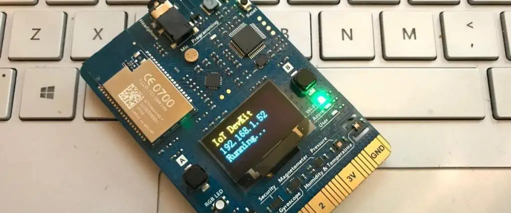
An IoT device features a sensor and then connected to the internet to transfer data from object to object or to people. This device is connected to the internet. Examples of IoT devices are computer devices, wireless sensors, software actuators, amongst others. These devices are usually attached to another device that functions through the internet and as such, it enables data transfer among people or objects without any human interference.

For instance, there are IoT systems in vehicles. These systems can detect traffic and then send messages of your delay to who you are planning to meet. A pacemaker is a good example of an IoT device. This device can interact with other machine to achieve convenience and more ease of life.

Iot devices are usually very small. They are portable digital machines that can be carried anywhere. In cases where personal computers arenโ€™t portable, IoT devices offer compactness and portability. Also, IoT devices help in gathering data and interpreting the collected data with machine learning AI.

Common examples of IoT devices are smart home devices such as smartwatches, Ring cameras, and smart home devices such as Google Nest. These devices are specially designed to function well in different applications. They help people to carry out their daily activities with ease. For instance, with the help of medical implants and devices, people can live active lives.

Furthermore, IoT devices prevent bottlenecks and possible problems in business operations. You can as well change the temperature of your home from anywhere you are. Isnโ€™t this amazing!

How Do IoT Devices Operate?

You canโ€™t fully comprehend how IoT devices work even if you have knowledge about the Internet of Things (IoT). IoT devices offer more than you think and as such, you need to have an understanding of how these devices work. IoT devices are like a mini-computer that transmits data to the cloud. After which, the information is processed by the cloud and a decision is made regarding the information.

For instance, the cloud software may adjust a sensor, display a notification, or send an alert. To have a better understanding of how IoT devices function, we need to take a look at the functioning of the IoT system. An integrated IoT system comprises four main components. These components are responsible for the performances of IoT devices based on their programming. They include sensors or devices, data processing, connectivity, and user interface.

Requirements of IoT Device Manufacturing

FULL PCB MANUFACTURING Quote

For IoT device manufacturing some requirements are needed.

Connectivity

It is possible to connect IoT devices to the internet via a wireless or wired connection. When manufacturing IoT devices, connectivity is a crucial requirement. This is because it enables IoT devices to interact with each other as well as the central server.

In IoT devices, there are different protocols and technologies that can allow internet connectivity. This includes cellular network, WiFi, and bluetooth. However, factors like power demands, data transfer needs, and the location of the device will determine the choice of technology. For instance, an intelligent irrigation system may integrate a cellular network for connecting to the internet. This is because this system might not be able to access a Wi-Fi network.

Sensors

When manufacturing IoT devices, sensors are always included. Sensors are needed for collection of data. IoT devices collect data from their environment through sensors. They can collect information such as sound, temperature, motion, and humidity. In IoT device manufacturing, sensors are connected or integrated via external means. This could be a smart hub or a sensor module.

Intelligence

IoT devices are specially designed to process and analyze the data they gathered. With this gathered data, they make decisions. These devices can carry out decision making via onboard software or by transmitting the information to a central server. In IoT device manufacturing, intelligence is an important requirement as it enables the analysis and processing of data collected and make decisions according to this data. An IoT device canโ€™t perform as expected if there is no intelligence. Therefore, intelligence is a crucial requirement during IoT device manufacturing.

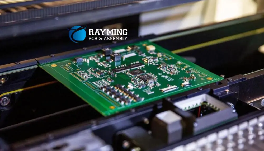
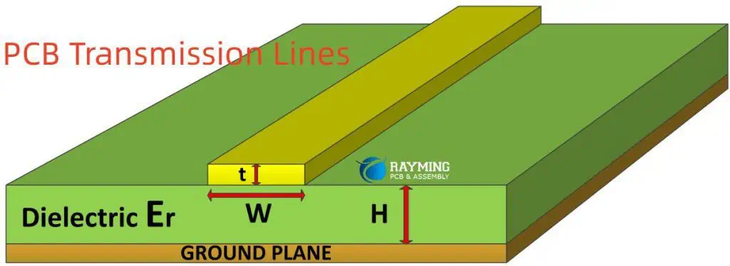
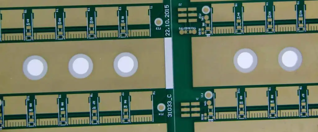
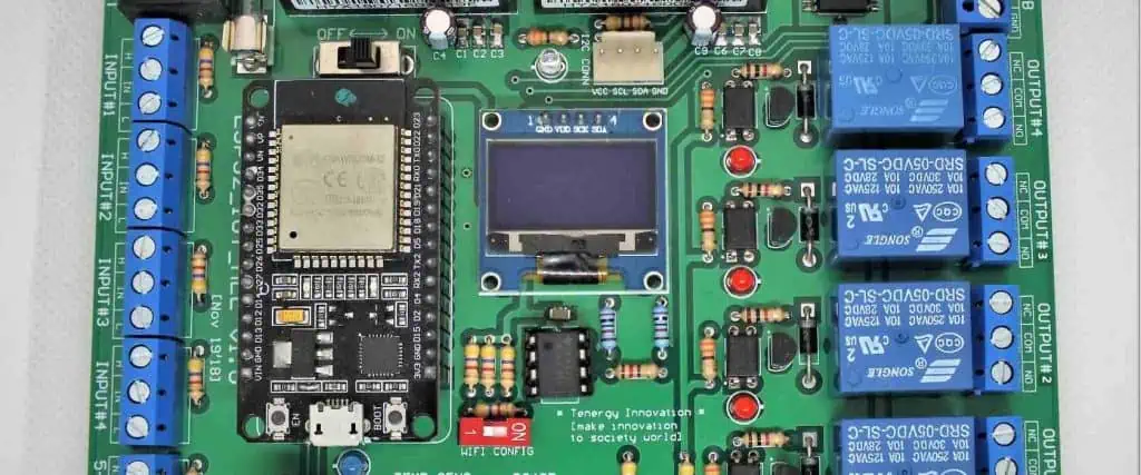
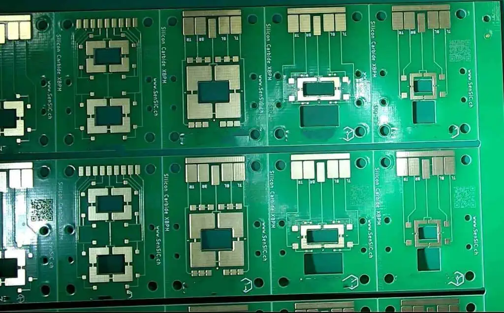
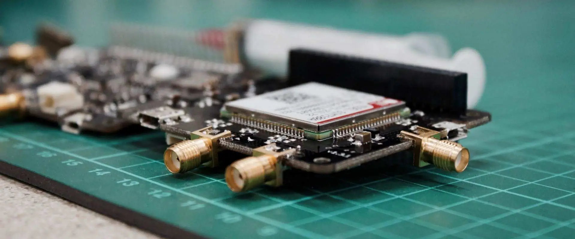
What is an IOT Device Control PCB?

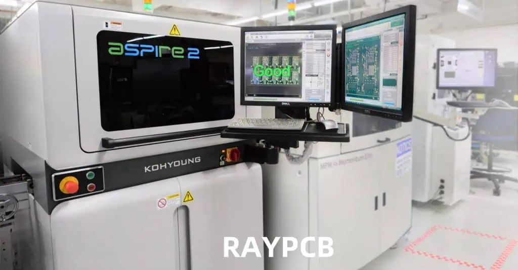
The printed circuit board is a crucial component of IoT devices. These boards serve as the foundational block for these devices. They connect all the components in the IoT device. Innovation and advancement in technology has made it very easy to design various boards with different sizes. Also, it has made it possible to design circuit boards with least complexity and better efficiency.

Circuit boards are an ideal choice for IoT devices. IoT device control PCB manufacturing requires careful attention and high level of precision. Proper IoT PCB design is a necessary measure to adopt in companies that manufacture smart electronics.

Board dimensions are one of the most crucial requirements for IoT devices. Also, physical limitations like size and flexibility should be considered during IoT PCB design. High optimization is required for battery design associated with energy consumption.

A communication network is always needed to connect IoT products. It is important for you to earn as well as maintain consumer trust as there is an increasing dependence on IoT devices. Therefore, during IoT device control PCB manufacturing, comprehensive simulation is paramount.

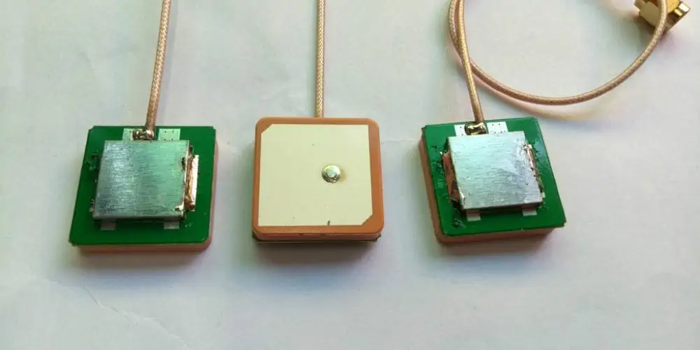
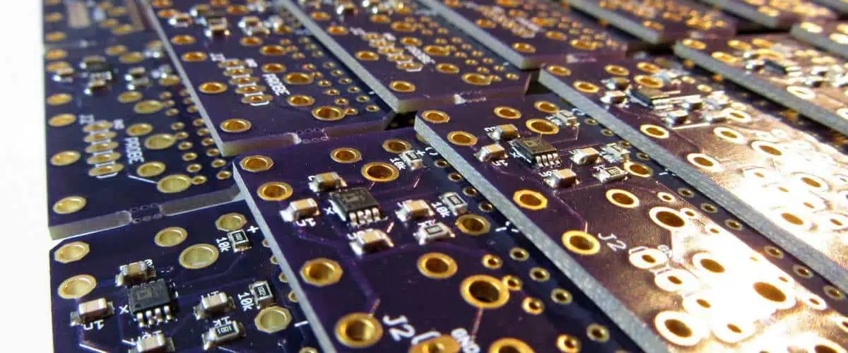
When designing new hardware products, it is advisable to put much attention on small size PCB design. A smaller PCB is needed for the manufacturing of a smaller hardware product. Small size PCB is necessary for hardware products such as wearables and other IoT related products. In such applications, it is highly recommended to go for high density interconnect (HDI) boards and flexible boards.

Some small boards are very complex to design. However, small boards with high performance are needed by various smart electronic devices. These boards donโ€™t encounter any difficult in supplying a good amount of electricity. Also, they operate wirelessly. Therefore, such boards require sophisticated PCB design techniques.

Importance of IoT Device Control

IoT device control offers the ability to access, detect, and manage the performance of deployed IoT devices. Some key factors explain the reasons for IoT device control. For instance, the size of network is a good factor. It looks at how accessible your devices are and their widespread geographically. Irrespective of the location or number, it is important to evaluate these devices and upgrade their capabilities. Also, you can use security patches to check if they are up-to-date and in compliance.

Use cases of IoT device control

IoT device control has found their use in several applications. Their use cases have been outlined below. You need IoT device control:

  • When there are many devices and you need to access them from a central location or a remote area for insights or firmware update about the functioning of the devices.
  • Devices are deployed in dangerous or inaccessible locations. For instance, some IoT devices are installed in wells, trains. Bridges and dams, manufacturing facilities, city intersections, and more.
  • When you need to stay alert to some particular conditions like an attempted security breach or a need to replace a battery.
  • There is a need for optimum utilization of your human resources.
  • Devices are installed in applications that are mission critical. In such cases, any failure or downtime can result in loss of revenue.

Conclusion

IoT devices are hardware devices specially manufactured to gather and transmit data through the internet. There are a wide array of IoT devices with distinct functions. However, these devices share some similarities in the way they operate. IoT device manufacturing has contributed to the development and growth of various industries. Even in human lives, there has been a positive impact.

There are a wide range of IoT device manufacturing companies. Examples include Google, Amazon, and Footbot. These companies manufacture a wide range of IoT devices. For instance, the Google home voice controller offers voice-enabled services such as volume control, lights, alarms, and more. Any questions? Please reach out

In House PCB Manufacturing vs. Contract Manufacturing

PCB prototype assembly suppliers

Different manufacturing companies always seek methods that can save costs, help to boost output, enhance quality, as well as modify their processes to be able to manufacture more sophisticated products. The production process of a company is a major cost factor whether it deals with the manufacturing of complex mechanical systems as well as distinctive electronics. In order to achieve all these objectives as well as manufacture new products, top companies are actively investigating and employing different techniques for innovative manufacturing.

Additive manufacturing is always unique among the possible methods necessary for raising productivity. This is because it can enable businesses to achieve the aforementioned objectives all at once. Additive manufacturing has grown into a competitive option to help boost productivity in different sectors.

Newer systems might be used for a full-scale internal PCB manufacturing of complex items. These include cutting-edge electrical components.

What Does In House PCB Manufacturing Entail?

You can say goodbye to cost-intensive tasks such as making payment for shipping fees, evaluation of the vendor profit margin, budgeting for any delays, prevention of possible hassles, overcoming the language hurdles, and others. These are great benefits. All the pitfalls related to the exportation of your designs would suddenly disappear. This leaves you with additional cash savings that you can divert to other important areas of your business.

The finest aspect of this advantage is that you may save more money the more you produce. Consider this while making a choice on the subject; you could quickly realize that your investment in 3D printing will pay off handsomely.

When developing and fabricating PCBs for one-of-a-kind electronic items, you want a flexible internal PCB manufacturing system that offers reliable lead times as well as pricing for complicated, low-volume products.

Advantages and Disadvantages of In-House Manufacturing

through-hole assembly process

The major advantage of in-house manufacturing is that there are almost no discrepancies in the design, manufacturing, as well as other phases of the entire process.

Pros

Faster turnaround times are considered to be among the most significant of all benefits of in house PCB manufacturing. With all outsourced prototypes you purchase, you’ll need to place these things on hold for about a week. This doesnโ€™t include expedited orders, which are usually expensive.

Reduction in time of about 80 to 90% of all prototypes manufactured using the in house 3D printer. This is due to the fact that each 3D PCB can only be assembled once every 24 hours.

Beyond the time savings, businesses which outsource their manufacturing operations are far less likely to take the plunge with each iteration. This is why design engineers canโ€™t work as rapidly as they might with in-house machinery that greatly reduces the pace of development. At this pace, engineers might make their choices very quickly and with higher agility.

Returning to the time savings, this ability to quickly develop and iterate designs makes it very simple to run via a variety of variation testing. Imagine the amount of variations you might go through in order to confirm, reaffirm, and confirm with that additional savings of, assume, six days.

Cons

While in-house manufacturing offers some benefits, it also comes with some drawbacks. Below are some of the things you need to think about.

As already said, the main disadvantage of PCB in-house manufacturing and electronics manufacturing involves the huge cost of setting up your fabrication unit, the testing equipment, CNC machines, etc.

It also required knowledge. Due to this, one might need to recruit professionals in relevant fields. Building different vendor networks for the procurement of components is important if you wish to receive the best components possible and in a timely manner given the enormous quantity of network, resources, and cash available. Also, you must possess a logistics unit and supply chain to achieve this.

This is a very important component for storing components, inspected goods, finished goods, and exported goods. You will need a sizable warehouse equipped with reliable pallet racking systems, material handling tools, as well as inventory management software.

You must adhere to specific industry norms and rules. Also, you may need to have some certificates because legal repercussions might happen whenever something is wrongly done. Overall, you must make some investments in technology, machinery, and other things.

What Does PCB Contract Manufacturing Entail?

Printed circuit boards are designed, manufactured, and assembled through the utilization of different standardized and very accurate manufacturing techniques.

When manufacturing and mass producing electronic items, it is important to have consistency of performance as well as compliance with the standard manufacturing techniques. Without very advanced machinery and highly qualified workers, PCB Contract Manufacturing implements some quality and performance which isnโ€™t otherwise attainable.

Another problem handled by PCB Contract Manufacturers is the strict requirement for component homogeneity in addition to the appropriate positioning of components, including LEDs in the lighting devices.

What are the Advantages of Contract Manufacturing?

FULL PCB MANUFACTURING Quote

Aside from cost, contract manufacturing comes with some advantages. The only thing left to achieve involves finding as well as choosing a skilled and reputable provider for your PCB contract manufacturing after completing the eventual design of the product. This addresses half of the issues using in-house manufacturing. Below are a few advantages.

The contract manufacturer is well equipped with the necessary human resources, infrastructure, as well as service structure. These include a fabrication unit, an assembling unit, a warehouse, a supply chain, and more. They will need precise, in-depth designs to help create and put your product together. They handle the selection of the parts, materials, the actual production design, the inspection, and the complete process.

In this instance, you may request a prototype, have a design reviewed many times, request adjustments if necessary, and more. Since the majority of contract manufacturers employ knowledgeable and experienced designers and engineers on staff, they help you at every level.

The PCB contract manufacturer would have developed a wide network of vendors because there are several possibilities for buying the parts and supplies needed to make the circuit board. A CM will locate the best solutions from producers, distributors, as well as brokers in its supply chain using a variety of software programs to get the part component and update information.

According to this payment arrangement, you do not need to pay everything at once but rather in installments. You gain from a great deal of flexibility, the customization choices, a shortened time to the market, as well as several other advantages.

You have more time to devote to researching and learning about your area of expertise, documentation, related research, etc.

In House PCB Manufacturing Vs. Contract Manufacturing

In what ways does “In house PCB manufacturing” differ from “Contract manufacturing”?  The choice of whether or not to work with contract PCB manufacturers might be significantly influenced by the distinction between the two. Let’s look at how these elements compare to one another before discussing what they are.

In-house PCB manufacture might be a great choice for your manufacturing requirements. This depends on some important aspects.

Flexibility

Flexibility is the initial requirement. A design might alter or improve at any point, and it’s extremely possible that this may happen while a project is in the stage of manufacturing.

It is easier for users to update files and quickly execute the modification of the design during in-house manufacturing. Generally, working with contract manufacturers might make the entire procedure difficult. However, for in-house manufacturing, RayMing PCB can work with identical flexibility as indicated before.

If thereโ€™s a need for design modification, RayMing PCB is fully equipped with the necessary processes to carry out the change as efficiently as possible coupled with reducing any probable losses. Customers can email us their new files, and the manufacturing will be updated immediately.

Quality Improvement

Quality improvement is another important factor. It is easier to manage your product’s quality when it is manufactured in-house. Employing contract manufacturers often comes with higher risk because they can have other projects at hand in addition to yours. It makes sense that orders for bigger quantities would be prioritized above orders with fewer quantities. No matter how many orders there are, they are all handled using identical quality control techniques.

Control over manufacturing

Control over manufacturing is another significant component. When producing in-house, it might be desirable to take responsibility for spikes in production and apply techniques to control them via resource planning. Moreover, there may be instances when there isn’t enough labor or equipment available to fulfill the supply and demand when depending on the in-house productions. In these circumstances, outsourcing can be the sole feasible solution for meeting deadlines.

RayMing PCB’s great resource planning enables us to take production surges into account and make sure that they can always fulfill the demand of clients. They always consider the requirements that may affect the lead time starting with the quote. They will let you know about them in advance even before you place your order.

For your demands, RayMing employs cutting-edge equipment. For more information regarding the capabilities of printed circuit boards, visit our website. In order to guarantee that the created designs are secure and donโ€™t face any danger of losing their intellectual property, RayMing is also delighted to sign a confidentiality agreement with their customers.

Saves you money and time

Lastly, in-house manufacturing often saves you money and time from the logistical perspective. Transporting goods that are necessary for the industry will no longer be necessary, especially across the international borders. Such transportation expenses might be occasionally equal to the cost of the initial creation of the goods.

RayMing PCB & Assembly reduces these expenses by providing all your supplies for you through our company’s full-turnkey services, serving as a single source for your project requirements. Allowing us to handle every aspect of your projects from beginning to end comes at no extra expense. If necessary, we may additionally accept the hassle-free consigned components to us and will constantly work alongside your company in this respect to lower your total expenses.

Why Choose Contract PCB Manufacturers?

pcb-assembly-san-jose

Using the contract manufacturers for your PCB assembly projects has several benefits. Here are a handful of the more significant ones. In light of that, let’s examine them.

Speed of Production

Excellent product quality, as well as a short lead time makes up two essential requirements for creating a successful PCB assembly. Experienced, reputable, as well as competent contract PCB manufacturing businesses offers both a decreased lead time and excellent quality. This is possible thanks to the development of facilities and technologies. These circuit boards undergo testing to prevent additional problems and malfunctions.

Minimal design period

For many makers of electrical components, the time required for developing circuit boards may be a major challenge. This is due to the fact that depending on their complexity, the circuit board assembly as well as the manufacturing process takes time, depending on the components used, layers, complexity, and other factors.

Nevertheless, the contract manufacturer would get through these problems as well as certain other design obstacles since they possess the necessary training and experience.

Circuit board manufacturing one-stop shop

One major advantage of using a contract PCB maker is this. From conception through installation and even beyond, highly skilled businesses will provide full solutions for your printed circuit board requirements. As a result, you won’t have to work with different businesses to assemble the different components. From the designing of your circuit boards to the overseeing of the entire production process, they take full control. Additionally, they ensure logistics of the supply chain, which is a significant problem for many manufacturers of electrical components globally.

Conclusion

Although in-house manufacturing may offer much freedom, please take note that, given the appropriate alliance, the contract manufacturer might actually offer greater flexibility. This is because the contract manufacturer already possesses the specialized tools and resources required to adapt production for marketing variations. The production process of a company is a major cost factor whether it deals with the manufacturing of complex mechanical systems as well as distinctive electr

What is a Chip Antenna and How Does it Work?

rf antenna chip

The behavior of the chip antenna is very unpredictable since an antenna can function when used as a facility for testing and when it is finally integrated into the device. However, we cannot say this about antennas.

What Does a Chip Antenna Mean?

The chip antenna is a unique antenna, well-known for a compact footprint. In order to emit high frequency electromagnetic waves, they are frequently incorporated in circuit boards. They are ideal for tiny devices such as mobile phones and WiFi routers due to their constrained range.

The main distinction between the ordinary antenna and chip antenna is its tiny size, although both can transmit and receive electromagnetic waves. Taking their quality into consideration, they are not expensive. Whenever the larger-sized antennas are not feasible, the antenna on chip is the best option.

Making use of fractal geometry is a reliable way of designing an antenna to be added to the printed circuit board. This fractal geometry can be described as a complicated pattern created by repeating a basic form that lengthens the material’s perimeter or optimizes the length of that material emitting electromagnetic radiation.

These antennas should match the wavelength of the signal; also, the fractal pattern must be preserved in at least two distinct ratios. These antennas, which can be tailored to fit different footprints, can also be seen in mobile gadgets. Generally, fractal antennas have remarkable bandwidth and gain. The designs for fractal antennas don’t require any additional parts to function. This ensures its flexibility further.

The Design of Chip Antenna

Chip antennas provide small and portable solutions for wireless products. They simply require a little room and some ground clearance. Users receive performance which is marginally inferior to those of larger antennas including PIFA, patches, as well as dipoles in exchange. However, there are some limitations that you need to take note of.

Watch out for the ground planes

Actually, a chip makes up just half of an antenna design. The PCB’s ground plane constitutes its other half. Similar to the monopole, the form as well as size of ground planes have a direct impact on the pattern of radiation as well as tuning of the antenna on chip.

The majority of datasheets will list the antenna’s maximum gain, return loss, bandwidth, radiation pattern, as well as other characteristics. They would also comprise a drawing. Have you noticed the PCB’s dimensions? Measurements taken from this specific ground plane served as the basis for all reported performance numbers. It’s quite possible that the chip antenna that you incorporate into your device will fit onto a PCB with a different dimension. Hence, the performance will be different from what is shown in the datasheet. Also, since the performance evaluations were conducted outside, the antenna will probably be contained within a product.

Layout for the Chip Antenna

Note that you can only place metal near the chip antenna on specific sides. You should position the chip in one corner only with the ground on both sides. It is wrong to position the chip through the three sides, which now becomes perpendicular to the earth.

As previously mentioned, the antenna would be impacted directly. Performance declines when the ground becomes closer than usual. Performance also changes when the ground gets farther away than normal.

Differences between the Printed Antennas and the Chip Antennas

What does printed antenna mean and how does it work

Your PCB is useful for printed antennas, commonly referred to as microstrip antenna. They are also composed of a unique geometric design located on the top region of the copper plane with precise lengths and widths to fit the impedance and frequency of the emitting circuit. Many patterns, such the inverted F, circular, straight trace, and others, are relevant in this case.

The printed antenna could be thought of as a simplified, scaled-down variation of the conventional wire antenna. With respect to the dimensions of the microstrip traces and copper planes, this can hold different frequencies and impedances.

Understanding the chip antenna

Chip antennas are constructed as dielectric-filled ceramic cavities between conducting surfaces known as the dielectric resonator antenna (similar to the way ceramic capacitors are built). It produces the stationary wave and is referred to as the cavity resonator. Similar to PCB antennas, this same impedance and frequency also depend on the shape of the conducting surfaces, but because the materials have a high permittivity, the antenna’s size for same wavelengths could be reduced significantly.

Asides how both antennas were built, how do they differ?

During the development of both antennas, there were some factors to consider. The most obvious of all these factors is the size. It is important to take note that relative to making use of the chip antennas as a tiny component, designing with the use of printed antennas needs a larger space for the traces and copper planes.

Another important factor is the climate and temperature. The electromagnetic interference of close circuits will most likely affect the printed antennas. Also, the antenna region must stay free from all conductive components and traces across all levels since the metallic objects close to the antenna’s irradiation area, including all other copper layers on the Circuit board, might limit the performance.

While 50% of the performance and effectiveness of the chip antenna depends on the execution of an efficient ground plane, the chip antennas are less susceptible to this problem but tend to become more delicate towards the noise that originates from the ground planes.

What is the Performance of the Chip Antenna?

FULL PCB MANUFACTURING Quote

The effectiveness of the chip antenna would be changed significantly by the following factors. Letโ€™s quickly consider each of them.

Layout

The effectiveness of the antenna on chip is significantly influenced by how the components are spaced and positioned on the printed circuit board. Chip antennas should have ground planes that have the right size and are well located in order to create a full resonant circuit.

A dipole would be created by ground planes with a length of 3 to 4 cm, as well as a breadth of 1 to 2 cm. However, if this plane is larger, it would act or function as a monopole antenna. This PCB can function as a ground plane. However, the antenna itself has to be mounted and placed on the edge of the printed circuit board. This is located on the top section, which is isolated from the remaining parts of the board and free from metal objects that could affect or interfere with its radiation.

Moreover, both the microstrip line and ground plane has to be proportionate. The feedline must be as short as possible in addition to being perpendicular to the microstrip line. This is to avoid becoming a parasitic component of the resonance system. The vias, which are carefully positioned through the holes in the board, helps in reducing the electric field created at the edges of the printed circuit board.

Panel chip antenna selection

Because of their widespread use in many portable devices, chip antennas were built within rubberized or polymer enclosures. This helps in shielding the circuit board from some damaging elements such as stress, vibration, dust, moisture, or chemicals.

Casings and metal parts should be kept to a minimum. In addition, the radiation pattern of the chip might be affected by these enclosures and casings. This is why they have to be examined properly and carefully.

What are the Benefits and Drawbacks of the Ceramic Chip Antenna?

The use of ceramic antenna comes with different advantages. For instance, it reduces the need for modeling software and takes away the expensive fabrication of fresh prototypes. This is because the antenna lacks physical qualities and needs network tweaking. Generally, this is economical because you won’t be wasting components as a result of continuous prototype manufacturing.

Other benefits of the ceramic antennas include:

  • It has different setups
  • Reduced size
  • It is less susceptible to noise from components and the environment
  • Ceramic antennas accommodates modifications to the design guidelines of the PCB design guidelines
  • It is less simulation-intensive.
  • It is very easy to replace

However, ceramic chip antennas have some negative side-effects. These include:

  • Higher initial costs such as the purchase price of the ceramic chip antenna as well as the need for its auxiliary components. The cost per unit ranges from around $0.10 to $1.60 on average. However keep in mind that this is an average price, not its maximum price.
  • This PCB trace antennas performs better compared to the ceramic chip antennas.

Overall, because a ceramic chip antenna is introduced to a circuit board after the phase of the design has been completed, it offers more tuning flexibility. As they use the surface mount arrangement, they also allow quick hardware upgrades.

The ceramic chip antennas allow you greater room as well as openness in the design. This enables the usage of further components for every stack. Also, this enables the utilization of smaller printed circuit boards as well as the addition of more components. This results in a better overall cost-effective design. Moreover, you will definitely see a huge rise in savings if you have a multilayer design.

What Does Antenna Matching Mean?

5G Microstrip Antenna

Antenna matching can be described as the process involved in modifying the design so as to ensure the other radio frequency circuits on the PCB and the antenna’s (module or chip) impedance are properly matched. To construct an effective and productive antenna, this impedance should be around 50 ohms. This is because interference from nearby components on the PCB or the housing can alter the frequency of an antenna.

One reliable method of achieving this is to include the impedance matching circuits in the design. Antenova advises using the pi (TT) matching circuits so as to allow the tuning as well as optimization of the antenna. For the single band antennas, pi matching circuits may include three components (capacitors and inductors), or even more for the multi-band antenna. Also, this serves as a helpful approach to adjust an antenna’s performance within a design, especially in practical situations when the antenna must work in less ideal locations, including while being held in the hand and worn on a person’s body.

Furthermore, the co-planar grounded wave guide advised whenever the embedded antenna is placed on a PCB. This eliminates the need for vias, which is preferable because they contribute loss to a transmission line as well as inductance into these matching components. This leads to erroneous tuning values.

Market Trends for Chip Antennas

Chip antennas are small antennas that transform radio waves into electrical signals and vice versa. The proliferation of the chip antennas in the IoT devices, a rise in the demand for the smart antennas, the prevalence of internet, the rise in Smartphone usage, and improvements in the 5G technologies were the main factors propelling the market’s expansion.

However, the lack of a consistent frequency spectrum for different wireless applications could impede market expansion. On the other hand, over the projected time, the development of the 5G technology will present an enormous chance for expansion for chip antenna markets. On the grounds of end user, type, application, and region, this chip antenna market can be broadly categorized.

The dielectric chip antennas and LTCC chip segments of the market are separated by type. Bluetooth chip antenna, multi band/dual band, GPS/GNSS (gps ceramic antenna), WLAN/Wi-Fi, nfc chip antenna and other applications make up this application segment. This market is examined by the end user and also broken down into segments like healthcare, consumer electronics, automotive, and telecommunication.

Conclusion

We hope we have been able to explain what chip antennas are. Antennas, which form the major components of the RF devices, have a huge impact on the way they work. The main criteria for current RF applications are high performance, reduced size, as well as reduced cost.  There are many advantages to using the Ceramic Chip antenna. The most important of all is that it does away with the need for pricey simulation and prototype production softwares.

Reasons Why PCB Transmission Lines are Important

pcb transmission line

Whenever you consider transmission lines, the first thing you will think of is cables. Although this isnโ€™t our focus in this article, the PCB transmission lines act in a similar way. While the regular cables will help transfer electricity between two points, the PCB variants help in transmitting signals from and to the transmitter and receiver.

However if you are not familiar with the way it works, the integration of transmission lines into the PCB layout could be a challenging process. However, we will be providing you with all the important information before you make attempts to add then into your high-speed designs. We will be discussing the types of PCB transmission lines, their significance, and more.

What Do PCB Transmission Lines Mean?

The PCB transmission line is made up of linkages useful for transmitting and receiving signals from the board.

Also, they are made of two conductors, signal trace, as well as a return path. Dielectric material, such as PP, Coverlay, and fiberglass, make up this thickness that separates these conductors.

Furthermore, PCB transmission lines carry all the I/O signals. Signals are transferred from one location to another using a reference plane and signal trace within the single ended input/output connections. However differential I/O combines two traces using the reference plane to create the transmission lines.

Which are transmission lines and which ones are not?

Transmission lines wonโ€™t be necessary if the frequency of a signal on the electrical wires remains low enough to denote that the wireโ€™s voltage at any specific time is constant over the whole length of the wire.

However, transmission lines should be used in this situation instead of just the usual connection when the traveling signal’s frequency is very high and you have a very long PCB trace length.

Whenever the interconnect is no less than 25 percent of the length of the signal’s wavelength passing through, you can refer to it as a transmission line.

Impedance-Controlled Transmission line

PCB Transmission Lines

A transmission line‘s alternating current features a frequency high enough to exhibit characteristics of wave propagation. The main factor affecting how electrical signals travel down transmission lines is their impedance, which exists along their entire length assuming the line maintains a constant shape.

This line is referred to as controlled impedance lines. Distortions and signal reflections occur due to non-uniform impedance. To forecast the signal’s behavior at high frequencies, the transmission lines must have a regulated impedance.

To prevent any crosstalk, signal reflections, electromagnetic noise, and other problems which may affect the signalโ€™s quality negatively and lead to mistakes, it is very important to consider the impacts of the transmission line.

While it isnโ€™t necessary for the signals to feature a reference plane, it is required for the actual implementation of the differential traces on the printed circuit boards. Transmission lines having regulated and controlled impedance are essential for maintaining great signal integrity within a printed circuit board system. The reference planes, the signal traces, as well as the shape of these traces all affects the impedance.

The presence and lack of glass within a specific lamination weave may lead to impedance variation. However this hardly causes problems outside the high-speed connections.

What Kinds of Transmission Lines Are There?

Microstrips and striplines are the two main signal transmission lines that you can find on printed circuit boards. On the topmost layer of the board, these microstrip transmission lines are made up of a single uniform trace. Also, the trace usually runs parallel to the PCBโ€™s ground plane.

What else? The traveling signal has a return route, which is provided by the ground plane. To prevent any contact between the ground and trace plane, a specific height of dielectric material would be helpful.

Contrary to this, stripline PCB transmission lines feature a single uniform trace within the inner layer of the circuit board. Additionally, parallel dielectric layers and conducting planes give a transmitted signal two return pathway. This separates the trace on either side.

Asides from the usual types, you can make use of a third category on your printed circuit board. However it’s quite uncommon. This return path and the signals trace are located on the layer of the board.

However, the signal trace, stays at the centre, with two neighboring ground planes also surrounding this trace. Additionally, the structure of the transmission line is where you may discover the dielectric substance. Coplanar structures are also an option for striplines and microstrips.

Microstrip

It consists of one uniform trace (which is designed for the signal). Also, it is parallel to the conducting ground planes on the top layer of the PCB and serves as the signal’s return path. A particular height of the PCB dielectric separates the trace from the ground planes.

Stripline

On the innermost layer of the PCB, there is a consistent trace known as a stripline that carries the signal. The parallel circuit board dielectric layer and the conducting plane are used to divide the trace on each of the sides. As a result, the two reference planes are its two return routes or paths.

Coplanar

In the coplanar waveguide setup, this conductor for the return path is on a similar layer within the printed circuit board as a signal trace. The three flat surfaces are referred to as “coplanar” because they are all on a single plane, with a signal trace in the center and the two adjacent exterior ground planes surrounding it. Underneath is where the printed circuit board dielectric is situated. Coplanar structures are possible for both striplines and microstrips.

Considerations for Transmission Line Design

FULL PCB MANUFACTURING Quote

There are a few aspects that must be taken into account when joining traces on the printed circuit board design. Below are some pointers to assist you with this.

The transmission lines comprise groups of at least two ports that serve as the receiving and generating ends of power. This is why, the majority of transmission lines are required to have conductors. Three conductors are required if your lines are three-phase. Coaxial cables or common PCB traces can also be used as lines for transmission.

When the circuit size is tiny and the wavelength is short, transmission lines operate differently. Additionally, the loop inductance all through the length of the conductor and the capacitance in-between both conductors will also affect how they function.

Although you could believe that transmission cables pass signals across various locations, there are other factors to take into account. Although that is the primary purpose, we advise carefully planning the design of the transmission line. Otherwise, the functionality of the PCB will be hampered by flaws in your transmission line and trace designs.

Importance of Transmission Lines in PCB

The transmission line in PCB plays an important role in reducing serial link loss and other associated expenses. This holds true for all high-frequency circuits since they are more likely to experience dielectric losses and signal interruptions. Therefore, during the process of design, it is essential to thoroughly consider and finalize the modeling and format of the transmission line modeling.

Thankfully, with great improvements in fabrication technology, modeling of integrated circuits, as well as higher operating frequencies, digital circuit designs may now be used for microwave and radio frequency connections. To properly connect the traces on the circuit boards, it is crucial to take into account some factors relating to the transmission line. Here are some guidelines that can be useful in this situation:

The transmission line effects in PCB is made up of a network of at least two ports which features both the power production end as well as the receiving end. Three conductors must be used for three-phase lines. Transmission lines might be made of regular PCB traces or coaxial cables. Because high-quality conductor materials or a sizable surface area within these conductors lower the resistance, the resistance needed within a PCB and the application must be taken into account. This is why there is an inverse relationship between these two variables and resistance. This holds true for lengthy circuit routes and broad wavelengths.

Fortunately, better solutions are becoming accessible as transmission lines are taken into account for uses other than resistive as well as low frequency ones.

Short wavelengths as well as small circuit sizes cause the transmission line to behave very differently. The transmission line’s loop inductance throughout its length and the capacitance between both conductors at a specific length both play a role.

Conclusion

Hope you understand what pcb transmission lines are. Impedance is a very important aspect you must consider during the construction of a PCB transmission line. Otherwise, if this impedance fails to match the length of the line, signal reflections would stop the entire process. Therefore, it is advisable that you estimate the PCB designโ€™s physical properties to manage the impedance of the trace lines. This then enables the system to keep a constant value.

Do you have any further inquiries on this article? Please reach out to us immediately; we’ll be pleased to assist you the best way we can.

The Beginners Guide to Gerber File Extensions

gerber viewer

The utilization of Gerber files forms a significant section of the circuit board creation, as well as diagnostics. In this article, you will learn much regarding the Gerber file extensions. These include the software required as well as those extensions that you will need to recognize. Before we go into details regarding Gerber file extensions, we will first consider what Gerber files are.

What is a Gerber File?

The Gerber file can be described as a unique 2D diagram that represents every layer of the printed circuit board whereby different shapes and lines represent vias, tracks, and pads. Explaining further, we mean that this is a way of mechanically instructing the printing machine to help in crafting the PCB board of your choice, with respect to the information given.

This unique method for manufacturing the PCB boards can be described as the most acceptable option amongst the manufacturers and designers because it is very specific and hardly experiences errors. Furthermore, all the information regarding the circuit board like track width and length, copper amount, as well as hole spacing, will be stored inside the Gerber File. Also, this style of data collection is very important to the PCB construction in order to help it achieve its purpose. The fileโ€™s final version seems to be a digital circuit board having all components attached to it.

What Do PCB Gerber File Extensions Mean?

RS274X Gerber File
RS274X Gerber File

Manufacturers work with a PCB design software for creating Gerber files used in upcoming electronics. Moreover, this process has to do with the CAD tool you are making use of. Nevertheless, the machines usually fashion the Gerber files, with respect to the Gerber format (RS-274X) that superseded ineffective and ancient forms such as the Gerber standard (RS-274-D).

Also, you can note that the Gerber data doesnโ€™t need any identifying name like text files; moreover, it is usually associated with some extensions like .gbr or .gb that are also viewed as the standard PCB Gerber file extensions.

Asides from this Gerber file extensions list, there are other types of Gerber files used. This depends on the PCB design software of the manufacturer.

The Standard Gerber (RS-274-D)

This can be described as the oldest representation of gerber files. The RS-274-D was known to support basic capabilities for plotting such as drawing trucks. This didnโ€™t define margins and coordinates of drawing distinctly.

Soon, this standard gerber suddenly became unpopular, which eventually led to its revoke by developers back in 2014.

Extended Gerber (X-Gerberโ€™s RS-274)

UCAMCO introduced this Gerber in 1988. It is useful for ASCII commands that are human readable, which are combined to create 2D vector graphics. Also, X-gerber integrates the utilization of metadata for defining graphics. It associates with the .gbx and .gbr gerber file extensions.

Gerber X2

The Gerber X2 is the most recent Gerber file format. It features different improvements for the earlier file formats. Gerber X2 supports all additional vendor extensions such as โ€œ.botโ€ and โ€œ.topโ€. Also, this file format works with majority of todayโ€™s CAM software programs or applications.

How to Open a Gerber File

Below is a guide for opening a gerber file. Before you begin, thereโ€™s a need to identify the type of file. These gerber files are usually saved in ZIP or RAR format, which corresponds to the specific layer of the PCB layout. Each one comes with its own gerber file extension.

Before opening a gerber file, click on File and then open it from your menu bar. When it comes to viewing the gerber files, make use of the program called Gerber Viewer. There are viewers that require installation, some others can easily be checked or accessed online.

Whatever the case is, you have to choose a viewer which supports contemporary file formats. In addition, you must choose one, which allows the taking of precise measurements, and zooming in. This assists you in testing of the circuits as well as adjusting the board.

More Information

Also, you may have to download a unique online gerber viewer. This aids in simplifying the entire process. In addition, the most important aspect when opening the gerber file involves making sure that it works with your choice of software.

In order to ensure compatibility, thereโ€™s a need to name the file making use of a similar convention with the program. You can either regenerate or delete them when theyโ€™re incompatible. Also, to be able to locate the best possible viewer, choose or click on File, then click Open Layer(s). Here you will find numerous programs that will open as well as edit the Gerber file, some of which are free, while others are paid for.

You may make use of ViewMate and other comparable free programs. These are user-friendly applications and they also provide advanced features. Also, you will be able to view all the layers, go ahead to modify every layerโ€™s visibility, as well as measure the distance found between the components.

In addition, these programs donโ€™t allow users to save the drawings. However, they play an important role in verifying your designsโ€™ accuracy. These applications will also be useful and important for quoting.

Different CAD Softwares Used for the Gerber Files

FULL PCB MANUFACTURING Quote

Computer-Aided Design or CAD involves the designing, developing and drawing of the PCB using computer software. The programs used are called CAD Software.

There are different circuit design softwares that work to meet the requirement of the diversified layout that the manufacturers have requested for. These include the online free circuit board design software, industrial PCB softwares, as well as the free printed circuit board design software.

In this section, we will be considering some reliable CAD as well as Gerber Viewer softwares which are commonly utilized in circuit board manufacturing.

Altium

Altium features the Protel form of Gerber file extension and is known as the most comprehensive and modern CAD software globally. It was specifically designed for manufacturing PCB board and has maintained the best option among the engineers and designers all over the world.

In addition, Altium didnโ€™t just attain huge success overnight, as this current version has been able to evolve through many decades of development and innovation. Currently, Altium gerber file extensions are now at a stage whereby it has the ability of creating a unique and unified environment, which features the required tools for meeting the requirements of the design.

KiCad

This can be described as an opensource software and gbr file reader. Also, this software acts in line with the copyright agreement of the GNU. Just like the other CAD softwares. KiCad offers designers and manufacturers with a user interface that is graphical that aids in board construction.

In addition, you donโ€™t need to utilize any specialized devices when working with the KiCad software. Just the keyboard and mouse are okay. Furthermore, it works on two main operating systems, which are Linux and Windows.

As you run the software, designers would see that KiCad offers some support for schematic diagrams, PCB layouts, stable model view in 3D, viewing of the Gerber file, and lots more. Also, this application includes 3D libraries, symbols, and packages, which comes as bonus for users to download.

Eagle

Eagle features reliable functions as well as a user-friendly interface that aids in the construction of your circuitโ€™s schematic diagram. In contrast to the other products, Eagle gerber file extensions requests that users pay a fee, which is financially acceptable, before making use of its features. The truth is that the price charged is worth it because it comes with great features such as online positive and negative annotation function, batch command script files, copper cladding, and interactive follower.

Also, it is very important to note that EAGLE offers support for many platforms, which includes Mac, Windows, and Linux. Also, it comes with usable scripts, a very rich library, as well as CAM tools. All these are great options for the designers of PCB boards that have the ability of working with EAGLE gerber file extensions.

OrCAD

This program has been available since late 1980s. In fact it is almost the same age as Altium. This application is well-known among different manufacturers as a result of their simple operation, simulationโ€™s important function, and a friendly interface for the users.

Immediately the schematic diagram has been imputed, the information system of the component is included, which plays an important role in authenticating, creating, and tracking of all the PCB boardโ€™s elements.

Also, all these features combine together, making it a great and reliable option for all dedicated manufacturers. Though OrCAD isnโ€™t regarded as the most effective CAD software in the market, it comes with a great management function as well as an environment that is well-integrated.

PADS

This software is widely regarded as the boss of CAD due to the fact that it is comprehensive and user-friendly. In addition, the quality of the design is better and impressive compared to other applications such as Allegro.

Furthermore, PADS is regarded as a good choice in the marketplace, and is usually utilized by small companies. This is because it is comprehensive, affordable, and user-friendly. This software also covers different functions such as assembly files, schematic diagrams, output of the bill of material, and more.

How to Convert Gerber Files to PCB Files

Figure 6 Gerber files enable and disable and extensions

 In order to convert your Gerber files into PCB, go to the Manu (Export Format) and then choose that Gerber file. Next, deactivate your โ€œSkip Options Dialog.โ€ Then, choose your PCB file and click โ€œNext.โ€

Once you are done choosing your PCB file, your Gerber file would appear in that folder containing the PCB file. Once you are done converting it, this PCB file would be available for editing. Most electronic designer export their designs to take the form of gerber files before sending them to the facility used for PCB fabrication.

These files make up the universal language for PCB design. Also, the equipment for PCB printing wonโ€™t understand the design in their absence. If you want to create PCBs, thereโ€™s a need to understand how you can generate the Gerber files. Take note that ASCII is its file format. This means that you can edit it using text editors.

From your file menu choose โ€œGerber Export.โ€ You will see all the PCB layers displayed in your PCB export tab. Also included are silkscreen, mechanical, drill template, as well as electrical template layers.

Then, select โ€œCreate Artworkโ€ for generating a printed circuit board document that contains all layers. Also, you would need to type in the PCB documentโ€™s parameters. There are many online programs, which allow users to edit their gerber files.

Choose one that offers support for different output and input file types. Also, the software permits necessary modifications into the design as well as save it in whatever format that pleases you. Furthermore, many programs offer support for different file formats. This allows users to make use pf the Gerber Converter in creating the printed circuit board, which best suits the design.

Important Features You Should Look Into For the Gerber File Viewers

In order to select a reliable gerber file viewer, there may be a need to look into the following features.

Have wider printer compatibility

The viewer for the gerber file has to be compatible with different printers. Asides from this, it must have room for different printing alternatives for different printers.

Supports precision during viewing

Great gerber viewers must add features related to precision and zooming measurements ensuring that you check through the circuits as well as rectify all errors easily.

Support Modern File Types

A reliable gerber file must have the ability of supporting well known modern files such as Excellon and HPGL/HPGL-2 among others.

Conclusion

To conclude, the Gerber file can be described as animated diagrams that represent every facet of the circuit board where different shapes and lines represent vias, tracks, and pads. In addition, the Gerber file extension comes in different forms; however, the .gbr format is regarded as the standard.

Also, creating your Gerber file will need CAD software which also functions as the gbr file reader. Every application features unique benefits. However, we hope that our article was able to clarify what Gerber file extensions are.

What is EMS PCBA?

EMS Electronics Manufacturing Companies

EMS PCBA, which is also described as the EMS PCB assembly, comes with many applications and advantages within different technology fields. This EMS denotes electronic manufacturing solutions or services, while PCBA denotes the assembly of printed circuit boards. Careful planning as well as being attentive to detail is very necessary in placing and spacing of the components, sizes of the hole and location, spacing of the component lead, components selection, as well as other considerations regarding the layout of the printed circuit board.

The EMS PCBA process deals with manufacturing many complex components and might be composed of different services like component procurement, engineering design, fabricating and assembling the PCB, functional testing, and box builds.

When handling product builds, the appropriate EMS PCBA execution reduces the whole time for manufacturing for that product, reduces the cost, and also increases the performance. You can attain a fast turnaround but this might vary depending on the PCBโ€™s complexity as well as the availability of the electronic components.

What are the Applications of EMS PCBA?

EMS PCBA is applicable to different technologies as well as different industries. Practically every product containing electronic components will be able to benefit from EMS PCBA.

EMS PCBA is also applicable to different consumer electronics like CD players, alarm clocks having AM and FM radios, digital watches, microwave ovens, home theaters, cell phones, video games (hand held), toys (remote control type), etc.

  Electronics and instrumentation for different industrial applications also make use of PCB EMS, which include weather radar and telemetry, strain gauges, network analyzers, spectrum analyzers, temperature gauges, ohm meters, environmental ovens and chambers, switcher power supply, oscilloscopes, CCD telescopes, and temperature meters. Other EMS PCBA applications include products used in many industries like medical, automotive, aerospace, and military.

What You Should Prepare For as EMS PCBA Manufacturers?

In order to have the EMS PCBA produced from a 3rd party manufacturer excluding any back and forth, you have to get these materials ready to get your quote.

Bill of Material (BOM): The BOM can be described as the component list containing all information regarding electronic components for the EMS PCBA assembly. These include the quantity, component reference, part number, footprint, name of manufacturer, etc.

Gerber: This is automatically generated from the software for PCB design after you much have completed the design. It is a compressed file containing the gerber file and drill file folders. Also, in this gerber folder, every PCB layer (circuit layer, silkscreen, substrate, and circuit layer) corresponds with a specific graphic file.

BOM and Gerber are very important materials needed from you to be delivered to the EMS PCBA manufacturer. When you provide this, the manufacturer will be able to conduct the EMS PCBA manufacturing.

3D drawing: This reveals the 3 dimensional outlooks of estimated PCB assemblies.

Assembly drawing: This reveals the estimated PCB assemblies

Pick and Place file: This lists the componentsโ€™ reference on the board, making sure that your EMS manufacturer will be able to draw comparisons with the real PCBA. In fact, the EMS manufacturer of your choice can also generate this file.

What is the Process of EMS PCBA?

FULL PCB MANUFACTURING Quote

Application of the solder paste

After fabricating the bare PCB, pads wonโ€™t have a solder mask on them for the SMT. Throughout this process, the application of solder paste will then be done on the pads before making the components to sit on them. This paste is made up of 0.5% copper, 3% silver, and 96.5% tin. Later on, they will facilitate the electrical and physical connections present between the components/devices as well as the board.

Pick-and-place

Once you are done applying the solder paste, the printed circuit board will go to the pick and place machine. The SMDs can be placed on the board very quickly with the help of a robotic device. They are usually pre programmed for every project to help them know the exact location for the components.

Today, components are becoming smaller. The pick and place machine would have the capacity even on the least size of components that they can pick. However, if you have too small components, you may need to use a special machine to handle the process.

The Reflow Soldering

ย Immediately the SMDs and solder pastes are in place, then the next step is the process of reflow soldering. As the solidification of the paste takes place, these SMDs are tightly held onto the board.

You can achieve the reflow soldering process in reflow ovens using different heaters that gradually heats the board to a temperature of 250 degrees Celsius. At this stage, the solder paste has been melted properly. After this, this PCB keeps moving through the oven then gradually cools down. This paste is then cooled and then solidified.

Quality Control and Inspection

Immediately you are done with the surface mount process, an inspection will be conducted. This examines the electrical and physical connections present between the board and the devices. Solder joints that are bad usually cause serious problems with quality.

AOI is known as a well-known form of inspection for the large PCBA batches. The AOI machine features different cameras that aid the examination of these PCBs. These cameras are also arranged at varying angles to help view the solder connections.

Functional Testing and Final Inspection

After the PTH components and SMDs are placed, thereโ€™s a final inspection, which tests the functionality of the PCB. This PCB will undergo a simulation test. Simulated and power signals would run through the circuit board so that the electrical characteristics of the PCB are shown whenever the circuit board runs in usual circumstances.

EMS PCBA Manufacturing

Printed circuit board design

โ€˜When designing the PCB, youโ€™ll draw the schematics, deign the layer number, size, and stack up, and then set the rule of the routing width, fanout control rule, routing layers rule, rules for routing via style, and rules relating to electrical clearance You will have to work with some design rules.

These include placing the main and big components first and at the center surrounding them with the small components. You should also fanout the main and big components first. Another rule here is to separate the digital and analog signals.

PCB Assembly

Theoretically, the circuit board design is feasible only in theory. However in fabrication, even the small details which werenโ€™t considered can fail your product. Before the batch EMS PCBA manufacturing, the manufacturer would first have to prototype.

PCBA Post-Assembly Stage

Some manufacturers of EMS PCBA offer the following value added services.

Conformal coating: Conformal coating can be applied on the PCBAs to be able to offer better protection as well as extend the electrical and electronic productsโ€™ lifespan.

IC programming: There are standard jigs for IC programming and the program can be transferred ontp the circuit boardโ€™s integrated circuit freely. Moreover, you have to provide this program. Also, if you wouldnโ€™t want the EMS PCBA manufacturer to gain access and download the program, you can decide to give them the cloud interface. This allows the controlling and monitoring of all the programs transferred from the cloud into the IC.

Thermal aging testing: This allows the PCB to be powered on for at least 48 hours to ensure that the electrical products function properly for long periods.

Box-built assembly: This helps in designing your mechanical box in line with the requirements as well as having them produced by Shenzhenโ€™s local factories. Later, these PCBAs are assembled with the mechanical boxes that correspond. Finally, a testing is conducted on a finished product to ensure that the box build is functioning normally. These manufacturers will then package them and ship them to you.

Choosing the Best EMS PCBA Manufacturer for You

through-hole assembly process

Choosing the best manufacturer is important for the electronic productโ€™s success. Letโ€™s consider some important factors you should work with.

Experience

When selecting any manufacturer, make sure you work with one having vast experience instead of a novice. Working with a company that has experience in a similar project will be great. They will match your project needs better.

Quality

Quality has to be your priority when choosing an EMS PCBA manufacturer. Work with a manufacturer having strict quality controls. This is because substandard products may run your business and reputation.

Cost

When choosing a manufacturer, cost is another significant factor. Though it could be tempting to work with a manufacturer offering the lowest rate, you have to look at5 the future costs of choosing a manufacturer which offer low-quality products.

Compliance

Choosing a manufacturer that conforms to the relevant standard and rules of the industry regarding compliance is important. This is very important especially when that product is subjected to some regulatory requirements.

Capacity of Production

Your manufacturer must have enough manufacturing capacity of meeting your needs, most especially high-volume projects. Their capability will tell if they will deliver your product early.

Conclusion

The process of EMS PCBA manufacturing could be hassle-free, safe, quick, and easy. This article has been able to reveal how to have the EMS PCBA produced saving energy and time.

โ€˜

Everything You Should Know About the World of XC7Z045-2FFG676I System on the Chip

Xilinx Artix 7

If you are working with electronic circuits and FPGAs, then you may know about System on Chip, aka SoC. There are different SoC viable in the market by different manufacturers. They are made of different materials and come with other specification. XC7Z045-2FFG676I is also SoC. The following content will help you to know more about this SoC. But let’s start with the basics to know more about the SoC and its uses.

What Is the System-On-Chip SoC?

A System on Chip, aka SoC, is a kind of integrated circuit. It incorporates several electronic components or subsystems onto a single chip. Apparently, it looks simple, but actually, it can do wonders. As a result, the integration of all the essential components for a complete electronic system is easy. In addition, it includes a processor, memory, and input interfaces on a single cip. Similarly, other peripherals are also fixed into a single chip.

SoCs meet the precise demands of the system. That’s why they are made according to the system. Sometimes they are tailor-made to contain only the necessary components. As a result, it reduces the overall expenses and augments efficiency.

What Is XC7Z045-2FFG676I?

Xilinx FPGA Programming

The XC7Z045-2FFG676I is also a System on Chip, aka SoC. It is also from Xilinx. You all know that Xilinx is a quality manufacturer of such devices. XC7Z045-2FFG676I SoCs are present in a diverse range of electronic devices. It ranges from smartphones and tablets. It is also part of smart home gadgets and embedded systems. It offers presents multiple advantages over conventional electronic systems. As a result, you can decrease in power consumption. You can reduce the size and enhance the performance of the device. That’s why SoCs are extremely popular among designers and engineers.

Let’s have a closer look at their specifications.

Technical Specifications

Its technical specifications are as follows:

  • This SoC is built on a 28nm process technology. It is the latest technology and provides up-to-mark quality.
  • It features a Dual-core ARM Cortex-A9 processor with a NEON co-processor. In this way, it supports different functions.
  • The device has a modern processing system and a programmable logic section. As a result, you can do a high degree of customization.
  • It has One GB of DDR3 SDRAM memory. You can expand it up to 4 GB using external memory interfaces. In this way, you have enough data storage.
  • The XC7Z045-2FFG676I has 220 Input and Output pins. It can support various interfaces. It supports  
  • Ethernet and USB. Moreover, it supports SPI, I2C, and PCIe interfaces.
  • It has a total of 356,000 logic cells. These cells can support up to 1,080 DSP slices. That’s why it is suitable for complex digital signal processing applications.
  • The device has a maximum operating frequency of 1 GHz, providing high-speed processing capabilities.
  • It has a maximum power consumption of 15W. That’s why it is suitable for power-sensitive devices. 
  • As a result, all the devices that are compact, portable, and power-sensitive can get benefit from it.
  • The XC7Z045-2FFG676I supports multiple operating systems. It can easily integrate Linux and RTOS. In addition, it supports Android also.
  • This SoC has a secure boot. Furthermore, it has AES-256 encryption capabilities. As a result, you don’t need to worry about security and data privacy.

Alphabet And Numeric Breakdown of XC7Z045-2FFG676I

FULL PCB MANUFACTURING Quote
  • Apparently, this SoC is a set of numbers and alphabets. Actually, every alphabet and number has some significance. This code represents that it belongs to Xilinx’s particular family.
  • Here is a breakdown of the code:
  • XC indicates that the device belongs to the Xilinx 7 series family of FPGAs. Every family has special specifications. All the devices or SoCs belong to the special family and have some specific charchateristics.7Z045 is the specific model number within the 7 series family. It indicates the size and capabilities of the FPGA.
  • -2 show the speed grade of the device, with -1 being the fastest and -3 being the slowest. That’s why you can say that it has moderate speed. 
  • FFG676 refers to the package type and pin count of the device. In this case, it is a 676-ball Fine-Pitch Ball Grid Array package.
  • I indicate that the device has an optimal working temperature range is -40ยฐC to 100ยฐC.
  • Overall, the code provides important information about the specific FPGA model, including its capabilities, speed grade, package type, and temperature range.

Packaging Of XC7Z045-2FFG676I

  • Packaging plays an important role when it comes to integrated circuits and SoC. 
  • The Soc is available in an FBGA (Fine-pitch Ball Grid Array) package with 676 pins, making it easy to integrate into designs. FBGA Aka Fine-Pitch Ball Grid Array is a type of packaging technology.
  • It is used for packing integrated circuits (ICs, FPGAs, and SoC). It is a type of surface-mount packaging. In this way, the device remains intact without damage. As a results are easy to integrate into the systems. This packaging improves the size and performance of the device.

Frequently Asked Questions

Are Development Tools Necessary for XC7Z045-2FFG676I?

Xilinx offers an array of software development utilities. For example, the Vivado Design Suite is ideal, and engineers use it to configure the FPGA interlacing within the SoC Additionally, an ARM Cortex-A9 processor software development toolchain is also a necessity. As a result, you can easily do programming t of the processor. It is bit technical but not complicated.  Additionally some third party tools are also available. As a result you may have to compromise the security.

Final Words

XC7Z045-2FFG676I is an exceptional SoC. It is part of widespread applications.  It has superior architecture. This SoC is typically manufactured through advanced semiconductor fabrication technology. It is crafted through hardware description languages and other special design tools. That’s why its quality and features are so ideal to use in your next project. If you are first time using this SoC, then you take help from a community. There are several tutors and an online forum to teach you to work with this SoC. Xilinx also provides technical support.

The Importance of SPI (3D Solder Paste Inspection) Testing in PCB Assembly

Solder paste inspection is a critical step in the production of electronic components, verifying the accuracy of the solder paste application. Utilizing 3D imaging, this process measures the alignment and volume of the solder paste, facilitating the early identification of defects. By catching issues at this stage, immediate corrective measures can be implemented before components are permanently attached, ensuring higher quality and reliability in the final product.

What is 3D Solder Paste Inspection (SPI)?

Solder Paste Inspection, commonly referred to as SPI, is a critical quality control process in PCB assembly. It involves the examination of solder paste deposits on a PCB before component placement and reflow soldering. The “3D” in 3D Solder Paste Inspection refers to the advanced technology used to measure not just the area of solder paste deposits, but also their height and volume.

3D Solder Paste Inspection is a non-contact, automated optical inspection technique that uses advanced imaging and analysis technologies to ensure that solder paste is applied correctly to PCB pads. This process is crucial because the quality of solder joints, which are fundamental to the electrical and mechanical integrity of the final product, heavily depends on the precise application of solder paste.

Key aspects of 3D Solder Paste Inspection include:

  1. Measurement of solder paste volume, area, and height
  2. Detection of common defects such as bridging, insufficient paste, or misalignment
  3. Real-time feedback for process control and optimization
  4. Data collection for statistical process control and traceability

By implementing 3D Solder Paste Inspection, manufacturers can significantly reduce defects, improve yield, and enhance the overall quality of their PCB assemblies.

Learn more about:

How Does Solder Paste Inspection Work?

Solder Paste Inspection is a sophisticated process that involves several key elements. Let’s explore how SPI works and the factors that contribute to its effectiveness:

1. Programming/Operator Training

Effective Solder Paste Inspection begins with proper programming and operator training. This involves:

  • Setting up the SPI system with the correct parameters for each PCB design
  • Defining inspection criteria, including acceptable tolerances for paste volume, area, and height
  • Training operators to understand and interpret SPI results
  • Establishing procedures for handling detected defects and process deviations

Proper programming and training ensure that the SPI system can accurately detect defects and that operators can respond appropriately to inspection results.

2. Inspection Speed/Cycle Time

In high-volume PCB assembly, inspection speed is crucial. Modern SPI systems are designed to keep pace with fast production lines. Factors affecting inspection speed include:

  • The resolution and field of view of the imaging system
  • The complexity of the PCB design
  • The number of solder paste deposits to be inspected
  • The processing power of the SPI system

Advanced SPI systems can inspect hundreds of thousands of solder paste deposits per minute, allowing for 100% inspection even in high-speed production environments.

3. Accuracy/Repeatability

The accuracy and repeatability of Solder Paste Inspection are critical for maintaining consistent quality. These factors are influenced by:

  • The resolution of the 3D imaging system
  • The precision of the measurement algorithms
  • The stability of the mechanical systems
  • Environmental factors such as vibration and temperature

High-end SPI systems can achieve measurement accuracies in the micron range, ensuring reliable detection of even minor deviations in solder paste deposits.

4. Yield Improvement

One of the primary goals of Solder Paste Inspection is to improve manufacturing yield. This is achieved through:

  • Early detection of solder paste application issues
  • Real-time feedback for process adjustment
  • Reduction of downstream defects related to solder paste problems
  • Data-driven optimization of the solder paste printing process

By catching and correcting solder paste defects early in the assembly process, SPI helps prevent costly rework and improves overall product quality.

5. Ease of Use and Understanding of Information Displayed

For Solder Paste Inspection to be effective, the information it provides must be easily understood and actionable. Modern SPI systems feature:

  • Intuitive user interfaces with clear visual representations of inspection results
  • Color-coded defect highlighting for easy identification of problem areas
  • Statistical analysis tools for tracking trends and process capability
  • Integration with factory information systems for comprehensive quality management

These features enable operators and process engineers to quickly interpret SPI results and take appropriate actions to maintain product quality.

Types of SPI Equipment

2D solder paste inspection

Solder Paste Inspection equipment comes in various configurations to suit different manufacturing needs. The main types of SPI equipment include:

1. In-line SPI Systems

  • Integrated directly into the production line
  • Provide real-time inspection and feedback
  • Suitable for high-volume production
  • Can be linked with other process equipment for automated control

2. Off-line SPI Systems

  • Standalone units for detailed inspection and analysis
  • Often used for process development and troubleshooting
  • Provide more flexibility in inspection parameters
  • Useful for low-volume or high-mix production environments

3. Benchtop SPI Systems

  • Compact units for small-scale production or laboratory use
  • Offer high precision for critical applications
  • Ideal for prototyping and product development stages

4. Hybrid SPI Systems

  • Combine features of in-line and off-line systems
  • Can be used both in production lines and for offline analysis
  • Offer flexibility for varying production needs

The choice of SPI equipment depends on factors such as production volume, board complexity, available space, and specific quality control requirements.

Comparison of Different SPI Technologies

3D solder paste inspection

Several technologies are used in Solder Paste Inspection, each with its own strengths and limitations. Here’s a comparison of the main SPI technologies:

1. Laser Triangulation

  • Uses laser light to measure solder paste height
  • Pros: High accuracy, fast measurement speed
  • Cons: Limited ability to measure paste volume, can be affected by reflective surfaces

2. Structured Light Projection

  • Projects a pattern of light onto the solder paste and analyzes its deformation
  • Pros: Accurate 3D measurements, good for complex geometries
  • Cons: Can be slower than some other methods, may have difficulties with highly reflective surfaces

3. Moirรฉ Interferometry

  • Uses interference patterns of light to measure surface topography
  • Pros: High resolution, good for measuring small features
  • Cons: Can be sensitive to vibration, may have limitations in measuring steep slopes

4. Multi-Frequency Phase Shift Profilometry

  • Combines multiple light patterns to create detailed 3D profiles
  • Pros: High accuracy and resolution, good for a wide range of surface types
  • Cons: Can be more complex to set up and calibrate

5. Confocal Chromatic Sensing

  • Uses the chromatic aberration of light to measure distance
  • Pros: Very high accuracy, good for transparent or reflective surfaces
  • Cons: Can be slower than some other methods, may have limitations in measuring large areas quickly

The choice of SPI technology depends on factors such as the required accuracy, inspection speed, types of PCBs being manufactured, and budget constraints.

Advantages of 3D Solder Paste Inspection

Solder paste measurements

Implementing 3D Solder Paste Inspection in PCB assembly offers numerous advantages:

1. Enhanced Quality Control

  • Detects defects early in the assembly process
  • Provides comprehensive data on solder paste deposit quality
  • Enables 100% inspection of solder paste applications

2. Increased Yield

  • Reduces defects related to solder paste issues
  • Minimizes costly rework and scrap
  • Improves first-pass yield rates

3. Process Optimization

  • Provides real-time feedback for process adjustment
  • Enables data-driven decisions for continuous improvement
  • Helps in fine-tuning solder paste printing parameters

4. Cost Reduction

  • Prevents defects from propagating to later stages of assembly
  • Reduces the need for manual inspection
  • Lowers overall manufacturing costs through improved efficiency

5. Traceability and Compliance

  • Generates detailed inspection reports for each PCB
  • Supports compliance with industry standards and regulations
  • Facilitates root cause analysis in case of field failures

6. Flexibility

  • Adaptable to different PCB designs and components
  • Can be easily reprogrammed for new products or revisions
  • Supports both high-volume and high-mix production environments

7. Improved Reliability

  • Ensures consistent solder joint quality
  • Reduces the risk of latent defects in finished products
  • Enhances the overall reliability of electronic assemblies

By leveraging these advantages, manufacturers can significantly improve their PCB assembly processes and product quality.

SPI Testing at RAYMING PCB

3D Solder Paste Inspection process

At RAYMING PCB, we understand the critical importance of Solder Paste Inspection in ensuring the quality and reliability of PCB assemblies. Our state-of-the-art SPI testing capabilities are designed to meet the most demanding requirements of modern electronics manufacturing.

Our SPI Testing Capabilities

  1. Advanced Equipment:
    • We utilize the latest 3D SPI systems with high-resolution imaging capabilities
    • Our equipment is regularly calibrated and maintained to ensure optimal performance
  2. Comprehensive Inspection:
    • We offer 100% inspection of solder paste deposits on all PCBs
    • Our systems can detect a wide range of defects, including insufficient paste, bridging, and misalignment
  3. High-Speed Inspection:
    • Our SPI systems are integrated into our high-speed production lines
    • We can perform rapid inspections without compromising on accuracy or throughput
  4. Customized Inspection Protocols:
    • We work closely with clients to develop inspection criteria tailored to their specific needs
    • Our flexible approach ensures that critical areas receive appropriate attention
  5. Real-Time Process Control:
    • Our SPI systems provide immediate feedback for process adjustment
    • We can quickly respond to any deviations and maintain consistent quality
  6. Data Analytics and Reporting:
    • We offer detailed inspection reports for each PCB
    • Our advanced analytics help identify trends and opportunities for process improvement
  7. Expert Analysis:
    • Our team of experienced technicians provides expert interpretation of SPI results
    • We offer recommendations for optimizing solder paste application processes

Why Choose RAYMING PCB for SPI Testing?

  1. Quality Assurance: Our rigorous SPI testing processes help ensure the highest quality PCB assemblies
  2. Cost-Effectiveness: By identifying issues early, we help clients avoid costly rework and field failures
  3. Flexibility: We can accommodate various board sizes, complexities, and production volumes
  4. Cutting-Edge Technology: Our investment in advanced SPI equipment ensures top-tier inspection capabilities
  5. Expertise: Our team’s deep knowledge of PCB assembly and SPI techniques provides valuable insights
  6. Continuous Improvement: We leverage SPI data to continuously enhance our manufacturing processes
  7. Traceability: Our comprehensive reporting supports full traceability and compliance requirements

Whether you’re producing high-volume consumer electronics or specialized industrial equipment, RAYMING PCB’s SPI testing services can help ensure the quality and reliability of your PCB assemblies. Contact us today to learn more about how our Solder Paste Inspection capabilities can benefit your electronics manufacturing process.

Types of PCB Materials: Fr406 vs. 370hr

Isola 370HR pcb

PCBs are fundamental units of modern electronics and smart equipment. These devices have vast applications in different domains around us. There are several roles of PCBs that you cannot ignore. Today, electronics cannot survive without PCBs at all. 

There are also different factors that influence PCBs to a large extent. One of them is the production material used for developing PCBs. It can be a game changer for your PCB layouts if you know the art of using an appropriate material for the PCB designs. 

In this discussion, we are going to have a look at two common materials for producing PCBs. Do you want to learn the art of choosing the best PCB material? Worry not, as we are going to discuss these common PCB materials in detail for your ease! So letโ€™s get started without further ado!

Types of PCB Materials

Isola FR406N PCB

Before we start comparing these PCB materials, we need to know why even they matter in the first place. So different PCB producers have their own takes on PCB materials. But a fine quality PCB material will ensure efficient performance of PCBs. Plus, it will enhance their longevity in the long run. 

Now, letโ€™s study these common PCB materials quickly in this section!

  • FR4: It means the material you are using is fire retardant. Such a fire-resistant material comprises fiberglass and resins that give it remarkable properties for productive use. FR4 is beneficial due to exceptional dielectric characteristics. It is a lightweight material and does not overweight the PCBs at all. Plus, it has no parallel for its outstanding mechanical strength. You can rely on FR4 since it removes all the moisture from your setup. FR4 PCBs have important use cases in different fields. Such PCBs come in handy when the machines are complex and work on a high frequency. Some variants of FR4 are also available without halogen, which renders devices some extra qualities on the whole. 
  • FR406: Another irresistible PCB material is FR406. Now, this type completely comprises resins that are fruitful for the efficient functioning of PCBs. One similarity between the FR4 and FR406 materials is that they can be produced by following the same process. However, there are still more benefits of using FR406 instead of the former one because it gives extra control and thermal conductivity to the PCBs. 
  • 370HR: It is basically a lamination of FR4 material and has major significance for improving the durability and thermal functions of PCBs. Some special resins are important to produce such a fine-quality PCB material. Also, the fiberglass used for 370HR is of a special grade, normally called E-class fiberglass. 
  • Rogers 4003: It is recommendable for complex high-frequency devices. The laminates used to produce this type of PCB material are ceramic or made of hydrocarbons. Such a material comes in handy when the devices perform in extreme and critical conditions. It is a suitable option when you need more regulation on the dielectric constant. Keep in mind that it is not a PTFE-based material. Due to this reason, it does not need any sort of precise supervisory techniques at all.
  • Rogers 4350: It is another variant of the former PCB material. Rogers 4350 is beneficial for applications that involve UL-94V-0 operations. Its laminates are also of ceramic and hydrocarbons. The process of this material is also similar to that of FR4 material. It has important applications in RF electronics and high-powered complex electronics as well.  
  • Aluminum and Copper Base: You might be surprised to know this, but aluminum and copper both make useful PCB materials. Typically used for complex PCBs with multiple layers, these metals are reliable for such an application. It is because metals like copper and aluminum are extraordinary in thermal conductivity. They are also good insulators of electricity. 
  • Teflon:ย Teflon is a PTFE material that provides great qualities to PCBs. Teflon is among the best conductors of electricity and offers exceptional thermal regulation. Besides, it is a flame-resistant material and increases the durability of PCBs as well.ย 

Recap of 370HR PCB Material

FULL PCB MANUFACTURING Quote

370HR is suitable when you need your devices to perform efficiently in complex conditions. It is because this material will stabilize your devices in terms of thermal conductivity and electrical insulation. 

It means 370HR will not only prevent abrasive damage to your devices but will increase their longevity as well. Fiberglass and resins come together to produce 370HR. Also, it has flame-resistant qualities that ensure it is safe to use in extreme circumstances. 

Also, you can rely on it when the temperatures exceed their limit. It can protect itself easily from deformation due to its attributes. It means 370HR can prove to be a great asset for those devices that generate excessive heat during their operations. 

The mechanical support and dimensional stability given by 370HR eventually helps the PCBs for their fine performance in the long run. 

Benefits of Isola 370HR

There are some remarkable benefits of 370HR that you need to know:

  • The laminations of this material are good for ensuring adequate thermal conductivity even if the thermal expansion values are small.
  • The material does not afford chemical leaks and moisture; therefore, it is reliable to use instead of FR4 in some use cases. 
  • 370HR is also supportive of laser fluorescing and UV impeding, which is why it has important applications in solder mask imaging processes and optical positioning when needed. 

Isola 370HR Sequential Lamination

 There is not just one method for sequential lamination. Instead, you can choose one of the appropriate techniques for your ease. However, in most cases, technicians would use a chunk of laminate and place it on the copper layer for sequential lamination. Now we are going to have a look at some common methods to execute sequential lamination in this section! 

ยท Multiple layer count

 The part of laminate used for this process is much larger. It consists of up to 30 layers. However, the hardware present on this laminate has two portions. The vias are completely covered for this process that renders different qualities to the final product.  

ยท Blind via boards 

In this method, you will join the laminates together. However, you need to insert an external small piece to make sure the chunks are at sufficient distances from each other. Now, you can easily connect these chunks by making a hole for completing the assembly of PCBs.  

ยท Standard HDI

ย Keep in mind that the center of Isola PCBs is always thin. The layers are only four for this process. But it is possible that the core of the PCBs can have 2-3 circuits on each side. It is because there have been different cases that produced such PCBs. The standard HDI is among the most viable and common sequential lamination methods used by far.ย 

Applications of Isola 370HR

Isola PCBs that consist of 370HR are highly important for the following applications:

  • Consumer electronics and hardware equipment
  • Processing tools along with storage devices
  • Machinery for defense and aerospace
  • Networking systems and communication networks

How to create holes in Isola 370HR?

There is no doubt that 370HR has exceptional thermal stability. Due to the resins present in this material, it has remarkable modulus features. One best part about these PCBs is that they give off much less waste when you drill them during the process.

It does not happen with other forms of PCB materials at all. The removal of such debris from PCBs is a complicated process. Special helix equipment is important to make sure the PCBs are free of debris. Now it makes sense why 370HR is a reliable option for usage as it is a cost-efficient solution on all counts.ย 

Recap of FR4 PCB Material

Ventec vt47 pcb
Ventec vt47 pcb

FR4 is the most basic and easily accessible PCB material for producers. The constituents of FR4 are similar to others. These are fiberglass and resins. The best part about FR4 material is that it is an affordable option.

 It means the producers can easily rely on FR4 because of such features. FR4 is not just affordable but also offers good mechanical strength. It is important when you are designing simple and complex PCBs. 

Properties of FR4 PCB Material

You might be thinking, as of now, what makes FR4 material so important for the producers? Well, it’s all about the properties of this material. It fits well with UL94V-0 standards. It means it also features plastic-inflammability features.

The standard we are talking about here distinguishes a material on the basis of some features. FR4 meets this standard because it does not spark electrical fires. Now the question is why FR4 is resistant to flames and electrical fires. The answer is quite simple!

It is because brome is a special constituent of FR4. Bromine itself is a fire-resistant halogen. Due to the presence of bromine, FR4 has exceptional resistance to electrical fires. Moreover, this material is highly effective for glass transitions. 

The glass transition when using FR4 must be within a certain range of temperature. Now you should know that FR4 has different variants. Some variants use copper, while others don’t. It means the type of lamination of FR4 mainly depends on the temperature changes. 

It is the thickness of FR4 that has great importance in producing PCBs. Owing to this, you need to make sure that you are choosing an appropriate FR4 based on its thickness and other factors. So what are these factors?

  • How much compatible is FR4 with PCB parts?
  • Does it save enough space on your PCBs?
  • Is this FR4 flexible enough?
  • Is the design accurate for your projects?
  • What type of connections do you need for this FR4 material?

Benefits of an RF-4 Material

If you will ask for one major benefit of this material, then it would be its affordable nature. Unlike some PCB materials that go vanish from the market. FR4 is always available to meet the needs of PCB manufacturers. Due to this, producers can use it for PCB fabrication.ย ย 

Comparison of 370HR and FR4 PCB Materials

Now, we are going to compare 370HR and FR4 materials based on their pros and cons. If you consider, this section is the most important of all in this post. The strong and weak points of these exceptional materials would clear all the ambiguities about them for you. 

In this way, you would be able to choose the best type of material for your requirements! So letโ€™s not waste time and unlock these down below!

For 370HR:

  • It is better for the thermal stabilization of your setup
  • It can sustain its performance during extreme temperature changes
  • Heat-sensitive devices can take benefit from 370HR because it maintains its shape under stressful conditions 
  • It is way much better than FR4 when you need electrical insulation for your projects

For FR4:

  • It is much more affordable than 370HR
  • It is always available in the market

The End Note

It is hard to make a choice between 370HR and FR4 when it comes to producing PCBs. There is no doubt that 370HR exceeds your expectations in some areas than FR4. But it does not mean that you can consider using both materials. 

The sole purpose of every PCB producer is to make suitable PCBs that are specific for different applications. The specificity of PCBs is all due to their components. Similarly, the materials used for the production of PCBs are specific to the type of PCBs you want to use them for. 

Complications occur when producers and individual engineers fail to keep some considerations in mind while using PCB materials. In case of negligence, if they are using an expensive PCB material and it goes to waste, it will just increase the production cost for them. 

In this post, you will get a vivid idea about the weak points of both materials. Also, make sure the application you are using these materials is appropriate. Otherwise, these materials will fail to give you desired results. 

Hopefully, this post was useful for your future projects. You can take as much help as needed from this detailed guide on 370HR vs. FR4. See you in the next post with something more fascinating from the PCB industry! 

How to Attach a Thermocouple to PCB Circuit Board and MOSFETS

Thermocouple PCB

PCB assemblers are becoming more aware of the importance of process monitoring and as such, there is an increase in the thermal profilingโ€™s frequency. In the surface mount technology industry, soldering of thermocouples using high temperature is common. This soldering method is a reliable means to attach PCB thermocouples for thermal profiling.

However, soldering thermocouples with the use of high temperature is a time consuming process which damages the circuit board. Due to the limitations of this method, there is an alternative to thermocouple attachment; particularly those that donโ€™t need any sacrificial circuit board can reduce the stress associated with thermal profiling. You need to get familiar with how thermocouples work.

YouTube video

What is a PCB Thermocouple?

A PCB thermocouple is a sensor designed for measuring temperature. This element is made of two types of metals which are joined at one end. There is voltage when the joint part of the two metals is cooled or heated. A thermocouple is usually used in a PCB as it is a cost-effective and simple way to contribute to a boardโ€™s performance.

There is a current flow in the thermoelectric circuit when two wires that comprise dissimilar metals are welded at both ends and heated. Thermocouples have their usefulness in circuit boards. This temperature sensor has a wide range of detecting temperatures. Therefore, they are ideal for use in circuit boards.

Thermocouples come in different metal combinations. The โ€œBase Metalโ€ thermocouples are the most common. There must be a direct thermal contact between the thermocouple junction and the PCB surface to achieve reliable data from a thermocouple PCB.  Thermocouples function in a different way. They function in a different way from other temperature sensors as they generate voltage from two different metals welded together.

Therefore, this helps in measuring from zero to more than the melting point of steel and iron. Also, thermocouples donโ€™t easily break like other sensors. Although thermocouples canโ€™t offer as much accuracy as a resistance temperature detector, they are accurate enough for printed circuit boards.

Ways to Attach a Thermocouple to PCB and MOSFETS

esp iot
esp iot

There are several ways of attaching a thermocouple to a circuit board and MOSFET.  These methods include high-temperature solder, aluminum tape, epoxy, and polyimide Kapton tape.  MOSFET denotes metal oxide semiconductor field effect transistor. This transistor serves switching purposes.

High temperature soldering

High temperature soldering is the most reliable way of attaching thermocouples to PCB. When it is well performed, it forms a Golden Board which can be integrated between five and thirty profiles. Also, high temperature soldering can take time and also requires a high temperature soldering iron. When this method is being used, it can be very hard to achieve an excellent thermally conductive solder joint.

Unsoldering and soldering the thermocouple joint can cause damage to the circuit board. If such a circuit board is being integrated for multiple runs, you will have to scrape it.

Aluminum tape

This is another ideal method for attaching a thermocouple to a circuit board. The combination of Aluminum tape with Kapton tap offers excellent thermal conductivity and a secure connection. This process involves cutting the aluminum tape with scissors to a size of about 1/8 x 1/8 inch. Also, it can attach the thermocouple to the PCB firmly. After which you need to overlay the aluminum tape connection using a ยผ piece of Kapton tape to avoid any form of lifting.

It is very easy to apply the aluminum tape and as well remove it. This tape doesnโ€™t damage your circuit board and leaves no residuals or dents after it has been removed.

Epoxy

Epoxy is a common method of attaching a thermocouple to a circuit board. There is a popular adhesive system used for this. This adhesive system comprises two  parts which are accelerator and instant adhesive. The PCB manufacturer drops the instant adhesive over the thermocouple after which he sprays the accelerator over the adhesive. After a few seconds, the wire is attached firmly.

Kapton tape

This is an electrical tape that features excellent thermal conductivity. You need to use scissors to cut this tape to about 1/8 x 1/8 inch. This tape will attach the thermocouple to the circuit board firmly. However, Kapton tape can get loose when it gets to an extremely high temperature. Therefore, attaching the thermocouple to the PCB surface can be quite challenging.

How Reliable and Accurate are these Alternative Methods

FULL PCB MANUFACTURING Quote

Asides from high temperature soldering, there are alternative methods of attaching thermocouple to PCBs. These methods are reliable and accurate. However, it is important to have an idea of each method’s level of accuracy and reliability. The aluminum tape performs well when combined with Kapton Tape. Also, this tape is non-destructive.

The Kapton tape is the least expensive way of attaching thermocouple to circuit boards. This method isnโ€™t only cost-effective, it is simple. During profiling, all thermocouples are attached using Kapton tape lifts. Therefore, this method of attaching thermocouple to a circuit board is unreliable.

Well, another inexpensive method of fixing thermocouple is the conductive epoxy. This method is suitable in cases where tape canโ€™t be used in tight locations. However, conductive epoxy can break down after a profiling run.

When attaching thermocouples to circuit boards and MOSFETs, you donโ€™t need to consider thermal conductivity. This is because thermocouples arenโ€™t designed to act as heat sinks.

Importance of Thermocouple PCB

Thermocouple PCBs are very crucial in electronic devices. The integration of thermocouple in a circuit board helps to ensure proper functioning. It is crucial to monitor temperature during the process of SMT reflow, particularly for LEAD-free processes. This is because the components can experience thermal shock easily. You can attach a thermocouple to a printed circuit board in order to achieve thermal-time data.

Therefore, to achieve reliable data from a thermocouple, ensure the thermocouple junction has a direct thermal contact with the circuit board surface. If this isnโ€™t done, the thermocouple will measure only hot air temperature where there is about 100C difference with the actual temperature of the board.

Thermocouple PCBs have found their use in several applications. Although thermocouples are very easy to integrate, they need a particular amount of observation and experimentation. Thermocouples are of great importance in space exploration since they produce electricity from temperature.

What are the Types of Thermocouple?

There are different types of thermocouples. This includes K type, E type, S type, B type, M type, J type, E type, D type, N type, G type.  The nickel-alloy category are the K, N, E, T, M, and J types. However, the S, B, and R types are Noble Metal thermocouples.

The last category includes the G, D, and C types. This category comprises rhenium/tungsten alloys. However, the K-type thermocouple is the most common type.

How to Choose a Thermocouple

Since thermocouple are available in different forms and shapes, it is crucial to have a good understanding of how to choose the right sensor. The temperature range is the best criterion for choosing a thermocouple. However, there are other criteria include vibration and abrasion resistance, chemical resistance, and a temperature range.

There are various kinds of thermocouple. However, all kinds function according to the Seeback effect. This explains how a conductorโ€™s electric potential builds up when a conductor goes through a temperature gradient from the end of a conductor to another.

Another criterion for selecting thermocouple is installation requirement. This will determine the type of thermocouple to choose. Thermocouples are available in different types and as such their applications vary. When there is a need for high response times, you will need an exposed thermocouple. However, in corrosive environments, an ungrounded thermocouple is a better choice.

Asides from the performance of a thermocouple, there are other factors you should put into consideration to ensure a high level of accuracy. Furthermore, you need to make use of the biggest wire diameter for the thermocouple.

More Facts about Thermocouple PCB

QR CODE PCB
QR CODE PCB

Thermocouple PCBs have found their use in several applications. Although thermocouples are very easy to integrate, they need a particular amount of observation and experimentation. Thermocouples are of great importance in space exploration since they produce electricity from temperature. Also, thermocouple PCBs are ideal for use in home appliances, automotive systems, combustion analysis, and aircraft engines.

High temperature soldering is the most effective and best way of attaching thermocouples to PCB. When it is well performed, it forms a Golden Board which can be integrated between five and thirty profiles. Also, high temperature soldering can take time and also requires a high temperature soldering iron. When this method is being used, it can be very hard to achieve an excellent thermally conductive solder joint.

Conclusion

There are different methods of attaching thermocouples to circuit boards. The best method is the high temperature solder. However, other methods proved to be useful. The repeatability and reliability of aluminum tape made it a great choice in some applications. The integration of aluminum tapes is a non-destructive and inexpensive way of attaching thermocouples to circuit boards. These aluminum tapes minimize the effort and expense needed to achieve an accurate thermal profile.