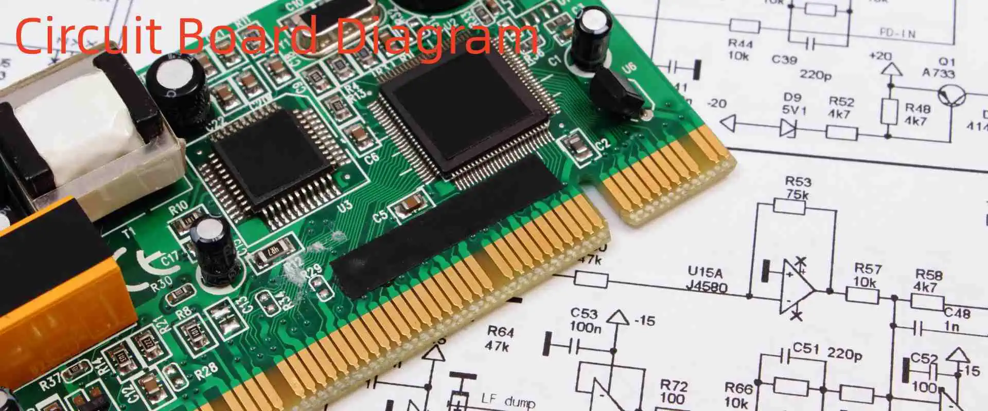
A circuit board schematic diagram is a graphical representation that shows the electrical connections and functions of components in an electronic circuit. It visualizes the structure of a circuit board by using symbols, lines and labels to define components and interconnections without necessarily representing physical dimensions or layout.
Schematics serve as an important reference for designing, building and troubleshooting circuit boards. Here is an in-depth look at schematic diagrams and their role in printed circuit board (PCB) development.
Contents
- Overview of Circuit Board Schematics
- Purpose and Advantages
- Symbols Used in Schematics
- Passive Components
- Active Components
- Integrated Circuits and Processors
- Connectors and Electromechanical Parts
- Representing Connections
- Identifying Schematic Elements
- Example Circuit Board Schematics
- Steps to Create a Schematic Diagram
- Schematic Capture and CAD Software
- Verifying Schematic Correctness
- Transition from Schematics to Board Layout
- Role in PCB Design Flow
- Applications and Usage
- Schematic Diagram vs PCB Layout
- FAQs
Overview of Circuit Board Schematics
A circuit schematic or schematic diagram comprises symbols, lines and text to show the connectivity and functions of electronic components that are part of a circuit. It is a graphical blueprint that defines the logical connections and relationships between components, without regard to exact physical placement on a PCB.
Schematics provide a simple visualization of a circuit using standardized representations for components and interconnections. This abstraction from physical form enables focus on how components logically connect and interact in an electrical network. Schematics can describe systems ranging from simple analog circuits to complex digital systems.
Schematic example showing symbols, connections and labels
Engineers create schematic diagrams to conceptualize circuit designs before actual implementation as PCBs. By using schematics, circuits can be simulated, analyzed, troubleshooted and optimized effectively at the design stage itself.
Schematics provide the starting point for translating circuit principles into physical PCB designs. They allow communication of design intent in an easy pictorial form for use during development and documentation.
Purpose and Advantages
Circuit schematics serve various important purposes:
- Visualize the overall structure and electrical connectivity in a circuit.
- Clarify the logical interactions between components.
- Act as preliminary design blueprints prior to PCB layout.
- Enable simulation of circuit behavior and performance analysis.
- Allow functional verification through CAD tools.
- Provide troubleshooting reference during testing and debug.
- Facilitate design reviews and project discussion.
- Document finished designs for manufacturing and support.
Key advantages of using schematic diagrams for circuit design include:
- Simplicity in depicting connections without layout constraints.
- Clarity in presenting circuit functionality.
- Flexibility to experiment with different configurations.
- Ease of design reuse by modifying existing schematics.
- Support for simulation through SPICE models.
- Cost-effective functional validation before prototyping.
- Intuitive visualization of overall system structure.
Symbols Used in Schematics
Schematics employ standardized symbols to represent the different components in a circuit. These symbols are graphic primitives that schematic editors and CAD software tools easily understand. The symbols follow various industry standards prescribed by organizations like IEEE, ANSI, IEC, JEDEC and CSA.
Some common categories of schematic symbols are:
Passive Components
- Resistor – Zigzag line
- Capacitor – Parallel lines
- Inductor – Coiled loops
- Transformer – Adjacent inductors with dotted line
- Crystal/Resonator – Angled lines between terminals
Standard symbols for passive components
Active Components
- Diode – Triangle with line
- LED – Triangle with extra line
- Zener diode – Z-shaped line
- Transistor – Three terminal discrete shape
- Vacuum tube – Circle with external connections
Symbols for active components
Integrated Circuits and Processors
- IC – Rectangle with pins
- Gate – Flat shape with pins
- Analog IC – Rectangle with added triangle
- Microcontroller – Rectangle with labels
- CPU – Rectangle with extra lines
Representation of ICs and processors
Connectors and Electromechanical Parts
- USB port
- D-sub connector
- Headers
- Test points
- Fuses
- Buttons and switches
- Relays
- Buzzers
- Battery symbols
Connectors, switches and other electromechanical symbols
Standardized schematic symbols for hundreds of electronic components are compiled in datasheets and reference material. Consistently following the prescribed representations is important for clear communication of the circuit structure.
Representing Connections
Schematics use lines to depict direct connections between component terminals or nodes in a circuit. The lines indicate how current flows when components interact. Some representations of connections in schematics are:
- Simple wires – Solid lines
- Crossed wires – No connection when crossing
- Joined wires – Branching connections
- Bus lines – Thick lines for node groups
Examples of schematic connection styles
Key points:
- Lines follow horizontal and vertical paths between component symbols.
- Wires terminate precisely at component terminations.
- Line intersections don’t imply connections unless joined by a node.
- Labels and net names clarify complex connections.
Such pictorial connectivity allows tracing individual paths and loops to understand overall circuit continuity.
Identifying Schematic Elements
Along with symbols and lines representing circuit elements, additional items are included in a schematic diagram for identification and documentation:
Component Designators
Alphanumeric labels like R1, C5, U3 that uniquely identify each component on the schematic.
Component Values
Resistance, capacitance and other parameter values that define component characteristics.
Net Names
Names representing common node points and connections like VCC, OUT, CLK. Helps identify signals.
Annotations
Supporting text providing details like component ratings and performance specs.
Boxes and Shapes
Contain groups of components or visualize functional blocks.
Sheet Numbers
Used on multi-page schematics to identify each sheet.
Legends and Notes
Supply additional circuit description and operational information.
Such labeling makes schematics self-documenting about components and connections in the circuit.
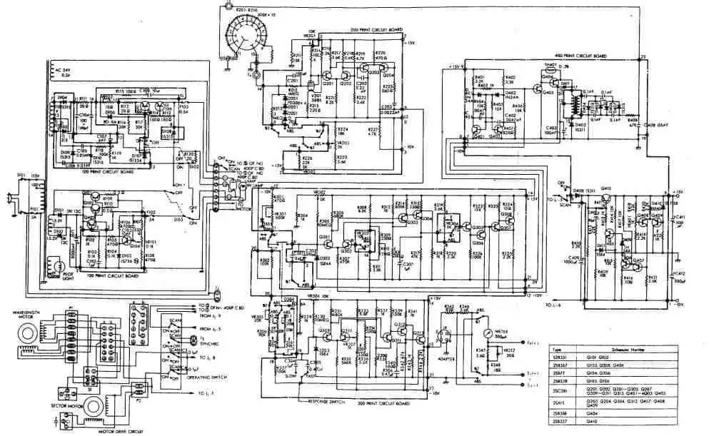
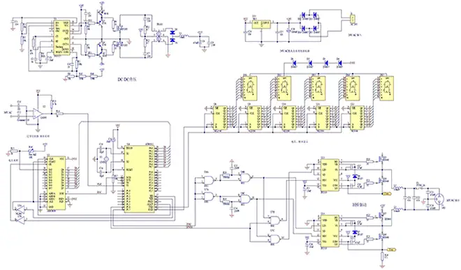
Example Circuit Board Schematics
Here are some examples of typical circuit schematics:
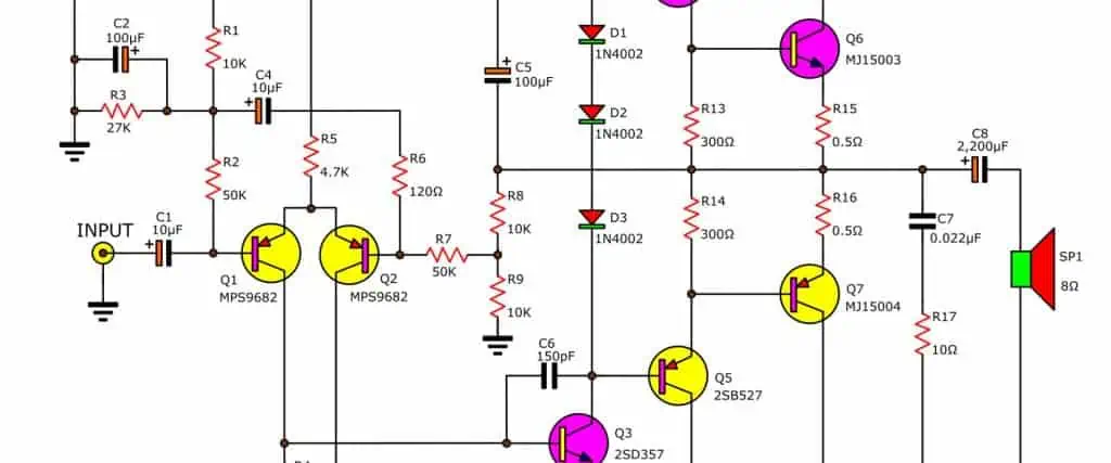
1. Voltage Regulator
Simple linear voltage regulator using transistors, resistors and capacitors. Note the standard symbols and net names.
2. 555 Timer Circuit
Shows a 555 timer IC chip providing output waveform using resistors and capacitors.
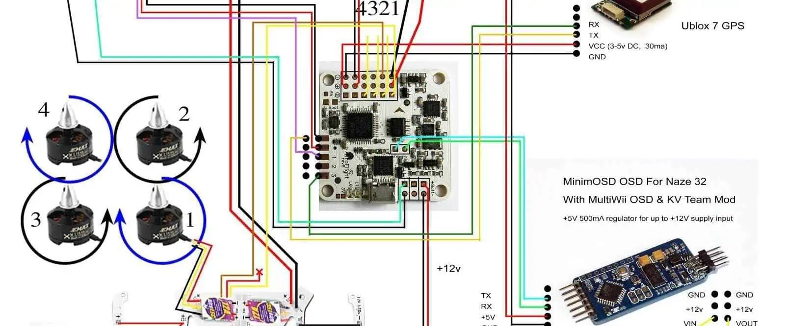
3. Microcontroller System
This schematic represents a microcontroller, its program memory, communication interfaces and discrete peripherals.
4. Switching Power Supply
Shows continuous output DC voltage derived from AC mains using diodes, switching ICs, inductors, transformers etc.
These examples illustrate the wide applicability of schematics for visualizing electronic circuits across domains.
Steps to Create a Schematic Diagram
Here is a typical workflow to systematically develop a circuit schematic diagram:
- Define Circuit Functionality – Study specifications and establish operating parameters.
- Research Components – Select suitable ICs, transistors, passive parts etc. based on specs.
- Create Component Symbols – Add required symbols to schematic component library.
- Arrange Symbols – Position and orient components based on functional blocks.
- Draw Connections – Connect component terminals as per electrical continuity.
- Label Components – Add unique designators and values for identification.
- Name Nets – Assign names to highlight power, ground, signals etc.
- Add Supporting Text – Include annotations, boxes, legends as required.
- Organize Sheets – Break up into logical sheets for multi-page designs.
- Verify Circuits – Validate schematic for correctness through simulation.
Executing these steps effectively results in accurate schematics that can be used for PCB design and verification.
Schematic Capture and CAD Software
Circuit schematic diagrams are created using specialized CAD software tools called schematic capture or schematic entry programs. These tools provide a graphical interface to efficiently generate circuit schematics along with built-inchecking and analysis features.
Key capabilities include:
- Drag-and-drop placement of component symbols from libraries
- Drawing connectivity and buses between component pins
- Auto-generation of designators and net names
- Electrical rule checking (ERC) to detect errors
- Annotation and documentation
- Circuit simulation linked to SPICE models
- Libraries of manufacturer component models
- Reporting schematic statistics like net count
- Integration with PCB layout workflow
Popular schematic capture software options are:
- Altium Designer
- Cadence OrCAD
- Mentor Graphics Xpedition
- Autodesk Eagle
- KiCad
- CadSoft EAGLE
- Zuken CR-8000
- PTC Creo Schematics
- Labcenter Proteus
Such tools help automate much of the schematic creation process and reduce errors.
Verifying Schematic Correctness
It is critical to validate schematics thoroughly before proceeding with PCB layout and fabrication. Some ways to verify schematic correctness are:
Visual Inspection
Scan schematic sheets manually to check for:
- Missing connections between component pins
- Un-terminated wires and ports
- Unlabeled components and nets
- Wrong component symbols used
- Multiple components mapped to the same designator
- Unrealistic parameter values assigned
Electrical Rules Check (ERC)
Use the CAD tool’s built-in ERC feature to automatically detect common errors like:
- Unconnected pins
- Missing power or ground connections
- Conflicting output/input connections
- Invalid component combinations
ERC confirms electrical validity based on user-defined rules for voltages, bidirectional pins, fanout limits etc.
Circuit Simulation
Simulate schematic behavior using integrated SPICE simulation tools to verify:
- Logical correctness of connections
- Expected voltages at circuit nodes
- Proper functioning for given parameter values
- Power dissipation, signal integrity etc. within limits
Design Reviews
Conduct peer reviews of schematics to get fresh perspectives in spotting discrepancies missed otherwise.
Using such validation checks helps avoiding propagation of faults into the PCB layout stage.
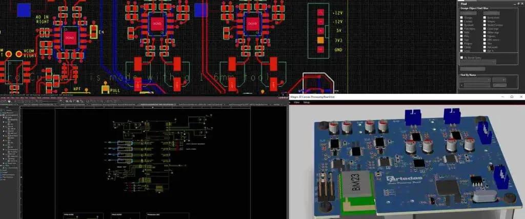
Transition from Schematics to Board Layout

After completing the schematic design capture and verification process, the next step is translating the logical connectivity into physical PCB layout.
Schematic capture tools allow forward annotation of the schematic to PCB layout software, enabling automated transfer of:
- Component symbols and footprints
- Netlist connectivity matrix
- Design rules and constraints
- Component libraries and properties
- Net names and attributes
This preserves the schematic’s design intent while providing the starting point for board layout. Component placement and routing can proceed based on the transferred netlist.
Bi-directional ECO changes between schematic and PCB design stages maintain synchronization. The schematic keeps providing the source of truth for layout modifications. Maintaining schematic-board congruity throughout the development cycle ensures correct PCB implementation.
Role in PCB Design Flow
Schematic capture is an integral stage of the overall printed circuit board design flow:
Typical PCB design flow highlighting schematic creation stage
- The process starts with the schematic entry phase where the logical electronic connections are established using CAD software.
- The connectivity information is then passed on to PCB layout for physical implementation.
- Feedback loops enable iterative improvements spanning schematic and layout cycles.
- Final design validation confirms schematic-to-layout correspondence.
The schematic thus serves as the foundation for realizing the physical incarnation of the electronic circuit and guides each downstream step.
Keeping the schematic updated and synchronized is essential for PCB design success.
Applications and Usage
Circuit schematic diagrams find ubiquitous application across multiple domains including:
Electronics Research
Schematics are used in papers and technical articles to explain circuit principles and innovations. They concisely present new concepts, measurements and results.
Circuit Design
Engineers create schematics to model electronic systems under development, before implementing them as PCBs. It is the starting point for prototyping.
Education and Learning
Schematics are used extensively in text books, reference designs and tutorials to teach circuit theory and practical electronics.
Troubleshooting and Repair
Technicians rely on product schematics to trace faults and debug issues during system maintenance and service.
Documentation
Finished schematics document the structure and operation of completed products, systems and infrastructure deployments.
Manufacturing
Production testing, assembly, integration and sustenance engineering functions depend on always-available schematics for manufacturing support.
Compliance
Schematics need to be provided as part of technical documentation for regulatory standards compliance in domains like medical, automotive, industrial etc.
IP Protection
Patent applications for innovative circuit designs require detailed schematics as part of the disclosure documents.
For each application, schematics provide unique value through clear visualization of circuit theory, connections, structure and operation.
Schematic Diagram vs PCB Layout

While the schematic diagram and PCB layout represent the same electronic circuit, they do so from different perspectives:
| Schematic Diagram | PCB Layout |
|---|---|
| Uses symbols and lines for connectivity | Uses component footprints and traces |
| Focuses on electrical functions | Focuses on physical implementation |
| Abstract representation | Geometrically accurate representation |
| Concerned with logics and signals | Concerned with placement and routing |
| Hierarchy based on circuit blocks | Hierarchy based on physical partitions |
| Emphasizes simplicity | Emphasizes manufacturability |
The schematic depicts electronic theory and principles. The layout realizes the schematic connections as an engineered product. Both are essential – the schematic provides the conceptual model while the PCB layout enables practical realization of the same design.
FAQs
Q1. Why are schematic diagrams essential?
Schematics provide a simple, visual representation of complex circuits using standardized symbols. This enables understanding the theoretical connectivity and interactions in an electronic system. Schematics are vital for conceptualizing and communicating circuit designs.
Q2. How are schematics useful for troubleshooting?
When debugging issues with PCBs and circuits, schematics help trace and isolate faults by clearly showing all connections and hidden nets. Techs can cross-verify circuits against the schematic to pinpoint discrepancies.
Q3. What makes a good schematic diagram?
Characteristics of a good schematic include – clarity, simplicity, legibility, completeness in connectivity, minimal crossings, well-defined symbols, proper annotations, consistency in presentation. This enhances comprehension.
Q4. How can schematics be verified before PCB design?
Schematics can be checked through methods like visual inspection, electrical rules check, circuit simulation, peer reviews and design validation tests to confirm completeness and correctness before progressing to layout.
Q5. Why is synchronizing schematics and PCB layout important?
Maintaining congruity between the schematics and PCB layout throughout the design process ensures the physical board correctly implements the logical schematic connections. This synchronization is critical for design success.
Summary
Circuit schematic diagrams provide a fundamental representation of electronic systems by depicting component connectivity and interactions using standardized symbols. Developing schematics