Application of CAN XL Communication Technology in Automotive Millimeter-Wave Radar: A Comprehensive Analysis

Introduction

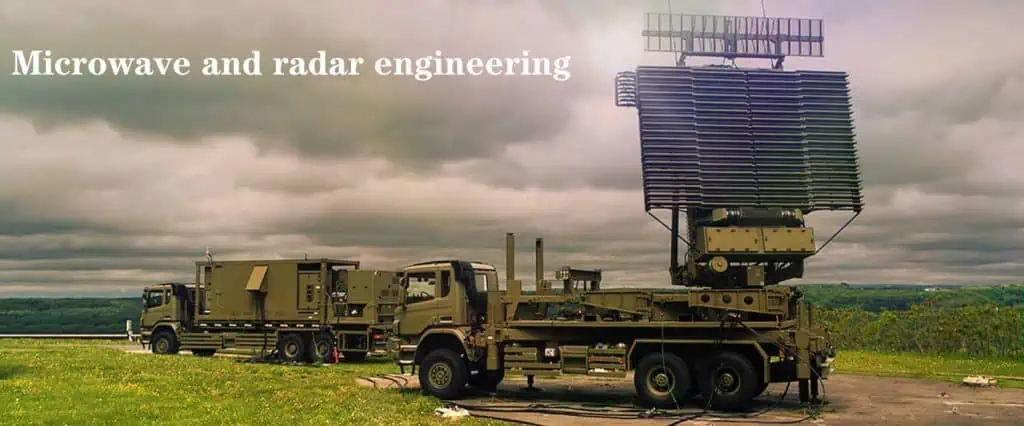
The automotive industry stands at the precipice of a revolutionary transformation, driven by the relentless pursuit of safer, smarter, and more autonomous mobility solutions. At the heart of this evolution lies sensing technology, which serves as the digital nervous system of modern vehicles. Among the constellation of sensors that enable advanced driver assistance systems (ADAS) and autonomous driving capabilities, automotive millimeter-wave radar has emerged as a cornerstone technology, increasingly favored by Original Equipment Manufacturers (OEMs) worldwide.

The preference for millimeter-wave radar stems from its exceptional reliability, precision, and robust performance across diverse environmental conditions. Unlike optical sensors that struggle in adverse weather, radar systems maintain consistent operation regardless of lighting conditions, precipitation, or atmospheric visibility. This reliability makes them indispensable for safety-critical applications where consistent performance can mean the difference between accident avoidance and catastrophic failure.

However, as ADAS systems evolve toward greater sophistication and autonomous driving capabilities advance, the data throughput requirements from radar sensors have grown exponentially. Traditional communication protocols, while adequate for earlier generations of automotive electronics, are increasingly strained by the bandwidth demands of modern radar systems. This challenge has catalyzed the development and adoption of CAN XL (Controller Area Network eXtended Length), a next-generation communication protocol that promises to bridge the gap between current capabilities and future requirements.

This comprehensive analysis explores the technical advantages of CAN XL over traditional CAN FD (CAN with Flexible Data-Rate) communication technology specifically in millimeter-wave radar applications, examining not only the immediate benefits but also the long-term implications for automotive system architecture and performance optimization.

1. Technical Advantages and Evolution of Millimeter-Wave Radar

The Multi-Sensor Ecosystem

Contemporary ADAS implementations represent sophisticated multi-sensor ecosystems, integrating cameras for visual perception, LiDAR for high-resolution 3D mapping, ultrasonic sensors for close-proximity detection, and millimeter-wave radar for robust all-weather sensing. Each sensor type contributes unique capabilities to the overall perception system, but millimeter-wave radar occupies a particularly crucial niche due to its distinctive operational characteristics.

Unparalleled All-Weather Reliability

The fundamental physics underlying millimeter-wave radar operation provides inherent advantages in challenging environmental conditions. Operating in the 77 GHz frequency band, these systems transmit electromagnetic waves that exhibit minimal attenuation when traversing atmospheric moisture, dust particles, or other environmental obstacles that severely degrade optical sensors. Unlike cameras, which become virtually useless in dense fog or heavy precipitation, or LiDAR systems that suffer significant range reduction in adverse weather, millimeter-wave radar maintains consistent detection capabilities across the full spectrum of weather conditions encountered in real-world driving scenarios.

This reliability extends beyond mere functionality to encompass consistent performance characteristics. While camera-based systems may experience varying levels of degradation depending on the severity of weather conditions, radar systems maintain stable detection ranges, resolution, and accuracy regardless of environmental factors. This predictable performance is crucial for safety-critical applications where system behavior must be deterministic and reliable.

Enhanced Detection Capabilities and Resolution

The evolution to 77 GHz millimeter-wave radar represents a significant advancement over earlier 24 GHz systems. The higher frequency enables substantially improved angular resolution, allowing for more precise object localization and enhanced ability to distinguish between closely spaced targets. This improved resolution translates directly into better object classification capabilities, enabling systems to differentiate between pedestrians, cyclists, vehicles, and stationary objects with greater accuracy.

The extended detection range capabilities of modern 77 GHz systems enable earlier threat detection and longer decision-making windows for autonomous systems. Long-range detection is particularly crucial for highway applications, where high-speed scenarios require maximum advance warning to execute safe maneuvers. Current generation systems can reliably detect and track objects at distances exceeding 200 meters, providing sufficient time for complex decision-making processes in high-speed scenarios.

Superior Penetration and Environmental Adaptability

Beyond weather immunity, millimeter-wave radar demonstrates remarkable penetration capabilities that extend its utility beyond conventional sensing applications. The ability to detect objects through fog, dust, smoke, and even certain solid materials provides unique advantages in complex driving environments. For instance, radar can detect vehicles obscured by dust clouds on unpaved roads, or identify obstacles through light vegetation that would completely block optical sensors.

This penetration capability also enables innovative applications such as through-bumper mounting, where radar sensors can be completely hidden behind vehicle body panels without performance degradation. This integration flexibility allows automotive designers to maintain aesthetic integrity while providing comprehensive sensor coverage.

Economic and Practical Considerations

From a practical deployment perspective, millimeter-wave radar offers compelling economic advantages compared to alternative sensing technologies. While LiDAR systems currently command premium prices that limit their deployment to luxury vehicles, millimeter-wave radar achieves an optimal balance between cost and performance that makes it viable for mass-market applications. The manufacturing processes for radar sensors have matured significantly, enabling economies of scale that further enhance their cost-effectiveness.

Additionally, the robust nature of radar sensors reduces maintenance requirements and extends operational lifespans compared to more delicate optical systems. This reliability translates into lower total cost of ownership and improved customer satisfaction through reduced service interventions.

2. The Data Revolution: Understanding Radar Output Growth

Data Generation and Structure

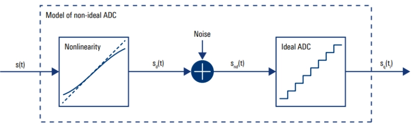
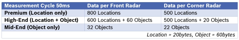
Modern millimeter-wave radar systems generate sophisticated real-time data streams that provide comprehensive environmental perception capabilities. These systems typically output data in two primary formats: point clouds that represent raw detection data, and object lists that contain processed information about tracked targets. Each format serves specific purposes within the broader ADAS architecture and places distinct demands on communication infrastructure.

Point cloud data represents the fundamental output of radar signal processing, containing individual detection points with associated metadata including range, relative velocity, angle of arrival, and signal strength information. A single radar sensor can generate hundreds to thousands of these detection points per measurement cycle, with typical refresh rates of 50 milliseconds ensuring real-time environmental updates.

Object list data represents a higher level of processing, where individual detection points are clustered, tracked, and classified into discrete objects. Each object entry contains comprehensive information including position coordinates, velocity vectors, acceleration estimates, object dimensions, classification confidence levels, and unique tracking identifiers that enable consistent object following across multiple measurement cycles.

Factors Driving Bandwidth Growth

The exponential growth in radar data output stems from multiple converging trends in automotive technology development. Advanced ADAS implementations increasingly require finer-grained object detection and classification capabilities to make sophisticated driving decisions. Where earlier systems might simply detect the presence of an object, modern implementations must distinguish between pedestrians, cyclists, motorcycles, passenger cars, commercial vehicles, and various types of roadside infrastructure.

This enhanced classification capability necessitates more detailed radar signatures, requiring higher resolution data and more sophisticated processing algorithms. The resulting data volume growth places increasing strain on communication systems that were designed for earlier generations of sensors with more modest bandwidth requirements.

Furthermore, the trend toward faster safety response times drives the need for higher-frequency data updates. Critical safety functions such as Automatic Emergency Braking (AEB), Pedestrian Collision Warning (PCW), and Lane Departure Warning (LDW) systems require minimal latency between threat detection and response activation. Achieving these response times requires not only faster sensor processing but also higher-speed communication links to minimize data transmission delays.

Next-Generation Radar Technologies

The emergence of 4D imaging radar technology represents the next evolutionary step in automotive radar development. Unlike conventional radar systems that provide range, velocity, and azimuth information, 4D systems add elevation detection capabilities, creating comprehensive three-dimensional environmental maps with velocity information for each detected point. This additional dimension significantly increases data volume while providing enhanced object classification and environmental understanding capabilities.

The integration of artificial intelligence and machine learning algorithms into radar processing systems further amplifies data requirements. AI-driven sensor fusion systems require access to raw or minimally processed sensor data to optimize environmental perception models. These systems consume substantially more bandwidth than traditional rule-based processing approaches but offer significantly enhanced performance in complex scenarios.

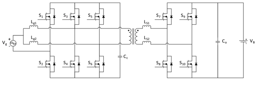
3. CAN XL: The Next Generation Communication Solution

Evolution of CAN Technology

The Controller Area Network (CAN) protocol has served as the backbone of automotive communication systems for decades, evolving through multiple generations to meet changing industry requirements. The progression from Classic CAN through CAN FD to CAN XL represents a continuous refinement process, with each generation addressing specific limitations while maintaining backward compatibility and preserving the fundamental strengths that made CAN successful in automotive applications.

CAN XL represents the third generation of this evolutionary process, incorporating lessons learned from previous implementations while addressing the specific challenges posed by modern high-bandwidth applications. The protocol maintains the robust error handling, deterministic behavior, and cost-effective implementation characteristics that made its predecessors successful while dramatically expanding performance capabilities.

Technical Innovations in CAN XL

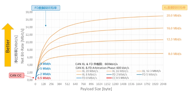
The most significant advancement in CAN XL is the expansion of maximum payload size from the 64-byte limit of CAN FD to 2048 bytes per frame. This eight-fold increase in payload capacity fundamentally changes the efficiency characteristics of data transmission, particularly for applications that generate large data blocks such as radar point clouds or compressed sensor data.

Beyond payload expansion, CAN XL incorporates enhanced security features designed to address the growing cybersecurity concerns in connected vehicles. These security enhancements include improved error detection mechanisms, enhanced frame authentication capabilities, and provisions for encryption integration that help protect critical vehicle systems from malicious attacks.

The protocol also introduces functional safety improvements that align with the stringent reliability requirements of ADAS applications. Enhanced fault detection and isolation capabilities ensure that communication errors are quickly identified and contained, preventing the propagation of corrupted data that could compromise safety-critical decision-making processes.

Architectural Flexibility and Implementation Options

CAN XL provides unprecedented architectural flexibility through its support for mixed-network implementations. Systems can combine CAN FD and CAN XL nodes within the same network, operating at speeds up to 8 Mbit/s while maintaining full compatibility. This capability enables automotive manufacturers to implement gradual migration strategies, upgrading high-bandwidth nodes to CAN XL while maintaining existing CAN FD infrastructure for lower-bandwidth applications.

For applications requiring maximum performance, pure CAN XL networks can achieve communication speeds up to 20 Mbit/s, providing substantial bandwidth increases over previous generation protocols. This high-speed capability is particularly valuable for applications such as radar sensor networks where multiple high-bandwidth sensors must share common communication infrastructure.

4. Performance Analysis: CAN FD vs. CAN XL

Quantitative Performance Comparisons

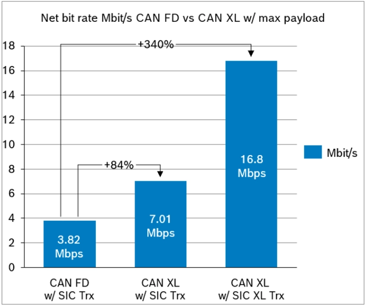
Comprehensive analysis of communication efficiency reveals substantial advantages for CAN XL implementations across multiple performance metrics. When comparing systems operating at equivalent 8 Mbit/s speeds, CAN XL achieves 84% higher net bitrate compared to CAN FD implementations using CAN SIC transceivers. This improvement stems primarily from the increased payload efficiency enabled by larger frame sizes, which amortize protocol overhead across more user data.

The performance advantage becomes even more pronounced when leveraging CAN XL’s maximum speed capabilities. Comparing CAN XL at 20 Mbit/s against CAN FD at 8 Mbit/s reveals a 340% increase in net bitrate, representing a transformational improvement in communication capacity. This dramatic performance increase enables entirely new classes of applications that would be impossible with previous generation protocols.

Practical Implications for Radar Applications

These performance improvements translate directly into enhanced radar system capabilities and improved overall vehicle performance. Higher bandwidth availability enables radar sensors to transmit more detailed environmental data, supporting enhanced object classification and tracking capabilities. The reduced latency achievable with higher-speed communication also enables faster safety response times, directly improving vehicle safety performance.

The increased bandwidth also provides headroom for future capability expansion without requiring communication system redesign. As radar sensors continue to evolve toward higher resolution and more sophisticated processing capabilities, CAN XL provides the communication infrastructure necessary to support these advances.

5. System Architecture Analysis: Five-Radar Implementation Scenarios

Premium and High-End Vehicle Configurations

Premium and high-end vehicle implementations typically deploy five millimeter-wave radar sensors in a comprehensive coverage pattern, including one forward-looking long-range radar and four corner-mounted medium-range radars providing 360-degree environmental awareness. These configurations generate substantial data volumes that challenge traditional communication architectures.

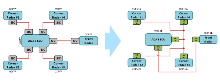
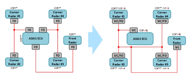
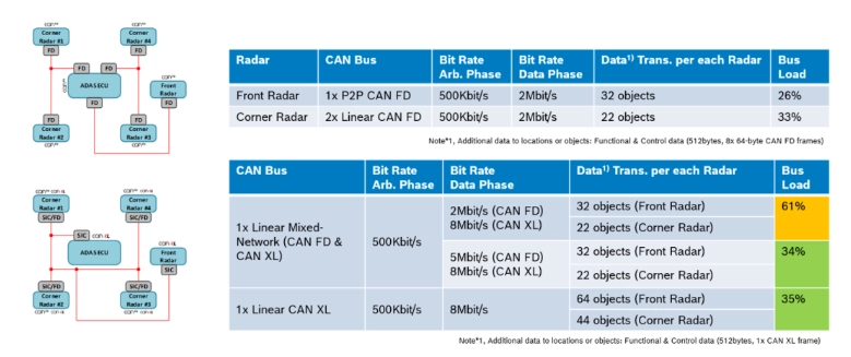
Current CAN FD implementations for these scenarios typically require five point-to-point communication buses, one dedicated to each radar sensor. Operating at 5 Mbit/s, these implementations experience bus loading levels exceeding 50%, with some configurations reaching 87% capacity utilization. Such high loading levels are impractical for production deployment due to insufficient margin for data volume growth and potential timing violations under peak loading conditions.

CAN XL enables dramatic architectural simplification and performance improvement for these demanding applications. A two-bus architecture utilizing one point-to-point connection for the front radar and one linear bus serving all four corner radars can handle equivalent data loads at only 40% capacity utilization when operating at 20 Mbit/s. This configuration provides substantial headroom for future capability expansion while reducing system complexity.

The economic benefits of CAN XL implementation in premium scenarios are substantial. Reducing the number of required communication buses from five to two decreases external component requirements by approximately 60%, including reductions in transceiver quantities, electromagnetic compatibility (EMC) filters, connectors, and associated wiring harnesses. These component savings translate directly into reduced manufacturing costs and simplified assembly processes.

Mid-End Vehicle Optimizations

Mid-end vehicle implementations present different optimization opportunities where mixed-network approaches can provide incremental improvements while maintaining cost competitiveness. These scenarios typically begin with three-bus CAN FD architectures and can benefit from selective CAN XL upgrades that provide performance improvements without requiring complete system redesign.

Mixed CAN FD and CAN XL implementations operating at 2 Mbit/s and 8 Mbit/s respectively can achieve significant bus load reductions while maintaining compatibility with existing system components. Further optimization through speed increases to 5 Mbit/s CAN FD and 8 Mbit/s CAN XL can achieve 34% bus loading, providing excellent performance margins.

Full CAN XL implementations at 8 Mbit/s maintain 35% bus loading even with doubled data volume, providing substantial growth capability for future feature additions. This headroom is crucial for mid-market vehicles where feature content continues to expand but cost pressures remain significant.

Conclusion and Future Outlook

The analysis presented demonstrates compelling advantages for CAN XL implementation in automotive millimeter-wave radar applications. The combination of dramatically increased payload capacity, enhanced communication speeds, and architectural flexibility positions CAN XL as the optimal communication solution for current and future radar system requirements.

As millimeter-wave radar technology continues advancing toward higher resolution, enhanced object classification, and integration with artificial intelligence processing systems, the bandwidth requirements will continue growing exponentially. CAN XL provides the communication infrastructure necessary to support these advances while maintaining the cost-effectiveness and reliability that automotive applications demand.

The transition to CAN XL represents more than a simple protocol upgrade; it enables entirely new classes of automotive applications and capabilities that were previously impossible due to communication bandwidth limitations. As the technology matures and achieves widespread adoption, CAN XL is positioned to become the standard communication interface for next-generation ADAS implementations, supporting the industry’s continued evolution toward fully autonomous mobility solutions.

Understanding and Mitigating IGBT Short-Circuit Oscillations: A Comprehensive Analysis

Introduction

Insulated Gate Bipolar Transistors (IGBTs) have become indispensable components in modern industrial applications, ranging from sophisticated motor drive systems to advanced electrical control circuits. These semiconductor devices are particularly valued for their ability to achieve significantly lower switching losses compared to conventional alternatives, making them essential for energy-efficient power electronics. However, the operational reliability of IGBTs extends beyond their switching performance to include their ability to withstand fault conditions, particularly short-circuit events.

During normal operation, IGBTs must demonstrate robust short-circuit withstand capability to ensure system reliability and safety. However, when short-circuit oscillations (SCOs) occur during fault conditions, the IGBT’s ability to survive these events can be severely compromised. These oscillations not only threaten the device’s structural integrity but can also generate electromagnetic interference (EMI) hazards when the oscillation amplitude becomes excessive and the collector-emitter voltage (VCE) range spans too broadly. Consequently, understanding and optimizing SCO behavior under short-circuit conditions has become a critical aspect of IGBT design and application.

Fundamental Mechanisms of Short-Circuit Oscillations

The root cause of short-circuit oscillations in IGBTs lies in the complex interplay between charge carrier dynamics and electric field distributions within the device structure. Unlike conventional design parameters that affect basic IGBT characteristics, SCO behavior is primarily influenced by the backside design elements, specifically the Field Stop (FS) layer and P+ emitter configurations. These structural components directly impact the bipolar current gain coefficient (ฮฑpnp) of the IGBT’s inherent pnp transistor, which plays a pivotal role in determining oscillation characteristics.

To understand this phenomenon, consider the IGBT structure under steady-state conditions at a constant junction temperature. When examining the output characteristics at different collector-emitter voltages (300V and 500V), distinct regions emerge within the device: the quasi-plasma region, the space charge region, and the plasma region. The vertical distribution of electric field intensity and carrier density reveals that high electric field intensity in the FS region results from negative space charges accumulated in the drift region.

The oscillation mechanism becomes apparent when analyzing transient behavior during short-circuit conditions. The periodic storage and release of charge carriers within the device, combined with corresponding variations in electric field distribution, creates the characteristic high-frequency oscillations observed in short-circuit conditions. This phenomenon manifests as electrons and holes being alternately stored within the device structure and then released in surge-like formations that propagate through different regions of the IGBT.

During the initial phase of oscillation, charge carriers accumulate primarily in the internal regions of the device. As the oscillation progresses, a charge-carrier plasma surge gradually forms and begins propagating through the device structure. This surge eventually reaches the FS region, where it triggers the release of stored electrons and holes. The cyclical nature of this storage and release process, coupled with the dynamic electric field redistribution, sustains the oscillation behavior and determines its frequency characteristics.

Impact of Device Structure on Oscillation Behavior

P+ Emitter Dose Effects

The concentration of dopants in the P+ emitter region significantly influences the IGBT’s short-circuit oscillation characteristics. Experimental analysis reveals that the emitter dose effect on hole injection and the bipolar current gain coefficient (ฮฑpnp) is most pronounced at collector-emitter voltages below 250V. This voltage range corresponds to the region where SCOs typically initiate and are most problematic.

When the P+ emitter dose is increased, several important changes occur in the device’s internal structure and behavior. The remaining plasma region located in front of the P+ emitter expands, and its maximum carrier density level increases correspondingly. This enhancement in plasma characteristics leads to a slight increase in electric field intensity within the drift region preceding the FS layer, while simultaneously causing a slight reduction in field intensity within the FS layer itself.

The relationship between P+ emitter dose and oscillation behavior follows a predictable pattern: as the emitter dose increases, the bipolar current gain coefficient (ฮฑpnp) also increases. This increase in ฮฑpnp correlates directly with a reduction in both the voltage range over which SCOs occur and the amplitude of the oscillations themselves. This relationship suggests that optimizing the P+ emitter dose can be an effective strategy for mitigating problematic oscillation behavior.

FS Layer Dose Optimization

The Field Stop layer dose represents another critical parameter in controlling short-circuit oscillations. For collector-emitter voltages exceeding 50V, the FS layer dose demonstrates significant influence over hole injection characteristics and the resulting ฮฑpnp values. This influence extends across a broader voltage range compared to the P+ emitter dose effects, making FS layer optimization particularly important for comprehensive oscillation control.

Reducing the FS layer dose produces notable changes in the device’s internal carrier distribution. The plasma region positioned in front of the P+ emitter contracts, leading to alterations in the overall charge carrier dynamics. These changes manifest as modifications in both the voltage range where SCOs occur and their amplitude characteristics.

Interestingly, as the FS layer dose decreases and ฮฑpnp increases, the voltage range where SCOs occur shifts toward lower voltages. However, this shift is accompanied by beneficial reductions in both the overall voltage range affected by oscillations and the amplitude of the oscillations themselves. This behavior indicates that FS layer dose optimization can provide a pathway for minimizing oscillation-related problems while potentially shifting their occurrence to less critical operating conditions.

Temperature Dependencies and Thermal Effects

Junction temperature plays a multifaceted role in determining short-circuit oscillation behavior, affecting both hole current and channel current characteristics simultaneously. Temperature variations create complex changes in the device’s internal physics, influencing carrier mobility, injection efficiency, and field distribution patterns.

As junction temperature increases, the plasma region in front of the P+ emitter undergoes contraction, leading to modified charge carrier dynamics throughout the device structure. This thermal effect on plasma distribution directly impacts the oscillation characteristics, generally leading to reductions in both the voltage range affected by SCOs and their amplitude.

The temperature dependence of ฮฑpnp reveals additional complexity in the thermal behavior of SCOs. At lower collector-emitter voltages, ฮฑpnp decreases as junction temperature rises, likely due to reduced carrier mobility at elevated temperatures. This temperature-mobility relationship creates a natural suppression mechanism for oscillations at higher operating temperatures, suggesting that thermal management strategies could be incorporated into oscillation mitigation approaches.

Optimization Strategies and Design Trade-offs

Backside Design Approaches

Effective mitigation of short-circuit oscillations requires careful attention to backside design parameters, particularly those affecting the bipolar current gain coefficient under short-circuit conditions. The primary strategy involves increasing ฮฑpnp to levels sufficient for oscillation suppression or elimination. When ฮฑpnp reaches appropriately high values, SCOs can be completely avoided, providing a definitive solution to oscillation-related problems.

However, this optimization approach introduces important design trade-offs that must be carefully considered. Increasing ฮฑpnp to suppress oscillations inevitably leads to higher leakage currents during normal operation, which can impact device efficiency and power consumption. Additionally, turn-off losses increase, potentially offsetting some of the switching advantages that make IGBTs attractive for many applications.

Thermal Stability Considerations

Perhaps most critically, enhancing ฮฑpnp to eliminate SCOs can compromise thermal short-circuit stability, creating a complex optimization challenge. Device designers must balance oscillation suppression against thermal performance, leakage characteristics, and switching losses to achieve optimal overall performance.

This multifaceted trade-off requires comprehensive analysis of the specific application requirements and operating conditions. For applications where SCO suppression is paramount, accepting increased leakage and switching losses may be justified. Conversely, for applications where thermal performance and efficiency are critical, alternative approaches to oscillation management may be necessary.

Advanced Analysis and Future Directions

The relationship between oscillation amplitude and voltage range provides insights into the underlying physics governing SCO behavior. The peak-to-peak collector current amplitude serves as a quantitative measure of oscillation intensity, enabling systematic comparison of different design approaches and parameter optimization strategies.

Detailed analysis of carrier density distributions at various time points during oscillation cycles reveals the dynamic nature of charge carrier movement and storage within the device. These distributions demonstrate how carrier surges propagate through different device regions and how the timing of these movements influences overall oscillation characteristics.

Conclusion

Short-circuit oscillations in IGBTs represent a complex phenomenon requiring careful analysis of multiple interdependent factors. The periodic storage and release of charge carriers, driven by dynamic electric field distributions, creates the fundamental mechanism underlying these oscillations. Through systematic optimization of backside design parameters, particularly P+ emitter dose and FS layer dose, significant improvements in SCO behavior can be achieved.

The key to successful oscillation mitigation lies in understanding the role of the bipolar current gain coefficient (ฮฑpnp) and implementing design strategies that increase this parameter to appropriate levels. However, the inevitable trade-offs between oscillation suppression and other device characteristics necessitate careful consideration of specific application requirements.

Temperature effects provide both challenges and opportunities for oscillation management, with higher junction temperatures naturally suppressing SCO behavior. This thermal dependence suggests that integrated approaches combining structural optimization with thermal management could provide comprehensive solutions to oscillation-related problems.

Future developments in IGBT design will likely focus on advanced modeling techniques that can predict SCO behavior more accurately and enable optimization strategies that minimize the trade-offs inherent in current approaches. Understanding these complex interactions remains essential for continued advancement in power semiconductor technology and the development of more robust, efficient IGBT devices for demanding industrial applications.

What Exactly is the Difference Between Microwave Circuits and RF Circuits?

In the realm of high-frequency electronic engineering, two distinct yet related domains stand out: radio frequency (RF) circuits and microwave circuits. While both operate within the electromagnetic spectrum and share fundamental principles of electronics, they represent fundamentally different approaches to circuit design, analysis, and implementation. Understanding these differences is crucial for engineers working in telecommunications, radar systems, wireless communications, and countless other modern electronic applications.

Frequency Range: The Foundation of Distinction

The most fundamental distinction between RF and microwave circuits lies in their operating frequency ranges, which directly influences every other aspect of their design and implementation. RF circuits typically operate within the frequency band of 3 kHz to 300 MHz, encompassing everything from audio frequencies used in AM radio broadcasting to VHF communications used in television and two-way radio systems. This broad range includes various sub-bands such as low frequency (LF), medium frequency (MF), high frequency (HF), very high frequency (VHF), and the lower portion of ultra-high frequency (UHF).

Microwave circuits, on the other hand, operate in the significantly higher frequency range of 300 MHz to 300 GHz. This spectrum includes the upper UHF band, super high frequency (SHF), and extremely high frequency (EHF) ranges. In practical engineering applications, there exists a transitional zone between 300 MHz and 1 GHz where both RF and microwave design principles may apply, depending on the specific circuit dimensions and performance requirements.

The significance of this frequency distinction extends far beyond mere classification. At these different frequency ranges, the physical behavior of electromagnetic waves changes dramatically relative to typical circuit dimensions. When signal wavelengths become comparable to or smaller than the physical dimensions of circuit components, transmission lines, or interconnections, the electromagnetic wave nature of signals becomes the dominant design consideration rather than simple voltage and current relationships.

Design Philosophy: Lumped vs. Distributed Parameters

The transition from RF to microwave frequencies represents a fundamental shift in design philosophy, moving from lumped parameter models to distributed parameter approaches. This change reflects the underlying physics of electromagnetic wave propagation and has profound implications for circuit analysis and design methodologies.

RF Circuit Design Approach

In RF circuits, the signal wavelength is typically much larger than the physical dimensions of circuit components and interconnections. For instance, at 100 MHz, the free-space wavelength is approximately 3 meters, making most circuit elements electrically small. This allows engineers to employ lumped parameter models, where passive components such as resistors (R), capacitors (C), and inductors (L) are treated as ideal, concentrated elements with well-defined values.

Under the lumped parameter assumption, circuit analysis relies heavily on traditional network theory, Kirchhoff’s laws, and conventional AC circuit analysis techniques. The primary design concerns in RF circuits include signal modulation and demodulation, noise figure optimization, power amplification efficiency, and bandwidth considerations. Engineers focus on component selection, biasing schemes, and impedance matching using discrete components or simple transmission line segments.

RF circuit design emphasizes the careful management of parasitic effects that become more pronounced at higher frequencies within the RF range. Parasitic capacitances between traces, lead inductances, and skin effect losses all require attention, but they can generally be modeled using equivalent circuit approaches with additional lumped elements.

Microwave Circuit Design Approach

Microwave circuits operate in a fundamentally different regime where signal wavelengths approach or become smaller than circuit dimensions. At 1 GHz, the free-space wavelength is 30 cm, while at 10 GHz, it reduces to 3 cm. When dealing with printed circuit board (PCB) traces, component packages, or waveguide structures of comparable dimensions, the lumped parameter approximation breaks down completely.

Instead, microwave circuit design relies on distributed parameter models that account for the wave nature of electromagnetic propagation. Every transmission line segment, interconnection, and even component mounting becomes a distributed element characterized by its electromagnetic field patterns, characteristic impedance, and propagation characteristics.

The design process shifts from component-centric thinking to field-theory-based analysis. Engineers must consider transmission line theory, S-parameters, Smith chart analysis, and electromagnetic field distributions. The concept of electrical length becomes crucial, as a physically short connection might represent multiple wavelengths at microwave frequencies, creating complex resonant behaviors and phase relationships.

Impedance Matching: From Simple to Sophisticated

pcb impedance control

Impedance matching represents one of the most critical aspects where RF and microwave circuits diverge significantly in complexity and approach. While both domains require careful impedance considerations, the methods and criticality levels differ substantially.

RF Impedance Matching

In RF circuits, impedance matching primarily focuses on maximizing power transfer and minimizing signal reflections using relatively straightforward techniques. Engineers typically employ L-section, ฯ€-section, or T-section matching networks composed of lumped capacitors and inductors. The Smith chart may be used, but often simplified impedance calculations suffice for many applications.

The consequences of imperfect matching in RF circuits, while undesirable, are often manageable through design margins and can sometimes be compensated by increased amplifier gain or improved filtering. Return loss requirements are typically less stringent, with values of -10 dB to -15 dB often considered acceptable for many applications.

Microwave Impedance Matching

Microwave circuits demand far more sophisticated impedance matching approaches due to the distributed nature of the system and the higher frequencies involved. The reflection coefficient (ฮ“) becomes a critical design parameter, defined by:

ฮ“ = (Z_L – Z_0) / (Z_L + Z_0)

Where Z_L represents the load impedance and Z_0 represents the characteristic impedance of the transmission line system. Even small impedance mismatches can create significant signal reflections, leading to standing wave patterns that cause power loss, signal distortion, and potentially damaging voltage and current peaks.

Microwave matching networks often employ distributed elements such as quarter-wave transformers, stub tuners, and complex multi-section matching structures. Advanced techniques include the use of microstrip lines, striplines, coaxial structures, and waveguide components. The Smith chart becomes an indispensable tool for visualizing complex impedance transformations and designing matching networks.

The precision required in microwave impedance matching is significantly higher, with return loss requirements often exceeding -20 dB or -30 dB. This level of precision demands careful consideration of manufacturing tolerances, temperature stability, and frequency variations across the operating band.

Component Technologies and Material Considerations

The choice of components and materials represents another major distinction between RF and microwave circuit design, driven by the different physical phenomena dominant at each frequency range.

RF Circuit Components

RF circuits commonly utilize conventional semiconductor devices such as bipolar junction transistors (BJTs), metal-oxide-semiconductor field-effect transistors (MOSFETs), and junction field-effect transistors (JFETs). These devices can provide adequate performance at RF frequencies, with careful attention to parasitic effects and package considerations.

Passive components in RF circuits include wire-wound inductors, ceramic or film capacitors, and carbon or metal film resistors. While parasitic effects must be considered, these components can often provide satisfactory performance when properly selected and applied.

LC filter networks remain viable options for many RF applications, although engineers must account for the Q-factor limitations and parasitic resonances that become more prominent at higher RF frequencies.

Microwave Circuit Components

Microwave circuits require specialized semiconductor technologies optimized for high-frequency operation. High-electron-mobility transistors (HEMTs), particularly those fabricated using gallium arsenide (GaAs) or gallium nitride (GaN) technologies, offer superior performance at microwave frequencies. These devices provide higher gain, better noise figures, and improved linearity compared to conventional silicon-based transistors.

The transition to microwave frequencies often necessitates the abandonment of conventional lumped components in favor of distributed structures. Microstrip lines, striplines, and coplanar waveguides replace discrete inductors and capacitors. Resonant cavities, dielectric resonators, and surface acoustic wave (SAW) devices provide filtering functions with higher Q-factors and better temperature stability than possible with conventional LC networks.

Material selection becomes critically important in microwave circuits, with low-loss dielectric materials such as polytetrafluoroethylene (PTFE), Rogers RO4000 series laminates, or specialized ceramics preferred for substrates. Conductor materials must exhibit low surface roughness and high conductivity to minimize losses due to skin effect and surface current distribution.

Loss Mechanisms and Performance Limitations

The dominant loss mechanisms in RF and microwave circuits reflect the different physical phenomena at work in each frequency regime, requiring distinct approaches to loss minimization and performance optimization.

RF Circuit Losses

RF circuits primarily contend with conductor losses due to the finite resistance of metallic conductors and the skin effect that concentrates current flow near conductor surfaces. As frequency increases within the RF range, skin depth decreases, effectively reducing the cross-sectional area available for current flow and increasing resistance.

Device noise represents another significant concern in RF circuits, particularly in receiver front-end applications where low noise figures are essential for maintaining system sensitivity. Thermal noise, shot noise, and flicker noise all contribute to the overall noise performance, with careful device selection and circuit topology optimization required to achieve optimal performance.

Dielectric losses in RF circuits, while present, are typically less critical than at microwave frequencies due to the lower operating frequencies and the use of materials with adequate loss tangent characteristics for RF applications.

Microwave Circuit Losses

Microwave circuits must address a more complex set of loss mechanisms that become increasingly significant at higher frequencies. In addition to enhanced conductor losses due to increased current crowding and skin effect, dielectric losses become a major concern.

Dielectric loss occurs when electromagnetic energy is absorbed by insulating materials, converting it to heat. The loss tangent (tan ฮด) of substrate materials becomes a critical parameter, as even small values can result in significant signal attenuation over the distributed structures common in microwave circuits. This necessitates the use of specialized low-loss materials and careful attention to substrate thickness and uniformity.

Radiation losses represent another unique challenge in microwave circuits, occurring when electromagnetic energy escapes from transmission lines or circuit structures and propagates into free space. This is particularly problematic in open structures such as microstrip lines, where fringing fields can couple to nearby conductors or radiate energy away from the intended signal path.

To combat radiation losses, microwave circuits often incorporate shielding structures, ground plane designs, and via fencing to contain electromagnetic fields within the intended circuit boundaries. The design of these structures requires careful electromagnetic simulation and optimization to achieve the desired performance while maintaining manufacturing feasibility.

Application Domains and System Requirements

The distinct characteristics of RF and microwave circuits make them suitable for different classes of applications, each with unique performance requirements and system constraints.

RF Applications

RF circuits dominate applications requiring moderate bandwidth, reasonable power efficiency, and cost-effective implementation. Short-range wireless communication systems such as Bluetooth, Zigbee, and WiFi (at 2.4 GHz) utilize RF circuit techniques. Radio broadcasting, amateur radio communications, and RFID systems all rely heavily on RF circuit design principles.

In these applications, the emphasis often lies on achieving adequate performance at minimum cost, with considerations for power consumption, battery life, and integration with digital signal processing systems. The relatively relaxed precision requirements compared to microwave systems allow for more straightforward design approaches and broader manufacturing tolerances.

Microwave Applications

Microwave circuits enable applications requiring high bandwidth, precise control of electromagnetic properties, and often operation at significant power levels. Radar systems represent a major application domain, where the ability to generate, amplify, and process high-frequency signals with precise timing and phase relationships is essential for accurate target detection and ranging.

Satellite communication systems rely extensively on microwave circuits for both ground-based and space-based equipment. The high frequencies enable practical antenna sizes while providing the bandwidth necessary for modern communication requirements. Microwave ovens represent a familiar consumer application where precise frequency control and high power generation are essential for effective operation.

Point-to-point communication links, particularly in telecommunications infrastructure, utilize microwave frequencies to achieve high data rates over long distances. These applications demand exceptional stability, low phase noise, and high spectral efficiency to maximize channel capacity within allocated frequency bands.

Future Trends and Convergence

As electronic systems continue to push toward higher frequencies and broader bandwidths, the distinction between RF and microwave circuits continues to evolve. Software-defined radio systems increasingly operate across both RF and microwave frequency ranges, requiring design approaches that can accommodate the transition between lumped and distributed parameter regimes.

The emergence of millimeter-wave applications, particularly in 5G cellular systems and automotive radar, is pushing microwave design techniques into even higher frequency ranges where new challenges in materials, packaging, and system integration arise. These trends suggest that understanding both RF and microwave design principles will become increasingly important for engineers working in modern high-frequency systems.

Conclusion

The fundamental differences between RF and microwave circuits stem from the frequency-dependent physical phenomena that govern electromagnetic wave behavior. The transition from lumped parameter models suitable for RF design to the distributed parameter approaches essential for microwave circuits represents more than just a change in analysis techniquesโ€”it reflects a fundamental shift in the physical behavior of electromagnetic energy.

Understanding these distinctions provides the foundation for successful high-frequency circuit design, enabling engineers to select appropriate design methodologies, components, and materials for their specific applications. As the boundaries between RF and microwave continue to blur in modern systems, mastery of both domains becomes essential for addressing the challenges of next-generation electronic systems.

Selection of Isolated DC-DC Power Stages in Industrial Chargers

Introduction

The industrial battery charging sector is experiencing a significant transformation driven by the adoption of advanced semiconductor technologies. Silicon carbide (SiC) power switching devices have emerged as a game-changing solution, offering substantial advantages over traditional silicon-based components. These wide bandgap semiconductors enable faster switching speeds, superior low-loss operation, and increased power density without compromising performance reliability. The superior thermal properties and reduced switching losses of SiC technology have opened new possibilities for novel power factor correction topologies that were previously unattainable with conventional IGBT technology.

The evolution toward more efficient power conversion systems has become critical as industrial applications demand higher power densities, improved efficiency, and enhanced thermal management. Modern industrial chargers must meet stringent efficiency standards while providing reliable operation across diverse environmental conditions. This white paper provides a comprehensive analysis of various power topologies and presents detailed SiC MOSFET selection schemes for power factor correction (PFC) stages and primary power stages, alongside silicon-based MOSFET selection strategies for secondary synchronous rectification power stages.

Power Stage Architecture Overview

Industrial charger design requires careful consideration of power topology selection based on specific application requirements, including power levels, efficiency targets, thermal constraints, and cost considerations. The isolated DC-DC conversion stage represents a critical component in the overall system architecture, responsible for providing galvanic isolation between input and output while maintaining high efficiency across varying load conditions.

The selection of appropriate power topologies depends primarily on the target power level of the application. Different topologies offer distinct advantages in terms of component stress, magnetic utilization, control complexity, and overall system efficiency. Understanding these trade-offs is essential for optimal system design and component selection.

Half-Bridge LLC Topology

Applications and Power Ranges

Half-Bridge LLC Topology

The half-bridge LLC topology with full-bridge synchronous rectification on the secondary side represents an excellent solution for mid-range charger applications spanning from 600W to 3.0kW. This topology has gained widespread acceptance due to its inherent advantages, including zero-voltage switching (ZVS) operation, reduced electromagnetic interference (EMI), and excellent load regulation characteristics.

For lower power applications ranging from 600W to 1.0kW, gallium nitride (GaN) power switches offer optimal performance due to their superior switching characteristics and reduced gate charge requirements. The high electron mobility and low on-resistance of GaN devices make them particularly well-suited for high-frequency operation, enabling compact magnetic designs and reduced system size.

For higher power applications in the 1.2kW to 3.0kW range, SiC MOSFETs become the preferred choice. The superior thermal conductivity and higher current handling capability of SiC devices enable efficient operation at these power levels while maintaining acceptable junction temperatures and long-term reliability.

Component Selection and Implementation

The primary-side half-bridge circuit benefits significantly from the implementation of high-performance SiC MOSFETs. The NTH4L045N065SC1 and NTBL032N065M3S 650V EliteSiC MOSFETs represent optimal choices for this application. These devices feature low on-resistance, fast switching characteristics, and robust avalanche energy ratings, making them ideal for resonant converter applications where devices must handle varying voltage and current stresses.

For secondary-side synchronous rectification, silicon MOSFETs in the 80โ€“150V range provide the best balance of performance and cost-effectiveness. The selection of secondary-side devices must consider the specific output voltage requirements of the target application. For 48V battery charger applications, the NTBLS0D8N08X silicon MOSFET offers excellent performance with low conduction losses and fast switching capabilities. For higher voltage applications targeting 80Vโ€“120V battery systems, the NTBLS4D0N15MC silicon MOSFET provides optimal performance characteristics.

Full-Bridge LLC Topology

Configuration and Operating Principles

Full-Bridge LLC Topology

The full-bridge LLC topology extends the power handling capability of the basic half-bridge configuration by employing two half-bridges (S1โ€“S2 and S3โ€“S4) on the primary side. This configuration includes the transformer’s primary winding inductance (Lm) and the resonant LC network, providing enhanced power delivery capability and improved magnetic utilization.

The operational strategy involves driving diagonally arranged SiC MOSFETs in the full-bridge circuit with identical gate signals, ensuring proper switching sequence and minimizing cross-conduction risks. This approach simplifies the gate drive circuitry while maintaining optimal switching performance.

Secondary-Side Implementation

The secondary-side full-bridge LLC topology incorporates two half-bridges (S5โ€“S6 and S7โ€“S8) utilizing high-performance synchronous rectification silicon MOSFETs. The integration of bidirectional silicon MOSFET switches (S9โ€“S10) enables voltage multiplication functionality, providing a wide output voltage range capability spanning 40V to 120V.

This wide voltage range capability makes the topology particularly suitable for universal battery charger applications that must accommodate various battery chemistries and voltage specifications. The bidirectional switches provide additional control flexibility, enabling precise output voltage regulation across the entire operating range.

Multi-Transformer Configurations

 Full-Bridge LLC Topology with Two Transformers and Two Full-Bridge Synchronous Rectifiers

For applications requiring power levels between 4.0kW and 6.6kW, a full-bridge LLC topology with dual transformers and two secondary-side full-bridge synchronous rectification circuits provides optimal performance. This configuration distributes power losses across multiple magnetic components, improving thermal management and system reliability while maintaining high efficiency operation.

Interleaved Three-Phase LLC Topology

High-Power Applications

Interleaved Three-Phase LLC Topology

The interleaved three-phase LLC topology addresses the requirements of high-power applications ranging from 6.6kW to 12.0kW. This advanced configuration distributes power losses across multiple switches and transformers, significantly improving thermal management and enabling higher power density designs.

The topology consists of three half-bridges (S1โ€“S2, S3โ€“S4, and S5โ€“S6) on the primary side, each associated with dedicated resonant LC circuits and transformers with specific magnetizing inductance values. The secondary side features three corresponding half-bridges (S7โ€“S8, S9โ€“S10, and S11โ€“S12) with resonant LC networks optimized for bidirectional operation capability.

Phase Management and Ripple Reduction

The three primary-side half-bridges operate at the resonant switching frequency with a precisely controlled 120-degree phase difference between each phase. This phase management strategy produces output ripple at three times the fundamental switching frequency, dramatically reducing the required size of output filter capacitors and improving overall system response characteristics.

The reduced ripple current also decreases stress on output capacitors, extending their operational lifetime and improving system reliability. The interleaved operation provides inherent redundancy, allowing continued operation even if one phase experiences a fault condition.

Dual Active Bridge (DAB) Topology

High-Power Industrial Applications

Dual Active Bridge (DAB) Topology

The dual active bridge topology represents the optimal solution for high-power industrial charger applications, particularly those used in heavy-duty equipment such as ride-on lawn mowers, industrial forklifts, and electric motorcycles. The DAB topology excels in applications requiring power levels from 6.6kW to 11.0kW, offering excellent bidirectional power flow capability and robust performance characteristics.

Single-Stage Implementation

 Single-Stage Dual Active Bridge Converter

For industrial applications with 120โ€“347V single-phase AC input requirements, a single-stage topology approach provides significant advantages in terms of component count reduction and improved power conversion efficiency. The dual active bridge with bidirectional AC switches on the primary side offers exceptional performance for industrial charger applications spanning 4.0kW to 11.0kW power levels.

Component Selection for DAB Applications

The implementation of bidirectional switches in DAB applications requires careful consideration of semiconductor technology selection. Both 650โ€“750V SiC MOSFETs and GaN HEMTs provide suitable performance characteristics for bidirectional switch applications. The NTBL032N065M3S and NTBL023N065M3S 650V M3S EliteSiC MOSFETs are specifically recommended for primary-side bidirectional switch implementations.

These devices can be effectively implemented by integrating two dies into industry-standard TOLL (TO-Leadless) or TOLT (TO-Leadless Top-cooled) packages, providing compact solutions with excellent thermal performance. GaN technology also presents viable alternatives for bidirectional switch applications, particularly where high switching frequency operation is required.

Advanced Integrated Topologies

Interleaved Totem-Pole PFC Integration

Interleaved Totem-Pole PFC Integration

An noteworthy advancement in single-stage topology design involves the integration of interleaved totem-pole PFC with full-bridge isolated LLC DC-DC conversion. This innovative approach combines the benefits of active PFC correction with efficient isolated DC-DC conversion in a single-stage implementation.

The integrated topology reduces component count, improves power factor correction performance, and enhances overall system efficiency. The interleaved operation provides excellent input current ripple cancellation while the LLC section ensures optimal isolated power transfer with minimal switching losses.

Conclusion and Future Trends

The selection of appropriate isolated DC-DC power stages for industrial chargers requires comprehensive understanding of application requirements, power level specifications, and component characteristics. SiC technology continues to drive innovation in power conversion systems, enabling higher efficiency, increased power density, and enhanced thermal performance.

The introduction of onsemi’s 650V M3S EliteSiC MOSFET family represents a significant advancement in wide bandgap semiconductor technology, offering superior performance characteristics for demanding industrial applications. As battery technology continues to evolve and power requirements increase, the importance of optimal power stage selection will continue to grow.

Future developments in wide bandgap semiconductors, including improved SiC and GaN technologies, will further expand the possibilities for efficient, compact, and reliable industrial charger designs. The ongoing evolution toward electrification across industrial sectors ensures that advanced power conversion technologies will remain critical enablers for next-generation applications.

Understanding ENOB: The Critical Performance Metric for Oscilloscope Analog-to-Digital Conversion

Executive Summary

The Effective Number of Bits (ENOB) represents one of the most critical yet often misunderstood specifications in modern oscilloscope design. Unlike simple bit resolution specifications, ENOB quantifies the actual analog-to-digital conversion performance under real-world operating conditions, accounting for the complex interplay of noise, distortion, and system-level impairments that characterize high-performance measurement instruments. This comprehensive analysis examines the fundamental principles governing ENOB, its measurement challenges, and its practical implications for precision electronic measurements.

Introduction: Beyond Theoretical ADC Resolution

In the realm of high-frequency electronic measurements, oscilloscopes serve as the primary interface between analog phenomena and digital analysis. The quality of this analog-to-digital conversion fundamentally determines measurement accuracy, dynamic range, and signal fidelity. While traditional ADC specifications focus on theoretical bit resolution (K), where quantization occurs across 2^K discrete levels, real-world performance requires a more nuanced understanding of effective resolution.

ENOB emerges as the definitive metric for characterizing actual ADC performance, representing the number of bits that contribute meaningful information to the measurement process. For instance, while a 12-bit ADC theoretically provides 4,096 quantization levels, real-world implementations typically achieve ENOB values between 10.5 and 11.5 bits, corresponding to effective resolutions of approximately 1,500 to 3,000 meaningful levels.

Theoretical Foundation: The Relationship Between SNR and ENOB

The mathematical relationship between ENOB and Signal-to-Noise-and-Distortion Ratio (SINAD) forms the cornerstone of ADC performance analysis. According to IEEE Standard 1241-2010, ENOB can be expressed as:

ENOB = (SINAD – 1.76) / 6.02

Where SINAD represents the power ratio of signal to noise plus distortion, expressed in decibels. This relationship assumes sinusoidal input signals and establishes the fundamental limit that each additional effective bit corresponds to approximately 6.02 dB of SINAD improvement.

The theoretical maximum SINAD for an ideal K-bit ADC equals 6.02K + 1.76 dB, where the 1.76 dB term accounts for quantization noise characteristics in sinusoidal signals. However, practical implementations fall significantly short of this theoretical limit due to various system impairments.

System-Level Factors Affecting ENOB Performance

1. ADC Module Limitations

Modern high-speed ADCs exhibit several non-ideal characteristics that directly impact ENOB performance:

Quantization Noise: Even ideal ADCs introduce quantization noise with an RMS value of LSB/โˆš12, where LSB represents the least significant bit voltage. This fundamental noise floor establishes the theoretical ENOB limit.

Differential Nonlinearity (DNL): Variations in quantization step sizes introduce distortion components that reduce effective resolution. DNL specifications typically range from ยฑ0.5 to ยฑ1.0 LSB in high-performance ADCs.

Integral Nonlinearity (INL): Systematic deviations from the ideal transfer function create harmonic distortion, particularly problematic for high-frequency signals where linearity requirements become increasingly stringent.

Aperture Jitter: Timing variations in the sampling process introduce noise that scales proportionally with input signal frequency and amplitude, making ENOB inherently frequency-dependent.

2. Front-End Signal Conditioning Impairments

The oscilloscope’s analog front-end significantly influences overall ENOB performance through several mechanisms:

Variable Gain Amplifier (VGA) Characteristics: VGAs provide the dynamic range adjustment necessary for optimal ADC utilization but introduce frequency-dependent nonlinearities, particularly at higher gain settings. Typical VGA implementations exhibit third-order intercept points (IP3) ranging from +20 to +35 dBm, limiting large-signal linearity.

Anti-Aliasing Filter Performance: Analog low-pass filters prevent aliasing but introduce group delay variations, amplitude ripple, and phase nonlinearity that degrade signal fidelity. The trade-off between filter sharpness and phase response directly impacts ENOB, particularly for broadband signals.

Input Protection and ESD Circuits: Necessary protection elements introduce parasitic capacitances and nonlinear junction effects that become increasingly problematic at higher frequencies.

3. Thermal and Environmental Effects

Temperature variations affect component characteristics throughout the signal path:

ADC Temperature Drift: Reference voltage variations, comparator offset drift, and timing variations all contribute to temperature-dependent ENOB degradation.

Front-End Component Drift: VGA gain variations, filter characteristic changes, and impedance matching variations introduce measurement uncertainties that manifest as effective ENOB reduction.

Frequency-Dependent ENOB Characteristics

ENOB performance exhibits strong frequency dependence due to several physical phenomena:

Bandwidth Limitations: As signal frequencies approach the oscilloscope’s analog bandwidth, various parasitic effects become dominant, including:

  • Skin effect losses in conductors
  • Dielectric losses in substrates and interconnects
  • Parasitic reactances that affect impedance matching

Sampling Clock Jitter: The relationship between jitter-induced SNR degradation and frequency follows: SNR_jitter = -20ยทlogโ‚โ‚€(2ฯ€ยทfยทฯƒ_jitter)

Where f represents signal frequency and ฯƒ_jitter represents RMS jitter. This relationship explains why ENOB typically decreases by 6 dB per octave increase in frequency.

Harmonic Distortion Mechanisms: High-frequency signals exacerbate nonlinear effects in active components, generating harmonic and intermodulation products that directly reduce SINAD.

Measurement Methodology and Challenges

Signal Source Requirements

Accurate ENOB characterization demands signal sources with substantially better spectral purity than the device under test. Key requirements include:

Total Harmonic Distortion (THD): The source THD should be at least 10 dB better than the expected oscilloscope performance. For oscilloscopes with 60 dB SINAD, sources with THD < -70 dB become necessary.

Phase Noise Performance: Low phase noise ensures that jitter contributions from the source don’t dominate the measurement. Typical requirements specify phase noise < -130 dBc/Hz at 1 kHz offset for precision ENOB measurements.

Amplitude Stability: Long-term amplitude variations should remain within ยฑ0.1 dB to ensure measurement repeatability.

Configuration Dependencies

ENOB measurements exhibit sensitivity to numerous oscilloscope settings:

Input Coupling Configuration: 50ฮฉ vs. 1Mฮฉ input impedance selection affects front-end noise figures and linearity characteristics. The 50ฮฉ path typically provides better ENOB performance due to optimized impedance matching and reduced parasitic effects.

Vertical Sensitivity Optimization: ENOB generally improves when input signals approach full-scale deflection, maximizing SNR. However, overdrive conditions must be avoided to prevent compression-induced distortion.

Bandwidth Limitation Settings: Engaging bandwidth limit filters reduces high-frequency noise at the expense of signal rise time. The optimal setting depends on the specific measurement application and signal characteristics.

Averaging and Acquisition Parameters: Sample rate selection, record length, and averaging modes all influence measured ENOB values through their effects on noise floor and spectral resolution.

Practical Implications for Measurement Applications

Dynamic Range Considerations

ENOB directly determines the oscilloscope’s ability to resolve small signals in the presence of larger ones. For applications requiring wide dynamic range measurements:

Spurious-Free Dynamic Range (SFDR): ENOB establishes the theoretical limit for SFDR according to: SFDR โ‰ˆ 6.02ยทENOB + 1.76 dB

Noise Floor Limitations: The effective noise floor equals full-scale range divided by 2^ENOB, establishing minimum detectable signal levels.

Signal Integrity Analysis

For high-speed digital applications, ENOB performance directly impacts:

Eye Diagram Measurements: Reduced ENOB manifests as increased noise in eye diagrams, potentially masking real jitter and noise contributions.

Jitter Analysis Accuracy: Phase noise measurements require high ENOB to distinguish between real jitter and measurement noise, particularly for low-jitter clock sources.

Power Supply Ripple Measurements: PSRR analysis demands high ENOB to characterize small ripple signals in the presence of DC bias levels.

Industry Perspectives and Best Practices

Specification Interpretation

When evaluating oscilloscope ENOB specifications, engineers should consider:

Test Conditions: ENOB values are meaningful only when accompanied by complete test condition specifications, including frequency, amplitude, and configuration settings.

Frequency Response Characterization: Single-point ENOB specifications provide limited insight; frequency-dependent ENOB curves offer more comprehensive performance assessment.

Application-Specific Requirements: Different measurement applications prioritize different aspects of ENOB performance, requiring careful specification analysis.

Optimization Strategies

To maximize ENOB performance in practical applications:

Signal Level Optimization: Utilize maximum available input range without causing compression or clipping.

Bandwidth Matching: Select minimum bandwidth adequate for signal characteristics to minimize noise contributions.

Environmental Control: Maintain stable operating temperatures and minimize electromagnetic interference sources.

Calibration Protocols: Implement regular calibration procedures to maintain optimal ENOB performance over time.

Future Trends and Technological Developments

Advanced ADC Architectures

Emerging ADC technologies promise improved ENOB performance:

Time-Interleaved Architectures: Multi-channel ADC implementations enable higher sample rates while maintaining resolution, though calibration complexity increases significantly.

Hybrid ADC Designs: Combinations of flash, SAR, and delta-sigma architectures optimize performance for specific frequency ranges and resolution requirements.

Digital Correction Techniques: Advanced digital signal processing enables real-time correction of ADC nonlinearities, potentially improving ENOB by 1-2 bits.

System Integration Advances

Monolithic Integration: System-on-chip implementations reduce parasitic effects and improve matching between signal path components.

Advanced Packaging Technologies: 3D integration and advanced substrate technologies minimize interconnect-induced degradation.

AI-Enhanced Calibration: Machine learning algorithms enable adaptive calibration and compensation for temperature, aging, and process variations.

Conclusion

ENOB represents a comprehensive metric that encapsulates the complex interplay of factors affecting oscilloscope measurement quality. Unlike simple bit resolution specifications, ENOB reflects real-world performance limitations arising from ADC impairments, front-end nonlinearities, environmental effects, and system-level interactions.

Understanding ENOB’s frequency dependence, measurement challenges, and practical implications enables engineers to make informed decisions regarding oscilloscope selection and optimization. As measurement requirements continue to evolve toward higher frequencies, greater dynamic range, and improved precision, ENOB will remain the definitive metric for characterizing analog-to-digital conversion quality in high-performance oscilloscopes.

The future of oscilloscope technology lies in addressing the fundamental limitations that constrain ENOB performance through advanced ADC architectures, improved system integration, and intelligent calibration techniques. By maintaining focus on these system-level performance metrics, the industry can continue advancing measurement capabilities to meet the demands of next-generation electronic systems.

A Comprehensive Guide to Filter Circuits: Essential Knowledge for Electronics Engineers

In the realm of electronic circuit design, one of the most fundamental challenges engineers face is converting the raw output of rectifier circuits into usable power for electronic devices. The output voltage from a typical rectifier circuit presents as a unidirectional pulsating DC voltageโ€”a form that, while maintaining consistent polarity, exhibits significant amplitude fluctuations that render it unsuitable for direct use in sensitive electronic circuits. This comprehensive guide explores the critical role of filter circuits in transforming this pulsating voltage into the smooth, stable DC power that modern electronics demand.

Filter circuits represent a cornerstone technology in power supply design, employing components with specific impedance characteristics to selectively remove unwanted AC components while preserving the essential DC voltage. Through careful analysis of capacitors, inductors, and active components, engineers can design filtering solutions that meet the stringent requirements of today’s electronic systems.

Understanding the Need for Filtering

The Nature of Pulsating DC Voltage

The output from rectifier circuits, while unidirectional, carries inherent limitations that make it incompatible with most electronic applications. This pulsating DC voltage maintains a consistent polarity throughout its cycle but experiences significant amplitude variations over time, creating a waveform characterized by periodic fluctuations. These variations, if left unfiltered, can cause erratic behavior in electronic circuits, leading to noise, instability, and potential component damage.

From a theoretical perspective, this pulsating waveform can be understood through waveform decomposition principles. The complex pulsating signal can be mathematically broken down into two distinct components: a stable DC component representing the average voltage level, and a series of AC components with varying frequencies that correspond to the unwanted ripple. The DC component carries the useful power that electronic circuits require, while the AC components represent noise that must be eliminated through effective filtering.

Fundamental Filtering Principles

The success of any filter circuit relies on exploiting the distinct impedance characteristics that different components exhibit when faced with AC versus DC signals. This selective impedance behavior forms the foundation of all filtering techniques, allowing engineers to create circuits that preferentially pass desired signals while attenuating unwanted components.

Capacitors demonstrate this principle through their fundamental electrical property often described as “block DC, pass AC.” When subjected to DC voltage, a capacitor charges to the applied voltage and then acts as an open circuit, preventing further current flow. Conversely, AC signals encounter a reactance that decreases with increasing frequency, allowing high-frequency noise components to pass through with minimal impedance. This dual behavior, combined with the capacitor’s energy storage capability, makes it an ideal component for filtering applications.

Inductors exhibit the complementary behavior, often characterized as “block AC, pass DC.” For DC applications, an ideal inductor presents zero resistance, allowing steady current to flow unimpeded. However, when faced with AC signals, inductors generate an inductive reactance that increases with frequency, effectively blocking high-frequency components while allowing the DC component to pass through unchanged.

Basic Filter Circuit Configurations

Capacitor Filter Circuits

The most fundamental filtering approach employs a single capacitor connected in parallel with the load circuit. This simple yet effective configuration takes advantage of the capacitor’s ability to store energy during peak voltage periods and release it during voltage dips, thereby smoothing the overall output waveform.

In practical implementation, the capacitor charges rapidly during the peak portions of the pulsating input voltage. As the input voltage begins to decrease, the charged capacitor maintains the load voltage by discharging through the circuit. This charge-discharge cycle continues throughout the operation, with the capacitor acting as a reservoir that supplies current to the load when the input voltage is insufficient.

The effectiveness of capacitor filtering directly correlates with the capacitance value employed. Larger capacitance values store more energy, allowing them to maintain load voltage for longer periods between input peaks. This extended energy storage capability results in reduced voltage ripple and improved filtering performance. However, engineers must balance filtering effectiveness against practical considerations such as component size, cost, and initial charging current requirements.

Inductor Filter Circuits

Inductor-based filtering approaches the problem from a different perspective, utilizing the inductor’s high impedance to AC signals while maintaining minimal resistance to DC current. When positioned in series with the load circuit, an inductor acts as a frequency-selective impedance element that preferentially blocks AC components while allowing DC to pass with minimal voltage drop.

The filtering effectiveness of an inductor increases with inductance value, as higher inductance creates greater opposition to AC signals. However, this increased filtering capability comes with trade-offs, particularly in terms of DC resistance and physical size. Real inductors possess inherent resistance that causes voltage drops across the component, reducing the available output voltage. Additionally, larger inductance values typically require physically larger components, impacting circuit design constraints.

Advanced Filter Configurations

ฯ€-Type RC Filter Circuits

The ฯ€-type RC filter represents a significant advancement in filtering technology, combining multiple capacitors and resistors in a configuration that resembles the Greek letter ฯ€. This sophisticated approach provides superior filtering performance through a multi-stage attenuation process that systematically removes AC components while preserving DC voltage.

The circuit typically begins with a large input capacitor that provides initial filtering of the rectified voltage, removing the majority of low-frequency ripple components. The filtered signal then encounters a series resistance that works in conjunction with a second capacitor to create an additional filtering stage. This RC combination acts as a low-pass filter, further attenuating any remaining AC components that survived the initial filtering stage.

The design of ฯ€-type RC filters requires careful consideration of component values to achieve optimal performance. The input capacitor must be sized appropriately to provide adequate initial filtering without creating excessive inrush current that could damage rectifier diodes. The series resistance value represents a critical design parameterโ€”insufficient resistance provides inadequate filtering, while excessive resistance causes significant DC voltage drops that reduce output voltage.

Multiple output taps can be implemented along the filter chain, providing various voltage levels with different degrees of filtering. Early taps in the circuit provide higher voltage levels with moderate filtering, while later stages offer lower voltages with superior ripple rejection. This flexibility allows a single filter circuit to serve multiple circuit requirements with varying noise tolerance levels.

ฯ€-Type LC Filter Circuits

The ฯ€-type LC filter configuration replaces the series resistor with an inductor, creating a more efficient filtering system that maintains excellent AC rejection while minimizing DC voltage losses. This substitution leverages the inductor’s ability to present high impedance to AC signals while maintaining minimal resistance to DC current.

The advantages of LC filtering become particularly apparent in high-current applications where resistive voltage drops would be prohibitive. Unlike resistors, which dissipate power as heat regardless of current type, inductors provide frequency-selective impedance that targets only the unwanted AC components. This selective behavior allows LC filters to achieve superior filtering performance while maintaining higher efficiency and better voltage regulation.

The implementation of ฯ€-type LC filters requires attention to inductor specifications and behavior. Real inductors possess both inductance and resistance characteristics, with the resistive component contributing to voltage drops and power losses. High-quality filter inductors minimize this resistance while maximizing inductance, though such components typically involve higher costs and larger physical dimensions.

Active Electronic Filter Circuits

Basic Electronic Filter Implementation

Electronic filter circuits represent an evolution in filtering technology, incorporating active components such as transistors to enhance traditional passive filtering approaches. The basic electronic filter employs a transistor as an active filtering element, with its base circuit connected to an RC filter network that provides the filtering reference.

The transistor in this configuration functions as a voltage follower with current amplification capabilities. The RC network at the transistor’s base provides a filtered reference voltage, while the transistor’s emitter follows this voltage with the ability to supply significantly higher current to the load. This arrangement creates an equivalent capacitance effect that far exceeds the physical capacitor value, as the effective filtering capacitance becomes the product of the physical capacitor and the transistor’s current gain.

This amplification effect allows electronic filters to achieve superior filtering performance with smaller physical capacitors, addressing space and cost constraints common in modern electronic design. The transistor’s current gain effectively multiplies the filtering capacitor’s value, creating the electrical equivalent of a much larger capacitor without the associated physical bulk.

Electronic Regulator Filter Circuits

Advanced electronic filter designs incorporate voltage regulation components such as Zener diodes to provide both filtering and voltage stabilization in a single circuit. This combined approach addresses two critical power supply requirements simultaneously, creating systems that provide both clean and stable output voltage.

The Zener diode in these circuits establishes a stable reference voltage at the transistor’s base, ensuring consistent output voltage regardless of input variations or load changes. The series resistance limits current through the Zener diode while maintaining proper bias conditions for both regulation and filtering operations.

Compound transistor configurations can further enhance electronic filter performance, using multiple transistors in Darlington or similar arrangements to achieve even higher current gains. These advanced configurations multiply the effective filtering capacitance by the product of individual transistor gains, creating extremely effective filtering with minimal component requirements.

Design Considerations and Optimization

Component Selection Strategies

Successful filter circuit design requires careful attention to component specifications and their interaction within the complete system. Capacitor selection must consider not only capacitance value but also voltage rating, temperature coefficient, and ESR characteristics. Low ESR capacitors provide superior high-frequency filtering performance, while adequate voltage ratings ensure reliable operation under all circuit conditions.

Inductor selection involves balancing inductance value, DC resistance, current handling capability, and physical constraints. High-quality filter inductors feature low DC resistance to minimize voltage drops while providing adequate inductance for effective filtering. Core material selection affects both performance and cost, with ferrite cores offering good performance for most applications while more exotic materials may be required for demanding specifications.

Performance Optimization Techniques

Filter circuit optimization involves systematic analysis of ripple reduction requirements, voltage regulation needs, and efficiency considerations. Mathematical modeling can predict filter performance and guide component selection, while simulation tools allow verification of design approaches before physical implementation.

Load regulation characteristics must be considered throughout the design process, as filter circuit behavior can vary significantly with changing load conditions. Some filter configurations maintain consistent performance across wide load ranges, while others may require additional regulation circuitry for optimal performance.

Conclusion

Filter circuits represent an essential technology in modern electronics, enabling the conversion of raw rectified power into the clean, stable DC voltage that electronic systems require. Through understanding of fundamental filtering principles and careful application of various circuit configurations, engineers can design power supply systems that meet the demanding requirements of contemporary electronic applications.

The evolution from simple capacitor filters through advanced electronic filtering techniques demonstrates the continuous advancement in power supply technology. Each configuration offers distinct advantages and limitations, requiring engineers to carefully match filtering approaches to specific application requirements.

As electronic systems continue to demand higher performance and greater efficiency, filter circuit design remains a critical skill for electronics engineers. Mastery of these fundamental principles provides the foundation for tackling increasingly sophisticated power supply challenges in next-generation electronic systems.

Complete Guide to Building a DC to AC Inverter Circuit: 12V to 220V Step-by-Step

Converting direct current (DC) from batteries or solar panels into alternating current (AC) for household appliances is a fundamental requirement in many electrical projects. A DC to AC inverter circuit transforms 12V DC input into 220V AC output, enabling you to power standard household devices from battery sources. This comprehensive guide will walk you through the theory, components, design considerations, and step-by-step construction of a reliable 12V to 220V inverter circuit.

YouTube video

Understanding Inverter Fundamentals

An inverter circuit performs the essential function of converting DC voltage into AC voltage through electronic switching. The basic principle involves rapidly switching the DC input on and off to create a square wave output, which can then be filtered and transformed to approximate a sine wave. The switching frequency typically ranges from 50Hz to 60Hz to match standard AC power frequencies.

The conversion process requires several key stages: oscillation generation, power switching, voltage transformation, and output filtering. Modern inverter designs often incorporate pulse width modulation (PWM) techniques to improve output waveform quality and reduce harmonic distortion. Understanding these fundamentals helps in selecting appropriate components and designing efficient circuits.

Essential Components and Their Functions

The heart of any inverter circuit lies in its carefully selected components. The primary oscillator can be built using the popular CD4047 CMOS integrated circuit, which generates stable square wave signals at the required frequency. This IC provides complementary outputs that drive the power switching stage with precise timing control.

Power MOSFETs serve as the main switching elements, handling the heavy current loads while maintaining high efficiency. IRF540 or similar N-channel MOSFETs are commonly used due to their low on-resistance and high current handling capability. These transistors must be mounted on adequate heat sinks to dissipate the generated heat during switching operations.

The step-up transformer represents a critical component that boosts the 12V DC (converted to AC) up to 220V AC output. A center-tapped transformer with appropriate turns ratio is essential, typically requiring a 12-0-12V primary winding and a 220V secondary winding. The transformer rating should match or exceed the intended output power requirements.

Supporting components include gate driver circuits for proper MOSFET switching, protection diodes, filtering capacitors, and current limiting resistors. Each component plays a vital role in ensuring stable operation and protecting the circuit from damage due to overcurrent or voltage spikes.

Circuit Design and Topology

The most common topology for simple inverter circuits is the push-pull configuration using a center-tapped transformer. This design alternately switches current through each half of the primary winding, creating an alternating magnetic field that induces AC voltage in the secondary winding.

The CD4047 oscillator generates two complementary square wave signals, each driving one MOSFET in the push-pull arrangement. The frequency is determined by external timing components, typically a resistor and capacitor combination. Careful calculation of these values ensures accurate 50Hz or 60Hz output frequency.

Gate drive circuits may be necessary to provide sufficient current to rapidly switch the power MOSFETs. Simple resistor networks can work for low-power applications, but dedicated gate driver ICs like IR2110 provide better performance for higher power inverters. Proper gate driving reduces switching losses and improves overall efficiency.

Output filtering helps smooth the square wave output into a more sinusoidal waveform. Simple LC filters consisting of inductors and capacitors can significantly improve the output waveform quality, reducing harmonic content that might interfere with sensitive electronic devices.

Step-by-Step Construction Process

Begin construction by preparing a suitable PCB or stripboard layout that accommodates all components with proper spacing for heat dissipation. The layout should minimize trace resistance for high-current paths while maintaining adequate isolation between high and low voltage sections.

Start by installing and testing the oscillator section using the CD4047 IC along with its timing components. Verify that the IC produces complementary square wave outputs at the desired frequency using an oscilloscope or frequency meter. Adjust timing components if necessary to achieve precise frequency control.

Next, install the power MOSFET switches along with their heat sinks and gate drive circuits. Use appropriate wire gauges for high-current connections, typically 12 AWG or larger for the primary circuit. Ensure all connections are secure and properly insulated to prevent short circuits.

Mount the step-up transformer securely and connect the center-tapped primary to the MOSFET switches. The secondary winding connects to the output terminals through appropriate filtering components. Double-check all wiring against the schematic before applying power to prevent component damage.

Testing and Troubleshooting

Initial testing should begin with reduced input voltage and no load connected. Use a digital multimeter to verify proper DC voltages at various test points throughout the circuit. Check that the oscillator produces stable square wave outputs and that MOSFETs switch properly.

Gradually increase input voltage while monitoring component temperatures, particularly the MOSFETs and transformer. Any excessive heating indicates problems that must be resolved before proceeding. Common issues include improper gate drive signals, inadequate heat sinking, or transformer saturation.

Connect a small resistive load such as an incandescent bulb to test output performance. Measure output voltage and frequency under load conditions, adjusting timing components if necessary. The output should remain stable across reasonable load variations.

Advanced testing involves examining output waveform quality using an oscilloscope. Pure square wave outputs will show significant harmonic content, while filtered outputs should approximate sine waves with reduced distortion. Frequency spectrum analysis can reveal harmonic levels for compliance with power quality standards.

Safety Considerations and Precautions

Working with inverter circuits involves potentially dangerous voltages and currents that demand strict safety protocols. Always disconnect input power before making circuit modifications and use appropriate personal protective equipment when testing high voltage outputs.

Proper grounding and isolation are essential for safe operation. The output AC voltage should be properly grounded through appropriate earth connections, and the circuit enclosure must provide adequate protection against accidental contact with live components.

Overcurrent protection through fuses or circuit breakers prevents damage from short circuits or overload conditions. These protective devices should be rated appropriately for the expected operating currents with sufficient margin for safety.

Heat dissipation requires careful attention to prevent component failure and fire hazards. Adequate ventilation, proper heat sink sizing, and temperature monitoring help ensure safe operation under all load conditions.

Performance Optimization and Efficiency

Inverter efficiency depends heavily on component selection and circuit design. Using MOSFETs with low on-resistance reduces conduction losses, while minimizing switching times reduces switching losses. Proper gate drive circuits ensure fast, clean switching transitions.

Transformer selection significantly impacts overall efficiency and regulation. High-quality transformers with low core losses and appropriate wire gauges minimize power dissipation. Core materials and construction techniques affect both efficiency and electromagnetic interference generation.

Output filtering improves waveform quality but adds some power loss. Balancing filter effectiveness against efficiency requires careful component selection and circuit optimization. Active filtering techniques can provide better performance than passive approaches in some applications.

Applications and Practical Uses

Simple 12V to 220V inverters find widespread use in automotive applications, solar power systems, emergency backup power, and portable power solutions. Understanding load characteristics helps determine appropriate inverter specifications and ensures reliable operation.

Resistive loads such as incandescent bulbs and heating elements are easiest to handle, requiring only appropriate power ratings. Inductive loads like motors and transformers present greater challenges due to startup currents and reactive power requirements.

Electronic loads including computers and sensitive equipment may require high-quality sine wave outputs with low harmonic distortion. Modified sine wave inverters work with many devices but can cause problems with some electronic equipment.

This fundamental inverter design provides an excellent foundation for understanding power conversion principles while delivering practical utility for numerous applications. Proper construction, testing, and safety practices ensure reliable performance and safe operation in demanding environments.

GaAs Vs. GaN Radar: What is the Difference

Introduction to Advanced Radar Technologies

The radar technology landscape has undergone significant transformation in recent years, with two prominent technologies leading the charge: Gallium Arsenide (GaAs) and Gallium Nitride (GaN) radar systems. Understanding the fundamental differences between GAA (GaAs) and GaN radar technologies is crucial for engineers, procurement specialists, and decision-makers in defense, automotive, aerospace, and telecommunications industries.

Modern radar applications demand higher performance, improved efficiency, and enhanced reliability. As traditional silicon-based technologies reach their physical limitations, compound semiconductors like GaAs and GaN have emerged as superior alternatives, each offering unique advantages for specific applications. This comprehensive analysis explores the technical specifications, performance characteristics, cost implications, and practical applications of both technologies.

YouTube video

The choice between GAA and GaN radar systems significantly impacts system performance, operational costs, and long-term viability. While both technologies utilize gallium-based compounds, their distinct material properties result in vastly different capabilities and use cases. This article provides an in-depth comparison to help stakeholders make informed decisions based on their specific requirements.

Understanding GaN Radar Technology

What is GaN Radar?

Gallium Nitride (GaN) radar represents the cutting-edge of semiconductor technology in radar applications. GaN is a wide-bandgap semiconductor material that offers exceptional performance characteristics, making it ideal for high-power, high-frequency radar systems. The technology has revolutionized radar capabilities across military, commercial, and civilian applications.

GaN radar systems utilize the unique properties of gallium nitride semiconductors to achieve superior power density, efficiency, and frequency response compared to traditional technologies. The wide bandgap of GaN (approximately 3.4 eV) enables operation at higher voltages, temperatures, and frequencies while maintaining excellent efficiency and reliability.

Key Characteristics of GaN Radar

The fundamental properties of GaN make it exceptionally suitable for radar applications. The material exhibits high electron mobility, excellent thermal conductivity, and remarkable stability under extreme operating conditions. These characteristics translate into radar systems that can operate at higher power levels while maintaining consistent performance across varying environmental conditions.

GaN radar systems typically operate efficiently at frequencies ranging from L-band to Ka-band and beyond, making them versatile solutions for diverse applications. The technology’s ability to handle high power densities enables compact system designs without compromising performance, a critical advantage in space-constrained applications.

Performance Advantages of GaN Radar

GaN radar technology offers several performance advantages that make it attractive for demanding applications. The high power density capability allows for more compact antenna designs and reduced system size while maintaining or improving radar range and resolution. This is particularly valuable in airborne and space-based applications where size and weight constraints are critical.

The efficiency of GaN radar systems typically exceeds 50%, significantly higher than older technologies. This improved efficiency translates into reduced power consumption, lower heat generation, and enhanced system reliability. The reduced thermal load also simplifies cooling requirements, further contributing to system compactness and reliability.

GaN radar systems demonstrate excellent linearity characteristics, enabling advanced waveform generation and processing techniques. This capability is essential for modern radar applications that require sophisticated signal processing, electronic warfare countermeasures, and multi-function operations.

Understanding GAA (GaAs) Radar Technology

What is GAA Radar?

Gallium Arsenide (GaAs) radar technology has been a cornerstone of high-performance radar systems for several decades. GaAs is a compound semiconductor that offers superior performance compared to silicon while remaining more cost-effective than newer wide-bandgap materials. The technology has been extensively developed and optimized for radar applications, resulting in mature, reliable solutions.

GaAs-based radar systems leverage the material’s excellent electron mobility and relatively wide bandgap (1.42 eV) to achieve good performance in microwave and millimeter-wave applications. The technology has been particularly successful in applications requiring moderate power levels and excellent noise performance.

Key Characteristics of GAA Radar

GaAs radar technology is characterized by excellent noise performance, making it ideal for sensitive receiver applications and low-noise amplification. The material’s electron mobility is superior to silicon, enabling high-frequency operation with good gain and efficiency characteristics.

The maturity of GaAs technology means that manufacturing processes are well-established, resulting in consistent quality and relatively predictable costs. This maturity also translates into extensive design experience and readily available component libraries, simplifying system development and integration.

Performance Characteristics of GAA Radar

GAA radar systems excel in applications requiring excellent noise figure performance and moderate power levels. The technology is particularly well-suited for receiver front-ends, low-noise amplifiers, and mixer circuits where noise performance is critical to overall system sensitivity.

GaAs radar systems typically operate efficiently in the microwave frequency range, with good performance extending into millimeter-wave bands. While power handling capability is more limited compared to GaN, GaAs systems offer excellent linearity and stability characteristics that make them suitable for precision radar applications.

Read more about:

Technical Comparison: GAA vs GaN Radar

Power Handling and Efficiency

The most significant difference between GAA and GaN radar technologies lies in their power handling capabilities and efficiency characteristics. GaN radar systems can handle significantly higher power densities, typically 5-10 times greater than GaAs systems. This advantage stems from GaN’s superior thermal conductivity and higher breakdown voltage.

GaN radar efficiency typically ranges from 50-65%, while GaAs systems generally achieve 25-40% efficiency. This efficiency difference has profound implications for system design, power consumption, and thermal management. Higher efficiency translates directly into reduced power supply requirements, simplified cooling systems, and improved system reliability.

The power advantage of GaN becomes particularly pronounced at higher frequencies. While both technologies can operate at millimeter-wave frequencies, GaN maintains its power and efficiency advantages even as frequency increases, making it the preferred choice for high-frequency, high-power applications.

Frequency Response and Bandwidth

Both GAA and GaN radar technologies offer excellent frequency response characteristics, but with different strengths. GaN radar systems maintain consistent performance across broader frequency ranges, making them suitable for wideband and multi-band applications. The technology’s inherent characteristics enable operation from L-band through Ka-band and beyond with minimal performance degradation.

GaAs radar systems traditionally excel in specific frequency bands where their noise performance advantages are most pronounced. The technology is particularly effective in applications requiring exceptional sensitivity and low-noise operation, even if maximum power output is not the primary concern.

The bandwidth capabilities of both technologies are sufficient for modern radar applications, including pulse compression, frequency agility, and spread spectrum techniques. However, GaN’s broader operating bandwidth provides greater flexibility for multi-function radar systems and software-defined radio applications.

Thermal Performance and Reliability

Thermal management represents a critical differentiator between GAA and GaN radar technologies. GaN’s superior thermal conductivity (approximately 1.3 W/cmยทK) compared to GaAs (0.46 W/cmยทK) enables better heat dissipation and improved thermal performance. This characteristic is crucial for high-power radar applications where thermal management directly impacts system reliability and performance.

GaN radar systems can operate at higher junction temperatures while maintaining stable performance, reducing cooling requirements and enabling more compact system designs. The improved thermal performance also contributes to longer component lifetimes and enhanced system reliability.

The reliability characteristics of both technologies are excellent when properly designed and implemented. However, GaN’s ability to operate at higher temperatures and power levels while maintaining performance provides additional margin for robust system operation in challenging environments.

Cost Considerations

Cost analysis between GAA and GaN radar technologies involves multiple factors beyond initial component prices. While GaAs components are generally less expensive per unit, the total system cost comparison must consider performance capabilities, power consumption, cooling requirements, and system complexity.

GaN radar systems, despite higher initial component costs, often provide better value in high-performance applications due to their superior efficiency and power handling capabilities. The reduced power consumption and simplified cooling requirements can offset higher component costs in many applications.

The cost differential between technologies continues to narrow as GaN manufacturing volumes increase and processes mature. For many applications, the performance advantages of GaN justify any cost premium, particularly when total cost of ownership is considered.

Application-Specific Comparisons

Military and Defense Applications

Military and defense radar applications represent one of the most demanding environments for radar technology, requiring high performance, reliability, and adaptability. Both GAA and GaN radar technologies serve important roles in this sector, but their applications often differ based on specific requirements.

GaN radar technology has become the preferred choice for high-power military radar applications, including long-range surveillance radars, fire control systems, and active electronically scanned arrays (AESAs). The technology’s high power density enables compact, lightweight radar systems suitable for airborne platforms, ships, and mobile ground systems.

The efficiency advantages of GaN radar are particularly valuable in military applications where power generation and consumption directly impact operational capabilities. Reduced power requirements translate into longer mission endurance, reduced fuel consumption, and simplified logistics support.

GAA radar technology continues to play important roles in military applications requiring exceptional sensitivity and noise performance. Applications such as electronic warfare systems, precision tracking radars, and communication systems often benefit from GaAs technology’s superior noise characteristics.

Commercial Aviation and Air Traffic Control

Commercial aviation and air traffic control applications present unique requirements for radar technology, emphasizing reliability, precision, and cost-effectiveness. Both GAA and GaN radar technologies serve important roles in this sector, with applications ranging from weather radar to collision avoidance systems.

GaN radar technology is increasingly adopted for weather radar applications where high power and wide bandwidth are essential for accurate precipitation detection and wind measurement. The technology’s efficiency advantages also reduce operating costs for airlines and airports through lower power consumption.

Air traffic control radar systems benefit from both technologies depending on specific requirements. Primary surveillance radars often utilize GaN technology for its power and range capabilities, while secondary surveillance radars may employ GaAs technology where sensitivity and cost are primary concerns.

The reliability requirements of commercial aviation favor both technologies when properly implemented, but the simplified thermal management of GaN systems provides advantages in challenging installation environments.

Automotive Radar Systems

The automotive industry represents one of the fastest-growing markets for radar technology, driven by autonomous driving capabilities and advanced driver assistance systems (ADAS). The unique requirements of automotive applications present interesting trade-offs between GAA and GaN radar technologies.

GaN radar technology offers advantages for long-range automotive radar applications, providing the power and efficiency needed for highway-speed collision avoidance and adaptive cruise control systems. The technology’s compact size and high integration capability align well with automotive packaging constraints.

Short-range automotive radar applications, such as parking assistance and blind-spot monitoring, may benefit from GaAs technology’s cost advantages and excellent noise performance. These applications typically operate at lower power levels where GaN’s power advantages are less critical.

The automotive industry’s emphasis on cost reduction and high-volume manufacturing favors mature technologies with established supply chains. However, the performance advantages of GaN technology are driving increased adoption as system requirements become more demanding.

Telecommunications and 5G Infrastructure

Telecommunications infrastructure, particularly 5G networks, presents unique requirements for radar-like technologies used in beamforming and massive MIMO applications. While not traditional radar applications, these systems share many technical requirements with radar systems.

GaN technology has become the preferred choice for 5G base station applications due to its efficiency and power handling capabilities. The technology enables compact, efficient amplifiers that reduce operating costs and simplify installation requirements.

The integration capabilities of both technologies are important for telecommunications applications where size and cost constraints are significant. GaN’s higher integration potential and reduced component count provide advantages in system-level implementations.

Performance Metrics and Benchmarking

Power Output and Efficiency Metrics

Quantitative comparison of power output and efficiency metrics reveals the significant advantages of GaN radar over GAA radar in high-power applications. Typical GaN radar amplifiers achieve power densities of 5-10 W/mm of gate periphery, compared to 1-2 W/mm for GaAs amplifiers at similar frequencies.

Efficiency measurements consistently favor GaN technology, with practical implementations achieving 50-65% power-added efficiency compared to 25-40% for GaAs systems. This efficiency advantage becomes more pronounced at higher frequencies and power levels, making GaN the clear choice for demanding applications.

The power output capability of GaN radar systems enables new system architectures and applications that were not practical with previous technologies. High-power, compact radar systems can now be implemented in space-constrained environments while maintaining excellent performance characteristics.

Noise Figure and Sensitivity Analysis

Noise figure performance represents an area where GAA radar technology traditionally maintains advantages over GaN radar systems. GaAs low-noise amplifiers typically achieve noise figures of 0.5-1.0 dB in the microwave frequency range, compared to 1.0-2.0 dB for comparable GaN amplifiers.

However, the noise figure advantage of GaAs must be considered in the context of overall system performance. The higher power output capability of GaN systems often enables system architectures that compensate for higher noise figures through increased transmitter power and improved antenna gain.

Recent developments in GaN technology have significantly reduced the noise figure gap, with advanced GaN devices achieving noise figures approaching GaAs performance levels. This improvement, combined with GaN’s other advantages, further strengthens its position in radar applications.

Reliability and Lifetime Comparisons

Reliability analysis of GAA vs GaN radar technologies requires consideration of both inherent material properties and practical implementation factors. Both technologies demonstrate excellent reliability when properly designed and operated within specified limits.

GaN radar technology’s ability to operate at higher temperatures and power levels while maintaining performance provides additional reliability margin. The reduced thermal stress on components contributes to extended operational lifetimes and improved mean time between failures (MTBF).

Accelerated life testing of both technologies under realistic operating conditions shows comparable reliability characteristics when systems are properly designed. However, GaN’s superior thermal performance provides advantages in challenging operating environments where thermal stress is a primary failure mechanism.

Manufacturing and Production Considerations

Fabrication Processes and Yield

The manufacturing processes for GAA and GaN radar technologies differ significantly, impacting cost, yield, and scalability. GaAs technology benefits from decades of process development and optimization, resulting in mature manufacturing processes with high yields and predictable quality.

GaN radar technology manufacturing has progressed rapidly but remains more challenging than GaAs production. The growth of high-quality GaN epitaxial layers requires precise control of multiple parameters, and device fabrication involves several complex process steps.

Yield considerations favor GaAs technology for high-volume, cost-sensitive applications. However, GaN manufacturing yields continue to improve as processes mature and production volumes increase. The performance advantages of GaN often justify lower yields in demanding applications.

Supply Chain and Availability

Supply chain considerations play important roles in technology selection for radar applications. GaAs technology benefits from an established, mature supply chain with multiple suppliers and standardized processes. This maturity provides supply security and competitive pricing for high-volume applications.

GaN radar technology supply chains are developing rapidly but remain more limited than GaAs alternatives. However, significant investments in GaN manufacturing capacity are expanding availability and reducing supply chain risks.

The strategic importance of GaN technology has led to substantial government and industry investments in manufacturing capability, particularly in North America, Europe, and Asia. These investments are rapidly improving GaN availability and reducing dependence on limited supply sources.

Quality Control and Testing

Quality control and testing requirements differ between GAA and GaN radar technologies due to their distinct characteristics and failure modes. Both technologies require comprehensive testing to ensure performance and reliability, but the specific test requirements vary.

GaN radar devices require careful attention to thermal characteristics and high-power operation during testing. The technology’s ability to handle high power levels necessitates specialized test equipment and procedures to verify performance under realistic operating conditions.

GaAs testing procedures are well-established and standardized across the industry. The maturity of the technology has led to comprehensive understanding of failure modes and appropriate test methodologies to ensure quality and reliability.

Economic Analysis and Cost-Benefit Assessment

WarShip Radar Rigid Flex PCB

Initial Investment Comparison

Economic analysis of GAA vs GaN radar technologies must consider multiple cost factors beyond initial component prices. While GaAs components typically cost less per unit, total system costs depend on performance requirements, system complexity, and operational considerations.

GaN radar systems often require higher initial investment due to component costs and potentially more complex system integration. However, these costs must be evaluated against the performance benefits and operational advantages that GaN technology provides.

The cost gap between technologies continues to narrow as GaN manufacturing scales up and processes mature. Volume production and competition among suppliers are driving down GaN costs while performance advantages remain constant or improve.

Total Cost of Ownership Analysis

Total cost of ownership (TCO) analysis reveals that GaN radar systems often provide superior economic value despite higher initial costs. The efficiency advantages of GaN technology translate directly into reduced operational costs through lower power consumption and simplified cooling requirements.

Maintenance and support costs may favor GaN systems due to their improved reliability and reduced thermal stress. Fewer component failures and longer operational lifetimes contribute to lower lifecycle costs in many applications.

The compact size and reduced complexity of GaN radar systems can also reduce installation and infrastructure costs. Simplified power distribution, cooling systems, and mechanical structures offset higher component costs in many installations.

Return on Investment Projections

Return on investment (ROI) analysis for GaN radar technology depends heavily on application requirements and operational factors. Applications requiring high performance, efficiency, or compact size typically show favorable ROI for GaN technology within 2-5 years.

The improving cost structure of GaN technology enhances ROI projections over time. As manufacturing scales up and costs decline, the economic advantages of GaN radar systems become more compelling across a broader range of applications.

Long-term ROI considerations must also account for technology evolution and obsolescence risks. GaN technology’s position as the leading-edge solution provides better protection against technological obsolescence compared to mature technologies.

Future Trends and Technological Evolution

Emerging GaN Radar Innovations

The future of GaN radar technology includes several promising developments that will further enhance its capabilities and expand its applications. Advanced device structures, including enhancement-mode devices and monolithic microwave integrated circuits (MMICs), are improving performance while reducing system complexity.

Integration advances are enabling complete radar front-ends on single GaN chips, dramatically reducing size, cost, and complexity. These integrated solutions maintain the performance advantages of GaN technology while approaching the cost structures traditionally associated with silicon-based solutions.

Packaging innovations are addressing thermal management challenges and enabling even higher power densities. Advanced thermal interface materials and three-dimensional packaging approaches are pushing the boundaries of what’s possible with GaN radar technology.

GAA Technology Roadmap

While GaN technology captures much attention, GaAs radar technology continues to evolve and find new applications. Advanced GaAs processes are improving noise performance and frequency capabilities, maintaining the technology’s relevance in specialized applications.

Integration developments in GaAs technology focus on system-on-chip solutions that combine multiple functions on single substrates. These developments help GaAs technology maintain cost competitiveness while leveraging its noise performance advantages.

Niche applications continue to drive GaAs technology development, particularly in areas where ultimate sensitivity is more important than power output. These applications ensure continued investment in GaAs technology advancement.

Market Predictions and Industry Outlook

Market analysis predicts continued growth for both GAA and GaN radar technologies, with GaN capturing an increasing share of high-performance applications. The expanding automotive radar market represents a significant growth opportunity for both technologies.

Defense spending on advanced radar systems favors GaN technology due to its performance advantages and strategic importance. Government investments in GaN manufacturing capability are expected to accelerate technology adoption and reduce costs.

The 5G infrastructure buildout and emerging 6G technologies create additional markets for GaN technology, although these applications differ from traditional radar uses. The synergy between telecommunications and radar applications benefits GaN technology development.

Technical Implementation Guidelines

System Design Considerations

Implementing GAA or GaN radar technology requires careful consideration of system-level requirements and constraints. The choice between technologies should be based on thorough analysis of performance requirements, cost constraints, and operational considerations.

GaN radar system design must account for the technology’s high power density and thermal characteristics. Proper thermal management is essential to realize GaN’s performance advantages while maintaining reliability. System designers must consider heat sinking, airflow, and component placement to optimize thermal performance.

Power supply design differs significantly between GAA and GaN radar systems due to their different efficiency characteristics and voltage requirements. GaN systems typically require higher supply voltages but consume less current, impacting power supply design and distribution systems.

Integration and Compatibility Issues

Integration considerations play important roles in technology selection and system design. Both GAA and GaN technologies can be integrated with digital signal processing and control systems, but the specific requirements and interfaces may differ.

Legacy system compatibility may favor GaAs technology in upgrade applications where existing infrastructure and interfaces must be maintained. However, the performance advantages of GaN technology often justify more extensive system modifications.

Test and measurement equipment compatibility must be considered when implementing either technology. High-power GaN systems may require specialized test equipment and procedures that differ from those used with GaAs systems.

Performance Optimization Strategies

Optimizing performance in GAA and GaN radar systems requires different approaches based on each technology’s characteristics. GaN systems benefit from optimization strategies that leverage high power density and efficiency, while GaAs systems may focus on noise optimization and linearity.

Bias point optimization differs significantly between technologies. GaN devices typically operate in different bias regimes compared to GaAs devices, requiring different optimization approaches to achieve optimal performance.

Matching network design and optimization represent critical aspects of both technologies but with different emphasis. GaN systems must handle higher power levels and wider bandwidths, while GaAs systems may prioritize noise matching and stability.

Conclusion and Recommendations

Summary of Key Differences

The comparison between GAA and GaN radar technologies reveals distinct advantages and applications for each technology. GaN radar systems excel in high-power, high-efficiency applications where performance is the primary concern. The technology’s superior power density, efficiency, and thermal characteristics make it ideal for demanding military, aerospace, and high-performance commercial applications.

GAA radar technology maintains advantages in cost-sensitive applications and those requiring exceptional noise performance. The maturity of GaAs technology provides supply chain security and predictable costs that remain attractive for many applications.

The choice between technologies should be based on comprehensive analysis of requirements, including performance specifications, cost constraints, and operational considerations. Both technologies will continue to serve important roles in the radar industry, with their applications determined by specific system requirements.

Decision-Making Framework

Selecting between GAA and GaN radar technologies requires systematic evaluation of multiple factors. Performance requirements represent the primary consideration, with GaN technology favored for high-power applications and GaAs for low-noise applications.

Cost analysis must consider total cost of ownership rather than just initial component costs. Applications with high operational costs or demanding size constraints often favor GaN technology despite higher initial investment.

Technical risk assessment should consider technology maturity, supply chain security, and long-term viability. GaAs technology offers lower technical risk for many applications, while GaN provides better future-proofing for performance-critical systems.

Future Outlook and Strategic Recommendations

The future of radar technology will see continued adoption of GaN technology in high-performance applications, driven by its superior capabilities and improving cost structure. Organizations should develop GaN expertise and supply relationships to prepare for this transition.

GAA technology will continue to serve important roles in cost-sensitive and noise-critical applications. Maintaining capabilities in both technologies provides flexibility to optimize solutions for specific requirements.

Investment in advanced radar technologies should consider both current needs and future requirements. The rapid evolution of radar applications, particularly in automotive and telecommunications sectors, creates opportunities for both technologies but with different emphasis.

Strategic planning should account for the convergence of radar and communication technologies, particularly in 5G and future wireless systems. This convergence favors technologies with broad bandwidth and high integration capabilities, generally favoring GaN solutions.

The geopolitical importance of semiconductor technology adds strategic considerations to technology selection. Supply chain security and domestic manufacturing capability are increasingly important factors in technology decisions, particularly for defense and critical infrastructure applications.

Organizations should develop comprehensive technology roadmaps that consider both GAA and GaN technologies while preparing for future innovations. The rapid pace of semiconductor development ensures that today’s decisions will impact competitiveness for years to come, making strategic technology selection more critical than ever.

Automated Livestock Counting Module PCB Design and Manufacturing for Fencing Systems

Introduction

Modern livestock management has evolved significantly with the integration of digital technologies, transforming traditional farming practices into sophisticated, data-driven operations. Among the most impactful innovations is the development of automated livestock counting systems integrated directly into fencing infrastructure. These systems represent a convergence of precision agriculture, Internet of Things (IoT) technology, and advanced sensor networks, all orchestrated through carefully designed printed circuit boards (PCBs) that serve as the technological backbone of smart fencing solutions.

The need for automated livestock counting has emerged from several critical challenges facing contemporary livestock operations. Manual counting methods are labor-intensive, prone to human error, and often impractical for large-scale operations or remote locations. Traditional counting systems struggle with accuracy in varying environmental conditions, while the economic pressures on agricultural operations demand more efficient resource utilization and real-time operational insights. Automated counting modules embedded within fencing systems address these challenges by providing continuous, accurate monitoring without requiring additional infrastructure or significant changes to existing farm layouts.

YouTube video

The integration of counting modules into fencing systems offers unique advantages over standalone monitoring solutions. Fencing represents existing infrastructure that livestock must interact with regularly, making it an ideal platform for sensor deployment. Animals naturally pass through fence gates, creating predictable monitoring points that eliminate the need for additional structural installations. This integration approach reduces deployment costs, minimizes visual impact on pastoral landscapes, and leverages the power infrastructure often already present in modern fencing systems.

System Architecture and Component Overview

The automated livestock counting module represents a sophisticated electronic system requiring careful consideration of multiple interconnected subsystems. The core architecture centers around a microcontroller unit (MCU) that coordinates sensor inputs, processes counting algorithms, manages data storage, and handles communication protocols. Modern implementations typically employ ARM Cortex-M series processors or similar low-power, high-performance microcontrollers capable of real-time processing while maintaining extended battery life in remote applications.

Sensor integration forms the cornerstone of accurate livestock counting, with multiple sensing modalities often employed to ensure reliability across diverse environmental conditions. Infrared break-beam sensors provide reliable detection for animals passing through defined spaces, while passive infrared (PIR) sensors detect heat signatures and movement patterns. Ultrasonic sensors offer distance measurement capabilities, enabling the system to distinguish between different animal sizes and identify multiple animals passing simultaneously. Advanced implementations incorporate computer vision modules with low-power image processors, enabling sophisticated animal recognition and behavioral analysis.

Power management represents a critical design consideration, particularly for remote fencing applications where grid power may be unavailable. The PCB design must accommodate multiple power sources, including solar panels, rechargeable battery systems, and potentially energy harvesting from animal movement or environmental sources. Power management integrated circuits (PMICs) regulate voltage levels, manage charging cycles, and implement power-saving modes to extend operational life between maintenance intervals.

Communication capabilities enable integration with broader farm management systems and remote monitoring platforms. Modern livestock counting modules incorporate multiple communication protocols, including Wi-Fi for local area networks, cellular connectivity for wide-area coverage, and low-power wide-area network (LPWAN) technologies such as LoRaWAN for extended range with minimal power consumption. Bluetooth Low Energy (BLE) provides local connectivity for configuration and maintenance operations.

PCB Design Considerations

The printed circuit board design for livestock counting modules must address unique challenges associated with outdoor agricultural environments. Environmental protection represents the primary design consideration, as these systems must operate reliably in conditions ranging from extreme temperatures to high humidity, dust exposure, and potential chemical contamination from agricultural processes. The PCB layout must minimize moisture ingress paths, incorporate appropriate conformal coatings, and ensure thermal management across wide temperature ranges.

Signal integrity becomes particularly crucial when dealing with sensitive analog sensor inputs and high-frequency digital communications. Proper ground plane design, controlled impedance routing, and electromagnetic interference (EMI) shielding protect sensitive circuits from the electrically noisy environment typical of agricultural settings. Power supply noise, generated by motor-driven equipment and variable frequency drives common in modern farming operations, requires careful filtering and isolation techniques implemented at the PCB level.

Component selection for livestock counting modules prioritizes reliability, environmental tolerance, and long-term availability. Industrial-grade components with extended temperature ranges, enhanced moisture resistance, and proven reliability in harsh environments form the foundation of robust designs. Automotive-qualified components often provide excellent alternatives, as they undergo rigorous environmental testing and offer long-term supply chain stability crucial for agricultural applications with extended service lives.

The mechanical design of the PCB must accommodate installation within fencing systems while providing access for maintenance and configuration. Modular connector systems enable field replacement of sensors or communication modules without complete system replacement. The form factor must fit within standard fence post dimensions or gate mechanisms while maintaining structural integrity under mechanical stress from animal contact or weather exposure.

Sensor Integration and Processing

Effective livestock counting requires sophisticated sensor fusion algorithms implemented on the PCB’s processing platform. Multiple sensor inputs must be correlated and processed in real-time to provide accurate count data while filtering false positives from environmental factors. The PCB design must provide adequate analog-to-digital conversion capabilities with sufficient resolution and sampling rates to capture rapid animal movements while maintaining low power consumption.

Digital signal processing (DSP) capabilities, either through dedicated DSP processors or MCUs with integrated DSP functionality, enable implementation of advanced filtering algorithms. These algorithms differentiate between livestock and other moving objects such as wildlife, farm equipment, or environmental factors like moving vegetation. Machine learning inference capabilities, increasingly available in embedded processors, enable adaptive counting algorithms that improve accuracy over time through pattern recognition and behavioral analysis.

Sensor calibration and self-diagnostic capabilities require PCB designs that support precision voltage references, temperature compensation, and automated testing routines. Built-in test (BIT) functionality enables remote diagnosis of sensor performance and early detection of component degradation before complete system failure. This predictive maintenance capability reduces operational downtime and extends system service life.

The timing precision required for accurate counting necessitates high-quality clock sources and careful attention to timing distribution across the PCB. Crystal oscillators with appropriate temperature stability and aging characteristics ensure consistent timing performance across the operational temperature range. Clock domain crossing techniques become important when interfacing sensors operating at different sampling rates or communication protocols with varying timing requirements.

Communication and Connectivity

Modern livestock counting systems must integrate seamlessly with existing farm management infrastructure and provide reliable data transmission to centralized monitoring systems. The PCB design must accommodate multiple communication interfaces while managing power consumption and maintaining reliability in challenging RF environments. Agricultural settings often present unique RF challenges, including interference from electrical equipment, metallic structures, and varying terrain that affects signal propagation.

Cellular connectivity provides the most robust solution for remote monitoring, but requires careful antenna design and power management to ensure reliable operation. The PCB must integrate cellular modem modules with appropriate power sequencing, SIM card interfaces, and antenna matching networks optimized for the specific frequency bands used in the deployment region. Backup communication methods, such as satellite connectivity for extremely remote locations, may require additional RF design considerations.

Local area networking capabilities enable integration with on-farm systems such as existing Wi-Fi networks or dedicated agricultural IoT networks. The PCB design must support multiple networking protocols while maintaining electromagnetic compatibility with other farm equipment. Edge computing capabilities allow local data processing and decision-making, reducing communication bandwidth requirements and improving system responsiveness.

Data security and encryption capabilities must be implemented at the hardware level to protect sensitive operational information. Secure boot processes, hardware security modules (HSMs), and encrypted communication protocols protect against unauthorized access and data tampering. These security features require dedicated processing capabilities and secure storage elements integrated into the PCB design.

Manufacturing and Assembly Considerations

The manufacturing of PCBs for livestock counting modules requires specialized processes and quality control measures appropriate for harsh environment applications. Surface mount technology (SMT) assembly processes must accommodate components with enhanced environmental ratings while maintaining high reliability standards. Solder joint reliability becomes critical for long-term operation in temperature cycling and vibration environments typical of agricultural applications.

Conformal coating application protects assembled PCBs from moisture, chemical exposure, and environmental contamination. The coating selection must balance protection levels with thermal dissipation requirements and component accessibility for potential repairs. Advanced coating materials such as parylene provide superior protection but require specialized application equipment and processes.

Quality assurance processes for agricultural electronics must address the unique failure modes associated with outdoor operation. Accelerated aging tests, thermal cycling, humidity exposure, and vibration testing validate design robustness before deployment. In-circuit testing (ICT) and functional testing procedures verify proper assembly and initial calibration of sensor systems.

Supply chain management for agricultural electronics requires consideration of component lifecycle and availability over extended product lifespans. Agricultural equipment typically operates for decades, necessitating component selection strategies that ensure long-term availability or provide clear obsolescence management pathways. Strategic component inventory management and supplier diversification protect against supply chain disruptions.

Environmental Protection and Reliability

Environmental protection strategies for livestock counting PCBs must address multiple simultaneous stressors typical of agricultural environments. Temperature extremes ranging from arctic conditions to desert heat require component derating and thermal management strategies. Humidity control through desiccants, vapor barriers, and drainage design prevents condensation and corrosion within enclosures.

Chemical resistance becomes important in environments where cleaning agents, pesticides, and animal waste products may contact electronic systems. Materials selection for PCB substrates, component packages, and protective coatings must consider chemical compatibility with anticipated exposure scenarios. Galvanic corrosion prevention requires careful consideration of dissimilar metal combinations and appropriate surface treatments.

Mechanical protection strategies address impact resistance, vibration immunity, and structural integrity under varying mechanical loads. Gate-mounted systems experience repetitive mechanical stress from opening and closing operations, while fence-mounted systems must withstand animal contact and weather-induced movement. Shock mounting, flexible interconnections, and robust mechanical design prevent stress-related failures.

Lightning protection and electrical transient suppression protect sensitive electronics from the high-energy transients common in outdoor agricultural environments. Surge protection devices, proper grounding strategies, and isolation techniques prevent damage from nearby lightning strikes or electrical equipment switching transients. These protection systems must be integrated into the PCB design without compromising normal operation or adding excessive cost.

Future Developments and Integration Opportunities

The evolution of automated livestock counting systems continues toward increased sophistication and integration with broader precision agriculture platforms. Artificial intelligence capabilities, enabled by increasingly powerful embedded processors, will provide enhanced animal recognition, behavioral analysis, and predictive insights. Machine learning algorithms will adapt to specific farm conditions and animal populations, improving accuracy and reducing false positives over time.

Integration with blockchain technology offers opportunities for secure, immutable livestock tracking and supply chain verification. PCB designs must accommodate the cryptographic processing requirements for blockchain participation while maintaining power efficiency and real-time performance. Smart contracts and automated compliance reporting capabilities will streamline regulatory compliance and enhance traceability throughout the livestock supply chain.

Advanced sensor technologies, including miniaturized radar systems, LiDAR sensors, and hyperspectral imaging, will provide enhanced monitoring capabilities. These technologies require sophisticated PCB designs with high-speed digital processing, precision analog circuits, and advanced power management. The integration of these sensors into existing fencing infrastructure will demand innovative mechanical and electrical design approaches.

Edge computing and fog computing architectures will enable distributed intelligence throughout livestock operations. PCB designs must support local processing capabilities while maintaining connectivity to cloud-based analytics platforms. This distributed approach reduces latency, improves system reliability, and enables autonomous operation during communication outages.

Conclusion

The development of automated livestock counting modules represents a significant advancement in precision agriculture technology, with PCB design and manufacturing playing a crucial role in system success. The unique requirements of agricultural environments demand sophisticated engineering approaches that balance performance, reliability, and cost-effectiveness. Successful implementations require careful consideration of environmental protection, power management, sensor integration, and communication capabilities, all orchestrated through well-designed printed circuit boards.

The integration of these systems into existing fencing infrastructure provides a cost-effective deployment strategy that leverages existing agricultural infrastructure while providing valuable operational insights. As technology continues to evolve, these systems will become increasingly sophisticated, providing enhanced analytics capabilities and integration with broader farm management platforms.

The future of automated livestock counting lies in the continued miniaturization of sensors, advancement of processing capabilities, and integration with artificial intelligence systems. PCB designers and manufacturers must continue to innovate in materials science, manufacturing processes, and design methodologies to meet the evolving demands of precision agriculture. The success of these systems will ultimately depend on their ability to provide reliable, accurate, and cost-effective solutions that enhance livestock management while withstanding the challenges of agricultural environments.

XC2C32A-VQG44AMS: Military-Grade CPLD Excellence for Mission-Critical Applications

Xilinx Spartan-7 FPGA

Introduction: The Cornerstone of Reliable Digital Logic

In the realm of programmable logic devices where reliability meets versatility, the XC2C32A-VQG44AMS stands as a distinguished solution from Xilinx (now AMD). This military and space-grade Complex Programmable Logic Device (CPLD) represents the pinnacle of rugged digital logic implementation, designed specifically for applications where failure is not an option. As technology continues to advance, the demand for compact, efficient, and radiation-tolerant logic solutions grows ever stronger in aerospace, defense, and other mission-critical sectors. The XC2C32A-VQG44AMS exemplifies Xilinx’s commitment to delivering programmable solutions that excel in the most challenging environments.

Technical Specifications and Architecture

The XC2C32A-VQG44AMS belongs to Xilinx‘s renowned CoolRunner-II CPLD family, combining high performance with ultra-low power consumption. At its core, this device features 32 macrocells organized into eight Function Blocks, interconnected through a sophisticated low-power Advanced Interconnect Matrix (AIM). This architecture enables efficient signal routing while minimizing power consumption, a critical factor for space and military applications.

The device’s architecture is engineered with eight Function Blocks, each receiving inputs from the AIM. Within each Function Block resides a Product Term array configured as a 40 by 56 P-term Programmable Logic Array (PLA), feeding into 16 macrocells. These macrocells contain numerous configuration bits enabling either combinational or registered modes of operation. The registers can be configured as D or T flip-flops, or as D latches, with global reset/preset capabilities.

The XC2C32A-VQG44AMS is housed in a 44-pin VTQFP (Very Thin Quad Flat Pack) package, offering a compact footprint for space-constrained applications. With its 750 equivalent gates and operating frequency capabilities up to 323 MHz, this CPLD delivers substantial processing power in a small form factor.

Military and Space-Grade Qualifications

The “AMS” suffix in the part number designates this device for Automotive, Military, and Space applications. This classification indicates enhanced testing, qualification, and reliability specifications compared to commercial or industrial variants. The device undergoes rigorous screening for radiation tolerance, including Total Ionizing Dose (TID) and Single Event Effect (SEE) characterization.

For aerospace and defense applications, reliability is paramount. The XC2C32A-VQG44AMS meets stringent requirements for operation in extreme environments, with an extended temperature range and enhanced resistance to electromagnetic interference. These qualities make it ideal for satellite systems, military avionics, missile guidance systems, and other high-reliability applications where standard commercial components would be inadequate.

Power Efficiency and I/O Capabilities

One of the most notable features of the XC2C32A-VQG44AMS is its exceptional power efficiency. The CoolRunner-II architecture employs standard CMOS methods to achieve remarkably low power consumptionโ€”a critical advantage for battery-powered and heat-sensitive applications. With a standby current of approximately 16ฮผA and ultra-low dynamic power consumption of 28.8ฮผW, this CPLD significantly outperforms many competing solutions.

The device offers flexibility in I/O interfaces through two distinct I/O banks, supporting various JEDEC I/O standards. This versatility enables seamless integration with systems operating at different voltage levels (3.3V, 2.5V, 1.8V, and even 1.5V with Schmitt-trigger inputs). The I/O banking feature simplifies voltage translation between different system components, eliminating the need for additional level-shifting components.

Output pin configurations offer numerous options including slew rate limiting, bus hold, pull-up capabilities, open drain functionality, and programmable grounds. These features provide designers with extensive flexibility when interfacing with various external components.

Programming and Integration

The XC2C32A-VQG44AMS supports industry-standard IEEE 1149.1/1532 Boundary-Scan (JTAG) interfaces for programming, prototyping, and testing. This compliance ensures compatibility with existing development tools and test equipment. Programming is typically accomplished using Xilinx’s development environment, historically ISE Design Suite for CoolRunner-II devices.

For space applications, the device’s In-System Programming (ISP) capabilities are particularly valuable, allowing for configuration updates even after deployment. This feature enables remote updates and fixes, a crucial advantage for inaccessible systems such as satellites or deep-space probes.

Applications in Mission-Critical Systems

The XC2C32A-VQG44AMS finds its purpose in numerous high-reliability applications:

  1. Satellite Systems: From command and control logic to sensor interfaces, this CPLD provides configurable logic solutions with radiation tolerance suitable for orbital and deep-space missions.
  2. Military Avionics: For aircraft electronics requiring certification to stringent military standards, this device offers guaranteed performance across extreme environmental conditions.
  3. Missile Guidance Systems: Where size, weight, and power (SWaP) constraints meet demanding performance requirements, this CPLD delivers efficient logic implementation.
  4. Medical Equipment: Though primarily targeting defense and aerospace, the device’s reliability makes it suitable for life-critical medical devices requiring fail-safe operation.
  5. Industrial Control: In harsh industrial environments where temperatures fluctuate widely and electromagnetic interference is prevalent, this device provides stable, reliable operation.

Competitive Ranking and Market Position

When ranking the XC2C32A-VQG44AMS among similar devices, several factors merit consideration:

Performance Rating: 8.5/10 The device delivers excellent performance for its class, with speeds up to 323 MHz and predictable timing characteristics. While newer FPGA technologies offer higher absolute performance, the deterministic timing of this CPLD provides significant advantages in real-time applications.

Reliability Rating: 9.5/10 Few competing devices match the reliability specifications of the XC2C32A-VQG44AMS. Its military and space qualification, coupled with Xilinx’s established track record in high-reliability markets, places it among the elite in dependable programmable logic.

Power Efficiency Rating: 9.0/10 The CoolRunner-II architecture’s focus on power efficiency results in exceptionally low power consumption. This efficiency translates to reduced thermal management requirements and extended battery life in portable systems.

Integration Ease Rating: 8.0/10 With industry-standard programming interfaces and comprehensive development tool support, the device integrates smoothly into established workflows. However, the learning curve associated with CPLD architecture may present challenges for teams more familiar with microcontrollers or FPGAs.

Cost-Effectiveness Rating: 7.5/10 Military and space-grade components command premium pricing, and the XC2C32A-VQG44AMS is no exception. While expensive compared to commercial alternatives, its specific capabilities justify the investment for applications where failure is not an option.

Overall Rating: 8.7/10 The XC2C32A-VQG44AMS earns its position as a top-tier solution for mission-critical programmable logic applications. Its combination of reliability, performance, and power efficiency makes it an excellent choice for systems requiring the highest standards of dependability.

Conclusion

The XC2C32A-VQG44AMS represents a specialized pinnacle of programmable logic technology, tailored specifically for the most demanding applications in aerospace, defense, and other mission-critical sectors. While newer technologies continue to emerge, the unique combination of reliability, deterministic timing, and radiation tolerance ensures this device maintains its relevance in specialized applications where proven performance under extreme conditions takes precedence over cutting-edge features.

For system designers working on projects where failure is not an option, the XC2C32A-VQG44AMS provides a trusted foundation upon which to build dependable digital logic systems. Its continued use in critical infrastructure underscores the enduring value of well-engineered, purpose-built components in an increasingly disposable technological landscape.