How to Build a GPS Tracker with Cellular Communication and Flutter App

Building a GPS tracker with cellular communication capabilities and a companion Flutter mobile app is an exciting project that combines hardware engineering, embedded programming, and mobile app development. This comprehensive guide will walk you through the entire process, from selecting components to deploying your finished tracking system.

YouTube video

Project Overview and Requirements

A GPS tracker with cellular communication consists of three main components: the hardware device that captures location data, the cellular communication system that transmits this data, and the mobile application that displays and manages the tracking information. The device needs to be power-efficient, weather-resistant, and capable of maintaining reliable communication in various environments.

The core functionality includes real-time location tracking, geofencing capabilities, historical route storage, battery monitoring, and remote configuration options. The system should provide accurate positioning data, send alerts for specific events, and maintain a user-friendly interface for monitoring tracked assets or individuals.

Hardware Components and Architecture

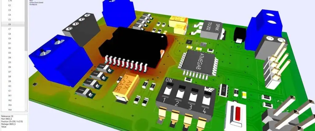
The foundation of your GPS tracker requires several key components working in harmony. The microcontroller serves as the brain of the device, with popular choices including the ESP32 for its built-in WiFi capabilities, Arduino-compatible boards for ease of programming, or specialized IoT development boards that integrate multiple communication protocols.

For GPS functionality, modules like the NEO-8M or NEO-6M from u-blox provide reliable positioning data with good accuracy and reasonable power consumption. These modules communicate via UART and can achieve cold start times under 30 seconds while maintaining hot start capabilities in under one second.

Cellular communication requires a GSM/GPRS module such as the SIM800L, SIM7600, or more advanced LTE modules like the SIM7000 series. These modules handle the data transmission to your backend servers and support various cellular standards depending on your regional requirements and data needs.

Power management is crucial for portable tracking devices. Include a lithium-ion battery with appropriate capacity for your use case, a charging circuit for easy maintenance, and consider solar panels for extended outdoor deployments. Implement sleep modes and efficient power management to maximize battery life between charges.

Additional components include a robust enclosure rated for your intended environment, LED indicators for status feedback, optional buzzers for audio alerts, and mounting hardware appropriate for your tracking application.

Firmware Development and GPS Integration

The firmware development process begins with setting up your development environment and initializing the core systems. Start by configuring the GPS module to receive NMEA sentences, which contain standardized location data including latitude, longitude, altitude, speed, and timestamp information.

Implement a GPS parsing library or create your own parser to extract meaningful data from NMEA sentences. Focus on GGA (Global Positioning System Fix Data) and RMC (Recommended Minimum) sentences, which provide the essential positioning information needed for tracking applications.

Create a location data structure that stores coordinates, timestamps, accuracy measurements, and satellite count. Implement validation logic to ensure GPS fixes are reliable before transmitting data, including checks for minimum satellite count and position accuracy thresholds.

Develop a state machine that manages different operational modes: initialization, GPS acquisition, data transmission, sleep mode, and error handling. This approach ensures reliable operation and efficient power management throughout the device lifecycle.

Cellular Communication Implementation

Establishing cellular communication requires configuring your GSM/GPRS module with the appropriate APN settings for your cellular provider. Implement AT command sequences to initialize the module, establish network connectivity, and manage data transmission sessions.

Design a robust communication protocol that handles network interruptions gracefully. Implement retry mechanisms, data queuing for offline periods, and connection monitoring to ensure reliable data delivery. Consider using MQTT for efficient bidirectional communication, allowing both data transmission and remote configuration capabilities.

Create data packets that include essential tracking information: device ID, timestamp, GPS coordinates, battery level, and any sensor data. Optimize packet size to minimize cellular data usage while maintaining necessary information density.

Implement security measures including data encryption, device authentication, and secure communication protocols. Use TLS/SSL for data transmission and consider implementing device certificates for enhanced security in commercial deployments.

Backend Infrastructure and API Development

The backend infrastructure serves as the central hub for receiving, processing, and storing tracking data from your devices. Design a scalable architecture using cloud services like AWS, Google Cloud Platform, or Azure to handle multiple devices and users efficiently.

Develop RESTful APIs that handle device registration, location data ingestion, user authentication, and data retrieval. Implement endpoints for real-time tracking, historical data queries, geofence management, and device configuration updates.

Choose an appropriate database solution for storing location data. Time-series databases like InfluxDB excel at handling GPS tracking data, while traditional SQL databases can manage user accounts and device relationships. Consider implementing data retention policies to manage storage costs and comply with privacy regulations.

Implement real-time notification systems using WebSockets or Server-Sent Events to provide instant updates to connected mobile applications. This enables live tracking capabilities and immediate alert delivery for geofence violations or emergency situations.

Flutter Mobile Application Development

Flutter provides an excellent framework for creating cross-platform mobile applications that work seamlessly on both iOS and Android devices. Begin by setting up your Flutter development environment and creating a new project with the necessary dependencies for mapping, HTTP communication, and local storage.

Design an intuitive user interface that displays maps, device lists, and tracking information clearly. Implement a main dashboard showing device status, battery levels, and last known positions. Create detailed views for individual devices with historical tracking data and route visualization.

Integrate mapping functionality using packages like Google Maps for Flutter or open-source alternatives like Flutter Map with OpenStreetMap data. Implement features for displaying current device locations, drawing historical routes, and managing geofences with visual boundary indicators.

Develop real-time tracking capabilities by establishing WebSocket connections to your backend services. Implement efficient state management using providers or bloc patterns to handle live location updates and maintain responsive user interfaces.

Create user account management features including registration, authentication, device association, and profile management. Implement secure token-based authentication and consider biometric authentication options for enhanced security.

Advanced Features and Optimization

Enhance your tracking system with advanced features that provide additional value to users. Implement geofencing capabilities that trigger alerts when devices enter or exit predefined areas. Create customizable notification systems that support SMS, email, and push notifications for various tracking events.

Develop offline mapping capabilities for areas with limited internet connectivity. Cache map tiles locally and implement data synchronization when connectivity is restored. This ensures continuous functionality even in remote locations.

Optimize power consumption through intelligent tracking algorithms that adjust GPS sampling rates based on movement patterns. Implement accelerometer-based motion detection to trigger active tracking only when movement is detected, significantly extending battery life during stationary periods.

Create comprehensive analytics dashboards that provide insights into tracking patterns, device usage statistics, and system performance metrics. These analytics help users understand tracking data better and identify optimization opportunities.

Testing and Deployment Strategies

Thorough testing is essential for reliable GPS tracking systems. Conduct extensive field testing in various environments including urban areas with tall buildings, rural locations, and indoor spaces to evaluate GPS performance and cellular connectivity reliability.

Implement automated testing procedures for both firmware and mobile applications. Create unit tests for GPS parsing functions, communication protocols, and API endpoints. Develop integration tests that verify end-to-end functionality from device to mobile application.

Test power consumption extensively under different operational scenarios. Measure battery life during active tracking, sleep modes, and various cellular signal conditions to provide accurate battery life estimates to users.

Consider implementing over-the-air update capabilities for firmware updates and remote configuration changes. This enables bug fixes and feature updates without physical access to deployed devices, significantly reducing maintenance overhead.

Plan your deployment strategy considering regulatory requirements for GPS tracking devices in your target markets. Ensure compliance with privacy laws and consider implementing features that support legal requirements for tracking consent and data management.

Conclusion

Building a comprehensive GPS tracker with cellular communication and Flutter app integration requires careful planning, attention to detail, and thorough testing. The combination of reliable hardware, efficient firmware, robust backend infrastructure, and intuitive mobile applications creates a powerful tracking solution suitable for various applications from personal asset tracking to commercial fleet management.

Success in this project depends on understanding the interconnections between all system components and optimizing each element for reliability, efficiency, and user experience. With proper implementation, your GPS tracking system will provide accurate, real-time location data while maintaining the flexibility and scalability needed for long-term success.

Programming STM32L4 Microcontrollers with Linux, GNU Make, and OpenOCD

The STM32L4 series from STMicroelectronics represents a powerful family of ultra-low-power ARM Cortex-M4 microcontrollers designed for energy-efficient applications. While many developers rely on proprietary IDEs like STM32CubeIDE, developing STM32L4 applications on Linux using open-source tools offers greater flexibility, deeper understanding of the build process, and integration with existing Unix-based workflows. This comprehensive guide explores how to set up and use GNU Make and OpenOCD for STM32L4 development on Linux systems.

YouTube video

Understanding the STM32L4 Architecture

The STM32L4 family features ARM Cortex-M4F cores running at up to 80MHz, with integrated floating-point units and digital signal processing capabilities. These microcontrollers include various memory configurations, typically ranging from 128KB to 2MB of flash memory and 96KB to 640KB of SRAM. The L4 series excels in low-power applications, offering multiple power modes including sleep, stop, and standby modes that can reduce current consumption to mere nanoamps.

Key features include advanced peripherals such as USB OTG, CAN-FD, multiple UART/USART interfaces, SPI, I2C, ADCs with up to 16-bit resolution, and sophisticated timer systems. The microcontrollers support multiple clock sources and feature an internal MSI oscillator that can be dynamically adjusted from 100kHz to 48MHz, making them ideal for battery-powered applications.

Setting Up the Linux Development Environment

Developing for STM32L4 on Linux requires several essential tools. The GNU ARM Embedded Toolchain provides the cross-compiler, linker, and debugging tools necessary for ARM Cortex-M development. Most Linux distributions offer these tools through package managers, though downloading the latest version from ARM’s official releases often provides better optimization and newer features.

bash

# Install essential development tools on Ubuntu/Debian
sudo apt update
sudo apt install gcc-arm-none-eabi gdb-multiarch openocd make git

# Verify installation
arm-none-eabi-gcc --version
openocd --version

The toolchain includes arm-none-eabi-gcc for compilation, arm-none-eabi-ld for linking, arm-none-eabi-objcopy for binary format conversion, and arm-none-eabi-gdb for debugging. These tools understand ARM architecture specifics and generate optimized code for Cortex-M processors.

Additionally, installing STM32CubeMX (available as a Linux package) provides access to STMicroelectronics’ hardware abstraction layer (HAL) libraries, device configuration tools, and reference examples, though it’s not strictly necessary for bare-metal development.

GNU Make for STM32L4 Projects

GNU Make serves as the build system orchestrating the compilation process. A well-structured Makefile for STM32L4 development must handle cross-compilation, linking with appropriate memory layouts, and generating firmware binaries in the correct format.

A typical STM32L4 Makefile begins by defining the target microcontroller and toolchain:

makefile

# Target configuration
TARGET = stm32l476rg
MCU = cortex-m4
FLOAT_ABI = hard
FPU = fpv4-sp-d16

# Toolchain
CC = arm-none-eabi-gcc
LD = arm-none-eabi-ld
OBJCOPY = arm-none-eabi-objcopy
SIZE = arm-none-eabi-size

# Compiler flags
CFLAGS = -mcpu=$(MCU) -mthumb -mfloat-abi=$(FLOAT_ABI) -mfpu=$(FPU)
CFLAGS += -DSTM32L476xx -DUSE_HAL_DRIVER
CFLAGS += -Wall -Wextra -Og -g -ffunction-sections -fdata-sections

The memory layout requires careful attention, as STM32L4 devices have specific memory regions for flash, SRAM, and peripheral addresses. A linker script (typically with a .ld extension) defines these memory regions and section placements:

ld

MEMORY
{
  FLASH (rx) : ORIGIN = 0x08000000, LENGTH = 1024K
  RAM (rwx)  : ORIGIN = 0x20000000, LENGTH = 96K
  RAM2 (rwx) : ORIGIN = 0x10000000, LENGTH = 32K
}

The Makefile should include rules for compiling source files, linking objects, and generating binary outputs:

makefile

# Build rules
%.o: %.c
	$(CC) $(CFLAGS) $(INCLUDES) -c $< -o $@

$(TARGET).elf: $(OBJECTS)
	$(CC) $(CFLAGS) $(LDFLAGS) $^ -o $@

$(TARGET).bin: $(TARGET).elf
	$(OBJCOPY) -O binary $< $@

$(TARGET).hex: $(TARGET).elf
	$(OBJCOPY) -O ihex $< $@

Dependency tracking ensures that changes to header files trigger recompilation of affected source files. Modern Makefiles use automatic dependency generation:

makefile

DEPS = $(OBJECTS:.o=.d)
-include $(DEPS)

%.o: %.c
	$(CC) $(CFLAGS) $(INCLUDES) -MMD -MP -c $< -o $@

OpenOCD Configuration and Usage

OpenOCD (Open On-Chip Debugger) provides the crucial link between development tools and STM32L4 hardware. It supports various debug probes including ST-Link, J-Link, and Black Magic Probe, communicating with the target microcontroller through SWD or JTAG interfaces.

Configuration files tell OpenOCD about the specific hardware setup. For STM32L4 development with an ST-Link programmer, a typical configuration might look like:

tcl

# OpenOCD configuration for STM32L4
source [find interface/stlink.cfg]
source [find target/stm32l4x.cfg]

# Enable semihosting for printf debugging
arm semihosting enable

# Reset configuration
reset_config srst_only

OpenOCD runs as a server, typically listening on port 4444 for telnet connections and port 3333 for GDB connections. Starting OpenOCD with the appropriate configuration enables communication with the target:

bash

# Start OpenOCD with STM32L4 configuration
openocd -f interface/stlink.cfg -f target/stm32l4x.cfg

# In another terminal, connect via telnet
telnet localhost 4444

Common OpenOCD commands include flashing firmware, reading memory, setting breakpoints, and controlling execution:

tcl

# Flash programming
program firmware.elf verify reset

# Memory operations
mdw 0x20000000 16    # Read 16 words from RAM
mww 0x20000000 0x12345678    # Write word to RAM

# Execution control
reset halt
step
resume

Integrating Debugging with GDB

The GNU Debugger (GDB) provides sophisticated debugging capabilities when connected to OpenOCD. The gdb-multiarch package supports multiple architectures including ARM. A typical debugging session begins by connecting GDB to OpenOCD’s GDB server:

bash

# Start debugging session
gdb-multiarch firmware.elf
(gdb) target extended-remote localhost:3333
(gdb) monitor reset halt
(gdb) load
(gdb) break main
(gdb) continue

GDB supports all standard debugging operations: setting breakpoints, examining variables, stepping through code, and analyzing stack traces. For STM32L4 debugging, peripheral registers can be examined directly:

gdb

# Examine GPIO registers
x/4wx 0x48000000    # GPIOA base address
info registers
backtrace
print variable_name

Advanced debugging features include watchpoints for memory locations, conditional breakpoints, and automatic variable display. The Text User Interface (TUI) mode provides a more visual debugging experience:

bash

gdb-multiarch -tui firmware.elf

Project Structure and Best Practices

A well-organized STM32L4 project structure facilitates maintainability and collaboration. A recommended directory layout separates source code, headers, libraries, and build artifacts:

project/
├── src/           # Application source files
├── inc/           # Application headers
├── lib/           # Libraries (HAL, CMSIS)
├── build/         # Compiled objects and binaries
├── scripts/       # Build and utility scripts
├── docs/          # Documentation
├── Makefile       # Build configuration
└── openocd.cfg    # Debug configuration

Version control considerations include ignoring build artifacts while preserving source code and configuration files. A typical .gitignore for STM32L4 projects excludes:

gitignore

build/
*.o
*.elf
*.bin
*.hex
*.map
*.d
.vscode/
*.swp

Code organization should separate hardware abstraction layers from application logic. Using consistent naming conventions, proper header guards, and modular design principles creates maintainable embedded systems.

Advanced Makefile Techniques

Sophisticated STM32L4 Makefiles can automate many development tasks beyond basic compilation. Conditional compilation based on build configurations allows single codebases to target multiple hardware variants:

makefile

# Configuration-specific settings
ifeq ($(CONFIG), DEBUG)
    CFLAGS += -DDEBUG -O0
else ifeq ($(CONFIG), RELEASE)
    CFLAGS += -DNDEBUG -Os
endif

# Multiple target support
ifeq ($(BOARD), NUCLEO_L476RG)
    CFLAGS += -DNUCLEO_L476RG
    LDSCRIPT = stm32l476rg_flash.ld
endif

Automated testing integration can verify builds across multiple configurations:

makefile

.PHONY: test-all
test-all:
	$(MAKE) clean CONFIG=DEBUG
	$(MAKE) all CONFIG=DEBUG
	$(MAKE) clean CONFIG=RELEASE
	$(MAKE) all CONFIG=RELEASE

Optimization and Performance Considerations

STM32L4 development requires careful attention to optimization, particularly for low-power applications. Compiler optimization levels significantly impact both code size and execution speed. The -Os flag optimizes for size, crucial for microcontrollers with limited flash memory, while -O2 optimizes for speed.

Link-time optimization (-flto) can further reduce code size by enabling cross-module optimizations. However, it may complicate debugging, so it’s typically reserved for release builds.

Power consumption optimization involves both software and hardware considerations. Using STM32L4’s low-power modes requires proper clock configuration and peripheral management:

// Example low-power configuration
HAL_PWREx_EnableUltraLowPowerMode();
HAL_PWREx_EnableFastWakeup();
__HAL_RCC_WAKEUPSTOP_CLK_CONFIG(RCC_STOP_WAKEUPCLOCK_MSI);

Troubleshooting Common Issues

STM32L4 development on Linux can present several challenges. Connection issues with debug probes often stem from USB permissions or driver problems. Adding users to the dialout group and installing appropriate udev rules typically resolves these issues:

bash

# Add user to dialout group
sudo usermod -a -G dialout $USER

# Install ST-Link udev rules
sudo cp 49-stlinkv2.rules /etc/udev/rules.d/
sudo udevadm control --reload-rules

Memory-related errors during linking often indicate incorrect linker scripts or memory region definitions. Examining the generated map file helps identify memory usage and potential conflicts.

Build failures frequently result from missing dependencies, incorrect toolchain versions, or path issues. Maintaining consistent development environments across team members prevents many such problems.

Conclusion

Programming STM32L4 microcontrollers on Linux using GNU Make and OpenOCD provides a powerful, flexible development environment that integrates well with modern software development practices. While the initial setup requires more effort than proprietary IDEs, the resulting workflow offers superior automation capabilities, version control integration, and deeper understanding of the embedded development process.

This approach scales well from simple applications to complex, multi-developer projects. The open-source toolchain ensures long-term viability and eliminates vendor lock-in concerns. As embedded systems become increasingly sophisticated, mastering these fundamental tools provides a solid foundation for professional embedded development.

The combination of Linux’s robust development environment, GNU Make’s flexible build system, and OpenOCD’s comprehensive debugging capabilities creates an ideal platform for STM32L4 development that can adapt to changing project requirements and integrate seamlessly with modern DevOps practices.

Wireless LED Control: Building a Bluetooth Arduino LED Control Pad with Processing

In the realm of embedded systems and interactive computing, the ability to control hardware wirelessly opens up countless possibilities for creative projects and practical applications. One of the most accessible and rewarding projects for both beginners and experienced makers is creating a Bluetooth-enabled LED control system using Arduino and Processing. This comprehensive tutorial will guide you through building a sophisticated wireless LED control pad that combines the power of Arduino’s hardware interface with Processing’s intuitive graphical programming environment.

YouTube video

Understanding the Technology Stack

The foundation of this project rests on three key technologies working in harmony. Arduino serves as the hardware controller, managing the LED outputs and handling Bluetooth communication through an HC-05 module. Processing acts as the user interface, providing an elegant control panel that communicates wirelessly with the Arduino. The HC-05 Bluetooth module bridges these two environments, enabling seamless serial communication over a wireless connection.

The beauty of this setup lies in its versatility. While we’ll focus on LED control in this tutorial, the same principles can be extended to control motors, servos, displays, or virtually any hardware component. The Processing interface can be customized to match specific project requirements, making this a valuable foundation for more complex automation systems.

Hardware Requirements and Setup

To build this project, you’ll need several key components. The Arduino Uno serves as the central controller, though other Arduino variants will work equally well. The HC-05 Bluetooth module handles wireless communication, connecting to the Arduino through digital pins 10 and 11 for RX and TX respectively. You’ll also need LEDs with appropriate current-limiting resistors, jumper wires, and a breadboard for prototyping.

The HC-05 module deserves special attention as it’s the heart of the wireless functionality. This versatile Bluetooth module operates on the Serial Port Protocol (SPP), making it compatible with standard serial communication functions. Unlike some Bluetooth modules that can only operate as slaves, the HC-05 can function as both master and slave, opening possibilities for Arduino-to-Arduino communication in future projects.

When wiring the system, the connection setup is straightforward: HC-05 TX connects to Arduino Pin 10, HC-05 RX connects to Arduino Pin 11, VCC connects to 5V, and GND connects to ground. The LEDs connect to digital output pins through current-limiting resistors to prevent damage. A typical 220-ohm to 1k-ohm resistor works well for standard 5mm LEDs.

Arduino Programming Fundamentals

The Arduino code forms the backbone of the hardware control system. The program utilizes the SoftwareSerial library to establish communication with the HC-05 module while preserving the main serial port for debugging and programming. This approach allows you to upload code without disconnecting the Bluetooth module, streamlining the development process.

The Arduino continuously monitors for incoming Bluetooth data, converting received strings into integer action codes that trigger specific LED behaviors. This command parsing system is both simple and expandable. For example, sending “1” might turn on an LED, while “2” turns it off. More complex commands could control LED brightness through PWM or create blinking patterns.

The code structure follows Arduino’s standard setup() and loop() pattern. In setup(), the program initializes serial communication at 9600 baud and configures LED pins as outputs. The loop() function continuously checks for available Bluetooth data, processes commands, and updates LED states accordingly. Error handling ensures the system responds gracefully to unexpected input.

One crucial aspect of the Arduino implementation is the use of SoftwareSerial instead of the hardware serial port. This choice prevents conflicts during code uploads and allows simultaneous Bluetooth communication and serial monitoring for debugging. The 9600 baud rate provides reliable communication while being compatible with most Bluetooth terminal applications.

Processing Interface Development

Processing transforms the user experience by providing an intuitive graphical interface for LED control. Unlike command-line interfaces or mobile apps, Processing allows complete customization of the control panel appearance and functionality. The Processing code imports the serial and ControlP5 libraries to handle Bluetooth communication and create interactive GUI elements.

The ControlP5 library deserves special mention as it provides professional-looking interface elements with minimal coding effort. Buttons, sliders, toggles, and other controls can be easily added and customized. The library handles mouse events, visual feedback, and state management automatically, allowing developers to focus on functionality rather than low-level interface programming.

Serial communication in Processing mirrors Arduino’s approach but from the computer side. The program identifies the correct COM port for the paired HC-05 module and establishes communication at 115200 baud. This higher baud rate compared to typical Arduino projects enables more responsive communication, though the HC-05 module may need reconfiguration to support this speed.

The Processing sketch creates a window containing buttons for various LED control functions. When users click buttons, the program sends corresponding command strings over the Bluetooth connection. The interface can include real-time feedback, showing current LED states or connection status. Advanced implementations might include color pickers for RGB LEDs or sliders for brightness control.

Bluetooth Configuration and Pairing

Successful Bluetooth communication requires proper module configuration and device pairing. The HC-05 module ships with default settings that work for basic applications, but optimizing these settings improves performance and reliability. After pairing the HC-05 with your computer, two COM ports appear in Windows Device Manager under “Ports (COM & LPT)” as “Standard Serial over Bluetooth link”.

The pairing process varies slightly between operating systems but follows similar principles. On Windows, accessing Bluetooth settings and adding a new device initiates the discovery process. The HC-05 typically appears as “HC-05” or a similar identifier. The default pairing PIN is usually “1234” or “0000,” depending on the specific module variant.

Understanding the dual COM port nature of Bluetooth communication is crucial for troubleshooting connection issues. One port handles incoming data while the other manages outgoing data. Processing must connect to the outgoing COM port, usually marked as “dev” in the device manager, to successfully send commands to the Arduino.

For projects requiring custom module settings, AT command mode provides access to advanced configuration options. This mode allows changing the device name, baud rate, PIN code, and other parameters. However, most projects work perfectly with default settings, making AT commands optional for basic implementations.

Advanced Features and Customization

The basic LED control system serves as a foundation for numerous enhancements and customizations. RGB LED support transforms simple on/off control into full-color lighting systems. By implementing PWM control on Arduino and color picker interfaces in Processing, users can select any color from the spectrum and see immediate results.

Pattern generation adds another dimension to LED control. Arduino can store and execute complex blinking patterns, light chases, or synchronized displays across multiple LEDs. Processing interfaces can include pattern editors, allowing users to create custom sequences and upload them wirelessly to the Arduino for execution.

Multi-Arduino support extends the system’s capabilities dramatically. Since the HC-05 can operate in master mode, one Arduino can coordinate multiple slave units, creating distributed lighting systems or synchronized device networks. This approach enables large-scale installations while maintaining centralized control through Processing.

Real-time monitoring capabilities transform the one-way control system into a two-way communication channel. Arduino can send sensor readings, system status, or diagnostic information back to Processing for display. This feedback mechanism enables responsive interfaces that adapt to changing conditions or provide system health monitoring.

Troubleshooting and Optimization

Common issues in Bluetooth Arduino projects typically involve communication failures, pairing problems, or code upload difficulties. Connection issues often stem from incorrect COM port selection in Processing or Arduino code upload conflicts when Bluetooth modules remain connected. A standard troubleshooting step involves disconnecting TX and RX pins during code uploads, then reconnecting them afterward.

Baud rate mismatches between Arduino and Processing cause garbled communication or complete communication failure. Ensuring both sides use identical baud rates resolves most data transmission issues. Some HC-05 modules require AT commands to change from the default 9600 baud to higher speeds.

Range and interference problems affect wireless performance in environments with multiple Bluetooth devices or Wi-Fi networks. The HC-05’s typical 10-meter range works well for most applications, but obstacles and interference can reduce effective range. Positioning the module away from metal objects and other electronic devices often improves performance.

Power supply issues manifest as erratic behavior or communication dropouts. The HC-05 module requires stable 3.3V to 5V power with adequate current capacity. When powering multiple LEDs or other components, ensure the Arduino’s built-in regulator can handle the total current draw, or consider external power supplies for high-current applications.

Future Possibilities and Project Extensions

The Bluetooth Arduino LED control system opens doors to countless exciting possibilities. Home automation represents one of the most practical extensions, where the LED control principles apply to lighting systems, appliances, or security devices. The Processing interface can expand to include scheduling, remote monitoring, and integration with other smart home platforms.

Educational applications benefit from the visual and interactive nature of LED control systems. Students can learn programming concepts, electronics principles, and wireless communication through hands-on experimentation. The immediate visual feedback makes abstract concepts tangible and engaging.

Professional applications might include stage lighting control, architectural installations, or prototype development for IoT devices. The combination of Arduino’s reliability, Processing’s interface capabilities, and Bluetooth’s ubiquity creates a powerful platform for both permanent installations and temporary displays.

Conclusion

Building a Bluetooth Arduino LED control pad with Processing demonstrates the power of combining different technologies to create intuitive, wireless control systems. This project teaches fundamental concepts in embedded programming, wireless communication, and user interface design while producing a practical tool with numerous applications.

The skills developed through this project transfer directly to more complex endeavors in home automation, robotics, and IoT development. As you experiment with different LED patterns, interface designs, and system expansions, you’ll develop the expertise needed to tackle increasingly sophisticated wireless control challenges.

Whether you’re a student learning the basics of electronics and programming or an experienced developer exploring new interface possibilities, this Bluetooth LED control system provides a solid foundation for understanding wireless hardware communication and interactive system design.

How to Connect Raspberry Pi to CAN Bus

The Controller Area Network (CAN) bus is a robust vehicle bus standard designed to allow microcontrollers and devices to communicate with each other’s applications without a host computer. Originally developed by Bosch for automotive applications, CAN bus has expanded into industrial automation, medical equipment, and IoT projects. Connecting a Raspberry Pi to a CAN bus opens up exciting possibilities for automotive diagnostics, industrial monitoring, and embedded system development.

YouTube video

Understanding CAN Bus Fundamentals

CAN bus operates on a differential signaling system using two wires: CAN High (CANH) and CAN Low (CANL). The protocol uses a twisted pair cable that provides excellent noise immunity and allows for reliable communication over distances up to 1 kilometer at lower speeds or shorter distances at higher speeds. The bus operates at various speeds, commonly 125 kbps, 250 kbps, 500 kbps, and 1 Mbps.

The protocol follows a multi-master architecture where any node can initiate communication, and message priority is determined by the identifier field. CAN frames contain an identifier, control field, data field (0-8 bytes), CRC field, and acknowledgment field. The bus uses non-destructive arbitration, meaning higher priority messages automatically take precedence without data loss.

Required Hardware Components

To connect a Raspberry Pi to CAN bus, you’ll need several key components. The most critical is a CAN transceiver module, which converts the digital signals from the Raspberry Pi into the differential CAN bus signals. Popular options include the MCP2515 with TJA1050 transceiver, which connects via SPI, or more advanced solutions like the Waveshare RS485/CAN HAT.

You’ll also need appropriate cabling – typically 120-ohm twisted pair cable for automotive applications, though standard Cat5 cable can work for prototyping. Termination resistors (120 ohms) are essential at both ends of the bus to prevent signal reflections. A breadboard or PCB for connections, jumper wires, and potentially level shifters if interfacing with 12V automotive systems complete the hardware requirements.

Software Setup and Configuration

Begin by enabling SPI on your Raspberry Pi using sudo raspi-config and selecting “Interfacing Options” then “SPI.” Update your system with sudo apt update && sudo apt upgrade to ensure you have the latest packages.

Install the necessary CAN utilities with sudo apt install can-utils. These tools provide command-line interfaces for CAN network configuration and debugging. The kernel modules for CAN support are typically included in modern Raspberry Pi OS distributions, but you may need to load them manually using sudo modprobe can and sudo modprobe can-raw.

For MCP2515-based modules, add the following lines to /boot/config.txt:

dtparam=spi=on
dtoverlay=mcp2515-can0,oscillator=8000000,interrupt=25
dtoverlay=spi-bcm2835-overlay

The oscillator frequency should match your module’s crystal frequency, commonly 8MHz or 16MHz. The interrupt pin typically connects to GPIO25 but verify this matches your wiring.

Physical Connections and Wiring

Proper wiring is crucial for reliable CAN bus operation. For MCP2515 modules, connect VCC to 3.3V or 5V depending on your module, GND to ground, CS to SPI CE0 (GPIO8), SI to SPI MOSI (GPIO10), SO to SPI MISO (GPIO9), and SCK to SPI SCLK (GPIO11). The interrupt pin typically connects to GPIO25.

The CAN connections involve CANH and CANL wires forming the differential pair. These connect to your CAN network, which must be properly terminated with 120-ohm resistors at each end. In automotive applications, you’ll typically find these connections at the OBD-II port, where pins 6 and 14 correspond to CANH and CANL respectively.

Pay careful attention to power supply requirements. Automotive environments operate at 12V, while Raspberry Pi uses 3.3V logic. Ensure your CAN transceiver module handles this voltage translation, or use appropriate level shifters and voltage regulators.

Network Configuration

Once hardware is connected, configure the CAN network interface. First, set the bitrate matching your CAN network. Common automotive networks use 500kbps for high-speed CAN or 125kbps for low-speed networks. Use the command:

bash

sudo ip link set can0 up type can bitrate 500000

Verify the interface is active with ip link show can0. You should see the interface in the UP state. For automatic configuration on boot, add these commands to /etc/rc.local or create a systemd service.

Configure error handling and restart policies using sudo ip link set can0 type can restart-ms 100 to automatically restart the interface after bus-off conditions. This is particularly important in automotive environments where temporary faults are common.

Testing and Verification

Test your connection using the included CAN utilities. Use candump can0 to monitor all traffic on the bus, which will display incoming messages in real-time. To send test messages, use cansend can0 123#DEADBEEF where 123 is the CAN ID and DEADBEEF is the data payload in hexadecimal.

For more advanced testing, cangen can0 generates random CAN traffic for load testing, while canstat can0 provides statistics about bus utilization and error rates. These tools help verify that your connection is working correctly and the bus is operating within normal parameters.

Programming with Python

Python provides excellent libraries for CAN bus communication. Install the python-can library using pip3 install python-can. This library supports multiple CAN interfaces and provides a consistent API for CAN communication.

A basic example for receiving messages:

python

import can

bus = can.interface.Bus(channel='can0', bustype='socketcan')

while True:
    message = bus.recv()
    print(f"ID: {message.arbitration_id:x}, Data: {message.data.hex()}")

For sending messages:

python

import can

bus = can.interface.Bus(channel='can0', bustype='socketcan')
message = can.Message(arbitration_id=0x123, data=[0xDE, 0xAD, 0xBE, 0xEF])
bus.send(message)

Troubleshooting Common Issues

Several issues commonly arise when connecting Raspberry Pi to CAN bus. If the interface fails to come up, verify SPI is enabled and the correct device tree overlay is loaded. Check physical connections, ensuring proper power supply and that the CAN transceiver has appropriate voltage levels.

Bus timing issues often manifest as high error rates or inability to communicate. Verify the bitrate matches the network, and ensure proper termination resistors are installed. Oscilloscope measurement of CANH and CANL signals can reveal timing or electrical issues.

If messages aren’t received, check that the bus isn’t in error-passive or bus-off state using ip -details link show can0. Reset the interface with sudo ip link set can0 down followed by sudo ip link set can0 up type can bitrate 500000.

Advanced Applications and Use Cases

Once basic connectivity is established, numerous advanced applications become possible. Automotive diagnostics using OBD-II protocols allow reading engine parameters, fault codes, and emissions data. Industrial automation applications can monitor PLCs, sensors, and actuators on factory floors.

Building CAN gateways enables protocol translation between CAN and Ethernet, WiFi, or cellular networks, enabling remote monitoring and control. Data logging applications can capture and analyze CAN traffic for system optimization or fault analysis.

Security Considerations

CAN bus networks lack built-in security features, making proper security implementation crucial. Implement message filtering to process only expected message IDs and validate message content before acting on received data. Consider implementing encryption or authentication layers for sensitive applications.

Network segmentation using CAN bridges or gateways can isolate critical systems from less secure networks. Regular security audits and monitoring for unusual traffic patterns help detect potential intrusions or system compromises.

Conclusion

Connecting Raspberry Pi to CAN bus opens doors to automotive diagnostics, industrial automation, and IoT applications. Success requires understanding CAN fundamentals, proper hardware selection, correct wiring practices, and appropriate software configuration. With careful attention to these details, you can build robust systems that reliably communicate on CAN networks, whether for hobbyist projects, professional development, or commercial applications. The combination of Raspberry Pi’s computing power and CAN bus’s reliability creates a powerful platform for embedded system development.

From Smartphones to Robotics: How 3D-MID Is Powering Next-Gen Devices

The electronics industry is experiencing a revolutionary transformation, driven by the demand for smaller, more efficient, and increasingly complex devices. At the heart of this evolution lies 3D-MID (Molded Interconnect Device) technology, also known as 3D Circuits, which is reshaping how we design and manufacture everything from smartphones to advanced robotics systems. This innovative approach to circuit integration is not just changing the game—it’s redefining the entire playing field.

YouTube video

Understanding 3D-MID Technology: The Foundation of Modern Electronics

3D-MID technology represents a paradigm shift from traditional flat circuit boards to three-dimensional electronic structures. Unlike conventional PCBs (Printed Circuit Boards) that are typically flat and require separate mechanical housings, 3D-MID combines the circuit carrier and mechanical structure into a single, integrated component. This revolutionary approach creates 3D circuits that can be molded into virtually any shape, enabling unprecedented design flexibility and functionality.

The technology works by creating a plastic substrate using injection molding, followed by selective metallization to create conductive pathways. These pathways form the electrical connections necessary for component mounting and signal transmission. The result is a single component that serves both as the mechanical structure and the electrical circuit, eliminating the need for separate housing and interconnection components.

The 3D-MID Manufacturing Process: Precision Meets Innovation

The creation of 3D circuits involves several sophisticated manufacturing steps that showcase the technology’s precision and versatility. The process begins with injection molding using thermoplastic materials that have been specially formulated for electronic applications. These materials must possess excellent electrical properties, dimensional stability, and the ability to withstand the subsequent metallization processes.

During the molding phase, specific areas of the plastic substrate are designed to become conductive pathways. This is achieved through various techniques, including laser direct structuring (LDS), two-shot molding, or masking and etching processes. The LDS method, in particular, has gained significant traction due to its precision and efficiency. It involves adding a metal-plastic additive to the base material, which is then activated by laser treatment to create selective metallization areas.

Following the structural formation, the metallization process creates the actual 3D circuits. This typically involves electroless plating, where copper and other metals are deposited onto the activated areas. The result is a robust, reliable electrical pathway that can handle the demanding requirements of modern electronic devices.

Revolutionizing Smartphone Design with 3D-MID

The smartphone industry has been one of the earliest and most enthusiastic adopters of 3D-MID technology. As consumers demand thinner, lighter, and more feature-rich devices, traditional manufacturing approaches have reached their limits. 3D circuits provide the solution by enabling radical miniaturization while maintaining or even improving functionality.

In modern smartphones, 3D-MID components serve multiple critical functions. Antenna systems represent one of the most significant applications, where the technology enables the integration of multiple antennas—including Wi-Fi, Bluetooth, cellular, and NFC—into compact, three-dimensional structures. These 3D circuits can be shaped to fit perfectly within the available space while optimizing signal performance and reducing interference between different communication systems.

Camera modules in smartphones also benefit tremendously from 3D-MID technology. The complex mechanical and electrical requirements of modern camera systems, including autofocus mechanisms, image stabilization, and multiple lens configurations, can be integrated into single 3D circuit components. This integration not only saves space but also improves reliability by reducing the number of interconnections and potential failure points.

Furthermore, sensor integration has been revolutionized by 3D-MID technology. Accelerometers, gyroscopes, magnetometers, and other sensors can be mounted directly onto 3D circuits that are specifically shaped to optimize their performance and position within the device. This level of integration was simply impossible with traditional flat PCB designs.

Robotics: Where 3D-MID Technology Truly Shines

The robotics industry represents perhaps the most exciting frontier for 3D-MID applications. Robots require complex electronic systems that must fit within articulated joints, curved surfaces, and confined spaces—requirements that are perfectly suited to 3D circuits technology.

In robotic arms and manipulators, 3D-MID components enable the integration of sensors, actuators, and control electronics directly into the mechanical structure. This integration eliminates bulky cable harnesses and separate control boxes, resulting in more agile, responsive, and reliable robotic systems. The ability to create 3D circuits that conform to the exact shape of robotic joints and linkages opens up entirely new possibilities for robot design.

Humanoid robots particularly benefit from 3D-MID technology. The complex curves and contours of human-like forms can be perfectly matched with 3D circuits that provide the necessary electronic functionality while maintaining the desired aesthetic and ergonomic properties. Sensors for touch, pressure, temperature, and position can be seamlessly integrated into the robot’s “skin,” creating more natural and intuitive human-robot interactions.

Autonomous vehicles and drones represent another significant application area for 3D circuits. These systems require numerous sensors, communication devices, and control electronics that must be integrated into aerodynamic and space-constrained designs. 3D-MID technology enables the creation of conformal electronic systems that can be embedded directly into vehicle bodies and wing structures.

Advantages of 3D-MID Over Traditional Electronics Manufacturing

The transition to 3D-MID technology offers numerous compelling advantages over traditional electronics manufacturing approaches. Space efficiency stands as perhaps the most significant benefit, with 3D circuits typically requiring 60-80% less volume than equivalent flat PCB implementations. This dramatic space savings enables entirely new product categories and form factors that were previously impossible.

Weight reduction is another crucial advantage, particularly important in aerospace, automotive, and mobile applications. By eliminating separate mechanical housings and reducing the need for interconnection hardware, 3D-MID components can achieve weight savings of 40-70% compared to traditional designs.

Reliability improvements are equally impressive. 3D circuits reduce the number of solder joints, connectors, and cable assemblies—all potential failure points in electronic systems. The integrated nature of 3D-MID technology creates more robust systems that can better withstand vibration, thermal cycling, and mechanical stress.

Cost considerations also favor 3D-MID technology, particularly in high-volume applications. While the initial tooling costs may be higher, the elimination of assembly steps, reduced material usage, and improved yields often result in lower overall manufacturing costs. Additionally, the reduced testing and quality control requirements for integrated 3D circuits contribute to further cost savings.

Emerging Applications and Future Possibilities

The potential applications for 3D-MID technology continue to expand as engineers and designers recognize the possibilities offered by 3D circuits. The medical device industry is embracing this technology for implantable devices, wearable health monitors, and surgical instruments where space constraints and biocompatibility are critical factors.

Automotive applications are rapidly growing, with 3D circuits being integrated into everything from advanced driver assistance systems to electric vehicle charging infrastructure. The ability to create conformal electronic systems that can be embedded directly into vehicle structures opens up new possibilities for sensor integration and system optimization.

The Internet of Things (IoT) represents another significant growth area for 3D-MID technology. The requirements for small, efficient, and cost-effective connected devices align perfectly with the capabilities of 3D circuits. Smart home devices, industrial sensors, and environmental monitoring systems all benefit from the integration possibilities offered by this technology.

Challenges and Considerations in 3D-MID Implementation

Despite its numerous advantages, 3D-MID technology does present certain challenges that must be carefully considered during implementation. Design complexity is significantly higher than traditional PCB design, requiring specialized software tools and expertise in three-dimensional circuit layout. Engineers must consider not only electrical performance but also mechanical stress, thermal management, and manufacturing constraints in three dimensions.

Material selection becomes more critical with 3D circuits, as the plastic substrate must provide both mechanical strength and electrical performance. The thermal expansion characteristics, chemical compatibility, and long-term stability of the materials directly impact the reliability and performance of the final product.

Manufacturing tolerances are also more challenging to achieve with 3D-MID technology. The three-dimensional nature of the components requires precise control over multiple geometric parameters, and the metallization process must provide consistent electrical properties across complex surfaces.

The Future of 3D-MID Technology

Looking ahead, 3D-MID technology is poised for continued growth and innovation. Advances in materials science are enabling higher performance substrates with improved electrical and mechanical properties. New metallization techniques are providing better adhesion, conductivity, and reliability for 3D circuits.

The integration of active components directly into 3D-MID structures represents an exciting frontier. Research into conductive polymers, printed electronics, and embedded semiconductors could enable 3D circuits that incorporate not just passive interconnections but active electronic functions as well.

Machine learning and artificial intelligence are also being applied to 3D-MID design optimization, enabling automated design tools that can optimize both electrical and mechanical performance simultaneously. These advances will make 3D circuits more accessible to a broader range of engineers and applications.

Conclusion: The 3D-MID Revolution

3D-MID technology represents more than just an incremental improvement in electronics manufacturing—it’s a fundamental shift that enables entirely new approaches to product design and functionality. From the smartphones in our pockets to the robots that will shape our future, 3D circuits are becoming the backbone of next-generation devices.

As the technology continues to mature and costs decrease, we can expect to see 3D-MID applications proliferate across virtually every industry that relies on electronic systems. The ability to create truly three-dimensional electronic structures that integrate mechanical and electrical functions will continue to drive innovation and enable products that were previously impossible to imagine.

The future belongs to 3D circuits, and that future is arriving faster than ever before. Organizations that embrace 3D-MID technology today will be best positioned to lead tomorrow’s technological revolution.

Xilinx FPGA end-to-end Ethereum Mining Acceleration System

Xilinx Artix 7

Introduction

Field Programmable Gate Arrays (FPGAs) represent a unique class of reconfigurable hardware that bridges the gap between software flexibility and hardware performance. Xilinx, now part of AMD, has been a leading provider of FPGA technology, offering solutions that have found applications across numerous domains, including cryptocurrency mining. While Ethereum transitioned from Proof of Work to Proof of Stake in September 2022, the technological principles and implementations of FPGA-based mining acceleration systems remain highly relevant for educational purposes and other cryptocurrency mining applications.

This comprehensive analysis explores the design, implementation, and optimization of Xilinx FPGA-based Ethereum mining acceleration systems, examining the technical challenges, architectural considerations, and performance characteristics that defined this innovative approach to cryptocurrency mining.

YouTube video

Background: Ethereum Mining and the Ethash Algorithm

Ethereum mining, before the transition to Proof of Stake, relied on the Ethash algorithm, a memory-hard proof-of-work function designed to be ASIC-resistant. Unlike Bitcoin’s SHA-256 algorithm, Ethash was specifically engineered to level the playing field between different types of mining hardware by requiring substantial memory bandwidth and capacity.

The Ethash algorithm operates through several key stages:

  1. DAG Generation: Creates a large directed acyclic graph (DAG) that grows over time, reaching sizes of several gigabytes
  2. Hash Computation: Performs pseudorandom memory accesses to the DAG while computing hashes
  3. Nonce Search: Iteratively searches for nonce values that produce hash results meeting the network difficulty target

This memory-intensive nature made Ethash particularly suitable for GPU mining, as graphics cards possessed the necessary memory bandwidth and parallel processing capabilities. However, it also presented unique opportunities for FPGA implementation, leveraging the reconfigurable nature of these devices to create highly optimized mining accelerators.

Xilinx FPGA Architecture and Advantages

Xilinx FPGAs offer several architectural advantages that make them compelling platforms for cryptocurrency mining acceleration:

Reconfigurable Logic Fabric

The fundamental strength of Xilinx FPGAs lies in their reconfigurable logic fabric, consisting of configurable logic blocks (CLBs), digital signal processing (DSP) slices, and block RAM (BRAM) resources. This architecture allows for the implementation of custom datapaths optimized specifically for the computational requirements of mining algorithms.

High-Bandwidth Memory Interfaces

Modern Xilinx FPGAs, particularly those in the Ultrascale+ family, support high-bandwidth memory (HBM) and DDR4 interfaces capable of delivering the memory bandwidth required for efficient Ethash computation. The ability to implement custom memory controllers enables optimization of memory access patterns for maximum throughput.

Parallel Processing Capabilities

The inherently parallel nature of FPGA architecture allows for the implementation of multiple independent mining cores on a single device. This parallelism can be exploited at multiple levels, from individual hash function implementations to complete mining pipeline parallelization.

Power Efficiency

When properly optimized, FPGA implementations can achieve superior power efficiency compared to GPU-based mining solutions, particularly important given the energy-intensive nature of cryptocurrency mining operations.

System Architecture Design

xilinx-spartan-6-fpga-tutorial

High-Level System Overview

A comprehensive Xilinx FPGA-based Ethereum mining acceleration system consists of several interconnected components:

Host Interface Layer: Manages communication between the FPGA and host system, typically implemented through PCIe interfaces. This layer handles work distribution, result collection, and system configuration.

Work Distribution Engine: Coordinates the distribution of mining work packages across multiple parallel mining cores, ensuring optimal utilization of available computational resources.

Mining Core Array: The heart of the acceleration system, consisting of multiple parallel Ethash computation engines, each capable of independent operation.

Memory Subsystem: Implements high-performance memory controllers and manages the storage and access of the large DAG dataset required for Ethash computation.

Result Processing Pipeline: Handles the verification and formatting of mining results before transmission back to the host system.

Memory Subsystem Design

The memory subsystem represents one of the most critical components of an FPGA-based Ethash mining system. The DAG dataset, which can exceed 4GB in size, must be stored in external memory and accessed with high bandwidth to maintain computational throughput.

Effective memory subsystem design typically employs:

Multi-Port Memory Controllers: Implementation of multiple independent memory controllers to maximize aggregate bandwidth and reduce access conflicts between parallel mining cores.

Intelligent Caching Strategies: Given the pseudorandom nature of DAG accesses in Ethash, sophisticated caching mechanisms can significantly improve effective memory bandwidth utilization.

Memory Access Optimization: Custom memory access scheduling algorithms that account for the specific access patterns of the Ethash algorithm to minimize latency and maximize throughput.

Mining Core Implementation

Each mining core represents a self-contained Ethash computation engine optimized for FPGA implementation. The core design typically includes:

Keccak-256 Hash Units: Highly optimized implementations of the SHA-3 Keccak hash function, often utilizing dedicated DSP resources for maximum performance.

DAG Access Logic: Specialized circuitry for managing the complex memory access patterns required by the Ethash algorithm.

Nonce Management: Efficient nonce generation and tracking mechanisms to ensure comprehensive search space coverage.

Result Validation: On-chip verification of mining results to reduce unnecessary data transfers to the host system.

Performance Optimization Strategies

Pipeline Optimization

Effective FPGA mining implementations rely heavily on deep pipeline architectures to maximize throughput. Key optimization strategies include:

Computational Pipeline Balancing: Careful analysis and balancing of pipeline stages to eliminate bottlenecks and ensure maximum clock frequency operation.

Memory Access Pipelining: Implementation of sophisticated memory access pipelines that can sustain multiple concurrent DAG lookups while maintaining data coherency.

Result Processing Overlap: Overlapping result processing operations with ongoing computation to minimize idle time and maximize effective utilization.

Resource Utilization Optimization

Xilinx FPGAs offer diverse computational resources that must be carefully allocated for optimal performance:

DSP Slice Utilization: Strategic use of dedicated DSP slices for performance-critical arithmetic operations within the hash computation pipeline.

BRAM Resource Management: Efficient utilization of on-chip block RAM resources for high-frequency data storage and intermediate result buffering.

Logic Resource Optimization: Careful design to maximize the number of parallel mining cores that can be implemented within the available logic resources.

Clock Domain Management

Complex FPGA mining systems often require multiple clock domains to optimize different subsystem operations:

Memory Interface Clocking: Optimization of memory controller clock frequencies to match external memory device specifications and maximize bandwidth.

Computational Core Clocking: Independent optimization of mining core clock frequencies based on critical path analysis and thermal constraints.

Interface Clock Management: Proper management of interface clocks for PCIe and other communication protocols to ensure reliable operation.

Challenges and Implementation Considerations

Thermal Management

FPGA-based mining systems generate significant heat, particularly when operating at maximum performance levels. Effective thermal management strategies include:

Dynamic Voltage and Frequency Scaling: Implementation of adaptive power management techniques that adjust operating parameters based on thermal feedback.

Workload Balancing: Intelligent distribution of computational workload to prevent thermal hotspots and ensure uniform heat distribution across the device.

Cooling System Integration: Design considerations for integration with advanced cooling solutions, including liquid cooling systems for high-performance implementations.

Development Complexity

FPGA-based mining system development presents significant technical challenges:

Algorithm Implementation Complexity: The complexity of implementing optimized Ethash computation engines in hardware description languages requires specialized expertise.

Verification and Validation: Comprehensive testing and validation of complex parallel systems to ensure correctness and reliability under all operating conditions.

Tool Chain Optimization: Effective utilization of Xilinx development tools and optimization flows to achieve optimal implementation results.

Economic Considerations

The viability of FPGA-based mining systems depends on several economic factors:

Development Costs: Significant upfront investment in development time and expertise required to create competitive implementations.

Hardware Costs: FPGA devices, particularly high-end models suitable for mining applications, represent substantial capital investments.

Performance Scalability: The ability to scale performance through parallel device deployment while maintaining economic viability.

Future Implications and Technological Legacy

While Ethereum’s transition to Proof of Stake ended the era of traditional mining on this network, the technological innovations developed for FPGA-based mining systems continue to have broader implications:

Alternative Cryptocurrency Mining

Many other cryptocurrencies continue to utilize proof-of-work consensus mechanisms, creating ongoing opportunities for FPGA-based mining acceleration. The flexible nature of FPGA implementations allows for adaptation to different algorithms with relatively modest development effort.

Computational Acceleration Applications

The optimization techniques and architectural innovations developed for mining applications have found broader applications in high-performance computing, financial modeling, and machine learning acceleration.

Educational and Research Value

FPGA-based mining systems serve as excellent educational platforms for understanding hardware acceleration, parallel computing architectures, and the intersection of computer architecture with economic incentive systems.

Conclusion

Xilinx FPGA-based Ethereum mining acceleration systems represented a sophisticated intersection of reconfigurable computing technology and cryptocurrency economics. These systems demonstrated the potential for FPGA technology to deliver high-performance, power-efficient solutions for computationally intensive applications while highlighting the complex design challenges inherent in developing such systems.

The technical innovations developed during this period continue to influence modern approaches to hardware acceleration and demonstrate the ongoing relevance of FPGA technology in addressing emerging computational challenges. As the cryptocurrency landscape continues to evolve, the fundamental principles and optimization strategies developed for these systems remain valuable for understanding the broader potential of reconfigurable computing in high-performance applications.

The legacy of FPGA-based mining systems extends beyond their original application, contributing to the broader understanding of hardware acceleration, parallel processing architectures, and the economic factors that drive technological innovation in emerging computing domains.

How to Type on LCD Using Bluetooth: Complete Guide

Introduction

In today’s interconnected world, the ability to input text efficiently on devices with LCD displays has become increasingly important. Whether you’re working with a tablet, smartphone, smart TV, or other LCD-equipped device, Bluetooth connectivity offers a wireless solution for text input that can dramatically improve your productivity and user experience. This comprehensive guide will walk you through everything you need to know about typing on LCD displays using Bluetooth technology.

YouTube video

Understanding the Technology

What is Bluetooth?

Bluetooth is a short-range wireless communication technology that allows devices to connect and exchange data without cables. Operating in the 2.4 GHz frequency band, Bluetooth creates a personal area network (PAN) that typically extends up to 30 feet. For typing applications, Bluetooth provides a reliable, low-latency connection between input devices like keyboards and output devices with LCD displays.

LCD Display Integration

LCD (Liquid Crystal Display) technology is found in countless devices today, from smartphones and tablets to laptops, smart TVs, and even refrigerators. When these devices support Bluetooth connectivity, they can receive input from external keyboards, mice, and other peripherals, transforming how we interact with these displays.

Device Compatibility and Setup

Smartphones and Tablets

Most modern smartphones and tablets support Bluetooth keyboard connectivity, making them excellent candidates for enhanced text input.

Android Devices:

  1. Navigate to Settings > Bluetooth
  2. Ensure Bluetooth is enabled
  3. Put your Bluetooth keyboard in pairing mode
  4. Select “Pair new device” or “Add device”
  5. Choose your keyboard from the list of available devices
  6. Enter any required pairing code if prompted

iOS Devices:

  1. Open Settings > Bluetooth
  2. Toggle Bluetooth on if it’s not already active
  3. Set your keyboard to discoverable mode
  4. Tap your keyboard name when it appears in “Other Devices”
  5. Complete any additional pairing steps as prompted

Smart TVs and Streaming Devices

Many smart TVs and streaming devices now support Bluetooth keyboards, making it easier to search for content, enter passwords, and navigate interfaces.

General Setup Process:

  1. Access your TV’s settings menu using the remote
  2. Navigate to Network or Bluetooth settings
  3. Enable Bluetooth if it’s not already active
  4. Put your keyboard in pairing mode
  5. Select “Add Device” or “Search for Devices”
  6. Choose your keyboard and complete the pairing process

Laptops and Computers

While laptops typically have built-in keyboards, Bluetooth connectivity allows for external keyboard use, which can be particularly useful for ergonomic setups or when using the laptop as a desktop replacement.

Windows Setup:

  1. Click the Start button and select Settings
  2. Choose Devices > Bluetooth & other devices
  3. Click “Add Bluetooth or other device”
  4. Select Bluetooth and choose your keyboard
  5. Follow the on-screen instructions to complete pairing

macOS Setup:

  1. Open System Preferences > Bluetooth
  2. Ensure Bluetooth is turned on
  3. Put your keyboard in discoverable mode
  4. Click “Connect” when your keyboard appears
  5. Enter any required pairing code

Types of Bluetooth Input Devices

Physical Keyboards

Physical Bluetooth keyboards offer the most familiar typing experience and come in various form factors:

Full-Size Keyboards: Provide all standard keys including number pad, function keys, and arrow keys. Ideal for productivity work and extended typing sessions.

Compact Keyboards: Smaller footprint while maintaining most functionality. Perfect for travel and limited desk space.

Foldable Keyboards: Ultra-portable options that fold for easy transport. Great for mobile professionals and frequent travelers.

Gaming Keyboards: Feature backlit keys, programmable functions, and enhanced durability for gaming applications.

Virtual and Alternative Input Methods

On-Screen Keyboards: Many devices display virtual keyboards on their LCD screens when text input is required. While not technically Bluetooth-based, these often work in conjunction with Bluetooth mice for point-and-click typing.

Voice Input: Some devices support Bluetooth headsets for voice-to-text input, providing hands-free typing alternatives.

Stylus Input: Bluetooth-enabled styluses can provide handwriting recognition and text input on compatible LCD displays.

Optimizing Your Typing Experience

Keyboard Settings and Customization

Once connected, most operating systems allow you to customize your Bluetooth keyboard experience:

Key Mapping: Assign specific functions to function keys or create custom shortcuts for frequently used commands.

Input Languages: Configure multiple keyboard languages for multilingual typing support.

Auto-Correction: Enable or disable autocorrect features based on your preferences and use case.

Key Repeat Rates: Adjust how quickly keys repeat when held down to match your typing style.

Battery Management

Bluetooth keyboards require power management to ensure consistent performance:

Battery Monitoring: Regularly check battery levels and keep spare batteries or charging cables available.

Power Saving Features: Utilize sleep modes and auto-shutoff features to extend battery life.

Charging Habits: For rechargeable keyboards, maintain good charging practices to preserve battery longevity.

Troubleshooting Common Issues

Connection Problems

Intermittent Disconnections:

  • Check battery levels in your keyboard
  • Ensure devices are within optimal range (typically 30 feet or less)
  • Remove interference from other wireless devices
  • Clear Bluetooth cache on your device if available

Pairing Failures:

  • Reset your keyboard by turning it off and on
  • Clear previous pairing data from both devices
  • Ensure keyboard is in discoverable mode during pairing
  • Try pairing with devices closer together

Input Lag or Delay:

  • Check for interference from other 2.4 GHz devices
  • Ensure both devices have adequate battery power
  • Close unnecessary background applications that might be consuming system resources
  • Consider updating device drivers or firmware

Performance Issues

Missed Keystrokes:

  • Clean keyboard contacts and check for physical damage
  • Verify keyboard is properly paired and connected
  • Check for driver updates for your specific keyboard model
  • Test keyboard with different devices to isolate the issue

Incorrect Character Input:

  • Verify keyboard language settings match your region
  • Check for stuck modifier keys (Shift, Ctrl, Alt)
  • Ensure keyboard layout is correctly configured in device settings
  • Reset keyboard to factory defaults if problems persist

Advanced Features and Applications

Multi-Device Connectivity

Many modern Bluetooth keyboards support connection to multiple devices simultaneously:

Device Switching: Use dedicated keys or key combinations to switch between connected devices quickly.

Profile Management: Maintain separate settings and preferences for different connected devices.

Seamless Workflow: Work across multiple devices without reconnecting or reconfiguring your keyboard.

Specialized Applications

Presentation Control: Use Bluetooth keyboards to control presentations on LCD displays during meetings or conferences.

Media Center Control: Navigate streaming services and media libraries using keyboard shortcuts and navigation keys.

Gaming Integration: Utilize gaming keyboards with LCD-equipped gaming systems for enhanced control and customization.

Home Automation: Control smart home devices with LCD interfaces using Bluetooth keyboards for quick command input.

Security Considerations

Bluetooth Security

When using Bluetooth keyboards with LCD devices, consider these security aspects:

Encryption: Ensure your devices support and use Bluetooth encryption protocols to protect transmitted data.

Authentication: Use devices that require authentication codes during pairing to prevent unauthorized connections.

Range Awareness: Be mindful of your Bluetooth range and potential eavesdropping in public spaces.

Regular Updates: Keep device firmware and drivers updated to address security vulnerabilities.

Future Trends and Developments

Emerging Technologies

Bluetooth 5.0 and Beyond: Newer Bluetooth versions offer improved range, speed, and energy efficiency for better typing experiences.

AI Integration: Smart keyboards with AI features can learn typing patterns and provide predictive text input.

Haptic Feedback: Advanced keyboards may incorporate haptic feedback to simulate physical key presses on flat surfaces.

Gesture Recognition: Future input devices may combine traditional typing with gesture-based controls for enhanced interaction.

Evolving Use Cases

Augmented Reality: As AR displays become more common, Bluetooth input devices will play crucial roles in text input for virtual interfaces.

IoT Integration: Smart keyboards may integrate with Internet of Things ecosystems for enhanced device control and automation.

Accessibility Improvements: Continued development of specialized input devices will improve accessibility for users with various physical limitations.

Conclusion

Typing on LCD displays using Bluetooth technology has revolutionized how we interact with our devices, offering flexibility, convenience, and improved productivity. From basic smartphone text entry to complex multi-device workflows, Bluetooth keyboards provide reliable, wireless solutions for virtually any text input need.

Success with Bluetooth typing depends on proper setup, understanding your device capabilities, and implementing best practices for connection management and troubleshooting. As technology continues to evolve, we can expect even more seamless integration between Bluetooth input devices and LCD displays, opening new possibilities for productivity, entertainment, and creative expression.

Whether you’re a mobile professional, content creator, or casual user, mastering Bluetooth typing techniques will enhance your digital experience and make text input more efficient across all your LCD-equipped devices. Take time to explore the features and customization options available with your specific devices and keyboards to create the optimal typing environment for your needs.

Industrial Motor Control PCBA Design: Integrating Relay Protection, MCU Logic, and Power Management

Introduction

In today’s rapidly evolving industrial automation landscape, the demand for reliable, efficient, and intelligent motor control systems has never been greater. At the heart of these systems lies a critical component: the Motor Control & Protection PCBA (Printed Circuit Board Assembly). This sophisticated electronic module serves as the brain and brawn of industrial motor drives, seamlessly integrating microcontroller logic, relay switching capabilities, robust power management, and comprehensive diagnostic interfaces.

The design and implementation of such a PCBA represents a convergence of multiple engineering disciplines, requiring careful consideration of power electronics, embedded systems design, signal integrity, and industrial safety standards. This article explores the comprehensive design approach for a motor control and protection PCBA that addresses the demanding requirements of modern industrial environments while maintaining the reliability and serviceability essential for mission-critical applications.

YouTube video

System Requirements and Design Objectives

The foundation of any successful motor control PCBA begins with a clear understanding of the operational requirements and environmental constraints it must satisfy. Industrial motor control applications present unique challenges that distinguish them from consumer electronics or even commercial automation systems.

Environmental Robustness: Industrial environments expose electronic systems to extreme temperatures, electromagnetic interference (EMI), mechanical vibrations, and potential exposure to dust, moisture, and corrosive substances. The PCBA must operate reliably across a wide temperature range, typically from -40°C to +85°C, while maintaining performance in the presence of significant electrical noise from variable frequency drives, contactors, and other industrial equipment.

Safety and Compliance: Motor control systems often handle high voltages and currents, making safety paramount. The design must comply with relevant industrial standards such as IEC 61508 for functional safety, UL 508A for industrial control panels, and CE marking requirements for European markets. Galvanic isolation between control logic and power switching circuits is not merely recommended but mandatory for ensuring operator safety and system reliability.

Reliability and Availability: Industrial processes cannot afford unexpected downtime. The PCBA must demonstrate exceptional reliability, with Mean Time Between Failures (MTBF) measured in decades rather than years. This requirement drives design decisions toward proven technologies, redundant protection mechanisms, and comprehensive fault detection capabilities.

Core System Architecture and Components

The motor control and protection PCBA employs a modular architecture that separates critical functions while enabling seamless integration and communication between subsystems.

Microcontroller Unit (MCU): The central processing unit serves as the intelligent core of the system, implementing control algorithms, safety interlocks, communication protocols, and diagnostic routines. Modern industrial MCUs typically feature ARM Cortex-M cores optimized for real-time control applications, offering sufficient computational power for complex control loops while maintaining deterministic response times. The MCU interfaces with external sensors, human-machine interfaces (HMI), and communication networks, enabling both local autonomous operation and integration into larger automation systems.

Relay Control Module: The relay subsystem provides galvanically isolated switching of high-power loads, typically handling currents from several amperes to hundreds of amperes depending on the application. The relay selection process considers factors such as contact rating, switching speed, mechanical life expectancy, and coil power consumption. Driver circuitry ensures proper relay actuation while protecting the MCU from back-EMF and inductive transients generated during switching operations.

Power Management Subsystem: Clean, stable power supplies form the foundation of reliable operation. The power management section typically includes multiple DC/DC converters generating various voltage rails required by different subsystems. For example, +24V for relay coils, +5V and +3.3V for digital logic, and potentially ±12V for analog signal conditioning. Each power rail incorporates appropriate filtering, regulation, and protection to ensure stable operation under varying load conditions.

Interface and Connectivity: Modern industrial systems require extensive connectivity options. The PCBA incorporates multiple interface types including isolated digital inputs/outputs, analog signal conditioning circuits, communication ports (RS485, CAN, Ethernet), and diagnostic connectors. Terminal blocks, pin headers, and industrial connectors provide robust mechanical and electrical connections suitable for industrial wiring practices.

Circuit Design Principles and Implementation

The circuit design philosophy emphasizes reliability, maintainability, and electromagnetic compatibility while optimizing for cost-effectiveness and manufacturing efficiency.

Power Distribution and Filtering: The power input stage implements comprehensive filtering using a combination of common-mode and differential-mode inductors, X and Y capacitors, and metal oxide varistors (MOVs) for surge protection. This multi-stage approach attenuates both conducted and radiated electromagnetic interference while protecting sensitive components from transient overvoltages common in industrial environments.

Ground Plane Strategy: Proper grounding represents one of the most critical aspects of industrial PCB design. The layout employs separate analog and digital ground planes connected at a single star point, minimizing ground loops and reducing noise coupling between high-current switching circuits and sensitive analog signals. Guard rings around critical analog components provide additional isolation from digital switching noise.

Component Selection and Derating: Industrial applications demand conservative component selection with appropriate derating factors. Electrolytic capacitors are typically derated to 50% of their voltage rating, while power semiconductors operate well below their maximum current and thermal limits. This approach significantly enhances long-term reliability at the cost of slightly increased component size and cost.

Thermal Management: Heat dissipation considerations influence both component placement and PCB stackup design. High-power components such as relay drivers, power supply regulators, and protection devices are positioned to facilitate heat spreading through copper pours and thermal vias. The PCB stackup incorporates dedicated thermal layers where necessary to conduct heat away from critical components.

Safety Features and Protection Mechanisms

Industrial motor control systems must incorporate multiple layers of protection to ensure safe operation under both normal and fault conditions.

Overcurrent Protection: Multiple levels of overcurrent protection safeguard both the PCBA and connected loads. Primary protection typically employs fast-acting fuses or circuit breakers sized appropriately for the maximum expected load current. Secondary protection may include electronic current limiting within power supply circuits and software-based overcurrent detection with programmable trip points.

Overvoltage and Surge Protection: Transient voltage suppression (TVS) diodes protect sensitive semiconductor devices from voltage spikes, while MOVs provide coarse protection against larger surge events. The protection scheme considers both common-mode and differential-mode transients, with coordination between protection devices ensuring that lower-energy transients are handled by TVS diodes while MOVs address more severe events.

Thermal Protection: Temperature monitoring occurs at multiple points within the system. Thermal sensors monitor ambient temperature, power dissipation areas, and critical components. The MCU implements temperature-based derating algorithms that reduce performance before reaching damage thresholds, while ultimate protection relies on thermal switches or fuses that disconnect power under extreme conditions.

Galvanic Isolation: Isolation barriers separate control logic from high-voltage switching circuits using optocouplers, magnetic coupling, or capacitive isolation techniques. This isolation not only enhances safety but also improves noise immunity and reduces ground loop susceptibility.

User Interface and Diagnostic Capabilities

Effective field service and troubleshooting require comprehensive diagnostic capabilities and intuitive user interfaces.

Visual Indicators: LED status indicators provide immediate visual feedback on system operating conditions. A typical arrangement includes power-on indicators for each voltage rail, relay status indicators, communication activity lights, and fault condition warnings. Color coding follows industrial conventions: green for normal operation, amber for warnings, and red for fault conditions requiring immediate attention.

Configuration Interface: DIP switches or rotary switches enable field configuration of operating parameters such as communication addresses, input/output assignments, and protection settings. This hardware-based approach ensures that critical settings remain intact even during firmware updates or power cycling.

Test Points and Monitoring: Strategic placement of test points enables field technicians to verify voltages, signal levels, and timing relationships using standard test equipment. These access points are clearly labeled and positioned for safe measurement without requiring removal of covers or disconnection of field wiring.

Diagnostic Communication: The MCU implements comprehensive diagnostic reporting through standard industrial communication protocols. Diagnostic information includes real-time operating parameters, historical fault logs, component health monitoring, and predictive maintenance indicators based on operating hours and environmental conditions.

Applications and Market Integration

The motor control and protection PCBA addresses diverse industrial applications, each with specific requirements and operating characteristics.

Industrial Motor Drives: Integration with variable frequency drives (VFDs) requires coordination between the PCBA’s protection functions and the drive’s internal protection systems. The PCBA typically handles emergency stop functions, external interlock monitoring, and coordination with upstream protective devices while the VFD manages motor-specific protections such as phase loss detection and thermal modeling.

Building Automation Systems: HVAC applications demand integration with building management systems (BMS) through standard protocols such as BACnet or Modbus. The PCBA must interface with various sensors including temperature, pressure, and flow measurement devices while providing coordinated control of pumps, fans, and damper actuators.

Process Automation: Chemical and manufacturing processes require precise coordination between multiple motor-driven devices such as conveyors, mixers, and pumps. The PCBA must support complex sequencing operations, coordinate with safety systems, and maintain operation during communication network disruptions.

Smart Factory Integration: Industry 4.0 initiatives require enhanced connectivity and data analytics capabilities. The PCBA incorporates modern communication interfaces supporting Industrial Ethernet protocols, wireless connectivity options, and edge computing capabilities for local data processing and decision making.

Design Optimization and Manufacturing Considerations

Successful commercial deployment requires careful attention to manufacturing processes, cost optimization, and long-term serviceability.

Design for Manufacturing (DFM): PCB layout optimization considers manufacturing constraints such as minimum trace widths, via sizes, and component spacing requirements. The design accommodates standard assembly processes including surface-mount technology (SMT) placement, wave soldering for through-hole components, and automated optical inspection (AOI) verification.

Supply Chain Management: Component selection considers long-term availability, second-source options, and supply chain stability. Industrial products typically require availability guarantees of 10-15 years, driving selection toward components with demonstrated longevity and broad manufacturer support.

Cost Optimization: Value engineering analyzes the cost-performance relationship for each design element. While industrial applications justify premium components where reliability is paramount, cost optimization focuses on eliminating unnecessary features and selecting components that meet requirements without excessive over-specification.

Serviceability: Modular design facilitates field replacement of major subsystems without requiring specialized tools or extensive disassembly. Components most likely to require replacement, such as relays and fuses, are positioned for easy access and clearly identified for field personnel.

Conclusion

The design of industrial motor control and protection PCBAs represents a sophisticated integration of multiple engineering disciplines, balancing competing requirements for reliability, cost-effectiveness, and functionality. Success depends on thorough understanding of application requirements, careful selection and integration of components, and meticulous attention to safety and regulatory compliance.

As industrial automation continues to evolve toward greater connectivity, intelligence, and efficiency, motor control PCBAs will increasingly serve as critical enablers of smart manufacturing and Industry 4.0 initiatives. The design principles and implementation strategies outlined in this article provide a foundation for developing robust, reliable motor control solutions that meet the demanding requirements of modern industrial applications while positioning for future technological advancement.

The integration of advanced MCU capabilities, robust protection mechanisms, and comprehensive diagnostic features creates a platform capable of supporting both current operational requirements and future enhancement through firmware updates and modular expansion. This forward-looking approach ensures that investment in motor control infrastructure continues to provide value throughout the extended lifecycle typical of industrial automation systems.

How to Start with PCB Design: Essential Concepts for Beginners

Printed Circuit Board (PCB) design is a fascinating blend of electrical engineering, mechanical design, and manufacturing knowledge that forms the backbone of modern electronics. Whether you’re an electronics hobbyist, engineering student, or professional looking to expand your skillset, understanding PCB design opens up a world of possibilities for creating custom electronic devices. This comprehensive guide will walk you through the essential concepts and provide a roadmap for beginning your PCB design journey.

YouTube video

What is PCB Design?

A Printed Circuit Board is a flat board made of insulating material, typically fiberglass (FR4), with conductive copper traces that connect electronic components together. PCB design is the process of creating the layout for these boards, determining where components will be placed and how they will be electrically connected. Unlike breadboards or perfboards used for prototyping, PCBs provide a permanent, reliable, and compact solution for electronic circuits.

The PCB serves multiple functions: it provides mechanical support for components, creates electrical connections between them, and can include additional features like heat dissipation, electromagnetic shielding, and signal integrity management. Modern PCBs can have multiple layers, with complex routing and advanced features that enable the compact, high-performance devices we use daily.

Fundamental PCB Concepts

Board Layers and Stack-up

PCBs can have anywhere from one to dozens of layers, though most beginners will work with two or four-layer boards. A typical two-layer board has components and traces on the top layer (component side) and additional traces on the bottom layer (solder side). Four-layer boards add dedicated power and ground planes between the outer layers, providing better power distribution and signal integrity.

The layer stack-up refers to the arrangement of these conductive and insulating layers. Understanding stack-up is crucial because it affects signal integrity, power distribution, manufacturing cost, and board thickness. Each additional layer increases complexity and cost but provides more routing space and better electrical performance.

Components and Footprints

Every electronic component that goes on a PCB needs a corresponding footprint – a pattern of copper pads that matches the component’s physical connections. Footprints must precisely match the component’s dimensions, pin spacing, and mounting requirements. Common component packages include through-hole (components with leads that go through the board) and surface-mount (components that sit on the board surface).

Understanding component packages is essential because they determine board density, manufacturing requirements, and assembly processes. Surface-mount components allow for much higher density but require more sophisticated manufacturing and assembly equipment. Through-hole components are easier to hand-solder but take up more space.

Traces, Vias, and Routing

Traces are the copper paths that carry electrical signals between components. They’re essentially wires printed on the board surface. The width of traces depends on the current they need to carry – power traces are typically wider than signal traces. Trace routing requires careful planning to minimize interference and ensure all connections are made efficiently.

Vias are plated holes that allow electrical connections between different layers of the board. They enable complex routing by allowing traces to change layers when needed. There are different types of vias: through-hole vias go through the entire board, blind vias connect outer layers to inner layers, and buried vias connect only inner layers.

The PCB Design Process

Schematic Design

Every PCB starts with a schematic – a symbolic representation of the electrical connections in your circuit. The schematic shows which components are connected and how they interact, but it doesn’t indicate physical placement or routing. This step is crucial because errors in the schematic will carry through to the PCB design.

A good schematic is clear, well-organized, and includes all necessary information for PCB layout. It should specify component values, reference designators, and any special requirements. Many PCB design tools can automatically generate a netlist from the schematic, which defines all the electrical connections needed in the PCB layout.

Component Placement

Once the schematic is complete, the next step is placing components on the PCB. Good component placement is critical for successful routing, thermal management, and manufacturing. Components should be grouped logically, with related circuits placed close together to minimize trace lengths and reduce noise.

Consider the physical constraints during placement: components need adequate clearance for assembly, heat-generating components should have good thermal paths, and mechanical connectors must align with enclosure requirements. High-speed signals benefit from short, direct paths, while sensitive analog circuits should be isolated from noisy digital sections.

Routing

Routing involves creating the actual copper traces that connect the components according to the schematic. This is often the most time-consuming part of PCB design, especially for complex boards. Modern PCB design software includes auto-routers, but manual routing often produces better results, especially for critical signals.

Good routing practices include keeping traces as short as possible, avoiding sharp angles, maintaining consistent trace widths for similar signals, and providing adequate spacing between traces to prevent interference. Power and ground connections typically use wider traces or dedicated planes to handle higher currents and provide good power distribution.

Essential Tools and Software

PCB Design Software

Several PCB design tools are available, ranging from free options suitable for beginners to professional-grade software used in industry. KiCad is an excellent free, open-source option that provides professional features without cost restrictions. It includes schematic capture, PCB layout, and a 3D viewer for design visualization.

For commercial options, Altium Designer is widely used in professional settings, while Eagle (now part of Autodesk Fusion 360) offers a good balance of features and affordability. Cloud-based tools like EasyEDA provide accessibility and collaboration features. Choose software that matches your budget, feature requirements, and learning preferences.

Component Libraries

Accurate component libraries are essential for successful PCB design. These libraries contain the schematic symbols and PCB footprints for electronic components. Many design tools come with extensive built-in libraries, but you’ll often need to create custom components or find additional libraries from component manufacturers.

Always verify footprints against component datasheets, as incorrect footprints can render a board unusable. Many component manufacturers provide PCB libraries for their parts, which can save significant time and reduce errors.

Design Rules and Best Practices

PCB Antenna Layout
PCB Antenna Layout

Electrical Design Rules

PCB design involves numerous rules that ensure the board will function correctly and can be manufactured reliably. Minimum trace width depends on current requirements and manufacturing capabilities. Typical minimum trace widths for standard PCB processes range from 0.1mm to 0.15mm, though wider traces are often used for better reliability and current handling.

Via sizes also have minimum requirements, typically 0.2mm or larger for standard processes. Spacing between traces, vias, and pads must meet manufacturing tolerances, usually 0.1mm or greater. These rules prevent manufacturing defects and ensure reliable electrical connections.

Signal Integrity Considerations

As signals become faster or more sensitive, signal integrity becomes increasingly important. This involves managing signal timing, reducing noise, and preventing interference between circuits. Good practices include using ground planes for signal return paths, keeping high-speed traces short and direct, and avoiding routing sensitive signals near noisy circuits.

Impedance control becomes important for high-speed signals, requiring specific trace geometries and dielectric properties. While beginners may not encounter these requirements immediately, understanding these concepts prepares you for more advanced designs.

Common Beginner Mistakes

Inadequate Planning

One of the most common mistakes is jumping into PCB layout without sufficient planning. Proper component placement and routing strategy planning can save hours of work later. Consider the overall signal flow, mechanical constraints, and manufacturing requirements before starting detailed routing.

Ignoring Manufacturing Constraints

Every PCB manufacturer has specific capabilities and limitations. Design rules like minimum trace width, via sizes, and spacing requirements must be followed to ensure your board can be manufactured correctly. Always check with your chosen manufacturer’s specifications before finalizing your design.

Poor Power and Ground Distribution

Inadequate power and ground distribution can cause numerous problems, from component malfunction to electromagnetic interference. Ensure power traces can handle the required current, and provide solid ground connections for all components. Ground loops and poor grounding can cause significant noise and reliability issues.

Getting Started: Your First PCB Project

Choose a Simple Project

Start with a simple project that matches your current skill level. A basic LED circuit, simple sensor board, or breakout board for a specific component makes an excellent first project. These projects teach fundamental concepts without overwhelming complexity.

Follow a Tutorial

Many online tutorials walk through complete PCB design projects step-by-step. Following a detailed tutorial helps you learn the software tools while creating a functional board. This approach provides hands-on experience with all aspects of the design process.

Design for Learning

Your first PCB doesn’t need to be perfect or revolutionary. Focus on learning the process, understanding the tools, and gaining experience with design concepts. Make deliberate choices about complexity – it’s better to complete a simple design successfully than to struggle with an overly ambitious first project.

Manufacturing and Assembly Considerations

PCB Fabrication

Understanding PCB manufacturing helps you design boards that are cost-effective and reliable. Standard PCB processes are well-suited to most beginner projects and offer good performance at reasonable cost. Specify standard materials, layer counts, and feature sizes unless you have specific requirements for advanced capabilities.

Assembly Options

Consider how your PCB will be assembled when designing component placement and selecting components. Hand assembly is feasible for simple boards with larger components, while complex boards with fine-pitch components may require professional assembly services.

Conclusion

PCB design is a rewarding skill that opens up endless possibilities for creating custom electronic devices. While the learning curve can seem steep initially, starting with simple projects and gradually building complexity allows you to develop expertise systematically. Focus on understanding fundamental concepts, practice with real projects, and don’t be afraid to iterate and improve your designs.

The key to success in PCB design is combining theoretical knowledge with practical experience. Start designing simple boards, learn from mistakes, and gradually tackle more complex projects as your skills develop. With patience and practice, you’ll soon be creating professional-quality PCBs for your electronic projects.

Remember that PCB design is both an art and a science, requiring technical knowledge, creativity, and attention to detail. The investment in learning these skills pays dividends in your ability to create reliable, manufacturable electronic devices that bring your ideas to life.

PCB Power Handling: How Board Thickness Prevents Overheating and Failure

power pcb

Modern electronic systems are pushing the boundaries of power density, cramming more functionality into smaller spaces while demanding higher performance. At the heart of these systems lies the printed circuit board (PCB), which must not only provide electrical connectivity but also serve as a critical thermal management component. Understanding how board thickness influences power handling capabilities is essential for preventing catastrophic overheating and ensuring reliable operation across demanding applications.

YouTube video

The Thermal Challenge in Modern PCBs

As electronic devices become more compact and powerful, the heat generated per unit area continues to increase dramatically. Power semiconductor devices, high-frequency processors, and dense component layouts create thermal hotspots that can quickly exceed safe operating temperatures. When a PCB cannot adequately dissipate this heat, components experience reduced performance, shortened lifespan, or complete failure.

The relationship between power handling and board thickness is fundamentally rooted in thermal physics. Heat generated by components must travel through the PCB substrate to reach heat sinks, thermal vias, or the ambient environment. The efficiency of this heat transfer process directly impacts the maximum power that can be safely handled without compromising system reliability.

Understanding Heat Flow in PCB Substrates

Heat transfer in PCBs occurs primarily through conduction, following the basic principle that heat flows from hot regions to cooler ones. The rate of heat transfer depends on several factors: the thermal conductivity of the materials, the cross-sectional area available for heat flow, the temperature gradient, and the distance the heat must travel.

Board thickness plays a crucial role in this equation by affecting both the thermal resistance and the available pathways for heat dissipation. A thicker board provides more material volume to absorb and distribute heat, effectively creating a larger thermal mass that can buffer temperature spikes during transient power events.

The Physics of Thermal Resistance

Thermal resistance in a PCB can be understood using an electrical analogy, where heat flow resembles current flow and temperature differences correspond to voltage drops. The thermal resistance of a material is inversely proportional to its cross-sectional area and directly proportional to its thickness and the reciprocal of its thermal conductivity.

For a uniform material, thermal resistance equals thickness divided by the product of thermal conductivity and cross-sectional area. This relationship initially suggests that increasing thickness would increase thermal resistance, making heat transfer more difficult. However, the reality in PCB applications is more complex due to the multi-layered nature of modern boards and the distribution of heat sources and sinks.

In practice, thicker PCBs often demonstrate better thermal performance because they provide increased copper volume for heat spreading and more space for thermal management features like buried thermal vias, thick copper planes, and thermal interface materials.

Material Considerations and Thermal Properties

The substrate material significantly influences how board thickness affects thermal performance. Standard FR-4 fiberglass has relatively poor thermal conductivity (approximately 0.3 W/m·K), making it somewhat inefficient for heat conduction. However, thicker FR-4 boards can still improve thermal performance by providing more volume for copper layers and thermal vias.

High-performance applications often utilize substrates with enhanced thermal properties. Materials like aluminum-backed PCBs, ceramic substrates, or specialized thermally-enhanced laminates offer superior thermal conductivity. When combined with increased thickness, these materials can dramatically improve power handling capabilities.

Copper layers within the PCB stack-up play an equally critical role. Copper’s excellent thermal conductivity (approximately 400 W/m·K) makes it the primary heat spreading mechanism in most PCBs. Thicker boards allow for heavier copper weights and additional copper layers, creating more efficient thermal pathways throughout the board.

Heat Spreading and Distribution Benefits

One of the most significant advantages of increased board thickness is improved heat spreading capability. When a high-power component generates heat, that energy must be distributed across a larger area to prevent localized hot spots. Thicker boards provide more copper volume and additional layers that can act as heat spreaders, distributing thermal energy more evenly across the board’s surface.

This spreading effect is particularly important for power components like voltage regulators, power MOSFETs, and high-current connectors. By distributing heat over a larger area, the local temperature rise is reduced, allowing components to operate within their safe temperature limits even at higher power levels.

Thermal Via Design and Implementation

Thicker PCBs offer enhanced opportunities for thermal via implementation. Thermal vias are copper-filled holes that create vertical heat conduction paths between layers, allowing heat to transfer from hot components to cooler areas of the board or to external heat sinks.

In thicker boards, thermal vias can be larger in diameter and more numerous without compromising structural integrity or routing density. Additionally, the increased board thickness allows for more sophisticated via arrangements, such as via-in-pad designs or arrays of thermal vias that create highly effective heat conduction paths.

The thermal resistance of a via depends on its diameter, length, and the thermal interface between the via and the surrounding materials. Thicker boards, while requiring longer vias, can accommodate larger diameters and better thermal interfaces, often resulting in net improvements in thermal performance.

Design Strategies for Optimal Thermal Performance

fr4 thermal conductivity

Effective thermal management in thicker PCBs requires careful consideration of layer stack-up design. Dedicated thermal layers, typically implemented as solid copper planes, can be strategically positioned throughout the board stack-up to create efficient heat spreading networks. These layers should be connected through thermal vias and designed to minimize thermal bottlenecks.

Component placement becomes increasingly critical in thicker board designs. High-power components should be positioned to take advantage of thermal pathways and avoid creating thermal shadows that could trap heat. The three-dimensional nature of thicker boards allows for more sophisticated thermal routing, including the use of buried heat spreaders and internal thermal interfaces.

Copper balancing across layers also impacts thermal performance. Unbalanced copper distribution can create thermal gradients that lead to warping and mechanical stress. Thicker boards are generally more tolerant of copper imbalances, but careful design is still required to optimize thermal performance.

Trade-offs and Design Considerations

While increased board thickness generally improves thermal performance, it comes with several trade-offs that designers must consider. Thicker boards increase manufacturing costs due to longer processing times, more materials, and potentially lower yields. They also add weight and volume to the final product, which may be critical constraints in portable or aerospace applications.

Manufacturing constraints also become more challenging with increased thickness. Aspect ratios for vias become more demanding, requiring careful consideration of drill sizes and plating processes. Signal integrity can be affected by longer via lengths, potentially requiring additional design measures to maintain electrical performance.

Mechanical considerations include increased stiffness, which can be beneficial for reducing vibration-induced failures but may also increase stress concentrations at component interfaces. The coefficient of thermal expansion mismatch between the PCB and components can also become more pronounced in thicker boards, requiring careful attention to solder joint reliability.

Real-World Applications and Case Studies

High-power LED applications demonstrate the benefits of increased board thickness particularly well. LED arrays generate significant heat in small areas, and failure to manage this heat leads to rapid degradation of light output and color stability. Thick aluminum-backed PCBs or multi-layer boards with heavy copper have become standard solutions for high-performance LED systems.

Power electronics applications, including motor drives, power supplies, and electric vehicle systems, routinely utilize thick PCBs to handle high current densities. These applications often combine thick substrates with specialized thermal interface materials and external heat sinks to achieve optimal thermal performance.

Telecommunications and data center equipment represent another area where thick PCBs provide thermal advantages. High-speed processors and power amplifiers in these systems generate substantial heat loads that require sophisticated thermal management strategies, often including thick multi-layer boards with integrated thermal features.

Future Trends and Emerging Technologies

The trend toward higher power densities and more compact electronic systems continues to drive innovations in PCB thermal management. Advanced materials with enhanced thermal properties, including graphene-enhanced substrates and diamond-like carbon coatings, are being integrated into thicker board designs to push thermal performance boundaries.

Three-dimensional integration technologies are also benefiting from advances in thick board thermal management. As components are stacked vertically and integrated more densely, the ability to conduct heat through thick substrates becomes increasingly critical for system reliability.

Conclusion

Board thickness represents a fundamental design parameter that significantly influences PCB power handling capabilities. While the relationship between thickness and thermal performance is complex and application-dependent, thicker boards generally provide superior thermal management through increased thermal mass, enhanced heat spreading, and improved opportunities for thermal via implementation.

Successful thermal management in high-power PCB applications requires a holistic approach that considers material selection, layer stack-up design, component placement, and manufacturing constraints. As electronic systems continue to demand higher power densities, understanding and leveraging the thermal benefits of increased board thickness will remain essential for preventing overheating and ensuring reliable operation.

The investment in thicker PCB designs often pays dividends in improved reliability, longer component lifespans, and the ability to push system performance boundaries. For engineers working with high-power applications, careful consideration of board thickness as part of a comprehensive thermal management strategy is not just beneficial—it’s essential for success.