In the world of motor control systems, printed circuit boards (PCBs) play a crucial role in managing high currents efficiently and safely. As motors become more powerful and control systems more sophisticated, the need for optimized high current PCBs has never been greater. This article explores the key considerations, design techniques, and best practices for creating PCBs that can handle the demands of modern motor control applications.
Understanding High Current PCBs in Motor Control

What Defines a High Current PCB?
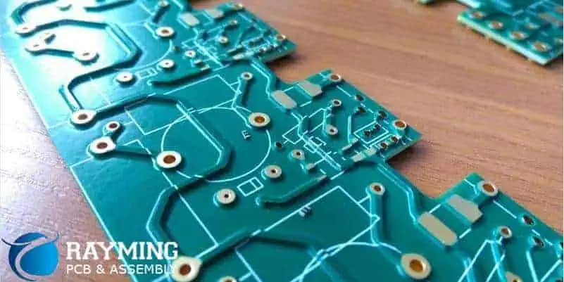
Before delving into optimization techniques, it’s essential to understand what constitutes a high current PCB in the context of motor controls. Generally, PCBs handling currents above 10A are considered high current boards. However, in motor control applications, currents can often exceed 100A or more, depending on the motor size and application.
Challenges in High Current PCB Design
Designing PCBs for high current motor control presents several challenges:
- Heat generation and dissipation
- Voltage drops across traces
- Electromagnetic interference (EMI)
- Mechanical stress due to thermal expansion
- Component selection and placement
- Safety and reliability concerns
Addressing these challenges is crucial for creating an optimized high current PCB for motor controls.
Key Design Considerations
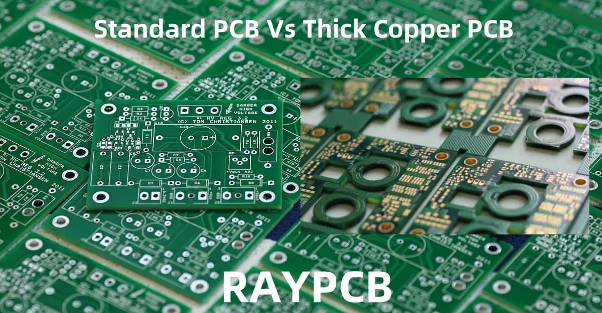
Copper Weight and Thickness
One of the most critical factors in high current PCB design is the copper weight and thickness. Increased copper thickness allows for higher current-carrying capacity and better heat dissipation. Common copper weights for high current applications include:
| Copper Weight (oz) | Thickness (μm) | Typical Current Capacity |
| 1 oz | 35 μm | Up to 10A |
| 2 oz | 70 μm | 10A – 20A |
| 3 oz | 105 μm | 20A – 30A |
| 4 oz | 140 μm | 30A – 40A |
| 6 oz | 210 μm | 40A – 60A |
For very high current applications, even thicker copper (up to 10 oz or more) may be necessary.
Trace Width Calculation
Proper trace width calculation is crucial for ensuring that PCB traces can handle the required current without overheating. The IPC-2152 standard provides guidelines for determining trace widths based on current, temperature rise, and copper thickness. Here’s a simplified table for quick reference:
| Current (A) | Trace Width (mm) for 10°C Rise (1 oz Cu) | Trace Width (mm) for 20°C Rise (1 oz Cu) |
| 1 | 0.2 | 0.1 |
| 5 | 1 | 0.5 |
| 10 | 2.5 | 1.3 |
| 20 | 6.4 | 3.3 |
| 50 | 22.9 | 11.7 |
Note: These values are approximate and should be verified using PCB design software or IPC-2152 calculators for specific applications.
Layer Stack-up Optimization
Optimizing the layer stack-up is essential for managing high currents effectively. Consider the following strategies:
- Use thicker outer layers for improved heat dissipation
- Dedicate entire layers to power and ground planes
- Implement a symmetrical stack-up to minimize board warpage
- Use multiple layers in parallel for very high current paths
Thermal Management
Effective thermal management is critical in high current PCBs for motor controls. Implement the following techniques:
- Use thermal vias to conduct heat from components to internal or bottom layers
- Implement copper pour areas for improved heat spreading
- Consider using metal-core or insulated metal substrate (IMS) PCBs for extreme heat dissipation requirements
- Strategically place high-power components to optimize heat distribution
EMI Reduction Techniques
Minimizing electromagnetic interference is crucial in motor control applications. Implement these EMI reduction strategies:
- Use a ground plane to provide a low-impedance return path
- Implement proper component placement to minimize loop areas
- Use EMI suppression components such as ferrite beads and common-mode chokes
- Consider shielding techniques for sensitive circuits
Component Selection and Placement

Power Components
Selecting appropriate power components is crucial for high current motor control PCBs. Consider the following factors:
- Current rating: Choose components rated for the maximum expected current with a safety margin
- Voltage rating: Ensure components can withstand the maximum voltage in the system
- Thermal characteristics: Select components with low thermal resistance and adequate heat dissipation capabilities
- Footprint: Consider the PCB real estate required for each component
Driver ICs and MOSFETs
For motor control applications, driver ICs and MOSFETs are critical components. When selecting these components, consider:
- Switching frequency: Choose components capable of operating at the desired switching frequency
- Gate charge: Lower gate charge MOSFETs reduce switching losses
- On-resistance: Lower on-resistance MOSFETs reduce conduction losses
- Thermal performance: Select components with good thermal characteristics and consider using additional heatsinks if necessary
Capacitor Selection
Proper capacitor selection is essential for filtering and stabilizing the power supply in motor control circuits. Consider the following:
- Capacitance value: Choose capacitors with appropriate values for filtering and decoupling
- Voltage rating: Ensure capacitors can withstand the maximum voltage in the system
- ESR (Equivalent Series Resistance): Select low-ESR capacitors for improved performance
- Ripple current rating: Choose capacitors with adequate ripple current ratings for the application
Component Placement Strategies
Optimal component placement is crucial for high current PCBs. Follow these guidelines:
- Place power components close to each other to minimize trace lengths
- Use symmetrical layouts for parallel components to ensure even current distribution
- Keep sensitive control circuits away from high current paths
- Consider the direction of current flow and heat dissipation when placing components
PCB Layout Techniques
Power and Ground Plane Design
Proper power and ground plane design is critical for high current PCBs. Implement the following techniques:
- Use solid power and ground planes whenever possible
- Minimize splits in power and ground planes
- Use star-point grounding for sensitive analog circuits
- Implement separate power and ground planes for digital and analog sections
Trace Routing Strategies
Effective trace routing is essential for managing high currents. Consider these strategies:
- Use wide, short traces for high current paths
- Implement multi-layer routing for very high currents
- Avoid 90-degree turns in high current traces; use 45-degree or curved traces instead
- Keep high current traces on outer layers for better heat dissipation
Thermal Relief and Stitching Vias
Implement thermal relief and stitching vias to improve heat dissipation and current distribution:
- Use thermal relief patterns for component pads connected to large copper areas
- Implement stitching vias to connect copper pours on different layers
- Use an array of vias for high current connections between layers
Design for Manufacturability and Testing
DFM Considerations
Design for manufacturability (DFM) is crucial for ensuring that high current PCBs can be produced reliably. Consider the following DFM guidelines:
- Maintain minimum clearances between high current traces and other elements
- Ensure adequate spacing between components for assembly and rework
- Use standard drill sizes and avoid blind and buried vias if possible
- Implement fiducial marks for automated assembly
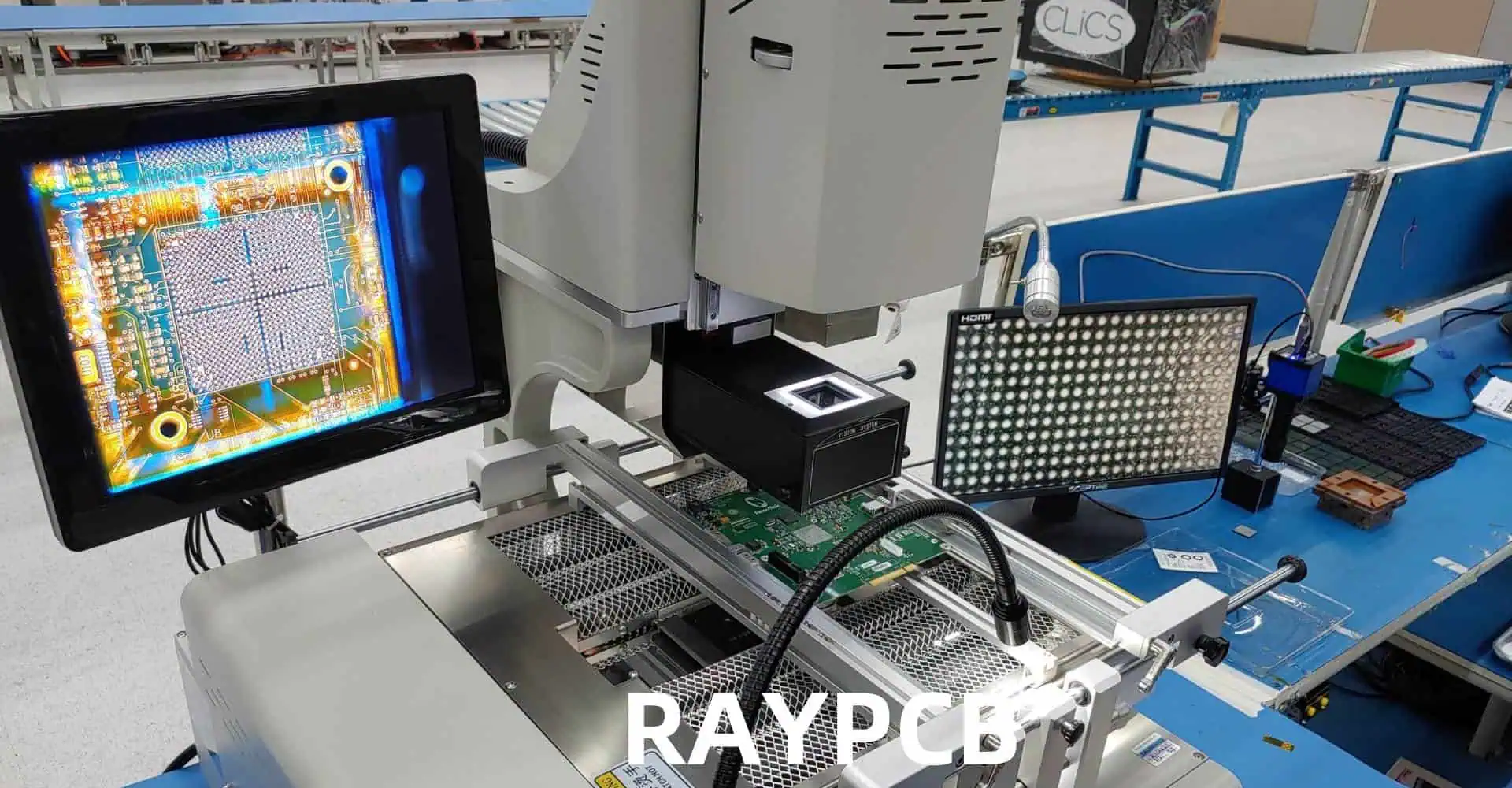
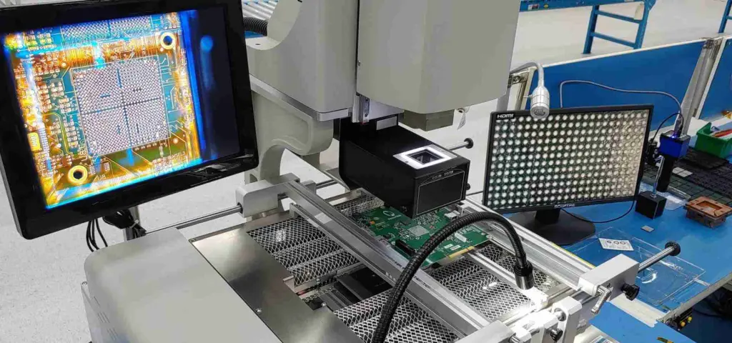
Testing and Verification
Proper testing and verification are essential for ensuring the reliability of high current PCBs. Implement the following strategies:
- Design in test points for critical signals and power rails
- Consider implementing boundary scan (JTAG) for improved testability
- Plan for in-circuit testing (ICT) if required
- Implement thermal sensors for monitoring during operation
Safety and Regulatory Considerations
Creepage and Clearance
Ensuring adequate creepage and clearance distances is crucial for safety in high current PCBs. Consider the following:
- Maintain appropriate creepage distances based on voltage levels and pollution degree
- Ensure sufficient clearance between high voltage nodes and other circuits
- Use slot cuts or grooves to increase creepage distance when necessary
Regulatory Compliance
Ensure that your high current PCB design complies with relevant safety and regulatory standards, such as:
- IEC 60950-1 for IT equipment safety
- UL 508C for industrial control equipment
- IEC 61800-5-1 for adjustable speed electrical power drive systems
Case Studies
Case Study 1: High Power Motor Drive for Electric Vehicle
A PCB designer optimized a motor drive board for an electric vehicle application with the following specifications:
- Motor current: 300A peak
- Supply voltage: 400V DC
- Switching frequency: 20 kHz
Key optimizations included:
- Use of 6 oz copper for main power traces
- Implementation of a 10-layer PCB with dedicated power and ground planes
- Use of parallel MOSFETs with optimized gate drive circuits
- Implementation of a liquid cooling system for thermal management
Results:
- 25% reduction in PCB size compared to previous design
- 15% improvement in overall system efficiency
- Successful operation in harsh automotive environments
Case Study 2: Precision Motor Control for Industrial Robotics
A designer optimized a PCB for a precision motor control application in industrial robotics:
- Motor current: 50A continuous
- Supply voltage: 48V DC
- Position feedback resolution: 0.1 arc-second
Key optimizations included:
- Use of a 4-layer PCB with 2 oz copper for power layers
- Implementation of star-point grounding for sensitive analog circuits
- Use of local power filtering for each drive stage
- Implementation of EMI reduction techniques, including ground planes and ferrite beads
Results:
- 40% reduction in position jitter compared to previous design
- 30% improvement in overall system accuracy
- Successful operation in noisy industrial environments
Conclusion
Optimizing high current PCBs for motor controls requires a comprehensive approach that addresses thermal management, EMI reduction, component selection, and layout techniques. By implementing the strategies and best practices outlined in this article, designers can create efficient, reliable, and high-performance motor control systems that meet the demands of modern applications.
As motor control technology continues to advance, the importance of optimized high current PCB design will only increase. Staying up-to-date with the latest design techniques, materials, and components will be crucial for engineers working in this field. By carefully considering all aspects of high current PCB design, from initial concept to final testing and verification, designers can create motor control systems that push the boundaries of performance and reliability.
Frequently Asked Questions (FAQ)
Q1: What is the maximum current that can be safely carried on a PCB trace?
The maximum current capacity of a PCB trace depends on several factors, including copper thickness, trace width, ambient temperature, and acceptable temperature rise. There’s no fixed maximum, but as a general guideline:
- 1 oz copper traces can typically handle up to 10A with proper width and thermal management
- 2 oz copper traces can handle up to 20A
- 4 oz copper traces can handle up to 40A
- For currents above 50A, it’s common to use multiple layers or copper bars
Always use IPC-2152 standards or PCB design software to calculate exact current capacities for your specific design requirements.
Q2: How can I reduce EMI in high current motor control PCBs?
To reduce EMI in high current motor control PCBs, consider the following techniques:
- Use a solid ground plane to provide a low-impedance return path
- Minimize loop areas in high current paths
- Use differential signaling for sensitive signals
- Implement proper component placement to separate noisy and sensitive circuits
- Use EMI suppression components like ferrite beads and common-mode chokes
- Consider shielding techniques for sensitive circuits
- Use snubber circuits to reduce ringing in switching circuits
- Implement proper filtering on power inputs and outputs
Q3: What are the advantages and disadvantages of using thicker copper for high current PCBs?
Advantages of thicker copper:
- Higher current-carrying capacity
- Better heat dissipation
- Lower voltage drop across traces
- Potentially fewer layers required for high current paths
Disadvantages of thicker copper:
- Higher material costs
- More difficult to etch fine traces and spaces
- Increased overall PCB thickness
- Potential for greater thermal expansion mismatch
- More challenging to achieve impedance control for high-speed signals
Q4: How do I choose between using wider traces or multiple layers for high current paths?
The choice between wider traces and multiple layers depends on several factors:
- Available PCB space: If space is limited, multiple layers may be more efficient
- Current requirements: Very high currents may necessitate both wide traces and multiple layers
- Thermal considerations: Multiple layers can provide better heat distribution
- Impedance control: Wider traces may impact impedance-controlled lines on the same layer
- Cost: Adding layers increases PCB cost, while wider traces on existing layers may be more economical
- Manufacturability: Very wide traces can be challenging to etch consistently
Generally, for currents up to 20-30A, wider traces on a single layer are often sufficient. For higher currents, a combination of wide traces and multiple layers is typically more effective.
Q5: What are the key considerations for thermal management in high current motor control PCBs?
Key thermal management considerations for high current motor control PCBs include:
- Copper thickness and trace width: Use thicker copper and wider traces for better heat dissipation
- Layer stack-up: Optimize layer stack-up for heat distribution, using thicker outer layers
- Thermal vias: Implement thermal vias to conduct heat from components to internal or bottom layers
- Copper pours: Use large copper areas for improved heat spreading
- Component placement: strategically place high-power components to optimize heat distribution
- Cooling solutions: Consider using heatsinks, fans, or even liquid cooling for high-power designs
- Thermal simulation: Use thermal simulation tools to identify and address hotspots
- Material selection: Consider using high thermal conductivity PCB materials for better heat dissipation
- Power plane design: Implement solid power planes for improved heat distribution
- Thermal reliefs: Use thermal relief patterns for component pads connected to large copper areas to balance heat dissipation and solderability