When multiple capacitors are connected in series in a circuit, their individual capacitances combine to act as an equivalent net capacitance across the overall string. The total capacitance in a series circuit is always less than the smallest capacitor in the chain.
Understanding how to calculate the equivalent capacitance for capacitors in series is key to properly designing and analyzing circuits containing series-connected capacitors. In this guide, we will cover:
How series capacitors behave in AC and DC circuits
Rules to calculate net capacitance in series strings
Gaining a robust knowledge of the principles governing capacitors in series will provide you the ability to optimize capacitor banks for filters, timing circuits, voltage dividers, and other applications. Let’s start by reviewing the fundamentals.
A capacitor consists of two conducting plates separated by an insulating dielectric material. When a voltage differential exists between the plates, an electric field forms across the dielectric which stores charge.
The capacitance (C) depends on the plate area (A), dielectric thickness (d), and dielectric constant (εr):
C = εr*A/d
Key capacitor behaviors:
Opposes changes in voltage
Stores energy in electric field
Can pass high frequencies but blocks DC
Charges and discharges over time
Now let’s examine how these properties combine when capacitors are connected in series.
Capacitors in Series – AC Behavior
When AC voltages are applied across a string of series capacitors, the alternating current can pass through each capacitor freely.
In AC circuits, series capacitors look like a single equivalent capacitor with a capacitance equal to the lowest value capacitor in the chain. This makes sense intuitively – the smallest capacitor will impede the AC the most, so it determines the overall impedance.
For example, for 10nF, 22nF and 47nF capacitors in series:
The 10nF capacitor has the least capacitive reactance
This capacitor’s impedance limits the AC through the chain
So the series string acts like a single 10nF capacitor
Modeling the series capacitors as a single equivalent capacitor is an effective AC circuit analysis technique. But this model does not hold true for DC conditions.
Capacitors in Series – DC Behavior
Direct current cannot pass through a capacitor – it becomes an open circuit. So what happens for DC applied to series capacitors?
With DC voltage applied, each capacitor in the series chain charges up to the applied voltage. Essentially, each capacitor acts like its own individual voltage divider.
The key observations:
Each capacitor charges up to the same DC voltage
The series string blocks direct current
The equivalent capacitance decreases compared to a single capacitor
This equivalent capacitance decrease follows specific rules…
Rules to Calculate Equivalent Capacitance
To find the net equivalent capacitance of capacitors in series, two key rules apply:
Rule 1: Net Capacitance Decreases
The overall capacitance of a series string is always less than the smallest capacitor:
Ceq < Cmin
For example, 10nF, 22nF, and 47nF capacitors in series always results in:
Ceq < 10nF
This matches the AC behavior where the smallest capacitor determines the impedance. But for DC, the exact Ceq formula follows the next rule…
Rule 2: Reciprocal Summation
The total capacitance for series capacitors is calculated using:
1/Ceq = 1/C1 + 1/C2 + 1/C3 ...
Where C1, C2, C3, etc. are the individual capacitances
Applying this reciprocal summation rule to a series string of:
10nF + 22nF + 47nF
Gives:
1/Ceq = 1/10nF + 1/22nF + 1/47nF Ceq = 7.48 nF
So connecting these three capacitors in series results in an equivalent capacitance of 7.48nF, always less than the smallest capacitor.
This reciprocal summation formula allows calculating the net capacitance of any series combination. Understanding these fundamental rules is key to working with series capacitor circuits. Next let’s look at the equivalent circuit model.
Equivalent Circuit Model
Based on the capacitance rules, the standard equivalent circuit model for any series capacitor combination replaces the chain with a single capacitor:
Where:
Ceq is the equivalent capacitance calculated from the reciprocal summation of individual capacitances
RLeak is the insulation resistance representing leakage through the dielectric
This model allows applying simpler capacitor formulas for analyzing series chains in circuit simulations or calculations.
Note that while this model holds for DC conditions, simply using the smallest capacitor value directly can suffice for AC-only analysis as mentioned earlier.
Now let’s examine how the voltage divides across series capacitors…
Because series capacitors all charge up to the total applied voltage, the voltage divides proportionally across each capacitor depending on their capacitive reactance.
VC1, VC2, etc. are the voltages across each capacitor
XC1, XC2, etc. are the capacitive reactances
VTotal is the total voltage applied to the series string
The capacitor with the lowest capacitive reactance receives the highest voltage.
This voltage division characteristic is important when specifying capacitor voltage ratings in a series circuit. The capacitor with the smallest value must have a voltage rating exceeding the total applied voltage.
Now let’s look at some examples of using series capacitors.
Applications of Series Capacitors
Some common applications that leverage series capacitor behaviors:
AC Coupling and DC Blocking
Connecting a series capacitor allows an AC signal to pass while blocking the DC component. This AC coupling is useful for isolating stages:
C1 passes the AC input signal but blocks DC from reaching the amplifier. R1 slowly discharges C1.
Voltage Transformation in Power Systems
Connecting high voltage ceramic capacitors in series allows creating a string to withstand very high voltages for power electronic applications and transmission grids.
High Voltage DC Link for Inverters
Stacking film or electrolytic capacitors in series enables creating a high voltage DC bus for feeding inverters that require very high DC voltages:
Timing Circuits
Combining different capacitor values in series provides an RC time constant that can be used for timer and oscillator circuits.
These examples highlight applications where connecting capacitors in series supports key design goals. But series capacitors also introduce potential issues that engineers should be aware of…
Troubleshooting Issues with Series Capacitors
While connecting capacitors in series has benefits, some problems can emerge that require mitigation:
Voltage Spikes from Mismatched Values
If the capacitor voltage ratings are mismatched, the lowest rated capacitor may experience overvoltage spikes and get damaged. Always check division with ratings.
Unbalanced Voltage Sharing
Differences in leakage currents or capacitor aging can lead to uneven voltage division, overstressing one capacitor. Voltage balancing resistors helps mitigate this.
Open Capacitor Faults
An open fault on one capacitor will shift more voltage onto the remaining capacitors, potentially exceeding their rating. Protection circuits should detect and respond to open faults.
Properly sizing components and implementing monitoring helps prevent these common modes of failure in series capacitor banks and strings.
Conclusion
In summary, the key rules when working with capacitors in series are:
AC signals only “see” the smallest capacitance
DC cannot pass, so equivalent capacitance decreases
Equivalent capacitance uses the reciprocal summation formula
Voltage divides according to the capacitive reactance
Carefully applying these principles allows you to properly analyze, design, and troubleshoot circuits utilizing series capacitors in filter networks, timing circuits, voltage dividers, and other applications.
Frequently Asked Questions
How is total capacitance calculated for capacitors in series?
Use the reciprocal summation rule: 1/Ceq = 1/C1 + 1/C2 + 1/C3… This gives the equivalent capacitance for a series combination.
Why is capacitance less when capacitors are in series versus parallel?
In series, capacitors charge to the same voltages so their fields oppose and capacitance decreases. In parallel, the fields sum because the caps share the same voltage.
How does capacitor voltage divide across a series string?
Voltage divides according to the capacitive reactance (XC). The lower XC capacitor has more voltage across it.
When should you use series capacitors versus parallel capacitors?
Use series to decrease net capacitance and withstand high voltages. Use parallel to increase capacitance for higher charge storage.
How do you calculate impedance for capacitors in series?
You can simply use the value of the smallest capacitor in the series string to model the AC impedance, since it limits current flow.
If you’ve been searching for some reliable information about the inverter PCB, then you will find reliable answers here.
Our article will cover the important things you should know about inverter PCB. Therefore if you wish to gain vast knowledge on the topic, please continue reading.
What are Inverter PCBs?
These are printed circuit boards, which convert DC (direct current) into AC (alternating current). They are usually manufactured with great performance. Furthermore, as a result of their layered design, inverter printed circuit boards are greater in contrast to other PCBs, although they all serve the same functions.
Inverter PCBs save much space, coupled with lessening the board weight. In addition, it features increased durability, lightweight construction, and better flexibility.
This PCB is great for data storage, Bluetooth, air conditioner, computers, and more. Therefore, if you’re an electrical engineer, product designer, system integrator, searching for high-quality inverter pcbs, then you can work with RayMing PCB.
Inverter pcbs are known to form the important parts of today’s electronic equipment. Furthermore, it features some passive and active component connections. So, these PCBs have these benefits.
Saves wire via its compact size
As a result of copper tracks’ presence substituting different wire types, inverter printed circuit boards feature compact sizes. Explaining further, wires take a large space on inverter PCBs, which may lead to size increase.
Diagnosing and Repairing is Easy
Anytime the inverter PCB malfunctions, identifying the problem becomes very easy. Asides from this, you won’t have to spend so much either on personnel or resources in replacing the part with a problem.
Saves Time
When assembling the parts of an inverter pcb, you’ll save much time. In contrast to conventional circuit connection methods, connecting your inverter PCB makes use of machines requiring high tech. This reduces the cost of labor and saves you time, which you can easily invest on other projects.
Prevents Frequent Movement
All the inverter PCB parts hold onto the board tightly. Therefore, this prevents movement of any form. This makes the movement of the device easy without the feat of bringing damages on your product.
Low Noise
Inverter PCBs are one of the most silent devices, which don’t produce much electronic noise. With the right connections, inverter PCBs have the ability of reducing electronic noise production.
Inverter printed circuit boards are useful in different applications and fields. Below are the major applications of inverter pcbs.
Lighting Applications
Inverter printed circuit boards are useful in any lighting application to produce LED lights. Today, they are becoming more popular. Furthermore, they aid better the manufacturing of aluminum and LED backed lights by serving as the main heat and heat sync outlets.
Industrial Machines
Inverter PCBs are important in the industrial machine. This is mainly to assist in converting proper circuits properly. This also aids in reducing the industrial machineries, therefore occupying lesser space and making it lighter overall.
Medical Industry
High-density inverter PCBs are usually present in the majority of medical devices. This makes them very small in size. With this feature, it takes away the headache of reducing the weight and size of medical devices.
In order to make very sophisticated and accurate devices to work in the automotive industries, you will have to depend on inverter PCBs. This is one good reason why the majority of automobiles and cars possess this ability of functioning better when they have new and reliable devices.
Inverter PCBs come in three major types which you can choose from. Here they are.
Single Sided Inverter PCB
The single layer or single sided inverter PCB possesses just a layer of material or base substrate. It possesses just one copper coating layer on one of its sides, which is followed by a silkscreen or solder mask for making the elements out.
Asides from this, it possesses all the necessary components, which makes the circuit on a side, therefore making it easy to manufacture and design.
Double Sided Inverter PCB
The double layer or double sided inverter pcbs have copper metals on the two sides of its base plate. Furthermore, holes are present on both boards, which links the circuit present on one of the sides to the other side’s circuit.
The inverter PCB’s components can be connected via the through-holes or surface mounting. This type of PCB should be used on applications having a middle complexity level like power supplies.
Specifications to Consider before choosing the Right Inverter PCB
Whatever inverter PCB you choose should vary, which is based on some factors. Let’s consider them.
Thermal Expansion
Make use of materials having the same rate of thermal expansion. This helps in avoiding losses as a result of temperature differences.
Dielectric Loss
Check the signal transmission’s quality, which is necessary for your applications. This means that you should go for inverter printed circuit boards having very little or zero dielectric loss. This is to prevent signal wastages.
Water Absorption
Also, check for the rate of water absorption because they can also affect both the PCB’s dielectric constant and dielectric loss.
If you will be making use of an inverter PCB in a wet environment, make sure that your PCB’s components have what it takes to withstand any effect.
Other Resistances
Asides from the properties above, ensure that the materials you are using for the construction of the inverter PCB have high ratings. Also, make sure that these components are very resistant to hazardous chemicals and heat. Also it must possess the perfect endurance and impact.
Conclusion
We hope we have been able to explain what the Inverter PCB is all about. These are the major points you should know. If you have a question concerning the topics, please contact us.
PCB assembly drawing is one step in the PCB assembly procedure that you cannot skip. The process can be pretty tedious, especially when carrying it out manually. But before we move on to the complexity of the process, what does PCB Assembly Drawing entail? Why is this step crucial? And how can we make PCB Assembly Drawing easier to tackle? To get the answers to these questions, follow along to learn more.
What exactly is PCB Assembly Drawing?
Have you ever heard of PCB Assembly Drawing? Have you ever tried out PCB Assembly Drawing? If your answer to any of these questions is no, worry not because we are here to solve your mysteries. See, PCB Assembly Drawing is the presentation of a product or structure with its components connected to it. The components that connect to the main structure all undergo different fabrication processes. The assembly and installation of these components is such that all components fit and match with each other. They should all work harmoniously for the complete gadget to function right. Therefore messing up this drawing could make the PCB not function properly.
Most people confuse PCB Assembly Drawing with PCB Fabrication Assembly Drawing. Do you know the difference between the two? Well, if not, then here is the answer. See, Fabrication PCB Drawings contains data on how to build the PCB. On the other hand, the PCB assembly drawing shows how various components connect to the RAW print circuit board. These two drawings are crucial. However, they do not play the same role in PCB assembly.
To see the difference between these two drawings, let us look at some components found in a fabrication drawing:
Dimensions – helps identify project material quantity. Dimensions include:
The board’s length and width
Thickness of the boards
The board’s outline
Tolerance
Hole charts – outlines parts that need special care
Layer stack-up – influences project characteristics directly. For example impedance requirement handling varies according to material thickness stack up tolerance and thickness
PCB Assembly Drawing, Basics
Generic Items that are Crucial to PCB Assembly Drawing
Generating a PCB drawing follows some guidelines. These guidelines help standardize the process of generating PCB drawings. If you are looking to make a PCB Assembly Drawing, then here are some generic items that you should include:
Drawing Format – Some CAD PCB Drawing systems will prompt you to use drawing formats found in the system’s library. However, other systems will simply auto-generate the drawing format for you. In either case, you will combine the drawing format and your PCB’s layout to generate your drawing.
Board Outline – The board outline simply represents the PCB design outline from your layout database. In most cases, the board outline will include:
These two components appear on the fabrication drawing, whereby the dimensions are set. On the other hand, when the drawing reaches the PCB Assembly Drawing stage, referencing of these components occurs.
Identification Information – Your drawing format should have some areas on it that you should utilize to:
Add in the drawing’s identification number
It’s revision level
The board’s name
The corporates address
Contact data
The creation date
All this information helps uniquely identify your PCB, which is pretty crucial.
Key PCB Assembly Drawing Elements
Component outlines
While making a PCB assembly drawing, you will want to display:
Every component’s shape
Reference designators for the components in your drawing as per how soldering will occur in this particular board.
You should also include the mechanical parts which connect onto the board using mounting hardware. In some cases, you might need to add more effort to include these parts in your drawing. That is because the CAD footprint library sometimes does not have accurate representations of these parts. So you must go in manually.
Additional Views
Double-sided boards need a back view drawing and a front view drawing. These two sides can fit inside a single drawing sheet as long as the board is not large. However, if the board is large, you might need to use extra drawing sheets to cover the entire drawing.
You might also need to add an expanded view, which contains detail on the mechanical part’s connection for clarity.
Manufacturing Labels
If you include any manufacturing label, for example:
An assembly tag
Barcode
Then you must pinpoint it using a pointer. After identifying it, you then reference it in your notes. Anyone looking for it can easily identify it without straining a lot.
Assembly Notes
Is a list that features manufacturing instructions such as:
Assembly details
Industry standards
Specifications
Special feature locations
Assembly notes sometimes include a list of parts, but only when manufacturers request it.
All these elements can be modified to fit the specifications of a client. You can even omit some of these elements entirely if you feel like they do not apply in your client’s drawing.
When it comes to choosing the right elements to use in your drawing, you should consult your contract manufacturer. They will tell you what they require to generate your PCB. In doing so, you get to avoid repeating an entire PCB Assembly Drawing.
Traditional PCB Assembly drawing tools were not superb in drafting capabilities. In fact, in most cases, people had to draft drawing by hand, which was a lot of work. However, those horrifying days are over. Now, modern-day PCB Assembly Drawing systems can generate impressive drawings automatically.
If you are using a traditional PCB Assembly Drawing system, we suggest updating it because you are missing out on a lot. Modern-day systems utilize special software which drafts out your drawing in a matter of minutes. Doing so saves you a lot of time and, ultimately, a lot of stress.
What’s more, this system is more accurate when comparing it to using freehand. This is because human errors are to the absolute minimum, which means that accuracy is almost always guaranteed.
To find modern-day PCB assembly drawing systems, simply search online and choose the one that favors you. Most of them have impressive user interfaces; hence using them is pretty easy.
Conclusion
PCB Assembly drawing is pretty crucial in the PCB assembly process. You should hence be extra careful when dealing with this step. Remember that your contractor generates your PCB according to your drawing. Therefore, omitting an element or a component can be catastrophic. However, if you follow the tips in this article, then the chances of messing up your PCB assembly drawing go down.
Mini water pumps provide an inexpensive and educational method to learn about fluid pumping fundamentals. Building your own small pump enables experimenting with mechanical designs, testing performance, and understanding the physics of pumping.
This guide covers the process of constructing a miniature water pump using easily obtained materials. We will look at:
Constructing your own mini pump is an engaging hands-on project that also teaches you the engineering physics and practical knowledge to develop real-world pumping solutions. Let’s get started!
Before we build a mini pump, it helps to understand the operating principles that enable pumping:
Reciprocating Pump Overview
While many pump types exist, we will build a reciprocating piston pump for this project. Reciprocating pumps use a piston in a cylinder to provide pulsating flow.
The powered reciprocating motion produces suction and discharge strokes:
Suction Stroke
Piston retracts, inlet valve opens
Low pressure draws fluid into cylinder
Discharge Stroke
Piston advances, inlet valve closes
High pressure pushes fluid out outlet valve
This cyclic action produces overall fluid flow.
Creating Suction Through Pressure Differentials
The key principle that enables pumping is creating localized low pressure (suction) to force flow into the pump.
For liquids, pressure and fluid flow are directly linked through Bernoulli’s principle. By forming an area of low pressure, higher pressure regions will force liquid to move to the lower pressure zone.
In a pump, the moving piston lowers pressure in the cylinder on the inlet stroke. The higher pressure of the fluid supply then pushes fluid into the cylinder through the open inlet check valve.
Understanding this pressure differential concept helps explain how pump suctionlift works. Now let’s look at constructing a mini pump!
Materials and Parts Needed
We will build the pump using easily obtained hardware store parts:
Once assembly is complete, testing the pump involves:
Checking for air leaks with manual operation
Priming the cylinder
Powering the motor at low voltage
Gradually increasing voltage while observing function
Safety first – wear eye protection in case of parts coming loose at higher speeds.
Let’s look at the process:
Check for Air Leaks
Manually reciprocate the magnets using the motor. Listen for any audible air hissing that indicates an end cap leak.
If leaks occur, try re-sealing with additional silicone sealant or wrap the threads with Teflon tape.
Prime the Cylinder
Initially fill the cylinder with water through the inlet before attaching the intake tube.
This provides the initial fluid volume needed to fill voids and enable pumping.
Power Motor at Low Voltage
Connect the motor terminals to a variable benchtop power supply set to 3-5V.
Power the motor to begin slow reciprocation and pumping.
Gradually Increase Voltage
Slowly increase the supply voltage while observing pump operation.
Aim to achieve maximum stroke rate without the magnets impacting the cylinder ends.
Check Flow Rate
Once operating, compare the inlet and outlet flow rates by pumping into a graduated container.
This verifies the pump is working.
Adjusting the stroke length and motor RPM provides insight into the physics. Now let’s look at some experiments to try.
Experiments and Learning
Building your own mini pump enables exploring pumping physics and engineering in several ways:
Flow Rate vs. Speed
Record flow rates at different motor RPM settings. Plot the relationship.
Faster stroking increases flow following the affinity laws.
Suction Lift vs. Stroke Rate
Test maximum suction lift by raising the inlet reservoir.
See how rapidly air entrains at higher lifts as speed increases.
Power Consumption
Monitor current draw of the motor across operating conditions.
Calculate input power and pumping efficiency.
Analytical Modeling
Build a mathematical model of the pump based on physics principles.
Compare predictions to measured data to validate model accuracy.
Component Changes
Try different cylinder materials like steel or plastic.
Modify piston seals and bearing surfaces.
Adjust magnet size and stroke lengths.
Building a physical working system enables learning through experimentation and observation that textbooks or simulations cannot achieve alone. Gaining first-hand practical knowledge of fluid pumping principles through your mini pump will prove valuable if you ever design industrial-scale systems.
Now that you have experienced small-scale pumping, let’s look at how these learnings apply to real-world systems.
Scaling Up Designs
While mini water pumps operate on milliliters per minute, applying these fundamentals allows engineers to design pumps moving thousands of gallons. Let’s examine how the principles scale:
Reciprocating Pump Scalability
Single piston pumps can scale from watts to megawatts of power.
Multi-piston designs provide flexibility for capacity and pressure needs.
Stroke length dictates displacement per cycle.
Standardized power transmission components are available.
Creating Suction Head
Same principle of localized low pressure applies at all scales.
Just as with the mini pump, the affinity laws relating
Flow, head, power and RPM apply to industrial pumps.
Guidelines for velocity and pressures remain valid.
Performance scales predictably with linear dimensions.
The core operating physics remains unchanged. An experiential understanding of pumping from building a mini pump provides intuition applicable to real installations.
Conclusion
Constructing your own mini water pump is an enlightening hands-on engineering project. The key takeaways are:
Pumps create flow by generating suction through pressure differentials
Reciprocating pumps produce pulsating flow from cyclic pistons
A custom pump can be built from easily obtained hardware materials
Principles scale directly to industrial pumping systems
Gaining first-hand experience with the practical aspects of pumping makes physics and engineering principles more intuitive. Mini pumps provide great insight into fluid system fundamentals.
Frequently Asked Questions
What is the best size cylinder to use for a mini pump?
1-2 inch diameters work well. Use the longest cylinder that fits your motor and magnets, typically 2-4 inches long.
What PSI pressure can a miniature pump generate?
Mini pumps generally produce less than 1 PSI. Pressure depends on cylinder size, RPMs, and outlet restrictions.
What causes a mini pump to lose prime during operation?
Air leaking into the cylinder, insufficient inlet pressure, or excessive stroke speed can break suction and lose prime.
How fast should a mini pump motor turn?
50-250 RPMs is ideal. Too slow reduces flow rate. Too fast causes inlet suction issues.
How can I increase the flow from my mini pump?
Use a larger cylinder, longer stroke length, faster motor RPMs, and reduce inlet and outlet restrictions.
When it comes to Electronic Assembly technicians, you can expect more than what meets the eye. For instance, did you know that you can earn an average annual salary of 33,218 USD as an electronic assembly technician? Breaking this down further, you get an average hourly salary of 15.97 USD. The job pays pretty well. But what does it entail? What responsibilities fall upon the shoulder of an electronic assembly technician? And what does it take to become an Electronic Assembly Technician? Well, follow along, and let us lead you along the path to success as an Electronic assembly technician.
What exactly does an Electronic Assembly Technician Job entail?
An electronic assembly technician carries out the following tasks:
Puts together electrical devices, tools, and equipment
Repairs electrical devices, tools, and equipment
Carries out tests on devices, tools, and equipment
The job description is pretty straightforward. However, the skill sets required to score this job widens up the job scope for people who have Electronic Assembly Technician skills. Due to this, some people might opt to work in different fields depending upon:
Personal preferences
Education
Electrical assembly Technicians might encounter hazardous equipment or materials. They, therefore, have to take extra precautions to shield themselves from harm.
Electronic Assembly Technician, Salary and Job Growth Rate
Becoming an Electronic Assembly Technician is not an easy feat. You have to weigh in many options that might help you make the right decision. However, some people go through a pretty tedious process to gain these options, which sometimes leaves them confused.
This section will look at some information that might help you make your decision without going through the tedious process.
First of all, let us look at the jobs growth rate. According to research, the job’s growth rate moves at a “slower than average speed.” We expect this job market to grow by an average of 3% in the next 10 years. This slow growth rate is mostly due to the automation of different procedures in this particular field. However, even with the automation issue, we still predict that by 2028, 1,100 job opportunities will have emerged from this sector.
Now let us move on to the salary part: The annual salary of an Electronic Assembly Technician is 33,218 USD on average. Breaking this down further, we get the average hourly pay of this job as 15.97 USD. However, this is an “average” breakdown. Looking at the actual number, we found that Electrical Technicians earn somewhere between 28,000 USD and 39,000USD. Therefore the gap between the low earners and high earners is roughly 11,000USD.
However, it is good to note that you are not restricted to this job alone with Electronic Assembly Technician skills. You can still choose another profession that requires Electronic Assembly Technician skill sets. For example:
Personality traits and skills to help you nail that Electronic Assembly Technician Job resume
Are you stuck in writing your Electronic Assembly Technician Job Resume? Here are some personality traits and skillsets that you can add to nail that resume in no time.
Assembly instructions
If you can operate and maintain assembly equipment, make sure you add this to your resume.
If so, add this to your resume. It will give you a shot at getting the job.
Surface mount
Assembling surface-mount circuits as per layout drawing using hand soldering under a microscope is not easy. Therefore if you can undertake this task, you should jot it down on your resume. It will give you an upper hand.
Customer requirements
Do you have experience in handling customer needs? Well, Electrical Assembly Technician jobs are all about handling client-specific instructions. Hence having this experience is another Ace up your sleeve.
Drill Press
Can you follow blueprints and mechanical schematics and use a drill press to assemble heat sinks for QC-laser and power supplies? Well, that is another star on your resume.
IPC
Do you have an IPC specialist soldering certificate? If you have the IPC certificate, do not leave it out when you include your resume attachments.
If you possess any or all of the skills described above, you might have a higher chance of getting this job. However, if you do not have this skill, then you can still learn them using simpler means, for example:
Through online classes
Via a tutor
By apprenticeship
As per personality traits, here are the most important ones to have to score this job:
Electrical Assembly Technicians should be able to understand and ultimately follow instructions. And in case they face any challenges, they should have the ability to communicate efficiently.
Creativity
Electrical Assembly Technicians help bring different electronic ideas to life. Hence, they should have a lot of creativity to handle different situations optimally.
Detail-oriented
Electrical Assembly Technicians have to follow specific customer instructions to develop devices. They hence have to be detail-oriented. Messing up one detail can ruin an entire order which could be catastrophic to the manufacturer.
Conclusion
Becoming an Electronic Assembly Technician is a process. It involves making many different decisions, some hard some not so much. Making this decision sometimes gets tough, but should you give up when things get tough. Well, no. We hope that this article has shone a light on the Electronic Assembly Technician job journey and what it entails. If you wish to undertake a job in this field, use the above instructions; you will get one within no time.
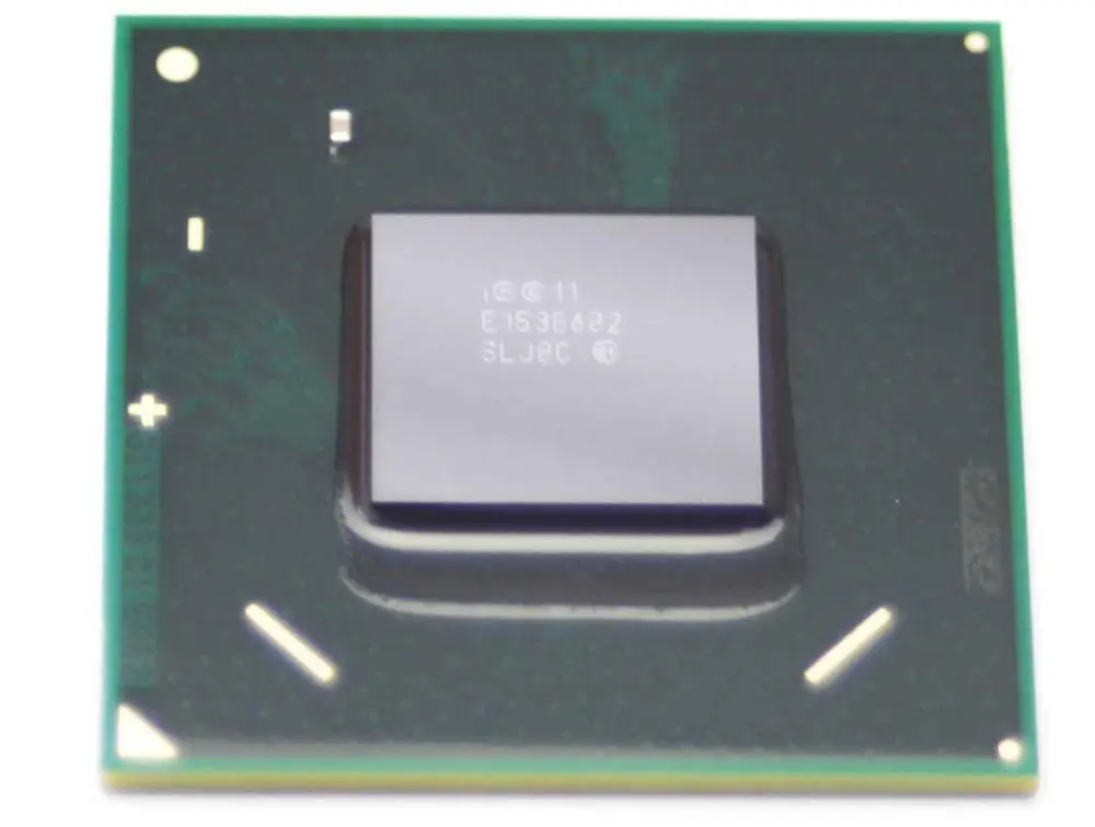
You’ve come to the right place if you’re looking for a good flipchip BGA. We will discuss TI’s BGA, Intel’s BGA, and Fujitsu’s TBGA. If you’re wondering what each one is and what they do, read on to learn more about these new packages. You’ll be surprised to know that these devices are so similar!
TI’s flipchip BGA
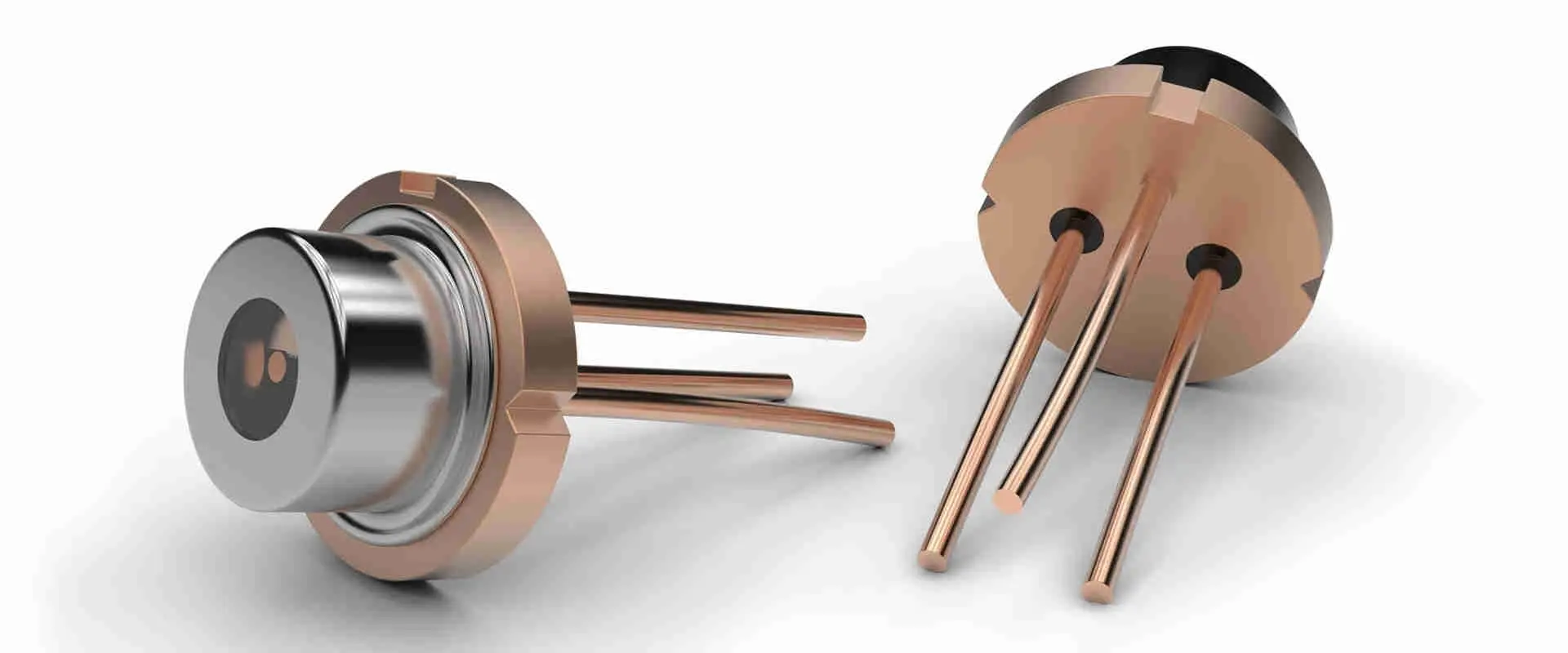
A BGA package is a low-profile semiconductor device consisting of a chip, interconnections, and a plastic encapsulant. These packages can be 1.2 mm in height and 0.05 inches wide and have a smaller loop area than QFP or SOIC, with equivalent pincounts. Smaller loop areas mean less crosstalk between pins and lower radiated noise.
The flip-chip BGA has many advantages, but it’s important to remember that it is not ideal for every application. For example, a high-frequency application may require a higher-frequency component. Flip chip packages also have better thermal conductivity and moisture resistance. The most common applications for flip-chip BGAs are semiconductor operations, but we can use them in detector arrays, passive filters, etc. You can read more about flip chip BGAs by clicking the link below.
The FlipChip Ball Grid Array is a high-performance and mid-cost solution for semiconductor packaging that uses controlled connection collapse chip technology. This process allows greater design flexibility and more signal density into smaller dies. As a result, it is an attractive choice when cost and performance are primary concerns. And unlike its wire-bond predecessor, we can mount and replace the FCBGA easily by following typical repair practices. In addition, it’s less complicated to install, and it can be hermetically sealed.
The high pin count, fine pitch, and high thermal dissipation requirements of today’s high-end logic devices enable the development of new packaging technologies such as TI’s Flip-Chip BGA. It achieves 1681 pin counts while minimizing crosstalk noise. The package uses a high-density organic substrate and Ni/Cu/Ti eutectic solder bump to achieve such results. TI’s Flip-Chip BGA package combines these characteristics with a flux-less bonding process for high reliability.
A vacuum head can lift the chip from a diced wafer. Next, the chip moves toward the BGA substrate through the die pick-up pin 60, which contacts the flip-chip solder bumps 22. Once we place the flip-chip on the BGA substrate, we attach the chip 30 by the solder bumps 22. Alternatively, we press and place the chip on the flip-chip substrate with the solder bumps facing up.
After placing the chip, we apply it to underfill the substrate. We then cure the underfill material during the solder bump reflow. This eliminates strict viscosity limits and improves production efficiency. Other improvements in underfill technology include fast-cure underfills and reworkable underfills. Rayming PCB & Assembly offers a list of underfill materials with their properties, applications, and recommended cure schedules.
In addition to being more flexible than conventional packages, BGAs have several other advantages that make them the preferred choice for high-end semiconductor designs. The most notable of these is the ability to use large amounts of solder balls without the risk of bridging adjacent pins. Moreover, flip-chip technology is easier to use and less expensive than its counterparts. Further, the process of soldering the BGA components is faster and more reliable, making it an excellent choice for highly complex electronics design.
Flip-chip BGA is an assembly method in which a single semiconductor chip sits on a flat or elevated surface. This method can be used in semiconductor manufacturing and is smaller in height and area than conventional BGA packages. Because the circuit board has no carrier, flip-chip assemblies allow higher-speed signals. The flip-chip also allows better heat conductivity. However, flip-chip assemblies must be arranged and maintained on flat surfaces, which is a significant drawback.
A flip-chip BGA package is similar to a QFP package, but the solder balls are different. They consist of a stronger material than conventional chips. The solder balls used in BGA are considerably thicker than QFP leads and can handle rough handling better than QFP. Intel uses flipchip BGA in the Atom brand. This new packaging method has many advantages over other forms of integrated circuit packaging.
Flip-chip BGAs is a mid-cost high-performance semiconductor packaging solution. This new technology utilizes a controlled collapse chip connection technology, a flip-chip. Flip-chip BGA provides greater signal density and functionality in a smaller die, making it an appealing choice for manufacturers seeking a balance between cost and performance. In addition, it is easy to mount and replace so that we can do the process in-house. However, the cost of manufacturing can be prohibitive for many manufacturers.
Fujitsu’s TBGA
TBGA is a type of package used to produce transistors. In this process, we package the transistors on a silicon substrate bonded to an organic buildup or BT substrate. This form factor allows manufacturers to control the electrical characteristics of the substrate, thereby reducing thermal resistance and V-G impedance. In addition, Fujitsu uses a metallic thermal injection method to eliminate voids and flatten the substrate.
The high-speed applications that benefit from a TBGA package include mobile phone chips, computer memory, and high-speed computing. TBGA packages are also available in various sizes, including the 32-bit SOT-32 package. Fujitsu’s TBGA flip-chip package offers many benefits over other technologies, including high speed and low inductance. Furthermore, this package provides excellent reliability, critical for many electronic applications.
Compared with other TBGA packages, the FC-PBGA can improve electrical, thermal, and mechanical properties. Therefore, FC-PBGA packaging is especially suitable for computing applications, as it is easier to manipulate than a conventional TBGA package. In addition, this type of package can increase the device’s reliability by improving the connections between the two sides. Further, it is easier to manufacture semiconductor dies in a large-scale package, as it is more robust.
A TBGA flipchip is another type of ball grid array. Unlike the conventional ball grid array (BGA), flip-chip BGA uses controlled collapse to connect chips. This works through solder bumps located on top of chip pads. Flip-chip BGA begins with a wafer of integrated circuits.
The latest advancement in CMOS packaging technology is TI’s CSP for flip-chip BGA packages. This packaging technology uses a conductive ball carrier that aligns over the BGA pads and is wetted, allowing the package to peel off and be soldered. This technique has several advantages, including reduced fanout and cost. As a result, the flip-chip BGA packages are widely applicable in ASIC, HPA, and DSP applications.
TI performs board-level reliability tests on its flip-chip BGA packages. First, the PCB land size must match the pad size of the flip-chip BGA package. Then, it uses flux and solder paste to attach the package to the PCB. This preconditioning shortens package development time, and reliability modeling provides an analytical tool for system performance and reliability analysis. After qualification testing, TI issues a list of packages with a netlist of their typical performance.
The useful life of a flip-chip BGA depends on the lifespan of the solder used to form the package. Therefore, TI’s methodology includes constant experimental verification and model refinement. Additionally, the CSP for flip-chip BGAs can be underfilled with epoxy powders because they’re cheaper than underfill fluid.
A significant challenge in flip-chip BGA packaging is determining how much epoxy is needed to fill the entire package. Conventional BGA packaging has a limited number of filler particles and a low CTE. The CSP for flipchip BGA uses a liquid or polymer underfill. This is an essential consideration for CSP packaging because it reduces the stress on the flip-chip BGA.
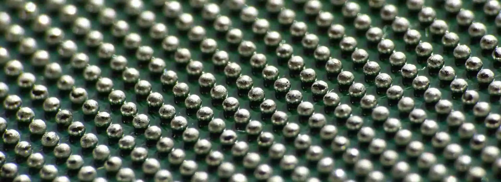
To make soldering balls, you can melt specks or pieces of hot crude oil. The upper portion of the column should be above the melting point, while the lower section should be below. Once the pieces melt, we can achieve the desired size by allowing them to cool in the viscous liquid. The soldering balls will retain their spherical shape unless oxides are present in the crude. To prevent such distortions, you can pour flux over the column.
Soldering spheres
The ALPHA HRL Series Lead-Free Solder Spheres are manufactured from patented lead-free alloys by Rayming PCB & Assembly. These spheres are available in various common diameters and are ideal for use with BGA and CSP components. In addition, XGR offers solder spheres in tape and reel formats on standard SMT equipment. Their low melting point ensures a uniform, clean, and safe soldering process.
We make these fluxless solder spheres with an online process that breaks the continuous laminar jet into uniform droplets. These droplets are then rapidly solidified in a liquid bath or inert gas. This process eliminates the need for a flux-based soldering flux and highly produces size-accurate solder microspheres.
The solder spheres consist of a material that bonds to pads and contact electrodes. Solder spheres also have a flexible material, which allows them to adjust their shape to block unwanted RF/EMI interference. A single sphere can bond up to six pads with a low melting point, while many spheres can be bonded together for maximum stability. Soilding spheres consist of silicon-based polymer, and their size is variable to match different conductive elements.
During soldering, the ball of solder squeezes away from the pad and does not coalesce during the reflow. The materials used, the size and type of components, the design rules of the stencils, and the characteristics of solder paste are all factors in the formation of these balls. This article will discuss the causes and possible remedies for mid-chip soldering balls.
To reduce mid-chip soldering balls, the size of the aperture is crucial. The smaller the aperture, the less solder goes onto the pad. In addition, the smaller the aperture, the lower the likelihood of mid-chip soldering balls. Therefore, a small aperture is better suited for high-volume chip soldering, as it reduces the amount of solder deposited on the pad.
Despite the small size, BGAs have numerous connections under their body. The gap between the BGA body and the PCB is only a few millimeters. Therefore, it is essential to achieve an even heat distribution underneath the BGA to solder these devices properly. Otherwise, one cold spot will cause the joint to be defective. Furthermore, since hot air cannot penetrate the narrow gap, solderers need to increase the package’s temperature and increase the time for it to heat.
A solder ball injection tool deploys a gas jet into the conductive sites. The process begins with the substrate pads placed in a fluidized ball reservoir. Next, the balls move into the conductive site with a coating. Another solder ball creation technique is known as a 3-Orifice design. This technique requires the use of solid solder alloy, preferably Sn63Pb37. Lead-free solder alloys are ideal for this method.
Stencil design
During SMT manufacturing, proper pad placement is essential for the success of your project. Incorrect pad placement may result in solder balls which may fall off the board or cause shorts. To prevent this, you must exercise extreme caution during the design phase of your project. To avoid such issues, you can use PCB designing solutions to determine the right pad spacing and design. The stencil opening should be the same size as the PCB design.
In the case of stencils used for soldering balls, the width of the aperture affects the solder paste release. Therefore, a stencil made of stainless steel is suitable, while one made of nickel costs 50% more. A coating may also improve the stencil’s surface area. An electro-polished stencil has an improved solder paste release than a chemically etched one. Electro-forming stencils have also improved solder paste release.
Stencils are necessary for chip components to reduce the amount of solder balls. They can reduce the mid-chip beads, which can lead to poor soldering. Similarly, water-soluble solder pastes do not require a stencil. Therefore, you can use these stencils for both types of solder paste. A basic stencil design will yield good print results in most PCB assemblies. If you are unsure of the guidelines of your stencil supplier, consult with them first to understand the recommended design parameters. It can also help you increase the overall yield of your assemblies.
Several factors can cause mounting stress on soldering balls. For example, the solder balls may carry input/output signals between a PCB and a package. In addition, the mounting surface of the package may include four corner areas. Consequently, the periphery and corner areas of the package may be the locations of high stress. Finally, the package may have multiple solder balls, each with a different stress level.
Despite these facts, it’s important to remember that solder balls are caused by mounting stress. The stress of solder paste on a PCB varies according to its thickness, component height, and chip mounter nozzle pressure setting. Too much mounting stress squeezes the solder paste outside the pad and results in a solder ball. Different components require different mounting stress levels, so it’s vital to optimize the mounting pressure to increase solderability.
Moisture contamination
One of the most common causes of defective soldering balls is moisture. It is a result of the poor adhesion of the resist layer to the tin/lead coating of the track. Poor control of print thickness can lead to a moisture-induced low resist coating. To avoid the occurrence of moisture-induced low resist coating, it is necessary to check the solder ball thickness before reflow.
A typical soldering ball will consist of tiny spheres that isolate from the main body of solder. The isolation of these spheres reduces the separation distance of the insulation, which may lead to functional problems in the end product.
A solder ball may also contain a layer of gas, resulting in moisture. This moisture may come from excess backflow or an insufficient amount of flux.
The oxidation of solder paste in the balls occurs due to the reaction between the metal in the solder alloy and the adipic acid on the surface of the solder particles. The amount of adipic acid needed for this reaction is less than 0.01%, and adipic acid is ineffective at this concentration. It also deteriorates the inhibitory properties of solder paste, causing impasting to be difficult.
To avoid the oxidation of solder paste in the balls, keep them in an appropriate environment. Store them at a low temperature. Oxidation is a risk due to its large surface area. Make sure that you store them in airtight containers. The temperature of the containers should not fall below freezing, as this would reduce the flux’s ability to perform at its highest capacity.
The oxidation of the solder paste in the balls is also related to the size of the metal particles. As a result, we eliminate small particles from the solder powder. In addition, solder paste should have a low metal oxide content. If the paste is too thick, it could collapse and become solder balls. An excessive flux content can also cause the solder paste to collapse partially. A low activity flux will also result in solder balls.
Inhibition of oxidation results from the production of a soldering powder with an organic solvent. Organic solvents prevent the oxidation of metals because they form a barrier to moisture and oxygen. However, we can accelerate the oxidation process if a soldering ball contains an organic acid. Adipic acid inhibits the oxidation of solder powder by reducing the reflow rate.
PCB design is a difficult problem to solve without the right tools. The two main reasons are the inability. One is to view the circuit board design accurately and remove parts precisely. As a result, much of PCB design is stuck in trial and error on a process with no clear-cut solution.
All these problems are because diode detection circuits are analog from one device. Therefore, understanding how they work and putting them to work is the most fundamental element in effective PCB design today.
This means that there is no absolute method for designers to find the right type of diode circuit. Therefore, we must create a method by understanding some basic principles of applying diodes.
The first thing necessary in our process is a basic understanding of what a diode does.
What is a Diode?
Fleming discovered the diode. The story goes that he was trying to build a radio receiver. He was having trouble getting his amplifier to work. Also, the frequency produced did not sound right. He played around with the parts until he found a solution. It was that reversing the direction of current flow produced a sound. The sound was so sweet and different from anything else he had heard before. It must be something special.
So it is that Fleming discovered what we now know as the diode (or rectifier). He found that a certain kind of charge could flow in one direction in simple terms. The diode was a galvanic action.
Don’t get this wrong – some have tried to use the word “rectifier” incorrectly to mean something else. But it’s a case of “the devil, you know.” It wasn’t until many years later that we understood the physics behind the diode.
For now, let’s think of a diode as a special kind of resistor. It is a resistor that allows current flow in one direction but blocks it in the other. It doesn’t matter what kind of diode it is. They all work the same way, so they still come with the symbol.
So having said that, you might be wondering what good a diode could do. After all, there are more than enough resistors out there already, and they’re all pretty cheap.
The difference is in the way we produce them. A resistor consists of coiled metal wire around a ceramic form. We solder the wire with another wire to form a circuit (i.e., loop). When current flows through this circuit, it encounters more resistance. The resistance is less if it flowed in the opposite direction, just as Fleming found.
Vacuum tube diodes
Instead of a wire and a ceramic form, we have two-wire or metal foil loops. So, if you took one loop, rolled it up, and passed current through it, you could focus the charge onto one point. Then, if you place this point near a wire or loop, the current will move from the metal wire to the metal loop. This was an exciting discovery. It meant that you could gather current on the metal loop and pass along many wires at once.
So you can see that a diode has two loops of metal foil. You roll or place one in the other in a certain way. There are several ways to do this, and we’ll explain these as we go along.
Once you place the electron flow on the metal loop, it moves from one end to another. This meant that you could pass current from one end of the diode to another without any problem. It is similar to what an ordinary wire would allow.
When the diode came to being, they made all the parts out of wires, loops, and tubes. When solid-state materials came into play, the same thing seemed to happen. The voltage was able to pass through one way but not the other.
In reality, a solid-state diode works quite differently from its earlier cousin. They are two semiconductor diodes joined together with metal. We make one of P-type material and the other out of N-type. The name has nothing to do with the type of metal. It is short for “p” and “n,” respectively, which are the elements that make up these diodes.
We call them this because they are a p-n junction or semiconductor diode.
The bottom line is that we can make a diode from various materials. But specific shapes and forms give them their unique properties.
Etymology
The word diode comes from the Greek for ‘two.’ Of course, this is a bit of an overstatement since a diode only has one loop at the most. There are no two loops. But it made sense at the time, and it’s still used today in describing the essential parts of a diode.
Today we have many kinds of diodes. But unfortunately, they have many different names.
That’s because each name describes a specific thing, depending on how we make it. So, we will first look at the most common ones. Then we look at similar but still very different from one another.
How does a diode work
Diodes are one of the essential components of electronic circuitry. We find them in almost every electronic device. They control current flow through specific circuits. Diodes may also convert direct current into alternating current. They also control the flow of electricity in electric motors and dynamos.
The diode is an electrical component consisting of a p-n junction semiconductor material. They have relatively high resistance to the flow of electricity. We mark the diode with an arrow pointing to the current flows.
The action of the diode affects the load or circuit. The load, in our case, consists of a light bulb. The diode allows electricity to flow from the positive side to the negative side. This happens when you connect it in series with a load that can handle this electrical load.
The diode is a two-element semiconductor device consisting of an anode and a cathode. The diode conducts electricity in the direction of the arrow. However, it will not allow the current to pass in the direction of the arrow’s bend.
The anode is a positively charged terminal that produces a low resistance path between it and the cathode. The negative charge on the cathode spreads evenly around it. This allows electricity to pass easily through this region. It then produces a low resistance path between it and the anode.
In the U-shaped part of the symbol, there is a negative charge. As current flows through this region, it encounters an extended area. There is a lower resistance than if it were to flow in the direction of the arrow. It creates a low resistance path between these two regions. With an anode and cathode on either side, electricity can flow in both directions.
Diodes do not allow electricity to pass through them easily. Instead, electricity must push through the semiconductor material. The material forms the diode until it moves across the other side. As a result, electricity will move from low resistance to high resistance until it balances. We call this the voltage drop.
N-Type Silicon
The N-type diode is more commonly available, as it is easier and cheaper to produce. N-type silicon diodes are also very common in most electronic devices.
An N-type diode has a positive plate (anode) and a negative cathode. In an NPN transistor, we connect the base of the transistor to the anode of the diode. Current can then flow from the positive plate to the negative side, but not in the other direction.
The N-type diode is also known as an anode diode. It is a semiconductor device that conducts electricity in one direction only. As with any semiconductor device, electrons will flow with enough voltage to push them through the material. In this case, it is silicon.
We make the N-type diode from silicon, adding impurities in a gas or metal. The positive side of the diode (anode) produces a low resistance path for the current to flow.
NPN transistors are more common. PNP transistors are essential in applications that need rectification.
Trivalent impurities, such as phosphorous, aluminum, and titanium, are more common. We add them to silicon. These impurities will increase the number of charged carriers in the semiconductor material. As a result, current will flow from the negative side to the positive side, instead of vice versa.
The P-type semiconductor is a cathode diode. We also call it an electron valve or rectifier diode. These diodes have a positive plate (anode) and a negative cathode.
We make the P-type diode from silicon that contains impurities in gas or metal.
When adding boron to Si, the impurities move through the silicon more readily. This creates a positive charge on the slice of silicon. This encourages electrons to flow in this direction. It also produces a low resistance path between the slice of silicon, anode, and cathode.
Electrons can move easily through this region when we apply a voltage across the silicon-boron-silicon slice. However, the voltage drops in value when the electrons reach the cathode. As a result, the current is insufficient to flow in either direction. Instead, it produces a low resistance path between it and the anode.
The P-type diode is more commonly available, as it is easier and cheaper to produce.
We manufacture both types of silicon diodes to have “N” or “P” symbols for identification purposes.
1. Small voltage drop across the diode: usually from 0.5V to 1.5V across the silicon-silicon junction of the diode
2. Large current: usually from 100µA to 2mA across the silicon-silicon junction of the diode
3. Low resistance: typically less than 10 ohms
4. Selectively high impedance in PNPN circuit, where Γ is very high (typically 100 Megohm) when the temperature is high and low, Γ may be as low as 0.5 ohm
5. Special characteristic: low ohmic losses on the reverse power supply
A diode can rectify a voltage in the same way as a rectifier valve. But it has an inverted arrow to show that it supplies the output in the direction of the arrow. It can also isolate negative feedback circuits from positive feedback. They are present in amplifiers. For example, a positive voltage applied to one plate of a PNPN diode causes the other plate to become negative. This is useful in circuits where positive feedback is present. A good example is the amplifier circuits.
The symbol for a diode shows the cathode or the “K” symbol. A line connects it to the anode or “A” symbol, but not that the arrow bends.
Diodes are helpful in almost every electronic project. Diodes allow electricity to flow from the P side to the N side but not from the N side to the P side. When we place a diode in series with the load when powering a circuit, the diode allows the current to flow. It flows through while preventing the backflow of current. This allows a single power source to supply power to a circuit. However, it stops the reverse flow of electricity if there is an interruption of power.
1. Rectification
Diodes are helpful in AC-to-DC converters, power supplies, and rectifiers. They convert alternating current to direct current. The current direction always changes when electricity is alternating current. Soo diodes can maintain a constant current when the voltage changes. In addition, diodes have the property of only allowing electricity to flow in one direction. So, if the AC flows in one direction through a load, the diode prevents electricity from flowing in the other direction. This is what we call rectification.
2. Radio wave detection
Diodes can detect radio signals. Rayming PCB & Assembly place the diode in series with a receiver circuit and tuned it to the frequency we would like to receive. When the antenna receives a radio wave, it passes through the diode. This allows the current to flow only in one direction. This current then creates a voltage across the whole receiver circuit. The receiver can change this voltage when sound waves are present. This is what we call detection.
3. Voltage control
Diodes are often helpful in controlling voltage in circuits. For example, we connect a high voltage battery to a circuit. If you flick the circuit’s switch on or off several times, it will charge and discharge the battery. We call this ripple conditioning the voltage in the circuit. Diodes used in this process are bistable diodes. We feed this diode from the battery through a resistor and a diode bridge. The diode that allows current flow only in one direction is an NPN or PNPN (for positive-negative). We use the PNPN or NPN as an amplifier. This is because we can make its gain high by using a transistor. We amplify the voltage across its collector-emitter junction.
4. Current conversion
Diodes can convert the current from one form into another. For example, we place diodes in series with the input and output of a DC-to-DC converter. They convert a larger current to a small current. Diodes convert the current from AC to DC with a rectifier circuit. When we apply no voltage from the outside, it charges a capacitor by AC flowing from the AC source to the capacitor and the ground. When the voltage across the capacitor reaches a critical value, a diode turns on. The current cannot pass between them because the diode is reverse biased at this time. This generates a negative pulse at the point when it starts conduction.
We categorize diodes depending on their function in a circuit:
1. Zener diode
Zener diodes can control voltage in a circuit. We place it in series with the load and connect its anode to the circuit’s negative terminal. A Zener diode has two terminals called a cathode and an anode. It acts as a short circuit when the applied voltage exceeds its forward voltage drop. A diode used to apply voltage to a circuit like an LED is a regulator diode.
2. Light-emitting diode
The light-emitting diode (LED) converts current into an optical signal. It has two functions in one package:
a. An LED can produce light when forward current flows through it b. Its reverse resistance is very high
A typical application of this phenomenon of LEDs is in digital watches. LEDs are helpful as digital displays due to their low power consumption and long life span. We call a diode in which the junction emits light a laser diode or light-emitting diode.
3. Schottky diode
This special diode prevents corrosion when placed in an electrolytic solution. A good example is an electrolytic capacitor’s dielectric material. A Schottky is typically used to keep the dielectric capacitance constant. A good example is radio circuits, where the capacitive load varies due to varying power supply voltage and frequency. This is a diode made by bonding a metal to a semiconductor. The metal collects the charge carriers when they try to flow back across the diode junction. As a result, the metal becomes depleted of charge carriers. This is because it does not have impurities. So it cannot have electrons flowing through it like a normal diode structure.
4. Esaki Diode
An Esaki diode is a tunnel diode invented in the 1960s by Leo Esaki. It allows current to flow forward and backward between two points. For example, from cathode to anode and from anode to cathode. The Esaki diode allows current flow due to the quantum tunneling effect. It is also known as a split junction diode. The Esaki diode’s function is similar to that of the Zener diodes. They permit charges to flow in only one direction and are commonly used to regulate voltage.
5. Switching Diode
If the diode cannot withstand high voltages and currents, a switching diode may switch current between two points. A switching diode is a special kind of diode used to interrupt currents without damaging the devices it protects. These diodes are helpful in circuits that control electric motors and AC-to-DC converters.
6. Germanium diodes
Germanium diodes are helpful in high-voltage applications and rectifier applications. In very high voltage applications, germanium diodes are essential as rectifiers. Germanium diodes emit light when forward current flows through them. So they are often used to indicate that the voltage is too high. We often use them for detecting waveforms such as radio signals and the voltage of an oscillator.
7. Silicon diodes
Silicon diodes can convert AC into DC. They are a source of current that is not conducted instantaneously from one point to another. However, it flows at an actual current rate for a short time. Silicon diodes are helpful to rectify high-voltage AC currents and sense AC voltages. They also perform frequency conversions in radio circuits.
8. Tunnel Diode
The tunnel diode allows current flow from anode to cathode even with a small forward voltage drop. The forward current of a tunnel diode increases linearly with the increasing voltage.
There are many ways to test a diode. One of the simplest tests is to measure its current-carrying capability. Using the resistance scale, we measure with a multimeter. We set it to measure ohms’ resistance using the “resistance” scale. Be sure to place the black lead on the anode and the red lead on the cathode for this test.
If you have a circuit schematic, consult it to attach the two leads for the correct wiring.
Process
Start your meter by pressing the “Ohms” button and setting it to measure resistance in ohms. Next, measure both sides of the diode using one lead at 160 VAC and 1000 µA. It is just over 10 volts and ten milliamps. Also, we may test the diode with a light bulb. We call this the “flash test.” The light bulb should flash brightly when you connect the diode in series. Next, you should connect the anode to your multimeter’s positive terminal. Then connect the cathode (negative side) to your multimeter’s negative terminal.
Another test of a diode is to measure the voltage drop. Again, we should use the multimeter’s Volts scale to calculate the voltage drop between the diode’s anode and cathode. Now attach the test leads at different points on the two terminals, or you can use separate leads. Next, measure your multimeter’s volts scale at various points between the two terminals. It ranges from 0 VAC to +25 VAC and -25 VAC to +25 VAC with steps of 10 volts.
Between the points, note the number of volts dropped across the diode. With your multimeter’s “diode” or “Volts” mode selected, also measure between one of the test leads and each terminal individually. The voltage measured here should be zero if your meter has the correct wiring. If it is not zero, you have either read a false zero from your meter or have not applied the correct polarity to your meter. Suppose you have applied the wrong polarity, which is unlikely, disconnect your leads and reseat them with the correct polarity. If you can read a zero at some points between 0 and +25 VAC but not others, you made a mistake in your wire connections or applying the test leads.
Conclusion
In conclusion, diodes are electrical components whose only function is to allow current flow in one direction. We use them in many electronic circuits, from blocking voltage spikes to turning lights on and off. In this way, diodes are helpful in microprocessors and other computer chips, such as those that control our television sets. By knowing how they work and the different types of diodes, we can use them more effectively in our electronics designs.
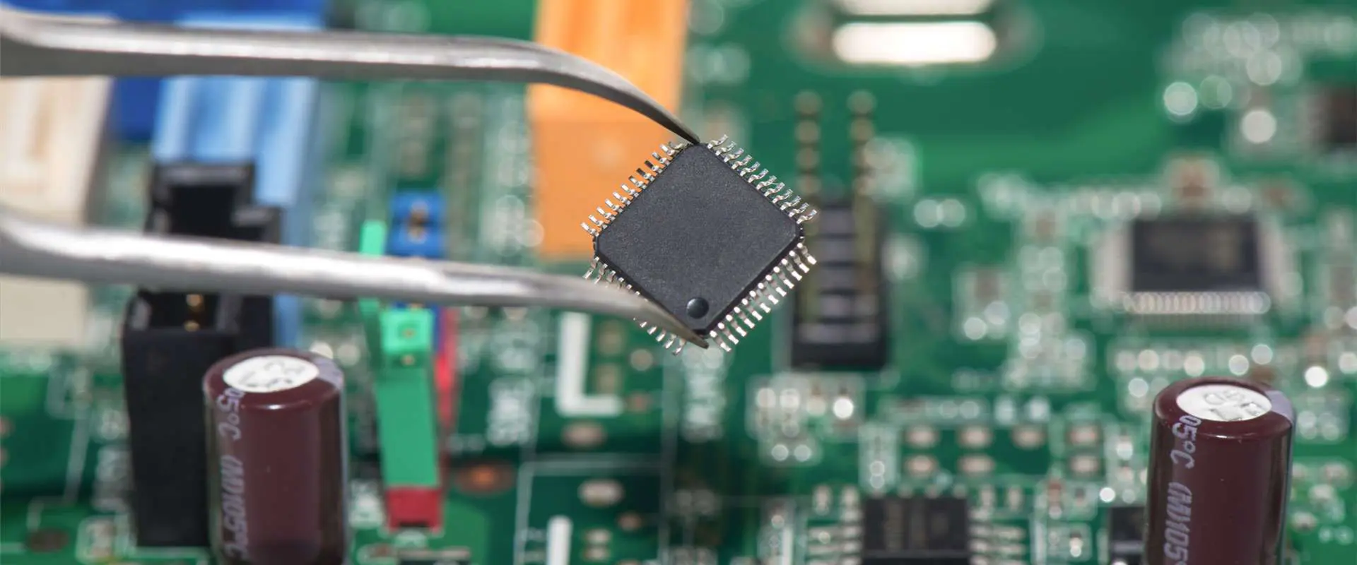
Do you know how different gadgets switch between different modes when you press certain buttons? Or how you trigger certain functionalities when you touch the screen of a touch-screen device? Well, the magic behind these functionalities is known as PCBA or Print Circuit Board Assembly. Modern-day gadgets are not just simple appliances with wires and a few functionalities. Modern-day gadgets have become helpers due to their outstanding capabilities and their compactness. PCBA brings together various electronic components onto a pretty small area; hence they achieve compactness. The parts, though minute, match or even outdo similar but larger traditional components. They are thus more productive too. But how does PCBA achieve this? Well, it achieves this through a process known as an SMT process. But what does the SMT process entail? And what exactly is SMT?
SMT stands for surface mount tech. It is a new method that manufacturers utilize to mount electronic components on print circuit boards.
Basically, SMT involves the soldering of SMCs (surface mount components) onto PCBs via reflow soldering.
SMT Process
Material Examination and Preparation
In this step, the manufacturer prepares the PCB and SMC and checks for flaws in both of them. The Print Circuit Board mostly has flat gold plated copper, silver, or tiny-lead pads which have no holes. These pads go by the name solder pads and are crucial in the SMT Process.
Stencil Preparation
The Stencil provides a fixed solder paste printing position. The design of the Stencil perfectly matches the solder pad’s positions on the PCB. In doing so, it makes mounting pretty easy to accomplish.
Solder Paste Printing
The Solder Paste in these steps is a mixture of:
Tin
Flux
The solder paste attaches surface mount components onto solder pads according to specifications. Then, a stencil utilizing a squeegee at an angle of 450 to 600 applies the solder paste onto the PCB board.
SMC Placement
Now it is time to mount electrical components onto the PCB. Manufacturers utilize a pick and place machine for this process. The machine accurately mounts SMCs onto the board accordingly. Once the mounting process is over, the PCB moves on to the reflow soldering process.
Soldering oven – When the surface mounting process is over, the PCB enters a reflow soldering oven.
Preheat zone – The very first zone inside the reflow oven is the preheat zone. In this zone, the board’s temperature plus that of all the components attached to it raises gradually and simultaneously. The rate of temperature ramp-up in this zone is about 10C to 20C per second up until it hits 1400C to 1600C.
The soak zone – The PCB remains in this zone for about 90 seconds on temperatures ranging between 1400C to 1600C
Reflow zone – The PCB then goes inside a section that has a temperature ramp-up of 10C to 20C per second. The temperature gradually goes up till it hits a temperature range of 2100C to 2300C. Once the reflow zone hits this high temperatures, the tin found inside soldering pastes starts to melt. The molten solder binds the SMC’s leads onto the PCB’s pads. The molten solder’s surface tension helps keep the SMCs in place.
The cooling Zone – a zone that makes sure the solder paste freezes as it exits the heating zone. By passing through this zone, the print circuit board avoids any joint defects.
In case the PCB is double side you might have to repeat this entire process using glue or solder paste to hold the SMCs in place.
Cleaning and Inspection
The PCB cleaning process after soldering is pretty essential. Once the cleaning process is over, the operators check for flaws in the PCB. If any defect is found, then they have to repair or rework the defect before storing it.
Standard machines that come in handy during this entire process include:
The SMT assembly process plus how to efficiently upgrade it
They decrease the rejection rate and improve the pass rate
Testifying and implementing unique strategies for manufacturing purposes
Setting the process parameters
They evaluate new methods and new components
Briefly put, we can say that an SMT process engineer prepares, implements, and then monitors the entire SMT process.
Since technology advances, so does the responsibilities of SMT process engineers. However, any additional role has to align with a particular tech advancement to cope with the increasing market demand.
Some Non-academic Skills that you require to become an SMT Process Engineer
Firstly, you should have the ability to predict and define possible results that might occur due to process changes. Immediately a change occurs in the SMT process. You should have enough sensitivity to accurately predict the corresponding results. Using this predictions, manufacturers can make a timely changes to affect other processes positively.
Secondly, you should know every tool that helps execute the SMT assembly process. Competition in the electronic market as per the 21st century is pretty tough. Clients now require devices of high quality and at an affordable price. The only companies that can afford this feat at those that utilize efficient tools. Therefore, SMT process engineers should have proper knowledge of SMT process tools, how they work, and any advances of the same. SMT process engineers should greatly embrace development.
The SMT process features so many elements such as:
Component package
Technical requirements
Materials
Equipment et cetera
Hence there should be someone who can easily understand, explain and also monitor the entire process.
Companies worldwide are under constant pressure to improve on quality to match higher quality products. The competition is pretty intense, and those who lose ultimately go under. Also, when it comes to optimizing the SMT process, manufacturers highly depend upon SMT engineers. They help them produce electronic gadgets in bulk using less money, improving their profit margin.
Conclusion
The need for SMT assembly grows every day. Clients want gadgets that are:
Compact
Fast
Efficient
Cost friendly
With SMT processes, manufacturers can achieve this feat. However, due to technological advancements, this needs gradually change. For example, clients now want a faster component with better battery life. Hence we have SMT engineers. These engineers help manufacturers cope with the current market. They help them produce quality each time using minimum resources. Therefore the next time you see a company launch a device update that might be thanks to a certain SMT process engineer.
Just like energy, we tend to hear the term power a lot. That is because, in our everyday life, power has a lot of meanings. However, when you isolate power into physics alone, you get one specific meaning, and that is: Power is the measurement of the rate at which we execute work (or, in a similar case, the rate at which energy is efficiently transferred from one location/place to another).
The ability to measure power accurately was one breakthrough that helped early engineers invent steam engines which brought about the industrial revolution. However, up until today, it remains essential to learn and understand the uses of power and how to utilize it in the most efficient way possible.
The Power Formula
Watts (W) is the standard unit used in the measurement of power. The unit got its name after a great Scottish industrialist and inventor known as James Watt; you can guess why the name watt. In the industrial era, we use the term “watts” in many objects, from machinery to home appliances and gadgets. You have most probably come across this term more than once, no doubt about it. For example, power outputs of appliances such as bulbs are generally advertised in watts hence chances of hearing this term goes further up.
By definition:
One watt = one joule of work done per second.
Hence, to measure power denoted as P in watts, we have to find energy change (ΔE) after execution of a certain job, then find the time taken to execute the job (Δt). With these two values in our possession, we can now calculate power using the following power formula:
P = ΔE/Δt
Have you ever heard of the term horsepower? Well, this term is also used as a unit for power, not as a substitute for watts, do not get mixed up on that. Horsepower is usually abbreviated as hp and gains its origin from the 17th century. In that time and age, horsepower referred to, you guessed it right, the power of an actual horse. Well, not typically the power of a horse as per their body, but the power of a horse when in use to turn a capstan. Since then, the metric horsepower (hp) has been in use as a measure for power.
We can define horsepower as the amount of power required to lift seventy-five kilograms of mass across a distance of one meter in one second. People from the 17th century were able to measure the power of a horse efficiently using this method. But how many watts are in one horsepower?
Well, using our standard power formula, P = ΔE/Δt, we can easily get how much watts are in one horsepower as follows:
Since we know that when lifting against gravity, gravitational force affects the mass whereby it gains gravitational potential energy (Ep = m * g *h), hence, putting this into numbers, we get:
(75 kg * 9.807m/s2 * 1m)/ 1s = 735.5 watts
How can we Measure Power that is Varying?
In so many occasions whereby energy is being utilized, the rate of utilization varies over time. It might start at a high rate, go down, streamline for a while and then go up again. Take, for instance, the power consumption of a house (or home): During the day, most houses have minimal power consumption because all the lights are mostly off and grown-ups are usually off to work, and kids are in school, so no televisions are on too. However, at night every bulb is usually turned on, and the kids are busy watching tv while grown-ups are preparing meals. You can hence see clearly that at night, power consumption goes pivoting up, while during the day, there is minimal power consumption. That is what we basically call varying power consumption.
There are at least three separate ways in which we can express power in the situation named above:
Instantaneous power (Pi)
Average power (Pavg)
Peak power (Ppk)
Electricity companies have to keep track of these three power expressions.
Instantaneous power
Refers to power measured at a specific given instant of time. Considering the power equation, P = ΔE/ Δt, instantaneous power is the measurement gotten when a change in time is pretty small, actually extremely small. If you plot a graph of power VS time (P vs. t), then the instantaneous power would be the value you read from the graph plot at any given time instance.
Average time
Refers to power measured over an extended period, i.e., when the change in time in the power equation is long. One method you can implement to calculate average time is finding the area under a power vs. time curve (which provides the total amount of work done) and dividing this value by the time taken. To get the best answer, you should solve this problem using calculus. However, you can still get an estimated answer using just geometry.
Peak power
Refers to the most significant/maximum value that the instantaneous power can take in a specific system over an extended period. Stereo systems and car engines are great examples of systems that can deliver peak power that is way higher than their power average rating. However, to avoid damage, this peak power is only maintained for a short period. Nevertheless, in the systems named above, we consider high Ppk more important to the listening and driving experience more than a high Pavg.
The power equation connects the work done with the time used to do the actual work. Since we already know that work is executed using force, and force can ultimately move objects, we can take the concept of power even further. Using the power equation, we learn a couple of things about the movement of a body over a specific amount of time. All we need to do is manipulate the equation, and the output will amaze you.
By substituting the amount of work executed by a specific force, say W = F*Δx cos x, into the power equation, we get:
P = W/ Δt being equal to P = (F* Δxcos θ)/ Δ
If, in this case, the force lies along the motion’s direction, then cos θ = 1, you can then rewrite the equation to:
P = F *v
Since we refer to the change in distance over a given period as velocity, we can write Pi = m * a * v.
Note that in the above-given equation, Pi = m * a * v, we have specified P as instantaneous; this is because the equation has both velocity and acceleration; therefore, velocity is changing over some time. All this can only make sense if we record and use velocity at a given instance. Otherwise, we shall need to implement average velocity as follows:
Pavg = m * a * ½(vfinal + Vinitial)
Using this equation, you can attain some pretty beneficial results. Take, for instance, a car with a mass of 1000 kilograms and as advertised, to the wheel, power output of up to 75 kilowatts (that is about a hundred horsepower). Furthermore, let’s say the advertiser claims that this car can gain constant acceleration over the range of 0 – 25 m/s.
Calculating time
By implementing the above information, we can easily calculate the time the car should use while in ideal condition to accelerate from 0 to 25 m/s.
Pavg = m * a * ½ v final
Since acceleration is Δv/ Δt:
Average power = m * (vfinal /t) * ½ v final
= (mv2final )/2t
You can then rearrange this to get:
t = (v2final * m)/2*Pavg
= ((25m/s)2 * 1000 kilograms)/ 2.7000 W
= 4.17s
In real life, this acceleration is practically impossible because we have to consider the work occurring in the opposite direction (the negative work). Negative work occurs when the car gradually pushes air aside to move in the forward direction.
Before we get into the dimensional formula of power, let us first go through the dimensional formula and its uses to understand the dimensional formula of power concept better.
The Dimension Formula
The dimensional formula of a physical quantity simply refers to that expression representing which base quantities have been included in the quantity and how.
We use the dimension formula to check the correctness of a formula dimensionally. It is also required in the conversion of systems from a particular unit to another. The dimensional formula is also used to explain how we express physical quantities in terms of fundamental units.
For this formula to work, there must be a multiplication-type dependency. Therefore, the derivation of formulas containing logarithmic, exponential, and trigonometric functions is impossible using this given method. Furthermore, formulas having more than a single term subtracted or added, for example (S = ut + ½ at 2), we cannot derive this by implementing the dimensional formula.
Dimensional Formula of Power
Up to this point, we based our discussion on the power equation (P = ΔE/ Δt). But now, let us switch our focus to another formula known as the dimensional formula of power.
The dimensional formula is as below:
M1 L2 T-3 whereby:
M represents mass
L represents length
T represents time
But how did we get to this absurd equation? Well, here is how:
Let’s say that Power (P) = Work x time – 1 = Joule x second -1 ……. (Step 1)
Since, Work = Force (M x a) x displacement = M1 L2 T-2L
Hence, the dimensional work formula = M1 L2 T-2…… (Step 2)
By substituting equation two into equation one, we get:
Power = Work x time – 1
Or P = [M1 L2 T-2] x [T-1] = M1 L2 T-3
We can hence conclude that the dimensional power formula is equal to:
M1 L2 T-3
Dimension simply refers to the depth, width, and height of objects or things. We refer to the amount of measurable space as dimensions.
The dimension formula simply reveals which and how many fundamental qualities are available in a physical quantity. So it is a pretty essential aspect of measurement and units.
While on the topic of power, what comes to mind first, well without even reading your mind, we can already tell that you are thinking about electricity. Well, that is because electricity is considerably connected to power; some people even refer to electricity as power. So, to ensure we do not leave any stones unturned, let us look at electricity and its formula.
Electric energy stands as one of the most crucial scientific concepts. However, it is still pretty frequently misunderstood by many. So what is electric energy? And what formulas do we use in the calculation of electric energy?
Electric Energy
To start us up on electricity, let us first look at electric energy before advancing to formulas used to solve for electric power.
Electric energy is energy we derive from the kinetic energy of charged particles or electric potential energy. Basically, we refer to this kind of energy as energy converted from electric potential energy or energy generated from the movement of electrons from one location/point to another.
Charged particles moving along or through a medium constitutes electricity or current.
Electrical Energy Formula
Every cell has two terminals, namely the negative and the positive terminal. The negative terminal contains electrons in excess, while the positive terminal is deficient in terms of electrons. Now, let us use A to represent the positive terminal; hence the electrical potential of this terminal becomes V (A). Similarly, let’s describe the negative terminal using B, whereby electrical potential becomes V (B). With this in mind, we can now define the flow of electric current as V (A) > V (B); this implies that current flows from A to B.
The potential difference between A and B is hence given by:
V = V (A) – V (B) > 0
The potential energy of charge denoted by Q at A is simply Q V (A), and at B, it’s Q V (B). Therefore, we calculate change in potential energy as:
∆Upot = Finalpot – Initialpot
= ∆Q[(V (B) – V (A)] = – ∆QV
= -I V ∆t (since I = ∆Q/ ∆t)
Taking into account the system’s kinetic energy, it could also change if the charges contained inside the conductor moved with no collision; this maintains the system’s total energy. When we convert the total energy, we get:
∆k = – Upot
Or ∆K = I V ∆ t > 0
Therefore, in the electricity field, whenever charges move freely across conductors, there is an increase in kinetic energy as they move.
When the moving charges collide, the energy gained by both of them is shared between their atoms. However, the collision also increases the atom’s vibration, which ultimately increases the amount of heat generated by the conductor. Therefore, some energy is usually dissipated in the form of heat in actual conductors.
Electricity uses two basic measurement units that are:
Watt – per second
Joules
When a single ampere of current passes/flows through a circuit for one second with the potential energy of one volt applied across it, this is what we term as one joule of energy.
Kilowatts per hour is the standard commercial unit for electrical energy, also termed the B.O.T. (Board of Trade unit).
1 kWh = 1000 x 60 x 60 watt-second
1 kWh = 36 x 105 joules or Ws
Here is something to note: when we talk about one unit, we are basically talking about one kilowatt per hour.
Examples of Electrical Energy
A car battery – a chemical reaction occurs which leads to the formation of electrons that possess the energy to travel in an electric current. The moving charges generate electrical energy that the car’s circuit uses.
Lighting – lighting is basically an electric discharge from the atmosphere.
Electric energy conversion to mechanical energy
Through different procedures and manipulations, we can convert electric energy into various forms of energy, for example:
Heat energy
Light energy
Motion et cetera
Here are some examples of electric energy to mechanical energy conversions:
Fans – fans contain motors that convert electric energy into mechanical energy
Bulbs – bulbs convert electric energy into light energy
Now that we know all about electricity, how about we take things up a notch by connecting electricity to power.
Electric power refers to the rate at which energy in an electric circuit undergoes transformation or the rate at which execution of work occurs. Basically, electric power is a measure of the amount of energy utilized over a given period.
In physics, electric power refers to the transfer rate of electrical energy by a circuit per unit of time. In this case, energy can refer to:
Potential energy
Kinetic energy
In most cases, potential energy is usually considered (potential energy refers to the energy stored because of the electric field’s or charged particle’s relative position). We measure electric power in Watts, and is denoted as P.
Symbol
P
Vector or scalar
Scalar quantity
S.I. unit
Joules, watts per second
Power formula electricity-based
P = VIWhereby, I refers to the electric currentV refers to the potential difference (volts)
Earlier on, we discussed the energy dissipated because of the heating up of conductors. In a time interval of ∆t, energy dissipated becomes:
∆W = I V ∆t
The power dissipated is actually energy dissipated per unit time, which is ultimately given by P = ∆W/ ∆t. however, we do know that the power equation is:
P = IV
With this in mind and the Ohms law (V = I.R.), we can make some manipulations to get:
P = I2R or P = V2/R
If you ever wondered why coils heat up, well, there is your answer. The power you gain via this formula is responsible for the production of heat and light.
Electricity Formulas extended
Well, electricity formulas go further and get more defined to bring to light more details on this incredible energy. Here are some of the most commonly used formulas for electricity.
Current (I)
Current refers to the flow of electric charge carriers, usually electron-deficient atoms or electrons.
We can calculate it using the following formula:
I = Q/t whereby,
Q = charge
t = time taken
We measure current in amperes (A).
Voltage (V)
Voltage refers to the pressure that comes from an electric circuit’s power source, which pushes charged electrons through a conducting loop. In doing so, it enables these charged electrons to do work such as producing heat and illuminating light.
In the early days, people referred to voltage as electromotive force or emf. That is why even in certain equations like the ohms law, we denote voltage with the symbol E.
To get the voltage of electric energy, you can employ the following formula:
V = W/Q
Or
V = E/Q
W = work done
E = Energy
Units of measurement for voltage is volts (V)
Resistance (R)
Resistance refers to the measure of current flow opposition in a given electric circuit. All materials, at some point, resist the flow of a current. Hence, we separate materials into two broad categories according to their resistance, namely:
Conductors – These types of materials offer minimal resistance. They hence transfer electric currents pretty well. Examples of conductors include aluminum, gold, copper, and solver.
Insulators – these materials present pretty high resistance; they hence restrict current flow. Examples of insulators include plastic, wood, glass, paper, rubber.
To gain resistance of a certain object employ you can use the following formula:
R = ρI /A where,
ρ = resistivity
A = Area
I = length
Or
R = V/I
The units of measurement for Resistance are in ohms (Ω).
Conductivity
Electric conductivity is the measure of how electric current navigates within a substance. Also, high conductivity within certain materials equals to high current density for a given applied Ppot (potential difference).
To get the conductivity of a material, you can employ the following formula:
Sigma = 1/ ρ
The unit of measure for conductivity is Siemens per meter or S/m.
We implement these electricity formulas to calculate unknown electrical parameters from a known electric circuit. Each formula is unique and provides essential information.
Conclusion
Power is a term that we basically hear almost every single day. If you work in an electrical or electronics-based company, then it is a term that you most probably use every single day. Over time, people tried to explore electricity, leaving a trail of formulas that helped us know more about power. We have discussed the main formulas for power plus other branches of the main formulas that come with it. Along with power, we have discussed the very crucial scientific concept known as electricity.
Based on modernization, electricity has become one of the most used resources in the world. Scientists and researchers have also dawned upon this concept whereby they have also left a trail of formulas, each unique but intertwined they produce great information about electricity. The best thing about power and electricity is that, they only get better, hence we hope that this article has given you a great boost in this incredible topics and left you anxious to learn more.