Why You Need PCB Assembly Quotes for Your PCB Projects

Instant PCB Quote

After creating a PCB design, you need to get a manufacturer that transforms the design into a finished board. You need a PCB quote before you begin the PCB fabrication process. Getting a quote from a contract manufacturer for PCB assembly is of great importance. This is because a quote offers necessary details about the time and cost requirements of a project.

A PCB manufacturer can only produce an accurate board only when all necessary information is provided. Also, PCB quotes offer details of what you will be expecting in a finished product. Your CM works according to the information provided in the quote. Letโ€™s shed more light on what a PCB assembly quote is all about.

What is a PCB Assembly Quote?

A PCB quotation is an estimate of the cost, time, and capabilities of a manufacturer in fabricating a physical circuit board. Also, a quote isnโ€™t only ideal for the assembly process. You can get a quote for PCB design or manufacturing. This document provides a broad estimate of the capabilities of the PCB manufacturer to turn the design into a physical PCB.

A PCB quote doesnโ€™t just state the cost for the required number of PCBs, it offers an idea about the time required to complete fabrication. Also, the manufacturing process becomes easier when the quotes are accurate. It is important to include all necessary information in the PCB quote. Also, the contract manufacturer will contact the designer if there is any missing information.

In addition, the information provided in a quote is very paramount to the success of a board assembly. A manufacturer will achieve a successful PCBA if all necessary information is provided. Also, the accuracy of this information is very vital.

You can get a PCB online quotation form from a manufacturerโ€™s website.

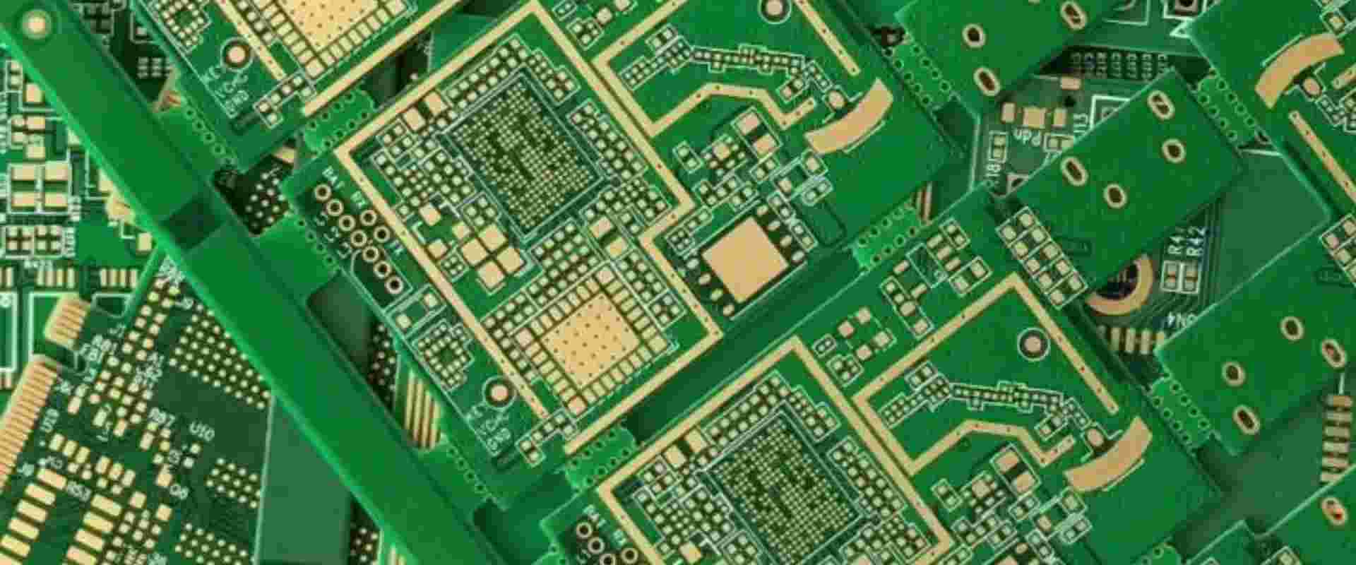
Printed circuit boards assembly quote will include vital details like:

  • Number of holes
  • Type of material
  • Number of board layers
  • Board type
  • Annular ring requirements
  • Board dimension
  • Minimum trace width
  • Outer layer copper finish
  • Minimum space between trace

What are the Documents Needed to Quote a PCB Assembly?

There are four main documents you need to quote a circuit board assembly. The information provided in these documents depends on the technologies of a company.

Bare board print

This is a vital document you need when quoting a PCBA. Bare board print is also known as a fabrication drawing. It offers essential details required to fabricate a bare circuit board. These details include number of holes, board thickness, outer dimensions, and more. Also, it offers more detailed information on what to include in the bare-board print.

Furthermore, you will need to include both the revision and component number in a bare-board print. Also, you will have to design files known as Gerber file. You will need to upload gerber file and fill the necessary details. However, ensure you supply the design files in a format. A data interchange format like ODB++.

Bill of material

The bill of material is a crucial document you need for PCB assembly quote. Also, BOM governs the components. Every line item on this document should feature a description, internal part number, and a reference designator. Also, the BOM will include the authorized vendor list. Excel is the most popular format for this document.

Assembly print

This is the blueprint of the manufacturer. The assembly print reveals information about the location of parts.  Also, it shows special markings for the printed circuit board. The assembly print should consist of the revision and assembly part number. Also, it is often available in a PDF format.

Approved vendor list

This document offers the part number of the manufacturer associated with the internal part number. Sometimes, there are multiple approved manufacturers for every IPN.

Missing Information when Requesting a PCB Quote

Paying details to information is very important when requesting a PCB quotation form. Some designers are very careful when providing basic details. This is because these details will contribute to the success of your circuit board assembly. However, some may miss necessary information. For instance, secondary details are crucial for calculating the time and cost estimate. Hence, the designer should submit them while requesting a quote.

Stack-up details

These details comprise the thickness of every layer, number of layers, and the thickness of the stack-up. Therefore, they are all crucial for creating a PCB stack-up. Also, missing this information in an exact quotation can lead to failure in PCBA.

Solder mask details

Solder mask details are crucial to share with a contract manufacturer. Also, these details comprise solder mask type, finish, color, and sides.

Impedance details

The requirements for impedance control of a PCB determine the choice of various parameters. Therefore, this information can delay the quote if it is not provided.

Cut-out

Any hole in a PCB not created by mechanical drilling is a cut-out.  Also, the positions and dimensions of the cut-out are part of the details needed for a quote.

Silkscreen

Silkscreen is information you might miss in a PCB quote. There are questions regarding where you want to apply silkscreen. Also, you need to know the color of the silkscreen you need to use.

Surface finish

The surface finish options used for a PCB impacts its functionality. Surface finish type like electroless nickel immersion gold plating and hot air solder leveling are commonly used. Therefore, it is important to provide details about the surface finish you intend to use.

What is PCB Assembly Process?

The PCB assembly process involves the mounting of electronic components on printed circuit boards.  Also, it is different from circuit board manufacturing. This process involves bringing all other components and installing them on a bare PCB.

In addition, there are several technologies used in circuit board assembly process. This includes surface mount technology (SMT) and through hole technology (THT). SMT involves the use of automated machine to place other components on a board. THT assembly involves the placement of THT components with bare hands.

There are several steps involved in PCB assembly process. The first step is the application of solder paste. Also, SMT process requires the application of solder paste. THT doesnโ€™t require this step. Furthermore, the placement of component is the next step. For THT assembly, manufacturers place components with their hands using a pair of tweezers.

The SMT process requires the use of robotic systems to place components. Also, this assembly process requires reflow soldering. Reflow soldering involves moving the PCB and its components through an oven. Also, this oven heats the solder. Thus, ensuring the connections are properly formed.

However, THT doesnโ€™t require reflow soldering. THT requires manual or wave soldering. After the soldering process, the final step is inspection. Also, the manufacturer needs to inspect other components and parts of the PCB. You can test your circuit board using the X ray test.

Factors that Affect PCB Assembly Cost

There are several factors that determine PCB assembly cost. The type of technology, the cost of material, and more are factors that influence PCB assembly cost. Also, the cost charge by a PCB assembly service differs.

Type of mounting technology

The type assembly process you opt for will determine the cost of your PCB assembly. SMT is commonly used in circuit board assembly. However, through hole technology is still in use in todayโ€™s world. Through hole parts require through hole components. Surface mount technology is a faster process for printed circuit board assembly. It using automated machine to mount SMD parts and components.

Lead time

Lead time affects PCB assembly cost. If you request the completion of your project within a short time, you will likely pay more. Shorter lead time contributes to higher PCB assembly cost.

Shipping costs

Shipping cost contributes to the cost of PCB assembly. Some PCB assembly services charge extra cost for shipping. Also, you will need to pay for shipping cost if you order large PCB quantity.

Number of layers

The number of layers will impact the cost of assembly. For instance, it costs more to produce multilayer PCBs that single PCB Qty. Also, PCB manufacturing cost will increase as the number of layers increase. This is because the lamination process involves more production step. A single board doesnโ€™t require much cost and time to fabricate.

Surface finish

The type of surface finish you choose will impact PCB assembly cost. Some surface finish options are more expensive. Also, immersion gold is a good surface finish to opt for. Also, immersion gold boasts of longer shelf life and higher grades.

Factors like impedance control, aspect ratio, PCB thickness, size of hole, and PCB size contribute to PCB assembly cost.

Conclusion

PCB assembly quote is crucial for the successful fabrication of a PCB. Also, the information provided in a PCB quote aids PCB manufacturing process. There are several PCB assembly services that offer free online quotes. However, it is important to choose a reliable PCB assembly service.

RayMing offers customer supply parts combo. Also, we offer online PCB assembly quote to our customers. Our PCBs have Ul marking and other certifications.

What are the Different Ways on How to Check Circuit Board?

Shengyi S1000h PCB

Circuit boards are major components present in virtually all electrical instrument and electronics. It has completely effected a change in the world for life. However, working with a faulty circuit board is common, even if it is not used for any technical requirement. At one point in time, every engineer has experienced a bad scenario, in which they survived.

Therefore, in order to use your instruments properly, it is very important to learn how to check your circuit board for any fault. Circuit boards are made up of many different components; this is why the board diameter may have some defects.

The common faults on circuit boards include fluid leakage, burnt circuit components, soldering issues, power related problems, and connection shorts present in PCBs.

Though the list seems long, you can check these faults quickly using a multimeter. Therefore, we will be discussing the methods when making use of a digital multimeter to check the PCB for any electrical fault. Letโ€™s consider various methods on how to test a circuit board.

Testing for Faults in Circuit Boards

Below are some vital steps that you can use as a tester for your circuit boards

  • Finding short circuits in PCBs
  • Testing for short circuits on electronic boards
  • Finding faulty components on a printed circuit board

Finding short circuits in PCBs or Faults in Circuit Boards

The multimeter is known as dependable equipment that helps in checking shorts and other electronic faults present in almost every electrical device. Making use of a multimeter circuit board, it is possible to easily inspect it for current, capacitance, input voltage, resistance, AC & DC voltage, fuse shorts, etc.

Due to the fact that it performs many circuit board testing jobs all at once, this tool is usually regarded as the combination of the voltmeter, ammeter, and multimeter.

Before using multimeter probes as a method for finding electronic faults, it is important that you go through other inspection methods. Letโ€™s consider them.

Visual Inspection

Assume you have passed the stage of breadboard design and a circuit breaker is absent, then the first step that you should take when locating the short circuits present on the PCB is looking carefully at the whole PCB surface.

Furthermore, if there is one available, make use of a microscope of low magnification or a magnifying glass all through the examination to test a circuit board.

Beginning with the power supply, search for tin whiskers present between the solder joints or pads. When you notice any blobs or cracks of solder, it should get your attention. Check the entire vias, if unplated vias is what you specified, then ensure the same holds for the circuit board. Vias that are poorly plated can help in creating short integrated circuits in-between the layers, with everything now tied to VCC, ground, or both.

When the short becomes very bad and leads to components reaching the critical temperatures, then you will see some burned spots present on the circuit board.

In-depth Physical Inspection

An in-depth physical inspection will also give you some practical and useful insights into a malfunctioning circuit board. This is also useful in identifying the faulty components, that normally, you wouldnโ€™t have been able to identify it via visual inspection alone. To get better results, you can make use of an oscilloscope.

Infrared Imaging

Making use of infrared camera will assist you in locating areas where there is large heat generation. Furthermore, if you arenโ€™t seeing hot spots away from the active components, then there is a chance that you have circuit board short circuits, even when this short is between the internal layers.

Usually, the short has higher resistance compared to the solder joint or normal trace. This is because it doesnโ€™t enjoy the benefit of getting optimized in the design. This resistance, coupled with high current that happens naturally as a result of the direct electrical connection that happens between the power and ground, this means that the conductor present in PCB short circuits will end up heating up.

Begin with the lowest possible current. Ideally, you will see this short before the short does more damage.

Testing for short circuits on Electronic Boards

Asides visual inspection, there are other ways by which you can find the major causes of a PCB short circuit.

Circuit Board Testing Making use of a Digital Multimeter

To test a circuit board for short circuits, there is a need for you to check the known resistance present between the different circuit points. However, if your visual inspection fails to reveal clues concerning the cause or location of a short circuit, then get a multimeter and then try tracking down the PCBโ€™s location.

This multimeter approach usually gets different mixed feelings online especially in majority of electronics forums. However, the tracing of the test points of the short circuit can go a long way in revealing the problem.

The multimeter to use here must have milliohm sensitivity. Furthermore, it would be great if it can alert you immediately you start probing shorts.  For example, measuring the resistance present between the neighboring pads or traces on a printed circuit board, you have to measure a high resistance.

Finding Ground on Circuit Boards

One important aspect here are short that involves a grounded plane or grounded via. Multilayer PCBs having interior ground planes will have return paths. This offers the best location to inspect and check all the other pads and vias on the boardโ€™s surface layer. Set a probe on the ground connection, and then touch the other probes all through the boardโ€™s other conductors.

Another thing is that you will also find this ground connection on other board locations. This means that youโ€™ll read an extremely small resistance when each prove is touched to two grounded vias that are different. Be very attentive to the layout when doing this, because you wouldnโ€™t want to make any error for a ground connection.

Shorted Components

When you are checking for shorted or faulty components, this means that you are making use of the multimeter in measuring the resistance. For cases whereby the visual inspection doesnโ€™t reveal excess metallic flakes or solder between the pads, then the forming of the short may have been done in the internal layers between the two pins/pads on a component.

Furthermore, shorts can also occur as a result of poor fabrication; one reason why printed circuit boards have to undergo design rule checks and DFM. Vias and pads placed near each other could short unintentionally or bridge during fabrication

For this case, you will have to measure that resistance present between the pins present on a connector or an IC. Also, pins close together are usually prone to shorts. However, shorts can still form in other locations. Check to ensure that there is a low resistance present between the pins/pads with themselves and to the ground connection.

Narrow the Location Down

Once you feel youโ€™ve located shorts between the two conductors or in-between the ground and some conductor, then you should narrow the location down by looking into the nearby conductors.

Finding Faulty Components on a Printed Circuit Board

Faulty components of components installed incorrectly could cause some problems in the board. These components could either be a counterfeit or is faulty. This creates shorts and on appearance of one.

Bad Components

It is possible for some components to suddenly gob bad. An example of this is the electrolytic capacitor. If there is any component you suspect, check it first. Now, if you are not sure you can do a Google search for the component you suspect has failed. Also, try to know if the issue is a common one.

For cases, whereby you measure an extremely low resistance present between the two pins/pads, you may end up having a short circuit as a resuly of the component that has burned out. This sign clearly indicates that the capacitor is bad. Also, capacitors bulge when they are bad or one the voltage applies passes the required amount.  

What you should do with a Faulty Circuit Board?

Using a faulty circuit board or faulty pcb could be hazardous for different electronics devices. Therefore, you may have to either replace this damaged or faulty circuit board or repair. This is mainly to prevent hazards from these damaged parts according to the EPA.

Therefore, it is highly recommended that you work with a professional electrician to assist you wit replacing the copper traces or the circuit with shorts. This ensures that the unit functions properly.

Conclusion

Any printed circuit board is usually manufactured in smaller copper traces. Also precision is used during the connection. Therefore, even a very slight defect can ruin the entire device. This is one reason why for the safety of the user as well as ensuring that the electrical devices performs for lone, you must learn how best to check these integrated circuits for faults. If you successfully identify the malfunctioning, you may either resolve it yourself quickly or ask an expert to help you out.

The Significance of a Footprint in PCB Design

Footprint in PCB

Generally, a footprint could reveal a lot of information about something. In this term, footprints serve as the result of something that arrived and left a pattern. Footprint is often a term of concern for printed circuit board designers. Footprints in PCB design refers to a pattern of a component that will be soldered there.

It could be a surface mount capacitor or a through-hole connector. Every part of a printed circuit board that requires soldering must have a footprint. Sometimes referred to as landing patterns, footprints are necessary in PCB production. Therefore, it is important to design land patterns to exact standards.

Engineers require footprint for manufacturing process. Your component footprints need to adhere to some standards just like the PCB design. Creating component footprints is a valuable skill.

What is a PCB Footprint?

A PCB footprint is an arrangement of through holes or pads used to electrically connect and physically attach a component to a board. A footprint can be also known as a land pattern. The footprint on a printed circuit board must match leads arrangement on a component.

Component manufacturers usually produce several pin-compatible products. This enables the systems integrators to transform the specific component in use without changing the PCB footprint. Many component manufacturers design footprints for their components. Land patterns look like the physical dimensions of the component. This land pattern provides an idea about the placement of component and location of traces.

Also, designers use vias and traces to interconnect land patterns on the PCB. Regardless of the component type, footprint is important. Whether it is ball grid array, SMT, or THT, a land pattern is crucial for PCB assembly. PCB footprints reveal where you need to place components in a PCB layout. Therefore, they are part of the production files sent to a manufacturer once production begins.

Accuracy is important when designing a printed circuit board footprint. An incorrect footprint will make the production process a mess. Component designators are usually encoded in your component model and this will appear on the layout when you place a land pattern.  A component footprint comprises several parts which include silkscreen, , and more.

What does a PCB Footprint Comprise?

A printed circuit board footprint or land pattern comprises the following elements:

Courtyard and outline

This is a keep out area or boundary in your land pattern. Thus, you canโ€™t place other components within the PCB footprint courtyard.

Mechanicals

There are some components featuring mechanical elements. These elements may extend above a component and cause a collision with other components. An example is a heat sink that has no electrical connection to the printed circuit board. Also, you can define this in the mechanical layer in your circuit board layout.

Hole or pad locations

Your footprint will also include the location of a hole or pad. This reveals where to locate SMD pad or THT hole. Also, these locations are important for soldering. Therefore, you must design them accurately.

Reference designator

The reference designator is an alphanumeric code that offers a unique identifier of the component in a PCB layout and schematic.

3D model

Footprints often feature a corresponding schematics symbol. The 3D model allows you to view the boards in 3D. Also, it allows 3D clearance evaluation between components.

Pin-1 designator

This reveals the correct orientation to the assembler. Some components feature arbitrary orientation.

How to Create a PCB Footprint

Designers make use of design software to create PCB footprints. Most times, PCB footprints of some standard packages are in the PCB library of the software. The land pattern must match the actual physical size of the component. Otherwise, it wonโ€™t align well with the pads. Land patterns provide information as regards the distance between pads, reference designators, and more.

The different parts of a footprint include:

  • Manufacturer part number
  • Silkscreen
  • Component centroid
  • Connectors and special components
  • 3D model step file
  • Assembly details
  • Mounting holes/SMT pads
  • Component boundary
  • Component orientation marking and Pin 1 marking

There are guidelines for creating a PCB footprint. Also, these guidelines include how to inspect, rework, and test components.

  • Begin with exact information

Make sure you have the right specifications for your part. Also, ensure you adhere to relevant standards.

  • Create footprint from the ground up

Here you need to begin with the pad information. Ensure you have everything you need. Then, create the outline of the component at the greatest material width. After this, include reference designators, silkscreen outlines, and other features.

  • Ensure you include all necessary data

There can be problems during a PCB layout if the footprint is incomplete. For example, if CAD tools state that you need to consider the height of the part, donโ€™t ignore it.

  • Be careful of adding too much data

Donโ€™t add unnecessary information to your footprint. If you include extra data, it will be replicated. Ensure you review your footprint for accuracy.

Basics of PCB Component Footprint

A PCB component footprint should comprise pieces of information. These include silkscreen outlines, reference designators and more. The information mentioned above is invaluable and should be in your component land pattern. Also, CAD tools are important as they help you create 2D footprints in various file formats. There are important points to keep in mind when designing PCB footprints:

Look out for SMD pad/ through hole sizes and locations

Land patterns need to comprise accurately size pads around the componentโ€™s edge. Also, mounting pads should be smaller than the land pads. Include the locations of the hole for through-hole components. The mounting holes or pads on these components must have correct sizes.

Include Pin-1 indicators and polarity

Polarized capacitors and diodes have cathode and anode. Therefore, you need to indicate it in the land pattern. For quad packages and Dip, you have to include some indicators of Pin-1 in the land pattern.

Keep datasheets handy

A complete datasheet will reveal a drawing f the component with necessary information like pad location and pad sizes. For instance, power MOSFETs may include a die-attached paddle or an integrated heat sink. It is important you include these details in the component footprint. Also, this is crucial for high speed and high voltage designs.

Understand package sizes

Your component footprint features the component packageโ€™s outline. This outline has to overlap the through-holes or pads on some particular SMD components. Sometimes, these dimensions are not revealed in a datasheet since the component is in a standardized package. Some examples are BGA, PLCC, and LQFP components.

PCB Footprint Checklist

Some designers have approved PCB libraries used for creating layouts. There are cases where a client sends a library with pre-made footprints for COTS parts or proprietary components. Therefore, it is crucial to check through a PCB footprint checklist to be certain your footprints match the components.  This helps you to know if the land patterns are accurate.

Here are important things to check out for in component data before a PCB layout begins:

Dimensions

You have to check the pad pitch, pad sizes, and outline them with CAD tools. It is easy to detect an incorrect component if the dimensions donโ€™t match. This will help you to know if the wrong package was in the footprint.

MPN

Some components are available in multiple packages. Also, there is always a particular code at the MPN to identify a particular package. Check if the package in the footprint matches the package of the manufacturer according to the specified part number.

Revision and lifecycle status

Most times, designers fail to check these points. Avoid end-of-life (EOL) components or NRND. Also, ensure the component footprint matches the manufacturerโ€™s most recent revision.

Basic footprint match

You can use this to detect an incorrect footprint on a component. For instance, if some connectors and other components donโ€™t have standardized packages, you can easily spot a mismatch.

Problems Associated with PCB Footprints

It is important to follow the PCB footprint guidelines to avoid some problems. These problems can only occur when there are no guidelines in place.

Small component outlines

You canโ€™t assemble land patterns with small outlines using automated production lines. You may be able to manually assemble the parts depending on how severe the error is. However, that could take more expense and time. The manufacturer may reject the circuit board if the error is large.

Incorrect pad sizes

Very small pads can result in breakout issues for THT parts. Also, this can cause bad solder joints for surface mount design. Too large pads can occupy room for trace routing.

Incorrectly spaced pads

This is another problem associated with PCB footprints. Too close or too far through hole pads can result in component insertion problems during assembly. Also, SMT design pads too far or close from each other can result in the formation of insufficient solder.

Standards for Creating a Footprint

There are certain industry standards for PCB component footprint. Also, the quality of a footprint must meet these industry standards.

IPC-7352 (PCB Footprints)

There are certain requirements provided by the IPC-77351 for SMT designs and footprint standards. According to this standard, there must be maximum solder joint quality after placing components. In addition, the IPC-7351 standard offers instructions on how to design new land patterns and utilize existing ones.  Some of the tips include:

  • Ensure the spacing around the component footprint for rework and inspection is enough.
  • Donโ€™t ignore the recommendations of the manufacturer. Ensure you strictly adhere to the recommendations for better results.
  • Test points for functional tests are necessary
  • Use a common package type whenever it is possible. There are options to transform the existing package footprints to the necessary requirements. Also, you should create a land pattern from the beginning if the package type isnโ€™t in the library.

ANSI Y32.2-1975 (schematic symbols)

This land pattern standard states that you must arrange schematic symbols by pin number. It doesnโ€™t allow the use of a pin function to arrange symbols. There is PCB CAD software that enables you to decide if you want your schematic symbols to comply with this standard.

ISO 10303-21 (3D STEP models)

This land pattern standard focuses on STEP models utilized in 3D MCAD/ECAD software. It is a file format specification. It is easier to adhere to this industry standard if your ECAD software features a footprint generator.

Conclusion

We hope you now understand what a pcb footprint is. However, if thereโ€™s any section where you need some clarification, please contact us here.

What are the Design Guidelines for Micro Circuit Boards?

Taconic RF-35HTC PCB

The electronics world will soon implode and this will be caused by great improvements in how electronic products function or a huge size reduction. This will lead to miniaturization of PCBs. Below are some tips that will explain to you how to design and manufacture small circuit boards.

Today, reduction in size in basic printed circuit boards will assist the designer in reducing their PCB size by a quarter or by half of its initial size. With smaller vias and traces, there will be a need for new design rules, because the manufacturing of printed wiring boards is more advanced and different.

Moving to a reduced line width may catch some old fashion fabricators of printed circuit boards prototype off guard. In order to stay competitive even in the future, any PCB shop should offer about 50-micron spaces and lines or even reduced to 30.

How to Design Small Circuit Boards

For some clear reasons, fine lines of about 30 microns can never make use of the usual one-ounce copper layer. As the line width is reduced the thickness must reduce as well. Copper traces that are thinner ought not to pose an issue unless you need high current for your design. In this case, you can use a wider specific trace to help handle this higher current.

Furthermore, a line of 30-micron is reliable and tough. However, it doesnโ€™t have the strength to take much physical abuse which you can nearly eliminate by using a solder mask.

These fine traces may be worrisome for many designers. However, they must know that the initial wide trace of 200-micron they begin with will drop to about 25 ro 13-micron gold or aluminum round wire. This wire helps in connecting the chip carrier to the die.

There have been new methods to adhere copper to the surface of the circuit board, and are useful in improving the general adhesion of the micro trace into the surface.

For small vias, a physical limit regarding the size exists. Below 2 mils or 50 microns, that solution wonโ€™t plate that hole wall properly. This results in a poor quality via. Furthermore, the laminateโ€™s thickness controls the viaโ€™s minimum diameter.

The microvia as a whole isnโ€™t bad. It may be smaller compared to the traces, however, sweeteners can be added to the pot since the microviaโ€™s annular ring can be smaller.

Making use of new technology for your small printed circuit boards rather than the usual circuit boards technology will lead to significant savings in real estate.

What are the Design Guidelines for a Micro Printed Circuit Board?

Below are the design guidelines for a micro circuit board.

Microvias

When making use of HDI technology, copper layers are added to the top of the multilayer board or as a HDI multilayer. Microvias are useful in connecting between these thin layers. You can drill the through-holes 5.9 mils in and a diameter with a thickness of 60 mils or you can use laser drilled hole with a diameter of about 2 to 3 mils thick.

Hole Sizes

Note that all the elements of a traditional design for a PCB have to be adjusted in order to fit the microโ€™s smaller size. This could become a challenge for layout engineers of PCB that know much about the traditional design of pcbs. One very common error here is including over-sized holes. If the design has too large holes, which usually happens, this leads to non-functioning or suboptimal micro PCBs.

Copper Thickness

The usual pattern plating is useful in manufacturing micro circuits. This means that the trace doesnโ€™t need to leave the circuit. Pattern plating helps in connecting the whole circuit. Wire bonding plating on the other hand is electrical or electroless.

Electrical Testing

A rigid probe or flying probeโ€™s lower limit is at 2 to 3 mil pitch. Over time, we expect that this drops as smaller landing pads are necessary. If the micro printed circuit boards feature smaller points like edge strip connectors, then it is advisable that the lines are extended off the circuit.

Reliability

Majority of normal laminates for printed circuits are useful for microcircuits or HDI. However, they all have limitations. You can manufacture micro double-sided or single circuits out of strong and rigid FR4 laminates. However, they must be thin to permit micro through-holes.

Security Marking

You can image small bar codes into solder mask to identify PCBs positively. Note that bar codes may be extremely small that they are invisible to the eyes.

Know the Capabilities of the Manufacturer

This is a very important step when working on micro PCB designs regardless of the microelectronic type of specific application you wish to develop.

Note that this tip is very relevant whenever you want to start anything related to PCB design. However, knowing the manufacturerโ€™s services and capability is very important for your micro PCB. This is very important for companies that have never engaged in designs of micro PCB or teamed with a specific firm involved in PCB fabrication.

The reason is because the capabilities of the fabrication of micro pcbs vary with respect to the PCB manufacturer. The fact is that micro PCBs are still new and are complex so a good number of PCB manufacturers will provide limited or no support or microelectronic capabilities. Therefore, you will need to be sure that the manufacturer has what it takes to meet all your requirements.

Circuit Boards Necessary for Small Applications

Your size of circuit board depends on the design. Creating the layout of the integrated circuits is necessary, and you can make use of a computer aided design software. With this, you will be able to reduce your circuit board size easily. The spaces present between two electrical conducting paths are 0.006โ€ or even smaller.

Furthermore, the dimension of a printed circuit board has to do with the circuitry and enclosure which houses the printed circuit board. Also, it determines the fixed components and heat sinks of the circuit board. Using the software, it becomes easy to reduce the circuit board size. It is advisable to ask the manufacturer to reveal the smallest possible size of circuit board they have the ability to make.

In addition, the circuit board size has to do with the space available for the enclosure. If the gadget you are designing is tiny, then you have to make use of small circuit boards. However, note that when creating a design for your small PCB, it will also use small electronic components. This could mean that you have to solder them using a fine tip soldering iron as well as close-up glasses or microscope, most especially when the clearances of these holes are tight.

Tips to Create the Smallest PCB Possible

When you are designing a printed circuit, there are some factors you should consider like text size, minimum width for the silkscreen, minimum width for the trace, minimum clearance for the solder mask, solder paste/minimum vias/pads/trace space, as well as the finish and drilling hole. Note that these factors aid the determination of the minimum circuit board size.

Also, make sure you consider the buried and blind vias carefully at all times. This is because they have a great impact on the design and they can engineer the PCB to become very small. Vias help in connecting the traces between the board layers, while traditional options decrease the routing space available on the board.

To maximize the routing space and to avoid any large size for your board, we advise that you search for alternatives. Blind vias help in connecting internal and external layers with reduced spacing. Furthermore, buried vias can help in connecting multiple internal layers; however, they donโ€™t reach out to external layers. This then limits the overall requirement for the space and will present you with a product that is more stable.

Also, check out the spacing present between these components. When you bring them closely together, there might be no room for trace routing. When the component has more pins, then it will surely require more space. With proper spacing, soldering the components onto the circuit board becomes easier.

In addition, components have to stick to the usual pin numbering design standard. This ensures that everything is equally oriented. This also reduces the possibility of errors during soldering and inspections. With this, manufacturing concerns are limited and this also helps you to remember everything as you undergo size reduction.

Applications of Small PCB

As electronic gadgets keep experiencing continuous miniaturization, this has caused or driven printed circuit boards into becoming denser and smaller, as well as requiring more capabilities. Now, the smallest PCB size is now the norm. This is because more small PCB design manufacturers now make use of integrated circuit chips.

Smallest PCB size is useful in different applications and industries including

Conclusion

Due to technological advancements, manufacturers now lead more towards small circuit boards. RayMing PCB is an experienced manufacturer and developer of small PCBs. It also focuses on customer services and industry tolerances. We offer professional services that can adjust quickly to meet low- or high- volume demands that may be available for small PCBs.

Contact us today on how we can help you design a reliable small PCB for your needs. You can ask for our different pricing options that meet your budget.

What is PCB Board Specification?

Isola A11 PCB

The circuit board specification gives us the details regarding the type of PCB board we desire. Understanding this specification a bit more is necessary, as it helps you tell the manufacturers of printed circuit boards the PCB board type you need.

A lot of specification for printed circuit board fabrication exists. This helps in describing the PC B product. It may not be necessary to study everything, and this could be overwhelming for the beginners, especially when all you desire is just one PCB board. Here we will be presenting to you the well known specifications that are useful in PCB manufacturing or circuit board production.

What are the Typical PCB Specifications for Fabrication?

The typical specifications commonly used by a PCB manufacturer include 1.6mm, FR4, Green Mask, 1 oz copper, HASL, and White Silkscreen. Now, letโ€™s consider each of them.

FR-4

The FR-4 is called the standard material for printed circuit boards. This material is a durable one and works for the majority of applications. Furthermore, it is flame retardant. This is why it has the name FR, and with a grade of 4. It is flame and water resistant, and has good strength. This board material is very common and is useful in PCB fabrication.

Regarding PCB fabrication, other materials are available. However, we donโ€™t advise you to use any other type asides FR-4, unless the PCB design you are working with, requires you to use that specification, or will work in that situation. These materials come with their benefits and disadvantages.

Other materials that can be useful in PCB fabrication include

  • Flame retardants like FR-5, FR-4, FR-3, FR-2, FR-2, G11, and G10
  • Composite epoxy materials like CEM-5, CEM-3, and CEM-1
  • Flexible printed circuit boards for flexibility and tight spaces
  • Aluminum, metal, and ceramic for components that generate high heat
  • Roger like RO4000, RO3000, for high-frequency applications
  • Teflon such as polytetrafluoroethylene, PTFE, Polyimide

1.6mm

This is the standard board thickness or pcb thickness. It is also very common and it offers great support for typical applications.

The pcb design of the majority of through hole components is to be mounted on a PCB board of 1.6mm. You can use 1.6mm as the recommended pcb thickness unless you are advised to do otherwise. For small and dedicated designs, it may be preferable to use thinner printed boards. For cases that are extreme, you can improve signal integrity by routing the traces on your thin PCB properly.

2 Layer PCB

For a very simple circuit, just one layer PCB may be enough. For most designs, you may end up easily with 2 layer boards. Once the number of layers is more than two, the process of PCB manufacturing becomes complicated. Also, this means the required cost will also increase.

1 oz copper

This has to do with the copper layerโ€™s thickness, which is found on both the bottom and top of your 2 layer board. The copper layer etching forms the copper trace, which helps in connecting the IC chips of the electronic circuit, as well as passive and active components. Traces carrying signals donโ€™t carry too much current; this is why the thickness of the copper layer is not usually a concern.

Green Mask

This is the major thing, which makes the majority of PCB boards have a green look. The mask is a coating layer that helps to resist molten solder. You can choose any color other than green. The green color ensures that you see the printed trace easily. This helps with maintenance and troubleshooting work.

White Silkscreen

This is a white labeling that is usually printed on PCB boards. With this labeling, you will be able to identify the value, orientation, and position of the components. Also, it is commonly used in printing the model product out, as well as other information relating to manufacturing.

What are the IPC Standards for Printed Circuit Boards?

 As a PCB manufacturer, ensuring that quality is maintained all through the manufacturing process is important. This is why it requires great and careful attention throughout the phases. IPC will go a long way to adhere to the standards.

What is IPC?

IPC is known as the trade organization or association of electronics industries. This association offers protection for electronic equipment and industry standards for assembly coupled with public policy advocacy, market research, and training.

How do IPC Standards Assist All Aspects of Your Business?

At first, PCBs can look a bit different in appearance, regardless of their quality. Customers may not see this difference always; however, they are sure that your business or company puts much effort in making sure that they get PCBs meeting even the most strict and stringent quality standards.

It is very important that PCBs work reliably during the process of manufacturing and assembly and when it gets to the field. Asides these costs, faults that happen during the assembly and wire harness assemblies may eventually get built in the end product through the PCBs.

In all the market sectors, most especially those that produce products with analytic applications, failures could be very devastating. You must consider these aspects when comparing the prices of PCBs.

For a contract manufacturer to be successful, more should be done than simply focusing on the details of the applicable IPC standards. The best contract manufacturers will embrace all these standards to ensure that the building of these processes is done on a very solid foundation.

By doing so, they are set to check out the smallest manufacturing imperfections, which would have been overlooked by some just seeking to satisfy some details. Some details usually overlooked include some processes like proper handling of the PCBA, to prevent electrostatic discharge, coupled with personnel considerations and work environment.

 What is the Significance of the IPC Standards?

Working with the IPC standards, a company will improve its products and processes in many ways. Below are some leading benefits.

Improvement in the Reliability and Quality of the Product

When you adhere to IPC standards all through the manufacturing, your company will be able to improve their productโ€™s reliability and quality. When a company creates products that last longer and performs better, this will make them more profitable and competitive. They will also improve their customer satisfaction.

Improvement in Communication

When companies adhere to IPC standards, it improves communication both externally and internally by making sure that everyone makes use of this same terminology as well as agree on expectations.

Furthermore, internally, the employees that speak similar languages will be able to collaborate and make the necessary changes to ensure improvements. These standards also help in improving the communication with regulators, supplier vendors, customers, and others.

New Opportunities and Improved Reputation

When you adhere to standards recognized internationally such as IPC standards, that company gets instant credibility. Once anyone sees that you work with the IPC standards, they will be sure that you are focused on delivering quality even if they donโ€™t know anything about your company or business.

 With IPC standards, your productโ€™s quality will be enhanced and your reputation will be improved. Ultimately, these standards will also help you attract customers, create new opportunities, and also make you very competitive.

Reduction in costs

Improvements resulting from making use of the IPC standard go a long way in reducing costs. Minimizing miscommunications and improving quality reduces the possibility of reworks and delays.

Working with the IPC standard, companies will also be able to reduce the use of resources and increase their efficiency.

Terminology for IPC Standards

In order to assist users in understanding and working with the industry standards, IPC has provided some definition of the terms it utilizes. Furthermore, this terminology also ensures that communication is more efficient and accurate throughout the industry.

IPC separates the PCBs for electronics manufacturing to three classes. The classes indicate the PCBโ€™s quality. Class 1 has the lowest, while class 3, has the highest. Companies producing electronics using PCBs must take note of the different classes. This is because they indicate and dictate the performance and safety specifications that companies have to meet.

Class 1 โ€“ for electronic products (general)

These serve applications where the main requirement is the functioning of the finalized IPC assembly. The class has to do with the majority of consumer electronics and everyday products.

Class 2 โ€“ for dedicated electronic products (service)

This class of products must possess extended life and high reliability. Though uninterrupted service is not critical, it is preferable. The productโ€™s use environment typically will not cause any failure. Laptops, microwaves, etc. are examples of products here.

Class 3 โ€“ for electronic products (high performance)

This class must offer performance when necessary or continuous performance. You cannot have anything like equipment downtime. The equipment has to function whenever it is required or needed. This category involves critical systems like life support systems. Also class 3 PCBs are useful in machine learning, clean technology, and medical equipment.

Other Terminology

Assembly: This involves subassemblies, several parts or combinations that are joined together

Acceptance tests: These are necessary to determine if a specific product can be acceptable upon the agreement by the vendor and purchaser

Resist: This is the coating material used in protecting and masking come areas of a specific pattern during the manufacturing as well as testing, from the etchant, solder, plating, and other coatings.

 Integrated Circuit: This is the combination of circuit elements that are formed or interconnected within or on one base material in order to serve a microcircuit function

Process Indicator: This is the deviation on a specific product, which doesnโ€™t affect its function, fit, or reliability negatively, like discolored insulation, solder joint with pinhole, etc.

Flexural Strength: This is the tensile strength present in a materialโ€™s outermost fiber, which must bend.

Conclusion

We hope you understand the specification for circuit boards as well as the various standards that companies should follow. Sticking to these standards brings great benefits for your company.

How to Get the Best Instant PCB Quote

Instant PCB Quote

This time and period is the best ever to get involved in the development of electronic devices with impedance control and PCB manufacturing. There has never been a greater need for very fast PCB prototyping as well as assembly service. At all times, consumers wish to be connected to different things. We wish to have control on everything i.e. sprinkler system, thermostat, etc, using our phone or tablet.

For a good number of businesses, there is a fierce competition to get their products into the market to reach its customers faster. This is why PCB assembly service and electronics manufacturing companies have evolved just to meet these demands.

Check out for these Warning Signs When Searching for PCB Quote

For decades, companies have delivered electronic devices that have printed circuit boards. The development of the infrastructure for traditional manufacturing was meant to meet the needs and requirements of large companies having large orders, lots of waiting time, and no iteration requirements. If you are searching for a printed circuit board quote, then you must check the following warning signs.

  • You must send some documents relating to the pcb design, bill of materials, gerber file, as well as other related files via email
  • A PCB quote need back-and-forth exchanges of emails with a specific salesperson and this takes about days or weeks to be completed
  • Ensure you source all the parts by yourself
  • Make sure you email or call someone to know the progress of your project
  • They are usually situated offshore; this makes travel and communication more challenging
  • You face the risk of losing your property to black marketers
  • The vendor wonโ€™t accept the prototyping order. If accepted, you will be charged excessively
  • The vendor doesnโ€™t offer fulfillment or inventory services
  • There is a huge minimum order requirement for production or much charge for little or small runs

What is the New Approach to PCB Quote?

Contrasting the old-fashioned model, the on-demand manufacturing (cloud manufacturing) ensures that service providers offer support for creating a printed circuit board as well as impedance control electronic devices from the first idea down to delivering it to the customer.

We achieve this via a platform that uses internet-based technology that ensures designers get their instant PCB Quote within minutes, manage inventory, and track projects through their browser at any time.

With on-demand manufacturing, contract manufacturers are allowed to package lots of small orders all together thereby ensuring the combination of small batch runs and prototyping orders are combined with the larger orders.

Furthermore, this helps in reducing costs and then permits them to do without minimum order requirements that are passed to the customer.

The approach for printed circuit board assembly and manufacturing of devices does something similar for developers. You put your focus on the creation of the right product and then promote it in your market.

Upload the designs via online portals. This gets you your PCB Quote within minutes. The provider of manufacturing services will then take action bringing your vision into life. Furthermore, you will have full time access into your projectโ€™s status and donโ€™t be taken aback by the costs.

Who can Benefit from a PCB Quote?

The development of printed circuit board and manufacturing of devices are now becoming very available to everyone ready to launch a new product or have a brand new idea. Entrepreneurs are creating different ingenious ideas. Small businesses have started to introduce niche devices. Even huge organizations have given time to engineers to handle projects they are interested in asides from their research and development projects.

Purchasing Teams

You can get some benefits from on-demand manufacturing even if you donโ€™t possess a background in engineering. You can email the necessary PCB file i.e. gerber file to a reliable manufacturing company like RayMing and there youโ€™ll get a printed circuit board quote for your PCB assembly.

To ensure great success, businesses should find a way to move products with high quality to the market very quickly. You donโ€™t have to wait around to get your pcb quote. This isnโ€™t an option

Small Businesses

Growing businesses and start-ups usually donโ€™t require large orders to be able to get prices that are affordable from big manufacturers. Also, they prefer in-time deliveries and also make efforts to avoid any large inventories. With on-demand manufacturing, the needs of businesses like this are met. This happens by reducing the costs involved in runs of small quantities.

Furthermore, some providers of PCB assembly provide fulfillment and inventory services. They may also provide software that can integrate the website of the business with the platform for manufacturing. This integration helps in ensuring low costs. It also allows the employees to spend some time focusing on strategic needs for the business. Note that on-demand manufacturing is a sure way that small startups and businesses accelerate their growth.

Engineers

Engineers can work in different positions, in research and development, PCB design firms, and in small businesses. Irrespective of your role, for your PCB assembly, you can work with RayMing to get your transparent and fast PCB quote at each stage of the development as well as manufacturing.

You can also create prototypes more frequently, and iterate without having any association with old-fashioned techniques for manufacturing.

Common Features to Look For Before Requesting for an Instant PCB Quote

There are lots of options available out there, therefore, choosing the best manufacturing partner for your printed circuit board could be difficult. Many manufacturers claim to offer the best services at affordable and low prices.

When applying for online PCB Quote, you will be given a quotation form or an online quotation form, you will be allowed to choose a payment method i.e. choose PayPal payment directly. You will also be asked to upload gerber file. Most pcb companies involved in high volume manufacturing deal with only pcb related Quote, anything above pcbs, then you have to find another option.

However, how will you know if they have all the features and services you desire? Below are some of the characteristics and features to check for.

Transparent Pricing and Instant PCB Quote

Once you request a PCB quote from a partner, you must have a good experience. Search for a platform that is easy to use and which will allow you to upload your bill of materials and design documents for your instant quote.

Also, the best possible solutions ensure that the pricing scenarios are easy to run. This helps in determining the price at different quantities. In addition, it helps with calculating your capital needs and setting the prices of the product.

High Ceiling and Absence of Minimum Order Requirements

Contract manufacturers that have the ability to handle orders between 1 and 10,000 ensure that you donโ€™t spend too much money up front. This assures you that once you grow quickly, your contract manufacturer will be able to help. Donโ€™t pay for any unit or units you wonโ€™t need. Also, you donโ€™t have to worry if your partner will not be able to fill your necessary needs during quick growth.

Not Involved in Sourcing

After you have seen and accepted the PCB quote, your contract manufacturer has to take up the huge task of sourcing and buying. This Company must have strong relationships for supply and also have a position of negotiating for the best possible terms and prices.

Online Project Management and Tracking

Check out for a portal that is cloud based, which makes it very easy for you to track, as well as manage your project during the specified period. Furthermore, you should have the opportunity to make some changes, get updates, and give reports on inventory.

Onshore Manufacturing

You will find lots of onshore manufacturing out there. However, they are not the available choices anymore. Now, you may decide to work with a PCB fabrication company or service which operates in your country for a PCB quote. By this, you will avoid any delays in shipping, potential issues with intellectual property and complicated communication.

Manufacturing of Hardware Device

Though you are focused on having the best possible PCB quote, it is also a great idea to have other ideas like choosing a partner, which can manufacture completed electronic devices. Working with a service that can work with your idea right from the planning and then to the customer, this will help you to streamline production, keep costs low, and simplify the vendor management.

Fulfillment services and Inventory Management

Concerning the choice of a partner that will support you all through the lifecycle of the product, why not work with companies offering fulfillment and inventory services to get your PCB quote.

They will help you to build your printed circuit board, manufacture the device, and keep it safe in the inventory until an order comes for it and it is shipped to the customer.

Top-tier partners will also assist you in reducing the shipping cost. This is achievable by having a negotiation with the carriers and then passing on the discounts to you.

Benefits of Working with a Single Partner Approach

Reduces risk

By working with a partner that stays with you during the whole production, will reduce missed communications, ensure a successful outcome, and eliminate risk as well as shipping cost. If youโ€™ll be having one partner, it must be the best one, therefore choose wisely.

Gets to the Market Faster

When you streamline the whole process by using online tools that are easy to use, instant PCB Quote, quick prototyping, you will be able to get your product or innovation to the market faster

Helps you focus on the customers and your product

One reason why some businesses will outsource some functions regularly is because they aim at focusing on the competency and core functions. They will allow someone else to take charge of the other things.

Conclusion

Here comes the end of our article on PCB Quote. Once again, make sure you work with a company that not only offers the best Quote, but is also involved in PCB manufacturing. Any questions? Reach out to us immediately.

Why Non Recurring Engineering Cost (NRE Charge) is Important for Your PCB

NRE Charge

NRE stands for Non recurring engineering. It is a term that refers to a one-time cost to manufacture and design a new product. Also, this term can have different meanings in different industries. However, in the PCB industry, NRE refers to the setup costs for producing a recently introduced PCB assembly.

What is the NRE Charge?

This is a charge that covers the development, design, and testing of a new PCB design. Also, this charge includes the up-front costs incurred during the design and manufacturing of a new product. This charge is inevitable in any PCB manufacturing.

NRE cost will have to be budgeted and planned for in the project plan. Also, NRE will add the cost of labor, material for prototypes, testing the products, and more. This cost all includes all expenses incurred in pre-production requirements and activities. Also, it covers all the software and electronics development.

In addition NRE is a one-time cost. This means that all the processes and materials will be properly reviewed and analyzed. This is to ensure that NRE cost is as accurate as the production or unit cost.

What is the NRE Charge for?

The non recurring engineering charge is in two different categories: programming and tooling.

Programming

This is also known as โ€œsetup fee.โ€ ย It usually takes labor and time to program machines for a specific PCB. The setup fee is non-recurring. The contract manufacturer can utilize the programmed data to produce the PCBA. ย Programming costs is crucial when calculating NRE.

Tooling

The expenses incurred in getting some tools add to NRE cost. These tools include fixtures, metal, stencils, artwork, and more. They are specifically made for a particular product and for a particular customer. For instance, solder stencils are like finger prints. Also, you can only use them for a kind of circuit board. Therefore, they are only designed to fabricate one PCB. After this, you donโ€™t need new stencils to continue manufacturing the assembly.

The tooling cost is the most complicated item when it comes to circuit boards. Also, it is a major part of this cost. The tooling cost requires consistency. Some engineers make a mistake because they think the PCBs involved in the project demands for multiple layers.

How to Pay NRE Cost

There are two different ways to pay non recurring cost. These break out or amortize. When you โ€œbreak out,โ€ you have to pay for programming and tooling a lot. The amortize option involves including the NRE to the unit cost. In this way, you can NRE in increments.

For instance, a contract manufacturer may have to charge $110 as per unit cost if the unit cost is $100 for each assembly. In this case, the per-unit charge will drop to $100 after paying the NRE.

The break out option is better. This is because it is difficult for contract manufacturers to monitor amortized costs. Some manufacturers donโ€™t know when to get rid of the amortized NRE.

The NRE Process

The NRE process involves several stages which include:

System definition

This stage is important. It defines the performance and functions of the proposed product. Also, this helps to determine the specifications of a product.

Design and development

This stage involves product design. Also, there is a technology roadmap to get the final phase of the new product development.

Platform design process

This consists of elements like customerโ€™s review of the plan, project plan, and statement of works. Also, this includes designing and reviewing final specifications. Once you approve the design and specifications, the manufacturer produces and delivers to the customer.

How to Reduce NRE Costs

Some parameters have a huge impact on NRE costs. Therefore, it is important to understand how these parameters affect cost. This awareness will help you minimize NRE charges.

Order quantity

You can minimize your cost by increasing the quantity of your orders. Also, you can panelize multiple projects. For instance, you placed two orders for two different projects, with each comprising 50 boards. If you separately placed these orders, your manufacturer will charge you NRE cost for each order. However, you will only get one NRE charge if you requested panelization of two orders.

Number of layers and physical dimensions

Using a greater number of layers or creating test beds for circuit boards will increase the material used and effort expended. Therefore, you can reduce NRE cost by designing a small PCB. Also, you should only incorporate multiple layers if needed.

Repeated orders

Another way to reduce non recurring engineering cost is by placing repeated order. Some manufacturers keep the programming files and stencils used in manufacturing your PCB assembly projects. If a manufacturer already has the programming files and stencils of your PCB design, it will provide a substantial discount.

Consideration During the NRE Process

Non recurring engineering (NRE) can be internally performed within the manufacturing company. Also, you can outsource to a third party service provider. The experience and skill needed for PCB manufacturing will determine this decision. The NRE costs donโ€™t just play in the regular per-unit cost of a product. However, there are factors that impact the NRE costs. These factors include:

  • Type of technology
  • New product designโ€™s complexity
  • Packaging type
  • Required skills
  • Amount of work
  • Required special procedures

When to Use Non Recurring Engineering

You can use non recurring engineering (NRE) when:

  • A producer stops supporting a customer needs ad a product to change the product and keep using the newer model.
  • A new product differs in performance with other standard products from a manufacturer
  • When a paying customer requests for added feature or capability to a product

How to Calculate NRE Cost

It is important to know how to calculate NRE cost. Calculating this cost entails deciding how large the project is. Although this cost depends on certain assumptions, you still need to consider some things. Also, NRE is a combination of the development process the project will go through.  

You need to determine your budget before you start calculating this cost. After this, you have to consider the time frame of the project. This helps to determine the cost of other aspects of this project.  Other aspects include the amount of renting or acquiring the location of the project.  Also, when calculating this cost, donโ€™t forget to include the wages and salaries of staff and personnel.

Conclusion

Now you know what non recurring engineering cost is. Any questions? Ask us immediately. We will respond as fast as possible.

What is the Role of Via in PCB

Via in PCB

There are several parts and components that play important roles in the functionality of a circuit board. The PCB via is an example of these parts. In electronic devices, a tiny green board transmits different signals. Vias serve as the building blocks of a PCB design.

For example, a PCB is available inside a smartphone with different components and chips that perform signals for several features and commands. Every time you touch the screen, one of the signals on the board is immediately activated. Vias perform most of these signals.

In this article, we will be talking about the roles of vias in PCBs. Also, we will talk about types like blind and buried vias.

What is a Via?

A via is a metallic hole that connects to the circuitry of a circuit board. This hole carries out electrical signals between the various layers of a PCB. Also, vias are holes that go through board layers for the sole purpose of conductivity. Every hole serves as a conductive pathway through which electrical signals transmit between circuit layers.

Vias pass through several levels on a PCB. The board design will determine if the hole will pass through all the layers from top to bottom. Some vias only penetrate the top or bottom layer. Some vias go through an inner layer. Vias are a crucial part of a circuit board. Therefore, PCB designers and manufacturers need to understand their roles perfectly.

Furthermore, a blind via serves as an electrical connection between layers in a multilayer board. The use of vias for connection in this board makes it easy to minimize PCB size. Also, manufacturers make the via hole conductive by placing copper cylinders in the drilled holes. Then they fill the inner layer of the via with a non-conductive material.

To define vias, one must understand the types available. Also, blind and buried vias are very crucial. Also, blind and buried vias are widely used. This is because blind and buried vias offer great benefits. Also, blind and buried vias are widely preferred among PCB manufacturers.

What are the Types of Vias?

There are different types of vias. However, the two main categories of vias depending on their position in the board layers are buried and buried vias. Blind or buried vias are commonly found in circuit boards

Blind via

A blind via is a hole that penetrates the bottom or top layer of a PCB. However, a blind via stops before any internal layers. Also, you canโ€™t see through blind vias when you hold a PCB to the light. It is just like a hidden via.  Manufacturers drill and electroplate blind vias from the bottom or top layer to an internal layer.

Drilling in blind vias can be mechanical or laser. Also, you have to be accurate with the drilling depth of the blind via. Also, you can drill blind via on the PCB directly. However, it could be very difficult to drill a blind via. That is the major reason most PCB manufacturers try not to use blind via.

Manufacturers create holes on the required PCB layers and pile up these layers to drill blind vias and electroplate. Also, a blind via helps to connect the PCBโ€™s surface layer to the next layer.

Buried via

A buried via can connect the inner layer of a PCB. Also, it is ideal for circuit boards with dense routing. Manufacturers drill and electroplate these holes between the inner layers of the PCB. Also, buried vias help to link the circuit between the inner layers.

You can drill buried vias directly on the PCB, if it connects more than three inner layers. Therefore, the manufacturer can drill the holes only on the required PCB inner layers. Also, you canโ€™t see the buried vias  in the inner layers with the naked eye.

Other Types of Vias

There are other types of vias based on their location.

Through-hole

Through hole vias are the most obvious via type. These vias penetrate all the layers in a multilayer PCB. These holes are bigger than that of blind and buried vias. It is much easier to identify this type of via with the naked eye. When you hold a PCB with a via before the light, you will see the via. Also, the light will pierce through it.

Also, through holes vias are very easy to create. All you need to do is drill right through all the layers. Manufacturers use through hole vias for plated through holes technology.

Microvias

Vias which are under 150 microns are microvias. These vias are widely used on several high density interconnect (HDI) PCBs. Also, microvias are highly preferred because of their small hole size. The size of the hole takes less space on the circuit board. In this type of via, the layer connects to one another with copper plating.

Furthermore, it is easy to copper plate microvias. This is because they are in the shape of a cone. Aso, a  microvia is capable of passing through two adjacent layers. However, it canโ€™t go further. If a board design needs a via through several layers, you will need to stack multiple microvias accordingly.

Via-in-Pad

This is one of the most popular vias today. Via-in-Pad involves using vias on ball grid array (BGA) pads. Here, the manufacturer places the vias on the BGA pads of the circuit board. Also, this design has gained more popularity because it reduces the amount of space needed for vias.

Therefore, this via enables a PCB manufacturer to design smaller PCBs that demand for less space.

Benefits of Vias

Both buried vias and blind vias have their benefits. Also, other types of vias have their advantages. The technology of printed circuit boards will determine the type of via to use.

Signal routing

Vias help to enhance signal routing in printed circuit boards. Most printed circuit boards use blind or buried vias for denser boards. Also, microvias are ideal for much denser boards.

Power routing

Vias are widely used for ground and power nets. These vias will carry more current. Also, they are always restricted to bigger through-hole vias.

Trace density

Vias increase trace density in multiple layers boards. This is because you can run vias beneath and over each other in several directions. Vias enable different traces to connect with each other. Therefore, vias serve as vertical connection factors.

Signal transmissions

Vias help to enhance signal and power transmission between layers. For instance, blind vias can help to effectively transmit signals between layers in a board. You will need to route PCB components on a single plane if you donโ€™t want to integrate vias.

Considerations for Creating Vias

There are tips that help you create good vias for PCB design. It would be of great help if you integrate maximum via structures in a PCB design. Below are considerations to keep in mind when creating PCB vias.

Signal integrity

Vias can cause signal integrity problems if it is not well created. For example, A through hole via connecting the top two layers in an eight layer PCB will have 6 layer pcb of unnecessary metal. This unnecessary metal can result in interference. Therefore, it is crucial to detect problems like these and find solutions to them. You can back drill the via to get rid of the unused metal from the line. Photo defined areas can also affect signal integrity.

Aspect ratio

The board thickness will determine the acceptable drill size when using mechanical drills. Also, a mechanical drill has a limit to how far they can penetrate through before they are unreliable. PCB manufacturers always demand an aspect ratio of 10:1 for their drill sizes.

The aspect ratio is an important consideration in designing vias. Also, you can use microvias with an aspect ratio of 1:1 if you need a smaller hole. Smaller holes require a smaller aspect ratio.

Routing density

In cases where you are routing the dense areas of a board, ensure you donโ€™t use vias to block up the ground plane return paths. Also, this could occur under dense parts such as pin-count BGAs where hundred vias are in a small area. The outer layers and hole depth can enhance routing density.

Annular ring

The via pad size is crucial. Ensure large annular ring remains after drilling the via. Also, a sufficient annular ring will keep the via in check. Without enough annular ring, a drill breakout may compromise the via.

Design Tips for Vias

Here are PCB design tip for creating vias:

  • Make use of smaller vias particularly in HDI boards. This helps to reduce stray inductance and capacitance.
  • Use controlled depth for blind vias and buried vias.
  • Ensure you fill via-in-pads unless they are within thermal pads.
  • Ensure a minimum aspect ratio for high-speed vias to prevent signal reflections. Therefore, this offers better signal integrity and electrical performance.
  • You can use blind vias and through hole vias for some pad arrangement on a BGA.
  • Use staggered vias rather than stacked vias. This is because you will need to fill and planarize stacked vias.
  • Also, use vias in the thermal pads under QFNs to allow the flow of solder to conductive planes. Thermal vias offer secure solder joints for thermal pads. Therefore, prevent the solder from floating the package during PCB assembly.
  • Check the hole diameter and fine pitch BGA components for via-in-pad.
  • Also, check the copper foils and component leads.
  • Ensure you check the outer layer. The outer layer helps to create a good via
  • Check the blind via for any irregularities

Conclusion

Vias create pathways for the flow of thermal and electrical current between different layers in a board. Also, these vias vary in type and size. The requirement of a circuit board determines the type and size of vias to use. Also, vias help to enhance signal integrity in circuit boards.

Annular rings and multilayer lamination are important in the entire board. Also, copper pad and surface components are crucial in designing vias. Multiple vias and signal traces are widely used in PCBs. The outer layers are also important

What are the Requirements for Building a Circuit Board Prototype?

PCB prototype assembly suppliers

Testing your schematic design and prototyping it is a very significant stage during the process of PCB manufacturing. With prototype printed circuit boards, you will be able to spot any design flaw and find solutions to them.

Before sending your product to the PCB manufacturer, you have to ensure that youโ€™ve checked out all the design flaws and bugs. You definitely donโ€™t want lots of defected or faulty products attributed to your name.

Furthermore, when you prototype the pattern of your circuit board, this is another concept proof. Both is useful in showing proof of your property and demonstrating this product to your potential buyers and investors.

But, what does prototype PCB board mean? Here, we will address what prototype pcbs are, their uses as well as the build requirements they are involved with.

What is a Prototype Circuit Board?

Prototype printed circuit boards form an important step in the process of designing an electrical item. Furthermore, they utilize conductive tracks in connecting components.

Also, in contrast to the traditional circuit boards, the printed circuit boards feature lower costs of manufacturing. Due to their printed nature, process of complex wiring isnโ€™t necessary.

Furthermore, businesses offering electronic design can get some benefit from quicker turnaround time, because the process of PCB manufacturing is less labor-intensive compared to the traditional circuit boards.

Because of the absence of wiring, the PCBs are usually more reliable and safer. Furthermore, using PCBs will also prevent the wires from breaking loose or snapping.

Differences Between Solderless Breadboards and Prototype PCBs

A breadboard without solder is very useful in the development of electronics. They have been useful since the 1970s. The breadboards are made up of spring-loaded clips, which allow electrical connections. Also, the breadboards are not permanent and you can reuse it for different designs. This makes this tool very important for prototyping.

Furthermore, they are useful in testing a designโ€™s functions before you can make up the printed circuit board later. Some limitations come with breadboards. They can only function with the through hole components. However, a PCB typically makes use of surface-mount components.

Though breadboards may be used for some circuits, it could cause issues when using breadboards as a prototype due to the absence of surface mount components.

In majority of cases, the modern circuitry ought to feature prototype PCBs that are made up instead of going for breadboard prototypes.

The Make up of a Circuit Board

Circuit boards come in different types. The most known of them are the single-sided ones, that feature copper tracks that connects the components on just one of the sides of the printed circuit board. These are referred to as the one layer PCBs. You can also see multi-layered PCBs and double-sides PCBs.

Printed circuit boards are composed of several elements. These include silkscreen, solder mask, copper, and FR4.

Silkscreen

The silkscreen is the last or final layer present on the PCB. This helps in printing numbers and letters to the PCB. This helps during the PCB assembly process. The most accepted color is white; however, you can use any color.

Soldermask

The function of the solder mask is to help in insulating the copper traces. The solder mask helps in preventing solder jumpers. It also ensures that the copper doesnโ€™t come in contact with other metals.

Copper

This is laminated onto the circuit board. The process involves adhesive and heat. The copper plates utilized helps in determining of the board is a one-layer type or double-layered or two layer or multilayer.

FR4

This is also called flame retardant. It is an epoxy resin laminate that is glass-reinforced. This is the major element of a circuit board. It os the part that give the board rigidity

What is the Manufacturing Process for Printed Circuit Boards?

Two different processes exist during PCB fabrication. These are surface mount and through hole.

For surface mount, the soldering is done directly to the board. For this, you donโ€™t have to use leads. The benefit of this technology over the through hole method is that creating smaller PCBs, which have the ability to perform complicated processes is possible.

For through hole technology, it makes use of leads that are inserted into the holes on one of the sides of the circuit boards. Then, these are soldered onto the copper layer present on the other side.

Requirements for Building a PCB Prototype

There are some things you need to put in place before building circuit board prototypes. Most especially, the right documentation must be ready.

Focus more on creating easy-to-follow and readable documentation. This will make sure you have the right design. Furthermore, the documentation for your PCB manufacturing must not be an afterthought.

In addition, this PCB documentation has to have some context. Now, this is relevant when these designs are meant for proprietary or innovative technologies.

To make sure that you have the right documentation for your PCB, and ensuring that the entire process is very easy, follow the steps outlined below.

  • Make use of templates to help save time
  • Make sure you take note of all the deletions and edits that you have made when making use of copies based on the older documentation.
  • Ensure that you review and have a sign-off process. This ensures accuracy
  • Make sure that the documentation matches your completed design
  • Ensure that the part numbers are updated.

Summarizing this section, I will say that while seeking out prototype circuit boards that are professionally made, you must ensure that the information you are giving out is checked thoroughly.

When there are errors present on the page, this can lead to faults affecting the prototype. Furthermore, this can result into a testing process that is more expensive and more protracted.

Necessary Files for PCB Prototyping

The files outlines below are very important in pcb prototyping. This helps you to achieve the PCB design easily and successfully.

Asides from this, ensure that the board outline is incorporated within the drill drawing and solder mask images. These files include

How to Avoid Issues with RF & Signal Integrity When Utilizing PCB Prototype

Lots of issues may area with the design for prototype boards. This relates to signal integrity, RF and EMC considerations. There are many ways by which you can avoid these issues, which relates to trace routing. These include:

Cross Traces at 90 degrees

If the crossing of two signal tracks happen, then it must be done at right angle (90 degrees). With this, you are reducing the possible level of mutual capacitance and inductance between the signal lines.

Routing of the Traces should not be done in Parallel

When traces run in parallel via any length, it will experience a crosstalk level that is higher. For this scenario, the signals present on one of the traces will appear on another.

Factors Affecting the Overall Cost of PCB Prototype

You will find it hard to estimate what your PCB prototypes will cost until you engage the manufacturer. The price that the prototyping service will charge depends on the size, complexity, design, components, and materials. This is one reason why having a general estimate for price is difficult.

If the production batch you have is smaller, you will incur higher costs for PCB prototyping. Below are the factors that affect the cost of your printed circuit board prototypes.

Material

Some PCB laminate materials and substrate have more costs compared to the others. Obviously, the material for your PCB prototypes will be more expensive when you give high performance a priority.

Size of the board

When your prototype PCB has a larger board, then expect it to be more expensive and vice versa.

Speed

If you need your prototype pcbs to be handled faster, then expect to be spend more.

How to Ensure High Quality of PCB Prototype Services

Before the shipping of the board to you, there are some control tests that happen during the process of PCB prototyping. These include:

Aging Screening

This helps you evaluate the reliability of the PCB prototype, which may be in continuous operation for more than 100,000 hours. Furthermore, the test helps you examine the entire PCB assembly.

Functional Testing

This is to help pinpoint manufacturing issues and flaws that can affect missing or incorrect parts, reliability, and opens/shorts in nets or solder connections.

Vibration Testing

This involves the shaking or shocking of the components of PCBA to observe the way in which they can cope with the real environment.

In-Circuit Testing

This method is the moist common and robust method of checking PCB quality control. This automated testing checks for shorts and opens present in circuit boards. Also, it helps in detecting 98% of faults.

Conclusion

Here comes the end of our article on prototype PCB. We have discussed the make up, manufacturing process, as well as the requirements before creating one. Contact us today at Rayming PCB for your prototype pcbs

BGA Layout Tutorial: What are the Guidelines for BGA Routing?

BGA Layout Tutorial

As of today, the standard when packaging different advanced multifunctional devices like microprocessors and FPGAs are BGAs (Ball Grid Arrays).

You can break BGA packages down into micro and standard BGAs. With the electronics technology of today the request for input/output availability poses some challenges, even for PCB designers that are experienced.

In this article, we will be giving you some guidelines on applying BGA routing, challenges of BGA routing and strategies to help overcome the challenges with BGA PCB design.

BGA Routing Guidelines

There is a continuous increase in the demand from consumers for the smaller electronic devices having great functionality, PCB designers continue to lean towards BGAs (Ball Grid Arrays). This is why we have decided to give some BGA routing guidelines to help you out.

Making use of BGAs will allow PCB designers the use of PCB boards having greater functionality in smaller products. Normally, BGAs should be used for multilayer printed circuit boards where vias are useful in the routing of signals between the copper layers. It seems difficult for BGA routing to happen in complex designs of PCB layout.

With vias, you are sure that the process of the PCB design will have some flexibility, and the PCB assembly and PCB fabrication process will have some complexity. Just the same way there are placement restrictions, tolerance considerations, as well as the best practices for traces and design, the same holds for BGA connections making use of vias.

When you apply the best practice for BGA routing, then you can be sure that the PCB boards will not be too susceptible to challenges, which could affect functionality and manufacturability.

What are the Challenges of BGA Routing?

BGA routing creates some challenges, which you must consider while designing the printed circuit board. Of all these, the most important has to do with ensuring the reliability, manufacturability, and to optimize signal integrity of the board.

Reliability

Your boardโ€™s reliability has to do with the quality of the board construction and how your design synchronizes with the PCB manufacturerโ€™s capabilities by working with good design for manufacturability (DFM) practices.

Not pushing the limits or synchronizing the limits very far could result in a PCB board, which doesnโ€™t function according to the design or at one point in time, may fail once it is deployed for use.

Thickness of the solder mask, structure of the copper grain, coverlay thickness, and copper weight are issues with the material, which causes the failure of the board in the field.

Furthermore, trace routing, which includes via choices, could also affect the operation, thereby leading to huge costs for replacement and recalls. Applying the DFM check at Rayming PCB, which integrates these considerations on any board, which includes Ball Grid Arrays, will align the design of the PCB layout with the capabilities of the board manufacturer.

Manufacturability

Asides from determining the available signal layers (reference and signal) to help in optimizing the signal integrity, then there is a need to consider the BGA schemeโ€™s manufacturability. There are some specific guidelines and restrictions. This depends on the routing connections of the BGA externally, as well as with each other.

The via sizes, pitch angles, bga pitch spacing, hole drilling type, and available signal layers are limited by the PCB manufacturerโ€™s capabilities.

Signal Integrity

 One major issue with signal integrity has to do with impedance control. This affects reflections and transmission. The control of the impedance is made possible by matching the trace width between the return and forward lines, making use of the appropriate dielectric thickness and also installing a plane of reference in-between the signal layers.

Furthermore, installing ground or reference planes between the adjacent signal traces is effective as well in reducing crosstalk. If the route signals remain on just one surface layer, then it is important to maintain the space between the traces.

Now letโ€™s consider some Options that can Enhance multilayer PCB Manufacturability and Signal Integrity of the Board

BGA Via Options

When designing your scheme for BGA routing, the first step is to know the signal layers necessary based on the considerations of the signal integrity. Make sure to add the reference planes where required. With the design process of the quick-turn PCB, within a few days, you will have PCB layers with a thickness of 30 layers.

Furthermore, the next available step is determining the ways to route these BGA signals. There are some options available to you. However, before you settle on a particular strategy, make sure you take a look at how each of these will have an impact on the PCB design.

Now, letโ€™s quickly consider what a through hole and blind vias is.

Through Hole Via

 Through hole routing is a conventional method to use when connecting the through vias. This extends through the whole board. For through hole vias, you will get a great signal integrity and implementing it is easy. However, one drawback of this is that they need much space compared to the others.

Blind Vias

When routing from the Ball Grid Array directly, blind vias offer you an alternative in contrast to through-hole. Blind vias offer the benefit of incorporating staggered vias, stacked vias, or combining these two.

For stacked vias, this permits a design that is denser. However, for staggered vias, there is no need for precise alignment, which stacked vias require. Considering the PCB fabrication, the tolerances ensure that the staggered vias are implemented in a simple way.

In the end, you have to determine if you should make use of the dogbone routing or via-in-pad routing. Here are the tradeoffs in space and complexity that you must consider.

Dogbone Routing

For this routing type, the via is neutralized from its pad and then connected via a short trace. This creates a shape that is similar to that of a dog bone. Furthermore, dogbone routing doesnโ€™t have to be capped and filled as a process necessary for the via in pad routing, therefore pcb manufacturing it is faster and less complex in contrast to the via in pad.

Furthermore, there could be complex designs, and at times it may become unclear, which via style is appropriate. Now, this is an area where Rayming PCBโ€™s design team can assist. The BGA routing choice you make affects the integrity of the signal significantly, as well as the turnaround time for board manufacturing.

When you implement the guidelines for BGA routing, you will make sure of the manufacturability of the PCB board, as well as reduce the time for manufacturing the printed circuit board.

Via in pad Routing

You can reduce the space requirements of the through-hole vias by making use of the via in pad routing. The footprint for through hole vias is small. It also features an easy routing; however, it has a complex PCB design.

Blind vias help to better or improve signal integrity but routing it is difficult. The steps that are important for implementing the standard via in pad adds a huge time to the assembly process and manufacturing of printed circuit boards. The turnaround time for manufacturing can even double or triple.

With via in pad routing, the minimum pad sizes and via hole are utilized in saving space. As a result of the required precision, this could result in a breakout. Breakout occurs when a via extends outside the pad. This issue may be a significant one if the breakout happens where a trace is coming from. For cases like this, there may be loss of signal integrity. To avoid this, an alternative is the dogbone routing, which we have discussed earlier.

Strategies to Overcome Challenges Related to BGA PCB Design

Make sure you start the PCB Layout Using a BGA. BGAs are usually a deviceโ€™s main processor. Therefore, they may have to interface with different components present on the board. The common practice is placing the largest component of the BGA first and then utilize it in floorplanning your PCB layout.

Though, placing this component before any other thing isnโ€™t a must, neither must the location be locked when placed. However, the largest BGA partially determines the fanout strategy and layer count that will be useful when routing in the component.

Define Appropriate Exit Routes

BGAs having a greater layer count will ensure that the planning of an exit route has to do with routing traces via many rows of pins. Furthermore, some traces may have high-speed signals, thereby requiring the appropriate spacing of the traces to prevent any crosstalk.

Also, other signals may be signals with slower configuration, which can be brought close together without excessive noise or reduced risk of crosstalk.

Power and Ground

A very easy and simple way of managing power connections into the BGA is using power rails. This can either be on two or a single plane layer. Placing power & ground on the adjacent layers with a thin dielectric separation also helps in maintaining the power integrity by offering a high capacitance for the interplane

Determine the PCB Layer Stack

You can use the BGA I/O count and pinout on a BGA in determining the layers required for your PCB stackup. Immediately the designer determines the trace width, then it needs to route the lines of the controlled impedance into the BGA. With this, you will be able to know the layer thickness and required layer count required to maintain the impedance.

Conclusion

Whatever BGA routing you choose will have a significant impact on the manufacturability of the PCB design and the signal integrity. Also, note that your selection will most likely delay the turnaround time of your board. Implementing BGA routing guidelines as well as the best BGA routing scheme and practices, you can be sure of the boardโ€™s manufacturability, as well as reducing the PCBโ€™s build time.