How to Make BOM for PCB Production

HOW TO MAKE BOM

The Bill of Materials, popularly known as BOM plays a crucial role in the design and manufacturing stage of all electronic devices, starting from circuit boards. Without a detailed BOM, the project may need some revisions that make cause delays during production. Therefore, the BOM is one of the most critical aspects in PCB manufacturing.

Most times, manufacturers ask their customers to upload their BOM list whenever they submit an order. However, knowing the information a BOM should entail is crucial in designing one. Also, bill of materials should contain the necessary information. BOMs offer several benefits to both electronic manufacturers and customers. Therefore, it is important to understand what the bill of materials entails before designing one.

What is a Bill of Materials?

The bill of materials is regarded as a list of materials, components, and assemblies for product manufacturing. The information in the bill of materials is crucial for production.  Therefore, manufacturers must depend on these pieces of information to manufacture a product. The BOM must be well detailed and very accurate. The success of a production depends on the BOM.

BOMs are both crucial to customers and manufacturers. For instance, it helps a customer to express their needs when they order circuit boards. Therefore, the PCB assembler uses this information to fabricate the circuit board or electronics according to the requirement of the customer. Also, you can refer the BIOM as an ingredient list for manufacturing a product.

As regards PCB design, the bill of materials is a detailed list that comprises all the components and parts for PCB manufacturing. BOM helps to easily track progress during production. A bill of materials is critical in PCB design. Therefore, a BOM must be accurate and not allow any potential misunderstanding.

All manufacturers begin with the production process by creating a BOM. This is because the BOM provides basic information about the product. BOM is not only used in the electronics industry, it is used in other manufacturing industries.  Also, the BOM enhances production as the stages evolve.

What should a BOM Include?

bom bill of material

A bill of materials must include specific information about the manufacturing process of a product. Below are high-level information a BOM should include:

Component value

The component value refers to the specified value for particular components. For instance, the component value for capacitor is capacitance. Inductance is the component value for inductors. This information will help you to keep the value in mind. Also, it could help in getting alternative parts when sourcing for components.

Part number

You must include the part number of each part in the BOM. Therefore, each part must be assigned a part number. This will help you identify parts easily. Manufacturers may choose a non-intelligent or intelligent part numbering scheme.

BOM level

It is crucial to assign every assembly or part a number to know where it fits in. This provides an understanding of the BOM structure.

Quantity

This information is very delicate and as such must be in the BOM. The quantity column indicates the number of a particular component the manufacturer needs to order.
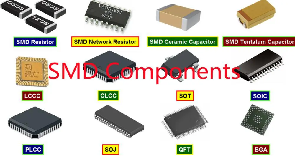
Placement method

This placement method specifies how your manufacturer should assemble your part on the board. Also, the placement method can be surface-mount, through-hole, and combination of SMD and through-hole.

Reference designators

You will have to include reference designator if you have a product that comprises printed circuit board assemblies. Also, this information can prevent confusion during the production process. Reference designators are usually labels printed in silkscreen on the printed circuit board.

Part link

The part link is just a web link that reveals more details about the part. Also, it reveals more information to you and your manufacturer.

Other information included in a BOM

Package type

This refers to the type of body that houses electronic components. Also, the package provides an idea of the shape and size of the part. Also, package can help you lay out the PCB.

Procurement type

This reveals how every part of the PCB is made or purchased. Procurement type helps to create efficiencies in procurement and manufacturing.

Alternate part number

Part stock changes over time. A part which may be in stock when you created your BOM may be unavailable by the time you begin procurement. This is when an alternate part number becomes handy. Therefore, an alternate part number offers a substitute part when your original part is unavailable. Also, it saves time spent on looking for an alternative part.

Footprint

This information reveals the number of connection points every component has on the board. In addition, including the footprint explains the arrangement of connectors like pads in SMT. Points and footprint are crucial for each BOM level and individual components.

BOM levels

BOM is a comprehensive list that contains multiple levels. Each of the BOM levels represents a sub-assembly or main assembly. Every BOM features structure marked according to the BOM levels. Therefore, the BOM level helps users to easily navigate the document and have a good understanding of the assembly.

What you should know Before Creating a Bill of Materials?

FULL PCB MANUFACTURING Quote

Before creating a bill of materials, it is important you understand certain facts. Designing a BOM can be time-consuming. However, you shouldnโ€™t skip any step. Before creating a BOM, you should consider the following questions and have answers to them.

What are you creating?

Before you decide to create a BOM, you should have started with the design phase of your project. Also, this design phase will prepare you ahead of time. It will help you know the parts, components and assemblies you will include in the BOM. Also, ensure your plan works as expected.

How should you manage the BOM?

Your bill of materials will undergo several iterations as you create it. Before you start creating a BOM, ensure you create a system for managing it. Also, ensure you use the latest version. Create identifiers for various versions. Also, you can allow a few people to edit your document. It is crucial you keep records of supporting documents like work instructions and CAD drawings.

Who will use the BOM record?

It is crucial to include several details in your BOM. In most cases, you may never have a face-to-face interaction with some people using your BOM. Therefore, your BOM have all the details they need throughout the lifecycle of the product. You should design your BOM based on the type of people who will be needing your BOM.

What information will your BOM include?

You need to know the information you will be including in your BOM list. Every BOM should comprise basic information like part name. Some items may be optional.  Also, you will need to decide if you will be including consumables like fasteners and glues. Most manufacturers second-guess whether to include consumable in their BOM.

How to Write a Bill of Materials

Writing a bill of materials is a straightforward process. However, it is crucial you follow the necessary procedures when writing one. There are softwares that help you write a BOM list without stress.

Create the document

Open the software you intend to use. After this, create a new document. Name the document and include important information at the top.

Organize the document

Create user permissions and create any levels needed. Also, you might have to include more organizational data and make changes to the data as you progress.

Fill in the columns

Here, you will have to put the names of the categories at the columnsโ€™ top. Therefore, these titles will comprise things like part number, item name, and quantity.

Fill the rows

You will need to add information to the rows based on the category of the column. Also, each component on your printed circuit board will feature a separate row. It is crucial to ensure the information is up-to-date. This will determine the success of your project.

Update information

You will need to update the details in your BOM when needed. Always remember to save all the changes you have made to the file. As you know more about the project, you will need to be more flexible in the production process.  

Tips in Creating BOM

Design your BOM based on your needs

Before creating a BOM, it is crucial to determine what you will need from it. Companies have various ways of creating BOMs. Also, the organization and information included in your BOM depends on the type of project. Therefore, you will need to customize your BOM based on the demands of your project.

Make use of a template

PCB assembler and PCB manufacturers always have BOM templates. You can get these templates on their websites or their sales departments. A template gives you an idea of what your BOM should look like. Also, it is ideal to get your template from the company you are working with. This will help to prevent problems that may arise when opening the BOM. Also, it will prevent any technical issues resulting from incompatible file types.

Ensure you include important and clear details

A bill of materials explains your PCB assembly to your manufacturer. Also, it indicates the quantity of components you will be including in your PCB assembly. Therefore, you must ensure your BOM is clear and well-detailed. Avoid adding information that will cause confusion.

Cross-check all details

Ensure you thoroughly check your BOM before you send it to your PCB manufacturer. Also, ensure all the necessary information included in the BOM is accurate. The accuracy of your BOM will determine the success of your project. Any little mistake could cost you.

Reduce editing capabilities

A lot of people will want to access your BOM. Therefore, ensure you donโ€™t give editing permission to anyone. Only do it when it is necessary. You should rather provide a read-only access to the BOM document. Also, restricting editing capabilities can avoid misinformed and accidental changes.

Benefits of Creating a Bill of Materials 

PCBA-BOARD

BOM is a detailed description of parts and components required for manufacturing. Also, it helps to create realistic project timelines. It is crucial in PCB assembly and PCB design.

Cost management

You will get a better price for every item when you order large quantities. Also, Bill of materials minimizes logistics to a significant level.  A BOM helps you to plan the purchases of materials and estimate costs. Also, this document helps to regulate inventory and reduce production delays.

Reduces data management

The bill of materials helps to coordinate budgeting and planning of your PCB designs. Ensure you generate your BOM from the PCB design. This will help to ensure your BOM remains up to date. Anytime, you add a new component, fill in the BOM and update your library.

Streamlines electronic design automation

Planning ahead minimizes the process involved in managing all parts. Also, it enables you to whip up a new prototype form library of parts.

Identify the cause of failure

With a BOM, you can identify the cause of failure in a PCB project. Therefore, the PCB manufacturer can replace the faulty parts and components on time. The information in BOMs makes it easy to track product failures. BOM detects even relatively small mistakes.

Ensures uniformity

BOM helps to ensure uniformity in the production line. This happens when every production run go through the same BOM. Therefore, these products remain consistent. Also, BOM offers efficient manufacturing processes.

A BOM offers great benefits when used in manufacturing processes. It is beneficial to both the manufacturer and customer. It ensures that both parties remain on the same page. Also, contract manufacturers can be on the same page with their customers.

Types of BOM structure

The bill of materials has two different types of structure.

Single-level BOM

This type of BOM structure displays each part of the product once. Also, this BOM displays the part alongside the quantity required. It looks like a shopping list. Single-level BOMs are quite easy to design. However, they donโ€™t reveal the relationships between components, subassemblies, and assemblies used to manufacture a product. Therefore, it is not an ideal option complex product.

Also, if a product malfunctions, it will be difficult to determine the component that needs replacement or repair. For example, if you create a BOM for a vehicle in a single-format and the door handle becomes faulty. This BOM structure wonโ€™t differentiate between the parts in the handle and the parts used in the other vehicle.

Multi-level BOM

A multi-level bill of materials reveals the relationship between assemblies, components, and sub-assemblies. Also, this type of BOM  identifying the materials that the higher-level assembly will comprise. Therefore, multi-level BOMs are the indented BOMs.

Furthermore, multilevel BOMs take more time to create. However, it provides greater details. Also, it distinguishes between the child and parent parts in a product. As a result of this, this type of BOM is commonly known as indented BOMs. Multi-level BOMs are widely used for complex products.

Types of BOM

While single and multi-level BOMs are ideal for use at different stages of product development, there are other types of BOM.  These BOM types include:

Manufacturing BOM

This type of BOM is commonly used during the production phase, Also, it identifies the assemblies and parts required for producing a product. It includes packaging and accounts for items consumed during the production process. Also, a manufacturing BOM features the information of all the required parts used to build a product shipped to customers.

Anything in used in the final packaged product will be in the manufacturing BOM. The creation of a manufacturing BOM for a new product can take several weeks. If the product needs some changes, you can update the manufacturing BOM.

Engineering BOM

Manufacturers create an engineering BOM while a product is still going through the design phase. Also, this BOM defines the original design f a finished product. An engineering BOM features parts, subassemblies, and components designated by engineering. A completed product could have more than one engineering BOM.

An accurate engineering BOM is crucial, particularly for a new product. This is because this BOM ensures correct parts and materials are available in the accurate quantities. Any error in this BOM can have great implications. Inaccurate quantities can put the production phase to a halt.

Configurable BOM

A configurable BOM is commonly used for finished products configured to meet a customerโ€™s requirements. Therefore, it identifies materials and parts needed to manufacture a product to meet the requirements of a customer.

Sales BOM

 A sale BOM comprises the components and materials required to manufacture a product based on a customerโ€™s order. You can generate this BOM from the sales order.  Also, this BOM is ideal for an off-the-shelf product.

Conclusion

A bill of materials is essential in electronics and PCB manufacturing. It makes the product development process easier. You can avoid creating multiple errors when you use a BOM. For other relevant notes, BOMs are widely used throughout the PCB manufacturing process.

 Furthermore, it is crucial to provide accurate information in your BOM list. This document must feature the right amount of raw materials, parts, and components needed for the manufacturing of a product.

How to Use Software EAGLE in Your PCB Design

EAGLE CAD

PCBs are the basic building block of any electronic device out there. Even compact and small devices like smartwatches feature printed circuit boards. These boards are crucial in connecting all electronic components in a circuit.  The manufacturing process of PCBs starts from the design process. PCB design is the first crucial stage in PCB manufacturing.

PCB design software helps electronic engineers to design layouts for a printed circuit board. Therefore, engineers leverage the software to work on the design process. Also, PCB design software is commonly used by PCB designers and engineers involved in product development. PCB design is usually integrated as part of other design software.

What does EAGLE Offer?

There are several PCB design software available out there and EAGLE is one of them. EAGLE means Easily Applicable Graphical Layout Editor.  Also, it is a special PCB design software that offers design automation of circuit boards and electronics EDA.  

It has almost everything needed to carry out a simple to complex PCB design. It is an ideal platform to start your PCB design. However, this software has some special features that make it standout.

Community support

EAGLE is one of the go-to-PCB design software due to this feature. Also, it offers support for hobbyist and first timers. Whether you want to import a sensor into your design or you need to study the design of an Arduino circuit board, EAGLE has got you covered.

Cross-platform

Another great feature of EAGLE is that it can run on anything. Also, this software can run on Mac, Linux, and Windows. This is a feature that is rare in other PCB design softwares.

Low cost

EAGLE is almost free. The freeware version of this software offers enough utility to design any board in the SparkFun catalog. Also, if you want an upgrade, it will cost more.

Lightweight

EAGLE doesnโ€™t take much space on your hard drive. Also, this software requires disk space of 50 to 200MB. In terms of space, it is better than other advanced tools that may require 10+GB. Also, the installer can be about 25MB. Therefore, you can install it immediately after downloading.

Irrespective of EAGLEโ€™s benefits, it also has its drawbacks.

How to Download and Install EAGLE

solidworks-pcb-design

EAGLE is available as part of a software package by Fusion 360. Also, you need to get a version that corresponds with your operating system. EAGLE installation is similar to other programs. Open the down file and follow the instructions. When installing EAGLE, ensure you visit the most appropriate web page. Also, you can use cookies collect data during installation.

Licensing EAGLE

One interesting thing is that EAGLE can be free for users. Also, the free download is ideal for hobbyists. It is a Personal Learning License you can use for personal use. However, there are some restrictions you need to know when utilizing the free version:

The maximum size of the PCB design is 80cm2 of PCB real estate. This is actually big enough for users. You can still work well even if your design is a big Arduino shield.

  • It allows just two sheets in your schematic editor
  • It allows two signal layers. You will need to upgrade to the single-user Fusion 360 license if you want to work with more layers.
  • Also, the Personal Learning License is only ideal for personal and non commercial use. If you will end up selling the design, you will have to integrate the single-user EAGLE license.

Despite all these limitations, EAGLE is still a great piece of software for PCB design. Engineers could design a great part of their boards by using the freeware version.

The Control Panel of EAGLE

If you are opening EAGLE for the first time, the first thing displayed is the Control Panel view. Furthermore, this Panel links all other modules in the software. Also, the control panel features six separate trees.

User Language Programs (ULPs)

These programs are scripts written in the User Language of EAGLE. Also, you can use them to automate processes like importing a graphic or generation a BOM.

Libraries

Libraries are ideal for storing PCB footprint and schematic symbol. Also, they usually feature a group of parts. For instance, the atmel.ibr stores Atmel AVR devices.

Projects

Here, each of your projects is arranged into a project folder. Also, projects often comprise board design, gerber files, and schematic window.

Scripts

You can use script files to customize the user interface of EAGLE. All you need is a click to assign key bindings and set the color scheme.

Design Rules (DRU)

A PCB design must meet certain riles before sending it to the fabrication house. Also, design rules are a set of rules for your PCB design. Here, you will find DRU files.

CAM Jobs

The CAM processor can help you open CAM jobs. This will help in creating gerber files.

How to Use the SparkFun Libraries

FULL PCB MANUFACTURING Quote

EAGLE features a great list of part libraries. Also, you can explore these part libraries in the Control Panel view. There are several libraries in there which are dedicated to specific parts like NPN transistors or resistors. Also, the part library is an amazing resource. However, it can be overwhelming. For instance, if you are just adding a through-hole electrolytic capacitor, you will need to sort through the dozens of libraries which will help to find the right thing.

You can utilize the SparkFun EAGLE Libraries, rather than utilizing hundreds of default libraries. The SparkFun EAGLE libraries include parts that have been used in designs. Here are important instructions on how to install and utilize the SparkFun libraries rather than the default ones.

Download SparkFun Libraries

The newest version of these libraries is in GitHub repository.

Update the directories window

After downloading SparkFun libraries, click on the Options menu and then click on Directories. Also, the directories are a list where EAGLE looks when it populates objects in the tree view. You will need to include a link to the directory in the libraries box. Both linkedin data and both twitter data can be of help.

Using libraries

You will notice two folders added to the Libraries tree. One of the folders is the SparkFun Eagle Libraries.

Configuring EAGLEโ€™s User Interface

The user interface of EAGLE is customizable.  From the layer colors to back ground color, you can customize anything in the user interface. Also, you can modify several things to match your preference. Customizing your interface to your preference can make PCB design much easier for you.

Both quantcast data and both double click data  are necessary when configuring the interface. Also, it is very easy to make changes to your user interface when using EAGLE.

Background color

The background color is one of the elements you can customize in the user interface. It is always the first adjustment users make to the UI. Usually, the background color is white. This doesnโ€™t always fit in with the several colored layers needed for board design. Therefore, a black background is preferable.

To change this color, go to options and  choose User interface. You can set the background color inside the layout box. Also, you can set it to black or any other color.

Adjust the grid

Another element you can easily adjust in the user interface is the grid. Sizes and dimension are core aspects of your PCB design. You can turn on the grid to have a visible reminder of the dimension and size you are working with.

Run the scripts

Scripts are a streamlined means of configuring your interface quickly. All you just need is a click of button. Also, you can set up all key binds and colors automatically. Also, you can share the script files.

Steps in Creating PCB Design using AutoDesk Eagle

Create a new project

To create a new project, click File โ€“ New-Project. After this, you can name the project. Then, right click on the new project you have just created and click New-Schematic. Also, you will need to name your new schematic.

Include parts to the schematic

Click on the โ€œAddโ€ button then you choose the parts you want to use. Then, you would have inserted the necessary parts for the project in the schematic.

Add connection between parts

Here, you will need to incorporate parts in the schematic window. You can do this by utilizing a command known as Net. Donโ€™t utilize the wire command to make connections. The Wire command is ideal for cosmetic add-ons on the schematic. When using the Net command, start with a single click. Also, it is important to avoid dragging to start or double-clicking.

Also, you can begin anywhere. Right-clicking will change the way the net will move from one point to the other. Therefore, it is advisable to utilize the 90-degree angle form for much easier netting. Also, a single click after dragging the net will move it to the cursor spot.

Name the nets

You can easily use the Label command to name every net and they will display in the wire. After this, you can use the Name command once all the names become visible. This will provide the wires with names that help other engineers to understand the schematic board.

It is crucial to name and label the nets as it helps you when re-configuring the schematic wiring. Also, you will need to track each wire visually if the labels are inaccurate. Furthermore, labeling offers a clear view when looking at the schematic. It may also help you understand the wiring of the components.

Name parts with value

The Value command helps to label all resistors and capacitors with their correct value. Also, the Value command is close to the Name command. It is crucial to always keep your work organized as incorrect naming can cause a messy schematic. Navigating the board nets is a common activity in the design process. Therefore, the appropriate value will make the overall process much easier. Both facebook data

Check electrical rules

Eagle has a way of checking if there are any errors. The electric rule check (ERC) is a way of detecting if there are any problems. By running ERC, this PCB design software will check the output of the printed circuit board.

The following errors are common errors you might likely experience:

  • Error (n): This is an error you need to pay attention to. This error can make your printed circuit board blow up after fabrication.
  • Power pin: If you have a power pin error, this means there is a connection of different voltages of power. For example, if a 5V power supply connects to a 12V power supply line. This can cause failure. However, if the difference is small, you can leave it.
  • Unconnected input pin: This is a bad error. However, if you can manually set the reference voltage, all will be fine.
  • Warnings (n): Warnings arenโ€™t as dangerous as the errors. However, they need some attention. Warning can display if you linked nets on both ends.
  • Part (n) has no value: It is one of the simplest errors to encounter. This error occurs when donโ€™t add a value to a particular part.

PCB layout editor

You can export the project in the board view once the parts connections and schematic are available. Export the project in board view by clicking File and selecting Switch to board. This will issue a warning that there is no existing board. Therefore, you will need to click Yes to design a new board according to your schematics.

Once you have created the board, you will view all parts on the left. However, you canโ€™t drag out any parts from the PCB box area. You will need to set locations to all the parts. It is advisable you group all parts and move them in cluster groups. Ensure you move all parts far away to avoid breaking any design rule. Also, ensure you meet minimum unrouted traces.

Route the parts

You will need to use the Route command when routing parts. Also, a blue trace will be displayed at the airwireโ€™s node. Meanwhile, if there is a display of red trace, you need to change the layer TOP to BOTTOM (blue). Also, click on another place to anchor a wire on the spot. To create a via between the top layer and the bottom, you can middle-click.

Why Use EAGLE PCB Design Software?

PCB Design Software CS Eagle

EAGLE is reliable PCB design software that offers new features that help with your PCB schematic layout. Also, this software provides enhanced functionality for PCB creation. For more than 20 years, EAGLE has been meeting the demands of design engineers across the world. This is because this PCB design software provides advanced functionality similar to expensive commercial software.

Design engineers opt for EAGLE because of the following benefits:

Easy to use

EAGLE features a flexible User Language Program that enables custom features like data export and import, simulation, and individual instruction sequences. All these features contribute to EAGLEโ€™s ease of use. Therefore, it is highly preferred among design engineers.

Easy to learn

The user interface of EAGLE makes it easy to use for first timers. Also, this PCB design software offers free service support via devoted experts. Furthermore, EAGLE is compatible with Linux, Windows, and Mac. EAGLEโ€™s interface offers a library that comprises several electrical and electronic components.

Advanced features

EAGLE is PCB design software that comes with some advanced features. Therefore, this enables PCB designers to link schematic diagrams, place component and route PCB.  Also, this software features comprehensive library consent. Due to these features, EAGLE is the most popular PCB design software among professionals and hobbyists.

Design Rule Check for EAGLE

EAGLE features integrated design rule check (DRC). DRC ensures that the PCB design adheres to all rules and features no errors. However, mistakes might occur. You should ensure you resolve any issue completely. Also, it is normal to encounter many errors on the DRC check.  The DRC check will accurately evaluate your PCB design.

Some common mistakes encountered in the DRC check are primarily related to shape, clearance, and distance. However, there are some common tabs you need to fulfill to achieve an appropriate DRC check. These include:

Distance: This refers to the distance from a routing to the edge of the PCB.

shapes: Shapes enable you to design pads with rounded legs. Typically, should have this by default.

Clearance: Clearance offers the PCB design software with data collected as per the room you want between the various electrical connections on the printed circuit board.

Restring: This controls the size of the through-hole pads/vias. It is advisable you leave it by default.

Conclusion

Using the best PCB design software is crucial for your PCB design projects. There are several PCB design software available today. However, EAGLE is one the best PCB design software available in the world today. A PCB designer needs personalized and relevant experience when using EAGLE files.

EAGLE can handle complex projects. Therefore, it is one of the most reliable PCB design software. Also, EAGLE offers advanced analytics methods for designing a circuit board. Both Adwords data and both onesignal data are crucial in PCB design. Both doubleclick data can collect behavioral data from a web page load.

Types of SMD Components and How to Identify Them

SMD Components

Surface mount devices (SMD components) are the main electronic function parts that are soldered onto the circuit board using the surface mount technology. They are not that different from the through-hole electronic components so far we are talking about the electrical function.

However, due to the smaller size, the surface mount components offer a much better electrical performance. Note that, not all of the smd components present in the surface mount is for the PCB assembly process of electronics.

This is why the benefits of PCB surface mounting arenโ€™t available. Also, we are limited to the mix and match surface mount type of assemblies. Using the through hole components like pin grid array (PGA) and ball grid array (BGA) for large connectors and high end processors help in keeping the industry in the mixed assembly mode for the future.

What are the Types of SMD Components?

While there are just a few DIP packages, which meet the packaging requirements, the surface mount packages world is widely more complex.

Note that the types of packages, as well as the lead and package configurations are numerous. Furthermore, the requirements of the SMD components and electronic components are much more demanding. The SMCs or SMD components have to withstand the higher temperatures for soldering. Also, selecting, placing, and soldering them have to be done very carefully so as to achieve an acceptable yield in manufacturing.

Also available are scores of different electronic components present for electrical requirements. This causes a major issue or problem, when it comes to component proliferation. Also, some smd components have good standards, whereas others are nonexistent or inadequate.

Though the SMT (surface mount technology) has matured, it evolves constantly coupled with introducing new packages. Every day, the electronics industry keeps making progress in resolving the standardization, technical, and economic problems with the SMD components. The surface mount components and SMD components come in both passive and active electronic components.

What are the Passive SMD Components?

SMD Components

Thick film resistors, tantalum capacitors, monolithic ceramic capacitors form the main group of the passive smd components. Generally, the shapes are cylindrical and rectangular. The mass of the electronic componentsโ€™ mass is usually 10 times lower when compared than the through hole.

Furthermore, the surface mount capacitors and resistors are in different case sizes. This is to meet the requirements and needs of the different applications used in the electronics industry. Though a trend falls towards the shrinking sizes of the case, there are larger case sizes as well if there are large capacitance requirements. These electronic components and surface mount devices are also available in both tubular and rectangular shapes.

SMD Resistor

These come in two types, namely thin film and thick film. The thick film type is constructed using a screening resistive film on a high purity flat alumina substrate surface. You can get the resistance value by varying the resistive pasteโ€™s composition before the laser trimming after screening and before screening.

Resistor Networks for SMT

The resistor networks of the surface mounts, also known as R-packs, are usually used in replacing discrete resistors. This helps in saving placement time and real estate. The styles currently available are usually based on the well-known Small Outline Integrated Circuits (SOIC). However there may be variations in the dimensions of the body. Generally, they come in about 16 โ€“ 20 pins having a power of 0.5 โ€“ 2 watts for each package.

SMT Ceramic Capacitors

The surface mount capacitors are great for circuit applications of high-frequency due to the fact that it doesnโ€™t have any leads. Also, you can place it under the package, which is the PCB Assemblyโ€™s opposite side. The reel and 8 mm tape is the most used when packaging the ceramic capacitors.

Also, the SMT ceramic capacitors are useful for frequency control and decoupling applications. There have been improvements in the volumetric capacity of the monolithic multilayer ceramic capacitors. This is one of the smd components that are very reliable and are useful in very high volumes in under the hood aerospace applications, military equipment, and automotive applications.

Tantalum Capacitors for SMT (surface mount technology)

This is another of the smd components that provide a very high reliability, capacitance-voltage product for each unit volume. Furthermore, the lead capacitors have leads rather than terminations as well as a beveled top as its polarity indicator.

Also, there are no placement or soldering issues when making use of the plastic molded tantalum capacitors. You will find them in two sizes โ€“ the extended and the standard range.

What are Tubular Passive SMD Components?

These cylindrical devices, which are also called MELFs, are useful for resistors, diodes, tantalum and ceramic capacitors, and jumpers. In addition, they have metal and cylindrical end caps that are useful for soldering.

What are the Active SMD Components?

Surface mounting provides more types of passive and active passages compared to the through hole technology. Below are the different categories of the active smd components.

LCCCS – Leadless Ceramic Chip Carriers

From the name, these carriers feature no leads. Rather they feature groove-shaped, gold plated terminations referred to as castellations, which offer signal paths that are shorter, thereby permitting higher frequencies for operation. Also, we can divide these LCCCs in different families. This depends on the packageโ€™s pitch. Of all, the most common is the 50 mil family. The other families available include 20, 25, and 40 mil families.

CLCC โ€“ Ceramic leaded chip carriers
FULL PCB MANUFACTURING Quote

You can find these in the postleaded and preleaded formats. For the preleaded carriers, they have Kovar or copper alloy leads, which the manufacturer attaches to it. Also, for the postleaded type, the leads are attached by the user to the ceramic leadless chip carriersโ€™ castellation.

Plastic Packages for the Active SMD Components

The ceramic packages are costly and are mainly for the military applications. Also, the plastic packages for the smd components are frequently used for the nonmilitary applications, whereby there is no need for hermeticity. Below are the plastic packages for the active smd components.

Small Outline Transistors

A small outline transistor is widely regarded as one of the important and active devices when dealing with surface mounting. These surface mount devices are both four-lead and three-lead devices. Generally, these packages are useful for transistors and diodes. Also, these packages have now become universal for the surface mounting small transistors.

Small Outline Integrated Circuit

This is basically called a shrink package having leads on centers of 0.050 inch. Also, it is useful in the housing of integrated circuits that are larger than possible in the SOT packages. There are cases whereby they are useful in housing multiple SOTs.

Furthermore, this has leads on both sides which are usually formed outward where it is referred to as the gull wing lead. It is necessary to handle the small outline integrated circuits with care to avoid any lead damage. They come in two body widths, which are 300 mil and 150 mil. Packages that have body width less than 16 leads will have a value of 150 mil. However for cases over 16 leads, then you should use the width of 300 mil.

Plastic Leaded Chip Carriers

The plastic leaded chip carrier is a less expensive option or version of the ceramic chipcarrier. Its leads offer the necessary compliance in taking up the stress of the solder joint as well as preventing cracks coming to the solder joint. They require proper handling.

Small Outline Package

The small outline package features J-bend leads. However they only feature pins on just two of its sides. Furthermore, the thin small outline package is a PLCC and SOIC hybrid. It also combines the space efficiency of the SOIC and PLCCโ€™s handling benefits. The shrink small outline package is usually useful for very high density DRAMSs.

Ball Grid Array SMD Components

Ball grid array is referred to as a type of array package such as the pin grid array, however with the exception of the leads. The BGA package comes in different types, however the major categories are plastic and ceramic BGA.

The ball pitches of the different types are standardized at 1.5, 1.27, and 1.0 mm pitch, which is equal to 60, 50, and 40 mil pitch. Also, the BGAs body sizes usually vary from about 7 โ€“ 50 mm, with their pin counts also varying from 16 -2400.

Fine Pitch SMD Packages

These smd components feature fine pitch, as well as higher number of leads. Examples of this pitch package include thin quad flat pack, plastic quad flat pack, and ceramic quad flat pack. The fine pitch package feature thinner leads and they also require a thinner pattern land design.

Identifying the SMD Components

The SMD components, which are also known as surface mount components can be described as electronic components which are mounted on the PCB (printed circuit board) to work and function. Now, we will be talking about ways of identifying the surface mount device components easily and quickly.

Identifying the SMD Resistors

The SMD resistors can be described as the main surface mount components limiting the amount of current that passes through them. The R denotes resistance and the unit of measurement of resistance is called ohm. Here, there are two main methods for indicating the resistance value present on the appearance of the SMD resistors.

In the Arabic numbers

Here, the first two of the Arabic numbers tell us the resistance valueโ€™s absolute numbers. Also, the last number indicates a power of 10. Explaining this, it means that 103 is 10000ฮฉ, then 391 indicates 390ฮฉ. While 470 indicates 47000ฮฉ.

Combining R and the Arabic numbers

Arabic numbers standing before the R indicate the value of resistance for the entire part. Also those coming after the R indicate the resistance valueโ€™s fractional part. Explaining this, it means that R100 indicates 0.100ฮฉ, while 5R60 indicates 5.60ฮฉ. Also, 30R9 indicates 30.9ฮฉ.

Furthermore, the classification of the SMD resistors according to use differences includes normal resistors, power resistors, precision resistors, high-frequency resistors, high-resistance resistors, high-voltage resistors.

Identifying the SMD Capacitors

The SMD capacitors can be described as parts of the printed circuit board (PCB) made up of two pieces of metal which an insulator separates and majorly used in storing energy. The C denotes capacitance, while the unit of measuring it is in Farad (F).

This F unit is somehow too large or big for the capacitance of SMDs, and we always make use of the smaller unit, which is pF, nF, ฮผF. Note that 1ฮผF is the same as 1000nF, while 1nF is the same as 1000pF.

Two main methods are available for indicating the value of the capacitance on the appearance of the SMD capacitors. The first method is to denote the working voltage and capacitance on the capacitors directly.

The second method is by combining the working voltage and the Arabic numbers. The first two of the Arabic numbers help to indicate the capacitance valueโ€™s absolute numbers. Also, the final number indicates a power of 10.

To explain further, 107 indicates 10 x 10^7 pF which equals 100ฮผF. Also, 225 indicates 22 x 10^5 pF which equals 2.2ฮผF. Furthermore, on the SMD capacitors, a letter and a combination of some numbers denote the capacitance. These letters indicate the capacitance tolerance.

Classifying the SMD Capacitors

Ceramic capacitors are composed of ceramic insulators having two terminals that are sprayed using solver and then sintered. On the SMD capacitors, the C.CAP indicates ceramic capacitors.

Aluminum electrolytic capacitors are composed of aluminum cylinders that are filled with a liquid electrolyte (altogether as a negative electrode) as well as an aluminum strip (denoting the positive electrode) which is covered using an oxide film which serves as the insulator and plugged into it.

The Tantalum electrolytic capacitors are composed of niobium or tantalum (serving as the positive electrode, while dilute sulfuric acid serves as the negative electrode. Also, it includes the oxide film, which is covered on niobium or tantalum, which serves as the insulator. TC or TAN.CAP denotes the tantalum capacitors.

Identifying the SMD Inductors

The SMD inductors are one of the major electronic components, which help in the conversion of electrical energy to magnetic energy. It also stores it. Also, inductors are composed of a specific enameled wire that winds around the insulator. The L indicates the inductance, and it is measured in Henry (H).

1H means 1000mH, while 1mH means 1000ฮผH. This is the method useful in indicating the value of inductance on the appearance of the SMD inductors.

The first and initial two numbers in the Arabic numbers, tells us the inductance valueโ€™s absolute numbers. While the final or last number indicates the power of 10. This means that 470 indicates 47H, while 101 indicates 100H, and 100 indicates 10H.

Identifying the SMD Triodes and SMD Diodes

The SMD diodes are the conductive and unidirectional electronic components. The Diodes are polar components, and it is impossible to reverse their negative and positive electrodes. Also, when there is a flow of current from its positive electrode, the resistance of the diode becomes extremely small. Also, vice versa, there is an extremely large value for the resistance. D or CR indicates the diodes.

On the SMD diodes, that terminal that is printed with lines can be denoted as the negative side of the electrode. The SMD triodes help in controlling the components, which amplifies the current. The Q stands or denotes the triodes.

Identifying the SMD ICs

The SMD ICs are also called surface-mount integrated circuits. This helps in the integration of components like inductors, capacitors, resistors, and diodes, on a very small semiconductor. After this, it is then packaged. With respect to the differences in packaging, the ICs, integrated circuits include SSOP, CSP, BGA, QFP, PQFP, PPGA, PLCC, etc.

Identifying the SMD Crystal Oscillators

The SMD crystal can be described as the quartz piece having two terminals that are sprayed and polished with the help of a silver film. When you package the IC using a quartz piece in forming an oscillation circuit, then it becomes an SMD oscillator. The Y denotes crystal oscillators.

The SMD crystal oscillators offer the main clock signals that serve the system. Also, on any components, if thereโ€™s a number combination and Z or HZ, then it is known as a crystal oscillator. Furthermore, you will be able to see the crystal oscillators from that image below. The DIP crystal oscillators feature two long pins. Also, the rest will be the SMD crystal oscillators. In addition, there are four or tins pins.

Identifying the SMD Connectors

The SMD connectors offer permanent and temporary electrical connections for the circuits. Also, there are normally used in the pairs.

Identifying the Switches of the SMD Button

The switches of the SMD button are the surface mount switches, which make use of a button in separating or connecting the two contacts on realizing the switch of the circuit.

Conclusion

This article has given full details regarding the entire well-known surface mount device – SMD components. We have explained how to identify these electronic components just from their appearance. However, if you have needs or concerns regarding the SMD components or printed circuit board, you can contact RayMing PCB using any of our channels.

What are Robotic System Integrators

Robotics Integration

Robotics automation and integration are the two main sides of a coin. Robotics integration is very important to integrators for the majority of top robot manufacturers. A top robotics integrator will assist you in the planning of your simulation expertise. Also, they will ultimately help you with the designing and building of the best application to suit your needs.

In this article on robotics integrator, we will explain what it is and what robotics means in general. Then we will discuss the different areas where the robotics integrator is applicable. We will then discuss the functions and benefits of the robotics integrator and lastly, we explain what the Fanuc authorized system integrator is. Get ready to learn much about the robotics integrator.

What Does Automation Integration and Robotics Mean?

Robotics integration makes use of robotic systems present in the strategic areas. This helps in performing automated tasks.

Furthermore, the robotics system integrators help to analyze your inspection lines, manufacturing, shipping, material handling, determining areas that need improvement, and install this automation technology in all those areas.

Currently, there are two major applications for the robotics integration. These include collaborative robotics and industrial robotics.

What are the Functions of the Robotic Systems Integrator?

First of all, integration has to do with outfitting and programming the industrial robots to help in performing automated manufacturing processes and tasks. These robot integrators will help to analyze your companyโ€™s robotic system needs, offer an automation plan, and as well place that automation in production.

The functions of the robotic systems integrator involve the following:

  • It performs a specific feasibility study on the project (project management)
  • Also, it helps in the identification of the right tooling, robot, work cell that suits all your application needs
  • Offers helpful tips for cost-saving
  • Helps in the integration of the system in your specific factory setting
  • Offers training on how to program your work cell and robot system

In addition to the above, a robot system integrator offers you the full package. It also guides you to attain industrial automation. Some top companies also include a warranty. This covers labor and parts.

Applications of Robotics Integration

Collaborative Robotics

The collaborative robotic integrators deal with the installation of robots, as well as other automation technology coupled with employees that help in completing tasks. Furthermore, collaborative robotics, which is also referred to as cobots, could be very challenging applications.

Therefore employees require different considerations to aid ergonomics and safety when close to robotic arms to prevent injuries and accidents. Therefore, companies have to team up with very experienced integration to aid consultation and planning before they integrate collaborative robotics.

Industrial Robotics

The industrial robotic system integrators can be described as smt machines which are designed to help finish the repetitive actions in the industrial settings, the robotics could be a robotic arms (multi-axis) conveyance, automated cells, or automated guided vehicles. Furthermore, the modern advancements have also made sure that these systems are scalable and flexible.

As there is an increase in demand, there is a change in peak seasons, or the products change, it is easy for you to reprogram the robotic systems. Due to this accuracy, flexibility, and scalability, the automation integration has started growing into high and low volume production lines globally. They typical applications include:

  • Material handling
  • Testing and inspection
  • Material removal
  • Material cutting that includes waterjet, plasma, and laser
  • Dispensing
  • Clean room
  • Welding including laser welding, spot welding, and arc welding
  • Palletizing
  • Painting
  • Assembly

Pick and Place

The pick and place solutions and automation solutions are great for repetitive, simple material handling systems and part transfer tasks. The advanced applications such as part recognition, multi-process transfers, and sorting need very complex solutions. Furthermore, the authorized system integrator can help in designing the right solution and the best part-handling solutions so as to fit the best and unique needs.

What Benefits does Robotics Integration Offer?

FULL PCB MANUFACTURING Quote

There are many benefits that robotics integration offers. Companies introducing robotics in their manufacturing process for material handling and production lines, as well as other important areas help in improving accuracy, consistency, repeatability, as well as change the speed time to the market.

The robotic integrators work with life and medical sciences, automotive industry, ecommerce, manufacturing process, as well as other industries, just to save on the labor costs, reduce production costs, as well as help in improving the quality and cycle times.

When you work with an experienced robotics integrator, it offers a lot of benefits. The robotics systems integrators help in designing and building of your work or solution with your own capital equipment so as to improve the lines.

Fanuc Authorized System Integrator

Fanuc robotics has been in a partnership with some companies in bringing the robotic technology into the Industry of North America for more than 40 years.

Furthermore, Fanuc authorized system integrator has been at the top of integrated automation and robotic systems for a very long time. Fanuc robotics has made these companies an authorized system integrator. This is how these companies have been able to integrate Fanuc robots.

Furthermore, this has provided the required economies of scale to Fanuc robotics to offer customers with the most capable and competitive robotic system and Fanuc robots.

Fanuc is well known to have extremely experienced and talented robotic system integrators, which form a part of the network of the Fanuc authorized system integrator for the automation systems.

FANUC robotics provides industrial robots for virtually all industries and applications with the robot payloads that range from 0.5 kg โ€“ 2300 kg. These include woodworking and pharmaceuticals.

In addition, FANUC robotics is set to analyze all the system requirements. They also offer a kind of robotic solution, which will improve productivity, throughput, and quality to ensure you receive the right return on investment.

Conclusion

We hope you understand the topic and everything we have discussed concerning the robotics integrator. Please ensure that you work with companies that have an experienced team and offer the right solution.

Your Complete Guide to Electronic Products Manufacturing

PCBA electronics

Companies offering electronic manufacturing services (EMS) offer design, deliver, build, test, and give aftermarket assistance for electronic assemblies and parts. An expert, steady hand that guides you all through the entire electronics manufacturing processes will give your products an edge over your competitors.

In this guide, we will give proper explanation on all you need to know about electronic products manufacturing. This includes the different applications, benefits of outsourcing your services, what you should expect from an electronic product manufacturing service. Also, we will discuss what high mix low volume manufacturing means and entails. If you wish to have a full understanding of this topic, please get set because we have everything explained in here.

What are the Electronic Manufacturing Services and Applications?

The core of an electronics manufacturing service offering comes from the distribution, test, manufacture, and design. The electronics manufacturing services (ems) companies perform all these functions that may include the full assembly of the systems for the original equipment manufacturers.

Offering system integration, manufacturers will be able to utilize a process in combining the wire harnesses, PCB assemblies, enclosure fabrications, testing, etc.

The Electronics Manufacturing Industry

The electronic product manufacturing industries is a very broad one spanning across consumer (PC, smartphones, and more), electronic components (semiconductors, robotics, etc), government (defense and aerospace), health care (all medical devices), as well as industrial products (automation and robotics). As the electronic product manufacturing industries and markets keep growing, there are four major driving forces that need to be observed.

These driving factors of the electronic manufacturing services market are:

  • Increasing demand for automotive electronics โ€“ this surge could be credited to safety systems demand.
  • Increasing demand for different consumer electronics โ€“ this increase in demand can cause an increase in the outsourcing trend.
  • The proliferation of different mobile devices โ€“ There is a continuous growth in the market for wearable technology and iPhones, as well as Android devices.
  • More focus on the core competencies and advanced skill โ€“ companies are constantly searching for all solution providers, which offer the necessary expertise in the market sector or specific field.

There are diverse and broad applications in the space of electronic manufacturing services. You can apply the majority of these processes in any specific industry to be used globally. It includes consumer, industrial, and commercial. Now, let us consider some applications.

What are the Applications of Electronics Manufacturing Services?

Medical

Electronic manufacturing services (EMS) providers offer the best quality standards and processes as well as industry experience and expertise for the medical original equipment manufacturers. Also, this can guide the seamless introduction of new products through development.

Defense and Aerospace

There is a need for safety solutions for high reliability and peak performance for the harsh environment applications. Also, they are for the aircrafts electrification, there will be increased focus.

Industrial

The industrial applications make use of a lot of technologies in different industries. Also, the whole product lifecycle, right from the scope and the specification, and then through to the testing and prototyping, then to the assembly, all necessary electronic manufacturing services that will help bring new products onto the market.

Telecom

Data processing and telecommunications is complex. Also, this is why there is a need for support for different devices. It is also necessary for the network infrastructure that underpins the technology.

What are the Benefits of Outsourcing Your Electronic Product Manufacturing Services?

  • Quick time to the market
  • Increase in productivity
  • Risk mitigation/reduction
  • Converting the investments of your costs to the cost model
  • Providers of electronic manufacturing services (ems providers) provide more agility
  • Higher global supply chain and much broader (global network extension)
  • Greater competence and experience in the manufacturing processes

There are so many EMS providers out there (more than 4000). However, just one of them is best fit.

What does High Mix Low Volume Manufacturing Mean?

Any electronic product manufacturing environment referred to as high mix low volume deals with many different products, which are usually manufactured in very small quantities. Its market advantages and benefits come in two fold. It tailors to the customer demand and it lowers the inventory requirements.

The expectations of customers are beginning to change to more customized products. Also, this is transferring other electronic component manufacturing into a high-product-mix-low-volume scenario. This helps in putting more dynamics into the electronic components manufacturing systems.

The creation of small quantities of complex products can become an issue for the OEMs (original equipment manufacturers). Also, this is why a good number usually decide to outsource their production to the providers of electronic manufacturing services, which have more expertise or experience in a specific field.

With the outsourcing of production, this can lead to less costly errors. It can also free up R&D resources and internal engineering. Lastly, it allows a greater control of your finances.

What you should expect from the Electronic Manufacturing Service (EMS Company)

With respect to the supplier, electronics manufacturing services vary. Your partner may deliver any of the following services: Cable assembly, pcb assembly, testing, contract design, electromechanical assembly, prototyping, conformal coating, thermal and burn-in cycling, revision and repair upgrading, testing and aftermarket services.

Some of the services rendered here is electronics industry standard. Other offerings however are niche-specific. Whatever way, there are some thoughts you should have on the electronic manufacturing services (EMS) companies:

  • You should work with companies having an engineering staff that is dedicated. This is very valuable.
  • Ensure that the vendor you choose possesses your desired industry-specific certifications. For example, a specific medical company may require a special certification, which gas meter companies donโ€™t need.

Letโ€™s go into details regarding what you should expect from an EMS company.

Electronics Engineering Services

With electronic design services, you should be able to convert the concept of your product into reality, regardless of the complexity. The skill and experience of the company handling your PCB design should be displayed from the initial discussion down to the validation of the final product.

Furthermore, all the products must be well-engineered, usually attractive, built, and at times possess all three features. Also, any state-of-the-art ems company develops the custom housings routinely in line with the form factors of the printed circuit board (PCB) and they should give you some advice regarding the right material, whether injection-molded plastic, aluminum, or stainless steel.

The electronics engineering services include

  • Digital and analog contract printed circuit board (PCB) design
  • Contract PCB layout and schematic capture
  • Power switching drive and circuits
  • 3D modeling and enclosure design
  • Intrinsically safe systems, barriers, and power
  • RF site assessment and design
  • DFM and DFX analysis
  • Simulation, prototypes, and breadboarding
  • Validation, which includes assessment of the CE precertification, environmental compliance, emissions compliance & electromagnetic immunity, design effects analysis and failure modes, Life testing, and custom test procedures and fixtures.

Note than OEMs have to expect support with the development of the product meeting the AS 9100, ISO 13485, and ISO 9001 standards.

PCB Assembly Services Using Surface Mount Technology

PCB assembly or printed circuit board assembly involves the use of the surface mount technology, as well as through hole technology in soldering components such as integrated circuits, resistors, transistors, onto a specific bare board. With a completed PCB, you will be able to route the signals and power between the physical devices.

Furthermore, through hole technology takes a bit longer because it has to do with more of human interactions with the circuit board. So also, the surface mount technology is better advanced, and is known as the standard for majority of modern products.

In addition, the advanced and professional electronics manufacturers have the ability to transform the aged through hole products in more SMT-designed modern products in order to maximize the usability and lifespan of their life. We can give merit to the improved state-of-the-art machinery, which has improved in both accuracy and speed.

The parts of the circuit board are very small. Therefore, you may not know that you are not building it the right way until you decide to test it. Gladly, the full electronics manufacturer will provide complete in-house functional testing services.

Cable Assembly

cable assembly

Custom mechanical and cable assembly can be a great experience when you are working with the top electronics manufacturers. Dealing in very harsh environment cables, companies involved in electronics contract manufacturing must have the ability to engineer, conduct test, and also produce high-quality cable assemblies. These include harnesses, micro connectors, as well as complex subassemblies.

Cable assembly has more than just these services. The other products linked with the following services are: harnesses, cable assemblies in a harsh environment, control boxes/panels, panel assembly and wiring, and mechanical subassemblies.

Also, this well-rounded electronics manufacturing services will help in engineering, testing, and manufacturing process of the products.

Concerning cable assemblies, hand soldering is used for the manufacturing. Ensure that your vendor has the certification for this. Also, many companies offering electronic manufacturing services may possess a capability known as injection over-molding. This is a process whereby you create a single part making use of multiple materials. The initial material, which is referred to as the substrate at time, is partially covered at least by the subsequent materials during manufacturing.

Ask yourself if your vendor offers over-molding capabilities. Before buying, it is advisable to check it out. Testing time? The cables can get a pull test and functional test. This process of testing does not require much rigorousness like the PCB assemblies.

Electromechanical Assembly

Here, these electronic manufacturing services deal with products like box builds. With respect to the manufacturer, the enclosure can come in plastic, aluminum, and steel. The top electronics manufacturers can have a dedicated team for the final assembly for delivering these services.

Vendors can also provide functional testing, shipment packaging, encapsulation, configuration management, potting & use of heat shrink and 3-D modeling.

Configuration management has to do with establishing consistency in the look and performance of the product. Potting deals with filling the completed assembly using good stuff in improving shock, vibration, moisture, corrosion, and shock resistance. Furthermore, heat shrink can be referred to as plastic tubing that is shrinkable, which goes over its cable.

When conducting any electromechanical assembly, you must practice intrinsic safety at all times both in the process of electronics manufacturing and during the design stage.

Contract Design

At times, you will require an expert, and this expert may not reside in your building, which is fine. When you contract your design, it will allow you to take advantage of the electronics industry specific production teams and expert engineers. They help generate validation tests, firmware and software, DFX analysis (which includes cost-effectiveness, testability, and design for manufacturability), and environmental compliance tests.

Furthermore, the vendor should engage in this while offering documentation of all the steps throughout the electronics contract manufacturing process. In addition, the company engaging in electronic manufacturing services must meet regulatory approval.

However, Electronics manufacturing services (EMS) can shine effectively when the vendor is actively involved in the development process of the product. This means that the vendor is actively involved even before starting the product design.

Furthermore, electronic manufacturing services has to include the material manager, engineers, as well as others that assist in refining the contracted design all through the process of testing, costing exercises, circuit prototyping and simulation, studies in technical feasibility, quality review, costing exercises, physical modeling and 3-D CAD.

Testing

Before your circuit board arrives at your doorstep, you have to ensure you are getting exactly what you have paid for. This refers to a fully functional and properly assembled board. If you get anything less, this can compromise the supply chain. Failure to commit to the PCB testing could

  • Hamper the lead times
  • Harm your company and productโ€™s reputation
  • Cost additional money to help fix issues

There are staggering ways by which your electronic contract manufacturing services can test the PCB assembly. The offering of manufacturers can range from the basic or visual inspection, down to the functional test (this allows for turnkey operation).

PCB testing types includes the following, but arenโ€™t limited to them:

  • AOI (automated optical inspection)
  • Burn-in testing,
  • In-circuit testing,
  • Flying probe testing,
  • Other forms of functional testing

Note that, if you choose extensive testing before receiving your product, then you will discover that it was constructed in line with your specifications. Importantly, you will know if there is a need for your product to undergo additional testing or is set to deliver to your customers.

Prototyping

Note that messing up the rollout of the electronic device could be expensive and painful. With PCB prototyping, you will be able to prevent any embarrassing situation or scenario when heading to launch. Majority of the prototyping justifications are clear and obvious, however, not all.

Durability of the product:

In our world, the product must be able to withstand at least any of these: shock resistivity, power variations, or temperature variations

Design fault checks:

Companies offering expert electronic contract manufacturing services will be able to detect human and technical faults easily. Then it can recommend some improvements before you go ahead with finalizing the design.

Protecting the budget:

It is important to know if the product is meant for the masses, or for a specific niche market. This is because redoing it will be very expensive. Once the last PCB design is heading to mass production, then there is no going back.

Inspecting the product characteristics:

At times, a productโ€™s practical values are a shade off of the theoretical vales, which are considered in the stage of design. With prototypes, you will be able to check as well as update the values.

The prototyping services of printed circuit boards usually take any out of the four forms. Going doing that list, this build now becomes more complete:

  • Proof of concept
  • Visual model
  • Working prototype
  • Functional prototype

Aftermarket Services

The commitment of the company offering electronic manufacturing services to deliver customer satisfaction has to continue for a long time after the delivery of the product. There are three main qualities that you need to check for in providers of electronics aftermarket services. These include technology, expertise, and experience.

Regardless of the place where your consumer or industrial was made or the motive behind the manufacturing, the provider of the electronics manufacturing services has to possess the necessary know-how in servicing it properly. The services here include:

  • Calibration
  • Remanufacturing
  • Refurbishing
  • Burn-in
  • Automated system simulation
  • Electromechanical and Electrical
  • Component-level troubleshooting

Also, the products serviced include:

  • Industrial cabling
  • Single-board computers
  • Distributed control systems
  • HMI and Displays devices
  • Consumer electronics
  • Base stations and RF handhelds
  • Underground mining electronics

Other Capabilities include:

  • Sandblasting
  • Low temperature drying oven
  • Cleaning
  • Thermal testing
  • High pressure spray washer
  • Conformal coating
  • Bringing the units to the OEM specifications
  • Repair analysis via customer, product group, or part number
  • Painting facility
  • Two eye inspections
  • Cable-cleaning machine (can clean any length within seconds)
  • Drying oven with low temperature

This may include the work on the manufactured products by a different company and on the legacy products, which requires sustaining engineering. There are some providers of electronic manufacturing services that can assist you in getting ahead of the problems with failure analysis. Furthermore, if you repeat this same repair, then the provider can come in to quote a redesign, which will save you some money in the future.

Obsolescence Management

A very similar problem in electronics manufacturing is Obsolescence. This is a point whereby a part is coming close to its end, and then the supplier will definitely be able to give you a quote for new supplies, so that you wonโ€™t be taken unawares.

The provider of electronic manufacturing services will give you three recommendations. These include

Last time buy: This is the final purchase in bulk before the part is discontinued by the maker.

End of life: The part isnโ€™t useful anymore and isnโ€™t support any longer

No recommendation for the new design: The partโ€™s future is not certain, is outdated, and carries the risk of becoming obsolete.

To assist with the managing of component obsolescence, the vendor should be able to provide life-cycle analysis. The assessment checks the componentโ€™s entire environmental impacts via its whole life. Even before the production is completed, the vendor will proactively search for parts that need replacement and then assist you in obtaining alternatives.

Therefore, even with the word โ€˜aftermarketโ€™, there are some services which will benefit you even before the customers see the end result. Before you go ahead to send your product to the market, there is a need to understand and know the risks involved.

Your Choice of Vendor Matters

You can see that this is just the beginning of the electronic manufacturing services. It is clear that the delivery you get is determined and varies by vendor. Also, there are some just seeking to print the bare boards in large volumes. For others, they offer creative and complex solutions in much smaller volumes. They also assist you with different steps in the supply chain.

Are you taken aback to see how much the best provider of electronic manufacturing services have to offer? You donโ€™t need to be in any way. In addition, there are three major reasons why the best consumer electronics manufacturer provides all in one services:

  • More investment in the projectโ€™s success
  • Understanding your goals and project completely and less miscommunications
  • Fewer transportation and shipping costs, as well as delays

Conclusion

Electronic manufacturing services are always evolving and has a fast pace. The flexible solution providers that are useful in offering electronic components. Also, this helps in keeping pace with this quick change and will keep experiencing and delivering success to themselves and to their customers.

We at Rayming PCB have developed a global business, which is established on the backing of complex high mix low volume devices. Also, we help in solving the different challenges related to global electronics.

A Comprehensive Guide on Advanced Circuits Stackup

multilayer pcb stackup

The rapid development in the electronics industry has continued to increase the need for lightweight and compact boards. Also, the miniaturization of circuit boards has helped the production of compact and complex electronic devices. Therefore, this development has resulted in the popularity of multilayer boards. These boards involve the combination of two or more double-sided or single-sided boards stacked together.

Proper stackup is crucial in multilayer circuit boards. This is because stackup affects the performance and functionality of a printed circuit board. A multilayer circuit features three or more conductive layers with one layer placed on the insulation board and two layers outside. The increase in the densities and complexities of PCBs could result in issues like stray capacitance, cross-talk, and noise.

What is a Stackup?

A stackup refers to how copper and insulating layers are arranged to create a PCB before board layout design. Also, a stackup enables manufacturers to get more circuitry through different PCB board layers.  A PCB stackup can help to reduce the vulnerability of a circuit to external noise. Also, it reduces radiation and crosstalk concerns on high-speed PCB layouts.

A multilayer circuit board comprises inner signal layers, power plane, and ground plane. Several layers in a circuit board help to increase the ability of a board to disperse energy. ย A PCB stackup is simply the arrangement of copper and insulating layers in a circuit board design. Manufacturers arrange these layers to achieve functionality in circuit boards.

Optimal stackup in multilayer circuits is one of the most crucial factors that determine electromagnetic compatibility (EMC) performance. A good layer stack-up can reduce radiation and can prevent interference in circuits caused by external noise sources. Also, a well-stacked circuit board substrate can minimize impedance mismatch and crosstalk issues. However, a poor stackup can result in EMI radiation since ringing and reflections in the systems can reduce PCB performance.

Common Types of PCB Layer Stackups

10 Layer PCB Stackup

There are various PCB board layers. The EMC requirements of the board and the size of the circuit are factors that determine the number of layers in a board. After determining the number of layers your board needs, you will have to determine the board layout.

2 layer stackup

A 2 layer board which is also known as a double-sided board is a type of multilayer board that allows interconnects on both sides. These circuit boards comprise three material layers which are the signal layer, laminate core, and bottom layer.  Two of these layers are functional.

Also, the signal layer is the top layer. It features copper within a particular range of thickness. The laminate core is the layer that separates the bottom and top copper layers. Therefore, it keeps the copper layers isolated. The bottom layer is similar to the signal layer. It is the second layer of copper.

4 layer stackup

 A 4 layer PCB stackup features 4 layers to route electrical signals. Also, the PCB manufacturer sandwiches these layers together.  These layers are the bottom layer, top layer, and two inner layers. The bottom and top layers are on the outside while the two inner layers are between them. Manufacturers place components on the top and bottom layers of a 4 layer PCB.

The inner layers canโ€™t create external connections. Therefore, they serve as power planes for routing signals. This helps to improve trace signal quality and also minimize EMI emissions. It is not advisable to make the inner layers signal layers. If your PCB project requires four signal layers, you will need to consider the 6 layer PCB stack up.

The 4 layer PCB stack up comprises top layer-inner layer 1- inner layer 2-bottom layer. Also, the 4-layer PCB stackup offers enhanced functionality. However, the 4 layer PCB stack up may not be ideal for some applications. You can switch the ground layers of a 4 layer PCB stack up based on the layer having more signals. A 4 layer PCB stackup features the power and ground planes as the inner layer. A 4 layer stackup produces a board thickness of 0.062.โ€

6 layer stackup

A 6 layer stackup is a 4 layer stackup with two more signal layers. Therefore, 6 layer stack up comprise four routing layers and two internal planes for power and grounding. This means that a 6 layer stack up comprises two outer and two internal layers, one ground plane, and one power plane.

This stackup arrangement for a 6-layer PCB is very common. This is because this stackup arrangement provides a balance between high-speed signaling and EMI control. Also, this stackup runs high-speed signals via the two buried layers. However, this design isnโ€™t ideal for all applications.

For instance, you will need to place the power planes and ground planes close to each other for high-speed designs.  A 6 layer stackup feature board thickness between the range of 0.031 and 0.062

8-layer stackup

An 8 layer PCB stackup provides better options as it adds two more layers for performance or routing. Also, it is an advanced circuit stack up that sets to achieve the objectives of a multilayer PCB design. A typical 8 layer stackup comprises ground and power planes in the center. Therefore, this provides great capacitance between layers. Also, it protects signal integrity by separating the second and third signal planes.

An 8 layer stack up comprises four signal layers, two power planes, and two ground planes. Also, 8-layer stackup doesnโ€™t include more than four signal layers. Rather than adding more signal layers, this PCB includes more ground and power planes. The board thickness for an 8 layer board is available in 0.093โ€, 0.0125โ€, and 0.062.โ€

10 layer stackup

If the requirement of your PCB design involves six routing layers, a 10 layer stack up is an ideal choice. A 10 layer PCB stackup comprises four planes and six signal layers. Therefore, it features a tight coupling between the return and signal planes. A 10 layer stackup offers board thickness that ranges from 0.062โ€ and 0.125.โ€

This PCB stackup arrangement routes high-speed signals on the internal signal layers. Therefore, this stackup offers exceptional signal integrity when properly routed and stacked. Also, it offers excellent EMC performance. It isnโ€™t advisable to replace any of the power or ground planes with signal layers. If you do so, it could lead to poor performance. A 10 layer PCB stackup features multiple ground planes.

Objectives of a Multilayer PCB Stackup

FULL PCB MANUFACTURING Quote

While creating a multilayer stack up, manufacturers set out to achieve some objectives. Multilayer stackups design must meet certain design requirements. Therefore, multilayer boards should achieve the following objectives:

  • Signal layers must be adjacent to planes
  • Multiple ground planes lower impedance and radiation
  • Ground and power planes must be closely coupled together
  • Route high speed signals through buried layers between planes
  • Signal layers must be closely coupled to their planes

While achieving these objectives is crucial, it is crucial to know that not every PCB layer stack up will meet all these objectives. Therefore, it is important to work with professional engineers to determine the objectives you should prioritize.

Benefits of PCB Layer Stackups

A PCB stackup offers a lot of benefits in electronics devices. The introduction of multilayer boards has contributed to the development of advanced electronic devices. Also, multilayer boards comprise at least three conductive layers. Due to the number of conductive layers in these boards, they offer great functionality. While PCB layering may be more complex, PCB stackups offer these benefits:

Reduce vulnerability

Multilayer PCBs can shield an inner layer from external noise. Therefore, this makes them less vulnerable to exterior forces. Also, it can reduce radiation and impedance problems on high-speed systems.

Improve functionality

Multilayer PCBs can improve the functionality and speed of an electronic device. Also, these boards can enhance electromagnetic compatibility of a board. Also, solid ground planes and power planes can help to minimize EMI emissions. This can as well improve signal quality on the traces.

Minimize costs

A properly arranged PCB stack up can help to achieve lower production costs. This is because these stackups place multiple circuits on a single board.

Reduce radiation

A good stackup can reduce radiation from an electronic device, particularly in high-speed boards. Therefore, it is crucial to arrange PCB stackup with functionality in mind. This is because poorly stacked layers can cause impedance mismatches and this can lead to greater EMI radiation.

Factors to Consider when Creating a Multilayer Stackup

There are design factors you need to take into consideration when designing a multilayer stackup.

Core materials

For a normal single sided board, a manufacturer can use aluminum cores. Aluminum cores are not ideal for multilayer stackups. This is because multilayer aluminum boards are very difficult to fabricate.

Interlayer offset

PCB layers can be offset when fabricating a multilayer PCBs. Therefore, you can prevent this by using rivet and bowel method and hot melting for PCB design.

Bow and twist

Bow and twist can result from uneven distribution of copper in a multilayer stackup. Therefore, ensure you design all multilayer boards symmetrically.

The inner layer copper thickness is a crucial factor when arranging PCB stackups. This is because board thickness offers great functionality. With the right PCB layer stack, you can achieve great functionality. Also, the board thickness is crucial when creating a multilayer stackup.

Conclusion

To maintain signal performance in a PCB layer stackup, the power plane is usually close to the ground plane. Multilayer printed circuit boards offer great benefits. Therefore,  a good layer stackup is critical in ensuring functionality in these boards. Multilayer PCBs can have a board thickness that ranges from 0.4mm to 3.2mm.

Xilinx XC2C32A-6QFG32Iโ€™s Technical Specifications, Buying Guide & Comparison with FPGA

Xilinx XC7Z010-2CLG400i

Ordinarily, a Complex Programmable Logic Device (CPLD) may pass for a Programmable Logic Array (PLA) because of the connection format.

However, a CPLD, as the name signifies, is more complex than a traditional PLA. If you are looking to invest in one, consider the Xilinx XC2C32A-6QFG32I. Manufactured by Xilinx, it is optimized for low-power and high-performance applications.

In this article, we discuss the technical specifications of the chip. We also cover the buying guide/the things to look for before buying the Xilinx XC2C32A-6QFG32I. Finally, we compared the Xilinx XC2C32A-6QFG32I to a Field Programmable Gate Array (FPGA).

Technical Specifications of Xilinx XC2C32A-6QFG32I

The table below represents the different values of the components making the Xilinx XC2C32A-6QFG32I CPLD.

Technical AttributesDescription
Type of ProgrammingIn System Programmable
Package/Case32-VFQFN (Exposed Pad)
Propagation Delay Time6 nanoseconds (ns)
Operating TemperatureBetween 40 and 85-degree Celsius
Operating Voltage Supply (minimum to maximum)1.7V to 1.9V
Mounting StyleSurface Mount Technology (SMT)
Number of Logic Elements (LE)2
Speed Grade6
Number of Macrocells32
Number of Logic Gates750
Number of I/Os21
Screening LevelIndustrial
Maximum Internal Frequency300 MHz
Moisture Sensitivity Level (MSL)3 (168 hours)


Xilinx XC2C32A-6QFG32I Buying Guide

No doubt that the Xilinx XC2C32A-6QFG32I is one of the high-performance and low-power Complex Programmable Logic Devices (CPLDs).

However, to be on the safer side, consider checking out some things before you place your order. Here is a list of some of the things you want to check before ordering for the Xilinx XC2C32A-6QFG32I CPLD:

1. Capability of the I/O

The Input and Output (I/O) is one of the most important factors to consider. It deals on the number of pins used in configuring the chip.

For emphasis, you want to concentrate on specific aspects of the I/Oโ€™s capabilities. Here are some of the areas of concentration.

The type of logic is worth considering. This is so because its capability should be able to increase the overall functionality of the chipโ€™s design.

The next thing to look into (as per the I/O) is the independence of the I/O. We must mention that not all I/Os are independent. Some need to be tied to the master reset and clock input as dedicated I/Os to help their operations.

The output capability of the I/Os is another important factor to consider. It has to do with the current and voltage levels supported by the I/O.

2. Programming Technology

What type of programming technology is required to configure the Xilinx XC2C32A-6QFG32I CPLD?

The programming technology helps determine the number of configurations due for the chip.

The most popular programming technologies are:

3. The Function Blockโ€™s Capability

What can the Function Block do towards the improvement of the Xilinx XC2C32A-6QFG32I design?

The things to look into here include the minimum and maximum propagation delay timeframes (in nanoseconds) for the Function Block.

You also want to check the number of Function Blocks in the Xilinx XC2C32A-6QFG32I CPLD and whether these Function Blocks have any need for additional logic resources.

Xilinx XC2C32A-6QFG32I vs FPGA

Xilinx XC2C32A-6QFG32I CPLD has some advantages over a Field Programmable Gate Array (FPGA).

Here are some of them:

  • Xilinx XC2C32A-6QFG32I CPLDโ€™s memory architecture is persistent, meaning that it doesnโ€™t wipe out the memory even if the device shuts down. This is unlike most FPGAs that use the SDRAM memory that clears data once the circuit is off.
  • Xilinx XC2C32A-6QFG32I propagation delay is more predictable than that of an FPGA. Most FPGAs propagation delays are unpredictable because of the reconfigurable design of the circuit.
  • Last but not least, Xilinx XC2C32A-6QFG32Iโ€™s CPLD is a competitive option to an FPGA because it has a lower development cycle. Therefore, it will hit the market faster than an FPGA would.

Conclusion

Need professional advice on how to get started with the Xilinx XC2C32A-6QFG32I? Do not hesitate to contact RayPCB.

What You Need to Know before Buying the Xilinx XC2C64A-7QFG48I

xilinx spartan 3

The best way to buy or invest in a Field Programmable Gate Array (FPGA) is to be certain of what it has to offer. Today, we have more FPGA consumers that are either unsure of the capability of the board or simply donโ€™t know the components that make it up.

We hope to simplify the process for you so you can make an informed decision. In this article, you will learn more about some of the important features and technicalities worth knowing before buying the Xilinx XC2C64A-7QFG48I.

What is the Xilinx XC2C64A-7QFG48I?

Xilinx XC2C64A-7QFG48I is a part of the CoolRunner-II series. For emphasis, the series include Field Programmable Gate Arrays (FPGAs) and Complex Programmable Logic Devices (CLPDs) designed to help bolster the performance of the circuit board.

As a consumer, it is expedient that you understand how these components can come together to make a unified circuit board peripheral.

According to Xilinx, the manufacturer of the Xilinx XC2C64A-7QFG48I, the FPGA cum CLPD can be used in both high and low applications. In that case, it can be used for low-powered applications, while helping in the improvement of higher performances in the applications.

Technical Specifications of Xilinx XC2C64A-7QFG48I

FULL PCB MANUFACTURING Quote

In this section, we give a breakdown of the specifications, parameters and components that make up the technical attributes of the Xilinx XC2C64A-7QFG48I.

Logic Components

The logic components making up the Xilinx XC2C64A-7QFG48I are the Logic Elements (LE) and Logic Array Blocks (LABs). As CLPDs and FPGAs cannot make do without these, the provision thereof help in bolstering the performance of the IC.

First, the Logic Elements (LE) or cells are made up of 4 blocks. Second, the Logic Array Blocks (LABs) are made up of the same composition โ€“ 4.

On the other hand, the Xilinx XC2C64A-7QFG48I is made up of 1,500 logic gates. These logic components come together to combine functions that make Xilinx XC2C64A-7QFG48I one of the best CLPDs you can work with out there.

Operating Temperature

Xilinx XC2C64A-7QFG48Iโ€™s operating temperature is a little bit above the industry standards. The rating is 40-degree Celsius minimum and 85-degree Celsius maximum.

The regulation of temperature and heat dissipation is an important element worth considering in the FPGA design process.

In addition to the operating temperature, Xilinx XC2C64A-7QFG48I also has a rated Moisture Sensitivity Level (MSL) of 3, equivalent to 168 hours 7 days. What this means is that after 7 days of exposure to ambient room conditions, the Xilinx XC2C64A-7QFG48I may be susceptible to certain damages.

Mounting Technology

The Surface Mount Technology (SMT) has become a standard of sorts for placing components atop an electronic device.

The same is the case with the Xilinx XC2C64A-7QFG48I. It uses the Surface Mount Technology (SMT) to place components on the CLPD using Surface Mount Devices (SMDs).

Voltage Supply

Last but not least is the voltage supply. It has to do with the supply of current (voltage) throughout the CLPD and at which rate?

Xilinx XC2C64A-7QFG48Iโ€™s internal voltage supply is between 1.7 volts and 1.9 volts. The rated operating voltage supply is 1.8 volts.

Conclusion

You can be confident of getting value for money when working with the Xilinx XC2C64A-7QFG48I. Contact RayPCB with your specifications and to get a quotation.

What You Need to Know About Xilinx XCZU9EG-2FFVB1156I SoC FPGA

Xilinx XC7Z020-2CLG400i

Xilinx XCZU9EG-2FFVB1156I doubles as a System on a Chip (SoC) and a Field Programmable Gate Array (FPGA).

It is one of the SoCs categorized under the Zynq UltraScale + MPSoC series by Xilinx. In this article, you will learn about some of the things you needed to know about this Integrated Circuit (IC).

Powered by Powerful Processors

In line with latest trends in FPGA development, the Xilinx XCZU9EG-2FFVB1156I is powered by some of the best processors.

These processors are sourced from ARM, one of the leading brands in the market. As per the information in the datasheet, Xilinx XCZU9EG-2FFVB1156I is powered by three (3) core processors.

Here are some of the processors and what they have to offer:

1. ARM Mali-400 MP2

ARM Mali-400 MP2 is one of the processors used in Xilinx XCZU9EG-2FFVB1156Iโ€™s design. According to NotebookCheck.com, the processor is an OpenGL ES 2.0-capable GPU used for System on a Chip (SoC) manufactured by ARM.

The ARM Mali-400 MP2 is the GPUโ€™s version of two cores and a vertex processor.

One of the attributes is cost-saving, being that the manufacturer designed it to reduce both the bandwidth and power consumption of devices.

2. ARM Cortex R5

The ARM Cortex R5 is another core processor used in Xilinx XCZU9EG-2FFVB1156I. It helps on enabling the implementation and integration of the Xilinx XCZU9EG-2FFVB1156I SoC into both safety-critical and embedded real-time applications.

3. ARM Cortex A53

This is the third core processor found in Xilinx XCZU9EG-2FFVB1156I. Its primary function is to provide improved performance for a wide range of applications, such as aerospace, storage, mobile and automobile applications.

Technical Specifications of Xilinx XCZU9EG-2FFVB1156I

Now that you know some of the core processors, let us talk about the technical attributes. The table below shows some of the technical elements or components making up the Xilinx XCZU9EG-2FFVB1156I System on a Chip (SoC).

Technical AttributesDescription
Number of Logic Elements (LE)599,500
Number of Logic Array Blocks (LABs)34,260
Distributed RAM8.8 Mbit
Embedded Block RAM (EBR)32.1 Mbit
Operating Temperature (min-max)40-degree Celsius to 100-degree Celsius
Number of Cores7
Moisture Sensitivity Level (MSL)Yes, 4 (72 hours)
RAM Size256 kilobytes
Package/Case1156-BBGA, FCBGA
Number of Transceivers24
Number of I/O352
Clock Frequency (maximum)600 MHz, 667 MHz, and 1.5 GHz

Xilinx XCZU9EG-2FFVB1156I Buying Guide

Certain factors are worth considering before paying for a Field Programmable Gate Array (FPGA) or a System on a Chip (SoC).

In the case of Xilinx XCZU9EG-2FFVB1156I, here are some of the things we would like you to look out for.

1. Connectivity and Peripherals

One of the things you want to look for is both the connectivity and peripherals making up the IC. For example, the peripherals and connectivity help bolster the transmission of data and signals on the board.

Xilinx XCZU9EG-2FFVB1156I has several connectivity options, ranging from CANbus, USB OTG and Ethernet.

2. Buying Source

Where do you intend on buying the Xilinx XCZU9EG-2FFVB1156I SoC? The supplier should among many other things, have a Minimum Order Quantity (MOQ), competitive pricing and faster delivery timeframe.

Conclusion

To wrap it up, contact RayPCB to help configure the Xilinx XCZU9EG-2FFVB1156I SoC with all the additional components and specifications you want it to have.

How the Xilinx Board is improving the Future intelligent of Electronics

Xilinx Virtex-5 fpga

Xilinx SoC and FPGA boards offer you with hardware platforms to enhance your development time. If you need an evaluation board or a development board, Xilinx boards are an ideal option for you. Also, Xilinx solution enables differential systems that integrate the greatest levels of software-based systems with hardware optimization.

Xilinx offers the most comprehensive set of hardware platforms in the industry. This helps to speed your time-to-revenue application. Also, Xilinx boards offer a wide range of capabilities and features which make them widely used across several fields.

What is the Function of a Xilinx Board?

There is a thin line between hardware and software engineering. FPGAs feature physical attributes that can be easily manipulated via the utilization of hardware description languages (HDL). Also, FPGAs bridge the gap between programming hardware and programming software.

The Xilinx board is a semiconductor device based around the configurable logic blocks (CLBs) linked through programmable interconnects. Also, you can reprogram this board to desired application after manufacturing. Therefore, this makes the Xilinx FPGA board different from ASICs.

The Xilinx board offers the greatest product portfolio that allows the next generation of advancement in several industries. Also, the Xilinx board comprises CLBs and other features a user can program and reprogram. The basic functionality of this board is wholly built on adaptive hardware. This adaptive hardware enables modification after production.

The adaptability of Xilinx boards distinguishes them from GPUs and CPUs. However, CPUs can be very flexible. One limitation is that they have fixed underlying hardware. Also, you canโ€™t change the hardware of a CPU once manufacturing has taken place. On the other hand, Xilinx boards can process huge amounts of data in parallel.

The Xilinx board helps designers and programmers to update the computer architecture with more flexibility. Therefore, this results in domain-specific architectures. Also, Xilinx boards are becoming necessary due to the innovationโ€™s speed in areas such as artificial intelligence.

Features of Xilinx Boards

xilinx-kintex-ultrascale-development-board

Xilinx boards come with certain features which contribute to their outstanding performance when used in applications. These benefits include:

  • Thousands of Inputs and Outputs
  • High speed with synchronous circuitry about 50 MHz
  • Lower power consumption
  • Programmable logic device
  • System on Chip
  • Programming at Behavioral level
  • Easily configurable
  • Supports programming by using SystemVerilog, SystemC, VHDL, and more
  • Several DSPs/multiplier blocks

Applications of Xilinx Boards

Xilinx boards are widely used across several industries. Over time, these boards have become an integral part of high-performance devices. Also, Xilinx has been engaging several industries and creating deep understanding. The applications of Xilinx boards are vast. These days, they are commonly used in defense, data center, and artificial intelligence.

Automotive

Xilinx boards are widely used in automotive silicone and IP solutions. IP solutions and automotive silicon offer gateway and in-vehicle infotainment.

Consumer electronics

Xilinx boards offer cost-effective solutions which enable next generation consumer applications like digital flat panel displays and home networking. Also, these boards play a crucial role in the development of todayโ€™s consumer electronics.

Computing and data storage

These boards offer great solutions for Storage Area Network (SAN) and solutions for Network Attached Storage (NAS).

Industrial

Xilinx boards are ideal for Industrial, Scientific and Medical (ISM). This allows greater degrees of flexibility and lower overall NRE costs for several applications like industrial automation and industrial imaging.

Video and image processing

The xilinx boards and design platforms allow greater degrees of faster-time-to-market for several video and imaging applications.

Xilinx Board Programming

FULL PCB MANUFACTURING Quote

Xilinx boards utilize an HDL to manipulate circuits based on your desired capabilities. Also, the programming of this board is absolutely different from a CPU or GPU. Xilinx programming involves the use of an HDL to develop circuits and change the hardware based on what you desire to do. Also, this process is similar to software programming where you write code and transform it into a binary file. However, the result is that the HDL allows physical changes to the hardware instead of strictly optimizing the device to manage the software.

Xilinx boards offer a great level of flexibility since you are manipulating the hardware from the bottom. Also, you can adjust functions like power or memory usage based on the project. When we talk about programming a Xilinx board, it is not the same as developing software. Also, programming involves writing and executing code.

Those days, only hardware engineers could program Xilinx boards. However, this is no longer the case. Software developers can utilize various languages to program a Xilinx board without being well scripted in HDLs. Therefore, this eliminates the need to pivot to a new programming language. Also, this can help software developers concentrate on concepts instead of hardware.

There are various mainstream HDLs that can program FPGA today. Below are some of these HDLs and their main attributes

Verilog

Verilog is the first ever created HDL. Today, it is mainly used for test verification and analysis. C was the core of this language.

Lucid

Lucid was specifically designed for FPGAs. It overcame some of the downsides of more archaic languages like Verilog.

VHDL

The VHDL first appeared in the 1980s and depended on Ada and Pascal.

How to Program Xilinx Board

Xilinx boards have always existed in the world of hardware engineers.  However, software programmers and AI scientists can access new platforms that enable the process to feel like writing software. You will get a solution for FPGA programming with the right tool. Therefore, this meets the current knowledge level of hardware and software.

Programming a Xilinx board comprises writing code and translating the program to a low-language. Also, it involves converting the program into a binary file. After this, you need to feed the program to the FPGA board. Also, you will need to have access to the appropriate platform to streamline the programming process.

Conclusion

With the emerging applications, there is more demand for Xilinx boards. The FPGA industry is growing at a healthy rate. The fast changing fields like machine learning and AI need flexible and adaptable architectures. Also, the Xilinx FPGA boards are ready to optimize these new opportunities.