How to Create ESP8266 PCB Design

ESP8266 PCB Design

The ESP8266 is a cheap option for users. It is the cheapest WiFi module you can ever get in the market. The ESP8266 board comes with several variants ranging from ESP01 and ESP13. The application of the ESP8266 is very interesting.

However, some users have complained that working with the ESP8266 isnโ€™t easy as the pins are not PCB friendly. Here, every vital information you need to know about the ESP8266 PCB design will be provided.

YouTube video

What is the ESP8266 Board?

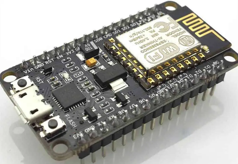
The ESP8266 is a high-performance, low-cost board developed by Espressif Systems. This board has gained popularity in the hardware community. This can be attributed to the excellent features and benefits this board offers. Also, one of the reasons it gained popularity is that it enables users to use the Arduino IDE in programming it.

The ESP8266 board is a microcontroller that allows users to use the Arduino IDE for its programming. As an SoC incorporated with an IP or TCP protocol stack, this board can offer access to any Wi-FI network. ESP8266 is mainly designed for the development of IoT applications.

It enables the connection of the internet to different applications of embedded systems. ESP8266 was designed in such a way that it offer support to IP or TCP capability. Also, the ESP8266 board can function as a standalone or a slave application. If this board is integrated as a standalone application, it functions as a microcontroller. However, if it runs as a slave, users can integrated it as a Wi-Fi adaptor.

To allow communication between the microcontroller and the ESP8266 Wi-Fi module, some AT commands are required. Therefore, ESP8266 comes with AT commands software which enables it to offer the functionalities of the Arduino Wi-Fi.

This board functions based on the L106 RISC 32-bit microprocessor core. ESP8266 needs 3.3 Volts power supply. The current consumption of this board is 100 m Amps. Therefore, it consumes less power. Also, the ESP8266 board is commonly integrated in IoT applications and robotics because of its compact size and low cost.

Creating ESP8266 PCB Design

ESP8266 PCB

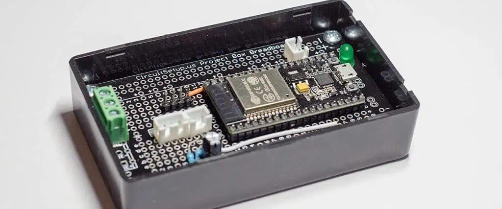
This tutorial would explain to you ways of creating the ESP8266 PCB design. We mentioned earlier that the pins on the ESP8266 are not PCB friendly or breadboard friendly. Therefore, we will be designing and developing a PCB for the ESP8266 module with all the necessary components. These components include GPIO pins and communication, connectors for power, Push button for Reset, slide switch for choosing Normal Mode or Programming Mode, and many more.

Circuit Diagram

Before we continue with the ESP8266 PCB design, you should comprehend the significance of the circuit diagram. A circuit diagram needs to be designed with all the necessary connections and components. This will make the ESP8266 PCB design process easier. So, what are the components needed for the ESP8266 PCB design? Below are all the components integrated in designing the circuit of the ESP8266 PCB board:

  • Female Headers (a few strips)
  • Two Way Slide Switch
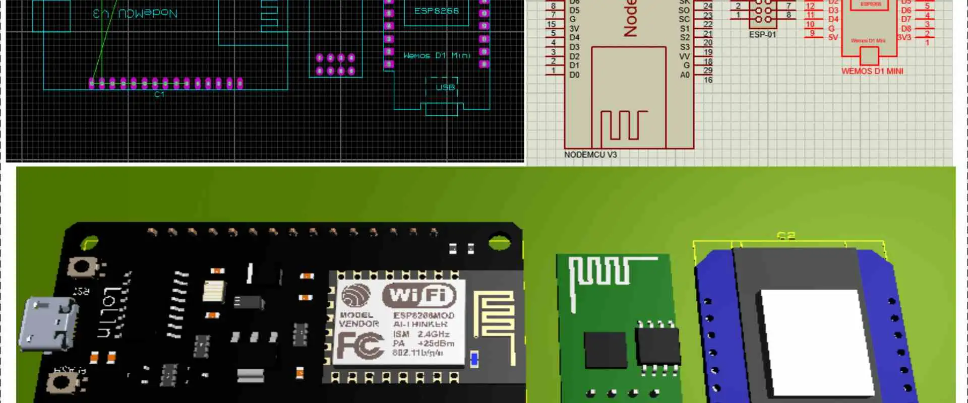
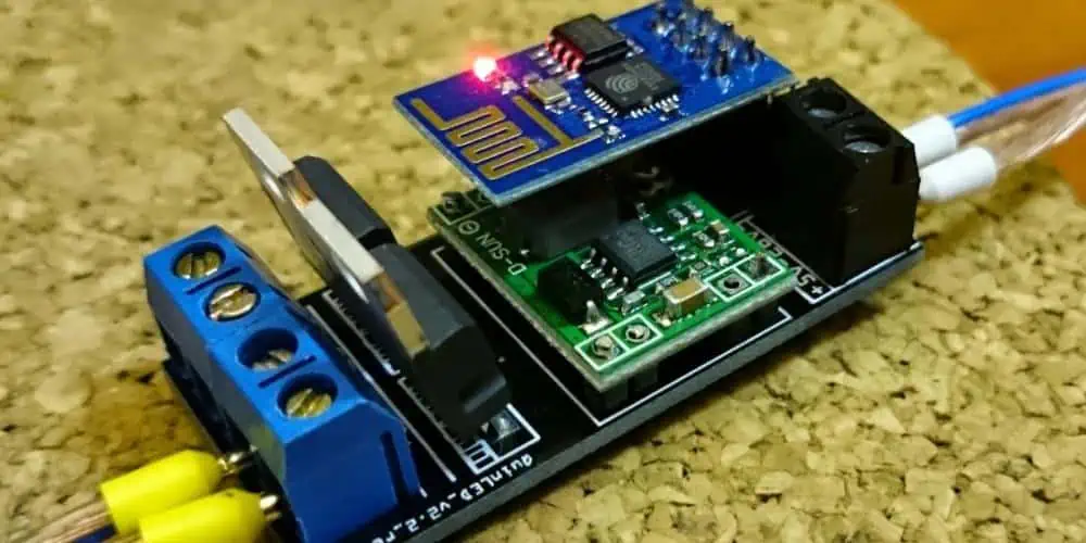
  • ESP8266 WiFi Module (ESP-01)
  • Push Button
  • 2.2 Kฮฉ Resistor (1/4 Watt)
  • 1 Kฮฉ Resistor (1/4 Watt)
  • 100 nF Capacitor

 Circuit Design

After you have designed your circuit diagram, you need a circuit design. In this phase, you need to get the pin configuration of the ESP8266. For instance, the ESP8266ESP-01 comes with 8 pins. These pins include GND, GPIOO, CH_PD, VCC, TX, GPIO2, RX, and RST.

As regards the circuit design, the CH_PCD and VCC pins of the ESP8266 are usually connected to power supply headerโ€™s VCC terminal. The GND pin is usually connected to the GND terminal. There is a 100 nF eramic disc capacitor between the GND female headers and the VCC.

The RST pin means Reset. This pin is usually linked to an end of a push button. Then the designer connects the other head of the button to GND.

It is important to know where the GPIO2 pin is connected. This pin is directly connected to any of the terminals GPIO female header while the other pin end is linked to GND.

The communication pins which include RX and TX are the next pins to connect. While the TX pin is directly linked to the communication female headerโ€™s TX terminal, the RX pin is linked via a level converter that comprises a 2.2K ฮฉ and a 1K ฮฉ resistor.

Getting Started with the ESP8266 PCB design

FULL PCB MANUFACTURING Quote

You have now understood the requirements for the circuit design and circuit diagram. So, you can proceed to the ESP8266 PCB design phase. In this case, we will be integrating the Eagle PCB software by Autodesk.

There is a need to layout the PCB designโ€™s schematic. You can make use of the circuit diagram to draw the schematic according to your desire. After you have created the schematic, you need to get started with the actual ESP8266 PCB design.  You can make use of a single layer design for this project.

Assembling the Components on the Circuit Board

After you have developed the PCB, the next phase is the assembling of components. This phase involves attaching electronic components to the circuit and soldering them. The installment of the component produces a final board. This board is then used for further applications.

After the components have been assembled, you will need to link 3.3V supply to the GND and VCC pins on the circuit board. When you are ready to program the ESP8266, you will need to use the Programming Mode position and then press the Reset button.

Since you activated the programming mode, you can start flashing the firmware. Once you have done this, press the reset button. This will make the uploaded firmware to start running.

Importance of the ESP8266 PCB Design

The introduction of the ESP8266 board has made it possible for developers and makers to create projects that are internet enables at a very low cost. Also, the popularity of the ESP8266 board led to the development of commercial boards such as Adafruitโ€™s Huzzah, NodeMCU, and WeMos D1.

ESP8266 board is integrated with RF transmitter, RF balun, analog transmitter, and power modules among others. The main benefit of the ESP8266 board is the its embedded wireless technology. This board requires no peripherals or shields. Also, it offers additional benefits like great processing power and speed. This board allows users to use the Arduino IDE to program it.

Specifications of the ESP8266

ESP8266 PCB Moudle
ESP8266 PCB Moudle

The ESP8266 specifications are as follows.

ESP8266 integrates two different serial communication protocols such as SPI ( Serial Peripheral Interface) and I2C (Inter-Integrated Circuit).

  • This board enables 10- bit analog to digital conversion
  • ESP8266 enables PWM (Pulse Width Modulation)
  • Also, it enables UART dedicated pins only and for transmission
  • It comes with a powerful Wi-Fi module with a compact size at a cheap price.
  • This board functions based on the L106 RISC 32-bit microprocessor core
  • ESP8266 needs 3.3 Volts power supply
  • The current consumption of this board is 100 m Amps. Therefore, it consumes less power
  • 3.6 volts is  maximum Input/Output (I/O) voltage
  • 12mA is the greatest Input/Output source current
  • It has a flash memory with 513 kb
  • This board can either be integrated as a station or an access point
  • It offers support to serial communication. This makes it compatible with various developmental platforms like Arduino
  • It allows users to use Lua script, Arduino IDe, or AT commands for its programming

Applications of ESP8266 PCB Design

The ESP32 board is a great alternative to the ESP8266 Wi-Fi module. However, the ESP8266 has proved to be a great option too.  

The applications of the ESP8266 board include:

  • IoT based  projects
  • Access points portals
  • Smart home automation systems
  • Wireless data logging
  • Networking fundamentals
  • Sockets and smart bulbs

Qualities of the ESP8266 PCB

The 32-bit processor featuring 16-bit instructions powers the ESP8266. Because of the Harvard architecture, instruction memory as well as data memory remains entirely independent.

The Read-Only Memory (ROM) of the ESP8266 contains a initial phase boot loader and several library code. The remaining code needs to be kept in an exterior flash memory (offers just data serial access – instead of considering the individual bytes, this user writes or reads large bytes inside the address spaces in a serial manner).

  • The quantity of flash memory that is readily available can differ depending on the ESP8266.
  • The ESP8266 contains some GPIO pins that can be used to “control” the external sensors, much like all other microcontrollers.
  • Just 11 of the ESP8266’s Seventeen GPIO pins are usable (among the 17 pins, six are utilized for communications with flash on-board memory chip). Another option is the analog input (which helps in converting a level of voltage into a form of digital value which could be stored as well as processed in ESP8266).
  • Also it features WiFi connectivity, allowing you to connect the ESP8266 to any WiFi network, access the internet, run a web service, and allow your smartphone to connect, among other things.
  • The ability to be programmed like all other microcontrollers, especially any type of Arduino, is another characteristic of the ESP8266.

ESP8266 PCB Design Functionality

The power pins

The power pins are four in number. Three pins of 3.3V and the VIN pin.

  • The NodeMCU/ESP8266 as well as its peripherals can be powered directly through VIN. The NodeMCU module’s internal regulator regulates the power provided on VIN; you also can supply 5V managed to this VIN pin.
  • An onboard voltage regulator’s 3.3V pins, which may be utilized to power external components, are its output.

GND pins

You can refer to this as ground pins of ESP8266

I2C Pins 

The I2C sensors and accessories are connected by use of pins. The I2C Master as well as Slave protocols are both supported. Programmatically implemented I2C interface function is possible, and the maximum clock frequency equals 100 kHz. It ought to be remembered that the frequency of the I2C clock should be greater than the slave device’s slowest clock frequencies.

GPIO Pins 

The ESP8266 includes seventeen GPIO pins that may be dynamically allocated to perform tasks including I2C, I2S, PWM, UART, IR Remote Controls, LED Light, as well as Button. Each GPIO with digital capability can be adjusted to a high impedance, internal pull-up, and internal pull-down. It may also be configured to level-trigger or edge-trigger when setup as an input to produce CPU interrupts it.

ADC Channel

The 10-bit precision ADC is built within the ESP8266. ADC can be utilized to implement the two tasks. These include checking the TOUT pin’s input voltage and the power voltage supply of the VDD3P3 pin. These cannot, however, be put into action simultaneously.

UART Pins

The ESP8266 includes two asynchronous UART interfaces (UART1 and UART0) that support RS485 and RS232 communication. Also, it can also communicate at about 4.5 Mbps.

You can utilize the TXD0, RST0, RXD0 and CTS0 pins on UART0 to communicate. UART1 pin only has a data transmitting signal, hence that’s why it’s typically used in printing logs.

SPI Pins

The ESP8266 has two SPIs (HSPI and SPI) that can operate in master and slave modes. The general-purpose SPI capabilities are also supported by these SPIs:

  • There are four SPI format timing modes for transfers.
  • About 64-Byte FIFO and
  • divided clocks reaching 80 MHz

SDIO Pins

Secure Digital I/O Interface (SDIO) pins of the ESP8266 are utilized to interface the SD cards directly. Both 4-bit 50 MHz and 4-bit 25 MHz SDIO-type versions are enabled.

Conclusion

The introduction of the ESP8266 board has made it possible for developers and makers to create projects that are internet enables at a very low cost. Also, the popularity of the ESP8266 board led to the development of commercial boards.

Among the most popular options for the Wi-Fi chips is still the ESP8266. Numerous professional and homemade products integrate the ESP8266 in different forms possible. This could be either as a Module or SoC. However, you need to be acquainted with both the pins as well as their functionality if you intend to design your ESP8266 PCB.

Top Advantages of Buying Bulk PCB Boards in Wholesale

universal pcb

The state of technology today is constantly improving. Electronics and devices that were unthinkable a few years ago are now commonplace in the modern world. Now, wholesale goods are the main topic of conversation. You may buy almost any kind of electronics wholesale in the UK, including devices, household appliances, and gadgets. Without a doubt, you may get any product at wholesale prices, but in this area, electronics are more common.

People’s daily use of technological devices has grown accustomed to us. Today, life is unimaginable without these gadgets and appliances.

A handful of the items, including cell phones, tablets, televisions, refrigerators, microwave ovens, and many more, are necessities of life. Other products like media players, digital cameras, and iPods are used for entertainment or possibly to stay in style. Due to the use of the most recent technology, the price of these electrical devices is fairly high.

The wholesale electronic business has grown as a result of customers’ enormous demand for electronic goods. You may now get all types of electronics at wholesale prices. Most of the time, people who own a retail business or are local distributors of anything acquire such goods in bulk. In these stores or showrooms, you can find almost every type of consumer goods. You can get your preferred electrical appliances not only from a local retailer in your town but you can also do it online.

There are a huge variety of goods available from a local retailer or online store, including televisions, stereo equipment, mobile phones, portable devices, household appliances, refrigerators, and communications equipment. Simply said, buying electronics in bulk is a significant issue today. You only need to be aware of the finest location to get these things at a discount.

Advantages of Buying Bulk PCB Boards in Wholesale 

through-hole assembly process

Projects that need electrical items are frequently constrained by budgetary restrictions. This is necessary because new items must be offered to consumers at a cost that ensures manufacturers make a respectable profit while being affordable for consumers. Purchasing electronic components in bulk is one approach to get around these difficulties. One of the smartest moves you can make in a precarious financial situation is to take it. Although the advantage of purchasing electronic components online has been mentioned, there are other advantages as well. By limiting their purchases to wholesale electronic products, consultants and comparatively tiny DIY digital fabricators can reap a variety of additional advantages. Learn more by reading on;

1. Saves Money

The first clear benefit is that buying electronic components in bulk allows you to save money. Due to the shortened supply chain, it stands to reason that purchasing components from a wholesaler will result in lower costs. You can use discounts and coupons offered by the majority of wholesalers who sell components to increase your savings and lower your component purchase costs. As an illustration, if you locate a seller offering a 10% discount and you can purchase 1000 elements, you will save significantly more money than if you had chosen to purchase only ten components. This is advantageous for your production and assembly process since it will allow you to produce devices at a lower cost per unit than other fabricators who purchase their components at retail pricing, which will benefit your consumers.

2. Customization

Customers who buy in large quantities from businesses have a role in how that element is designed. This is advantageous for any production process since it makes it simple to communicate with the firm designing a certain component and request that they create a unique model of it exclusively for you. If you decide to purchase the specified quantity of customized units, they won’t think twice about doing it because it will always be advantageous for them. Companies would not like to suffer losses from buyers who don’t mind having a component customized for them. Your finished product will benefit from having a bespoke component that is specifically designed for that function because it will perform better and likely cost less because there won’t be any compromises made, as there are when utilizing components that aren’t dedicated to specific purposes.

3. Obsolete Components

The technical industry is developing quickly, and parts that were in use a decade ago are being replaced by newer, superior ones. Yet, some of these parts had special purposes. Therefore they might be required for the creation of a particular gadget. What method do they employ? One advantage of purchasing components in bulk is that you can work with a manufacturer to have a certain quantity of the aforementioned components made exclusively for you. The majority of these businesses only consider the financial aspects of the agreement; if it is profitable for business, why would they refuse it? As they can’t start producing an out-of-date component while you only wish to acquire a few pieces, this is only conceivable if you buy the components in bulk. Where will they transport the remaining ones? Since the majority of such outdated components are not marketed or offered for sale anywhere at a reasonable price, it is simple for a producer to create an exception if you are purchasing in bulk.

4. Saves Time

While making electronic gadgets, you should put less time into finding and buying the parts and more into the actual construction. You can avoid having to frequently go back and acquire parts by making your purchases in bulk. Electronic production isn’t always a precise process, so you may occasionally require extra parts; for instance, the ones you bought are damaged while being assembled. By doing this, you can avoid having to interrupt a crucial step of the process to look for the components once more. It’s important to keep a lot of the necessary parts on hand so that any unexpected failure won’t delay the procedure because you can quickly replace them.

Thing to Consider Buying Bulk PCB Boards

FULL PCB MANUFACTURING Quote

Another reason to buy them in bulk is that not all of the components you receive were bought in your nation. It is common knowledge that a few of these imported raw materials take some time to arrive, and if the shipment is delayed, this could seriously scupper your production process. Also, shipping a lot of parts at once is more affordable than doing it separately each time you require a component.

Get the details of the parts you need before buying them in bulk if you’re buying them from abroad so that you won’t have to after a long period of time. You won’t have to go through the pain of doing it over and over again, saving you money.

ยท Availability

There are various parts that are unavailable in standard retail outlets. This is due to limited demand for them or the inefficiency of selling them in tiny numbers. Yet, because it broadens the range of components you can use, you can purchase them rapidly in bulk. This is fantastic since you may obtain the materials you require for your project.

Do your homework so that you can purchase from the appropriate wholesaler. Currently, not all dealers are trustworthy, so you should conduct your research to choose the best one. After you discover the best one, you won’t be worried about acquiring low-quality parts for your project, so you are set to go.

15 Factors that influence the growth of circuit board parts store near me

Xilinx Spartan-6 FPGA

There are many advantages to having a nearby circuit board parts store, including convenience, rapid access to knowledge, quick turnaround times, and the chance to form relationships with the staff. Local shops may have skilled personnel that may advise you and assists you in choosing the appropriate components for your project. Regular customers may also be able to bargain for lower pricing or qualify for special offers. Internet retailers may also provide many parts and expedited shipment choices.

Various variables may influence the development of a circuit board parts store close to you. These are 15 possible causes:

High rent costs:

A nearby retailer of circuit board parts may experience major development challenges due to high leasing expenses. High rent costs may hamper the expansion of such a store in the following ways:

  1. Reduced profitability: A store’s profitability may suffer greatly if its rent costs are excessive. This could hinder the store’s growth capacity by limiting its ability to invest as much in goods, advertising, or other growth prospects.
  2. Restricted cash flow: The store’s cash flow may be restricted if a sizeable amount of sales helps to pay rent. Due to this, paying for other things like personnel salaries, power charges, and inventory costs could be difficult.
  3. Decreased marketing activities: To conserve money, a store may need to scale back its marketing efforts due to high rent expenses. This may make it more difficult for the store to draw in new clients and expand its clientele.
  4. Customer pricing increases: The store could boost its prices to compensate for the hefty rent charges. In addition, lessened market competition may make it more challenging to draw in clients and increase sales.

Low-profit margins:

electronic parts manufacturer

Poor profit margins may hamper the expansion of such a store in the following ways:

  1. Restricted cash flow: A store’s cash flow may be constrained if its profit margins are low. Due to this, it could be difficult to pay bills and invest in growth prospects, such as increasing inventory or marketing initiatives.
  2. Decreased ability to compete: A store may find it difficult to draw clients and expand its clientele since rivals may be able to cut their pricing or spend more on marketing initiatives.
  3. Limited ability to invest in inventory: If profit margins are low, the store might not be able to invest as much as it would like. Customers may have fewer product options, which decreases the likelihood that they will find what they need at the business.
  4. Reduction in the store’s capacity to grow: If the profit margins are inadequate, the company can lack the resources to open additional stores or invest in brand-new business ventures like online sales or the introduction of new products.

High competition:

High levels of competition may have the following effects on a store’s expansion:

  1. Decreased market share: Due to intense rivalry, the store may struggle to draw in new clients and keep hold of existing ones. This may lead to a decreased market share, making it difficult for the store to develop and thrive.
  2. Lessened price power: The store may struggle to preserve its pricing power due to intense competition. It may be difficult for the store to defend its prices to customers if rivals sell comparable goods for less money.
  3. Restricted expansion options: Given the competition level, it could be difficult for the store to identify fresh growth prospects. It may be challenging for the store to compete and expand because rivals may spend more on marketing initiatives or have better-established online sales channels.
  4. Lower profitability: To remain competitive in an environment of intense rivalry, the store may need to lower its pricing or increase marketing expenditures. Reduced profitability, as a result, can make it difficult for the store to invest in expansion plans or pay bills.

Online competition:

These are some ways that online competition could affect your store’s expansion:

Positive effects:

  • Improved market exposure: Internet competition can make your store more visible to a larger audience. This may be especially advantageous if you sell high-end or distinctive goods.
  • Better customer experience: Online competition can push you to provide a better client experience, such as enhanced website functionality, quicker shipping, and more affordable prices.
  • Increasing your revenue streams by providing your consumers with additional goods or services might help you stay ahead of the online competition.

Negative effects:

FULL PCB MANUFACTURING Quote
  • Reduced sales: If clients choose to buy products from online rivals instead of your store, online rivalry may result in a fall in sales.
  • Price competition: Price competition can result from online competition and lower profit margins, making it more difficult for small enterprises to compete.
  • Costlier marketing: When you fight to be visible in a crowded market, online competition may raise your marketing expenses.

Limited market size:

The small market size may significantly impact the development of a nearby circuit board parts store. These are a few ways a small market could impact your business:

  1. Restricted consumer base: Your store may only be able to draw from a small customer base due to the market size. It might be more difficult to produce consistent sales and income.
  2. Low growth potential: Due to a small market, your store may not have many prospects for expansion. This may make it more difficult to grow your company and boost revenue over time.
  3. Greater competition: As there is less room for similar businesses, fierce competition may exist. It could be more difficult to stand out and draw clients.
  4. Low product diversity: Your store may have limited product diversity due to its small market size. Meeting the needs of a varied consumer base may become more difficult as a result.
  5. Price sensitivity: Customers may be more price-sensitive in a small market, making it more challenging to sustain profit margins.

Lack of marketing:

A local retailer of circuit board parts may experience severe expansion challenges due to poor marketing. These are a few ways that inadequate marketing could harm your business:

  1. Reduced visibility: Potential clients may not be as aware of your store without marketing. This may make drawing in new clients and producing steady income more difficult.
  2. Lessened client loyalty: Without marketing, your store can have difficulty cultivating a loyal following. Due to this, it could be more difficult to keep consumers and encourage repeat business.
  3. Restricted growth prospects: Without marketing, your store may only have a small window of opportunity for expansion. This may make it more difficult to grow your company and boost revenue over time.
  4. Increasing competition: Without marketing, your store may be more exposed to rivalry from businesses that have made marketing investments. It could be more challenging to stand out and draw clients.
  5. Lower profitability: Without promotion, your store can find it challenging to bring in enough money to pay expenses and turn a profit.

Poor location:

A circuit board parts store close to you may experience significant expansion challenges due to poor location. Here are some effects of a bad location on your store:

  1. Low foot traffic: If your store is in an area with low foot traffic, it could be challenging to draw in new clients and produce steady revenue.
  2. Lessened visibility: If your business is in a dimly lit region, it could be more difficult for prospective clients to locate it and learn about your goods and services.
  3. More competition: It could be more difficult for your store to stand out and draw clients if it is in an area with many competitors.
  4. Lessened client loyalty: If your store is in an unfavorable area, fostering repeat business could be more difficult.
  5. Increased costs: If your store is in a pricey neighborhood, it could be more difficult to profit and cover running expenses.

Lack of expertise:

A lack of competence may significantly hamper a nearby circuit board parts store’s expansion. The following are some effects that a lack of knowledge may have on your store:

  1. Restricted product selection: You can find it difficult to provide a broad selection of products to satisfy your client’s needs if you lack knowledge of circuit board parts.
  2. Lessened customer confidence: If you lack experience, your clients can have less faith in your capacity to deliver high-caliber goods and services.
  3. More returns and complaints: If you lack experience, you may be more inclined to sell customers things unsuitable for their needs, which could result in more returns and complaints.
  4. Restricted expansion prospects: Without competence, you would not have many chances to broaden your product line and boost sales.
  5. Increased expenditures: If you lack experience, managing your store may need hiring more workers or consultants, which could increase your operating costs.

Limited product selection:

A limited product variety may significantly impact the development of a circuit board parts store close to you. Here are a few ways why having a small assortment of products could harm your business:

  1. Lower customer satisfaction: Without a large product range, your clients can have trouble finding what they require. It could cause unhappiness and a negative customer experience.
  2. Lost sales opportunities: If you have a limited assortment of products, clients may go elsewhere to buy what they need, which could result in missed sales opportunities.
  3. More competition: You can have increasing competition and find it difficult to stand out if other retailers in your neighborhood provide a wider assortment of goods.
  4. Restricted expansion opportunities: Without a large product assortment, you might only have a few options for growing your company and boosting sales.
  5. Decreased profitability: Without a large assortment of products, you can find it difficult to bring in enough money to pay your bills and turn a profit.

Poor customer service:

A local store selling circuit board parts may have severe expansion barriers due to poor customer service. Here are a few ways that subpar customer service could harm your business:

  1. Decreased consumer satisfaction: Unsatisfied customers can lead to lost revenue and a bad reputation for your company, resulting from poor customer service.
  2. Unfavorable reviews and word-of-mouth: Disgruntled consumers may post unfavorable reviews or spread the word about their bad experiences.
  3. Decreased consumer loyalty: Customers who receive poor service may decide to shop elsewhere, weakening customer loyalty.
  4. Lost sales opportunities: If your customers have a negative shopping experience, they can be less likely to return or refer others to your store.
  5. Heightened competition: If other businesses in your community provide better customer service, you can encounter more opposition and find it difficult to distinguish.

Lack of inventory management:

Poor inventory management can significantly hamper a circuit board parts store’s expansion.

  1. Lost sales: Customers may shop elsewhere if the retailer does not have the proper products in stock. This can result in fewer sales and lower revenue.
  2. Higher costs: Inadequate inventory control can result in either overstocking or understocking, which can be expensive. Understocking can result in urgent orders and higher shipping costs while overstocking can tie up funds and occupy precious storage space.
  3. Lower customer satisfaction: Disgruntled customers may decide to shop elsewhere if they can’t find what they’re looking for at the store. Reduced consumer loyalty and satisfaction may result from this.
  4. Reduced effectiveness: It might be challenging to determine which products are selling well and which are not without efficient inventory management. This could result in inefficient ordering and stocking, which would have a negative financial impact on the store.
  5. Improper inventory management might make it challenging to predict the demand for products in the future. This may result in either overstocking or understocking, affecting sales and earnings.

Poor financial management:

Poor financial management can significantly hamper a circuit board parts store’s expansion.

  1. Inability to invest in growth opportunities: Bad financial management can leave no money for investments in expansion opportunities. The store may be unable to expand and remain competitive as a result.
  2. Trouble managing cash flow: Without sound financial management, the shop can find it difficult to control its cash flow. This could result in a cash flow problem that makes it difficult for the store to pay its bills.
  3. Higher costs: Inadequate money management can raise costs due to missed payments or interest charges on a credit card or loan debt. These expenses may reduce profits and impede development.
  4. Inability to make data-driven judgments: The retailer may struggle to make commercial decisions without reliable financial data. This may result in bad choices and a lack of development.
  5. Bad credit rating: Bad money management can result in a bad credit rating, making it challenging to get credit or loans in the future.

Lack of partnerships:

The absence of partnerships can hinder the expansion of a retailer of circuit board parts in several ways:

  1. Restricted access to new clientele: Without partnerships, the store may have just a small number of potential new clientele. It could be challenging to expand the store’s clientele and boost sales.
  2. Restricted product selection: Partnerships can help a store increase selection by promoting complementary goods from affiliated businesses. Without collaborations, the business could only have a few possibilities for growing its product selection.
  3. Restricted brand exposure: The store can boost its brand exposure by forming partnerships with bigger or more well-known brands. Without collaborations, the store could only have a few opportunities to raise brand exposure and recognition.
  4. The store has limited resources for innovation; partnerships can give it access to resources for new technologies, research, and development. It can help it innovate and maintain its competitiveness. Without partnerships, the retailer might not have as much money to spend on innovation.
  5. Increased competition: Without partnerships, the store can experience increased opposition from bigger businesses. They can provide a greater selection of goods and services thanks to their partnerships.

Changes in the industry:

A nearby store selling circuit board parts may experience tremendous growth due to changes in the sector. Here are a few possible ways that shifting industry dynamics can impact the expansion of your neighborhood circuit board parts store:

  1. Technological developments: Technological developments may modify the kinds of circuit boards and parts required. It affects the demand for some of the store’s products. On the other side, the shop could have to change its emphasis to more recent technology if specific circuit boards become outdated to remain relevant.
  2. Rival behavior: The development of a business can also depend on the actions of competitors in the market. 
  3. Economic circumstances: Economic circumstances can significantly impact consumer demand for circuit board components. The shop might see a boost in demand for its goods if the economy is booming and more companies and people are making technology investments. Nonetheless, the shop may see a fall in sales if the economy is struggling and customers are cutting spending.
  4. Disruptions in the supply chain: Disruptions in the supply chain might affect the accessibility of the store’s goods. This may hinder the store’s expansion, causing lost revenues and irate customers.

Summary

A nearby retailer of circuit board parts could need to look towards other growth prospects. It includes online sales, to extend its product line or discover ways to lower rent costs. The store may need to differentiate itself from rivals by providing higher customer service, exclusive goods, or distinctive value propositions. Also, a small market might make it difficult for the business to expand and survive. So, it may be beneficial to concentrate on solidifying your relationships with current clients. As a result, it increases your product selection and develops innovative ways to sell your business to a larger audience. Also, a small product variety and a lack of experience may drastically restrict the store’s ability to expand.

Bad customer service can also act as a barrier to growth. So, it’s essential to establish customer service standards and procedures. In addition, partnerships may restrict a business’s access to new clients, resources for innovation, and resources to compete effectively. As a result, the success of a store depends on its capacity to adjust to these changes.

What are the Types and Applications of the Digikey PCB?

Digikey pcb

With its headquarters in Minnesota, in the United States, Digi-Key Electronics is known for being a global leader in high-service electronic components distribution as well as automation products. Being the industry’s first innovator, Digi-Key offers over 14.9 million different components from more than 2,400 reputable name-brand producers, with industry-leading depth and breadth of product within stock and ready for rapid dispatch.

Digi-Key offers design engineers as well as procurement specialists a multitude of digital resources and options in addition to the products which fuel technological innovation, helping them to do their jobs more effectively.

YouTube video

What is Digikey PCB?

The usual term for the empty board that you provide us having your layout data and then utilized for the mounting of the components once it has been delivered to your doorstep is called the Printed Circuit Board or PCB.

Using conductive paths, tracks, as well as signal traces which are etched out of copper sheets then laminated to the non-conductive substrates, a PCB, serves to support mechanically as well as electrically link electronic components.

What are the Types of Digikey PCB?

Frequency, the amount of layers, as well as the substrate utilized are frequently used to categorize Digikey PCBs. Below are a few common types addressed.

Single-sided PCBs

Circuit boards just with one substrate layer as well as base material, are known as single-sided PCBs. The thin metal layer, for example, copper that conducts electricity properly is applied over this layer. In addition to the silk screen finish, the layer of copper on these PCBs additionally has a protecting solder mask put on top of it.

The following are some benefits of single-sided PCBs:

  • Single-sided PCBs serve the purpose of mass production because they are inexpensive.
  • Simple circuits like power sensors, sensors, relays, and electrical toys use these Boards.

Double-Sided PCBs

With double-sided PCBs, the conductive layer, made of metal, is present on the substrate’s two sides. The metal components can be connected through one side onto another using holes inside the pcb board.

These Boards use any of the mounting techniquesโ€”thru-hole technology or SMT technologyโ€”to link the circuitry along either side. Through-hole technology entails inserting lead components that are soldered onto the pads somewhat on opposing sides via the already-drilled holes present on your circuit board.

Electrical components are directly mounted on the circuit boards’ surface using SMT technology. The following are benefits of using double-sided PCBs:

  • Comparing surface mounting to through-hole mounting, more circuits can be added to the circuit board.
  • These circuit boards are used in many different applications, such as mobile phone systems, power monitoring systems, amplifiers, test equipment, and many more.

Multi-layer PCBs

FULL PCB MANUFACTURING Quote

PCBs boards with at least four copper layers, such as 4 layers, 6 layers, 8 layers, etc., are known as multi-layer PCBs. These PCBs advance the double-sided PCB technology. With multilayer PCBs, these layers are separated by insulating materials as well as several substrate layers of the board. The PCB come with a small size and are advantages in terms of available space and weight. Many benefits provided by the multi-layer PCB include:

PCBs with several layers provide a great deal of design versatility.

With high speed circuitry, these PCBs are crucial. They give conductor pattern as well as electricity greater room.

Rigid PCBs

PCBs that are referred to as rigid are those in which the base material was made from solid material that cannot be folded. Some key benefits they provide include:

  • Because these circuit boards are small, it is possible to build a wide range of intricate circuitry around them.
  • Given that every component on the rigid PCBs is clearly identified, they are simple to repair and maintain. Moreover, the signal routes are well-structured.

Flexible PCBs

The flexible base materials are used to build flexible PCBs. There are single-sided, double sided, as well as multilayer versions of these Boards available. This aids in minimizing the device assembly’s complexity.

These PCBs have a few benefits.

  • These PCBs significantly reduce board weight while also saving considerable space.
  • Flexible PCBs aid in reducing board size that makes them perfect for a variety of applications that require substantial signal trace densities.
  • These circuit boards are made to function in environments whereby density and temperature are crucial considerations.

Rigid-Flex-PCBs

Circuit boards that combine flexible and rigid materials are known as rigid flex Circuit boards. They are made up of several stiff boards linked to numerous layers of the flexible circuitry. These PCBs were carefully constructed. As a result, it has a variety of military and medical uses. This PCB provides a 60% reduction in space and weight thanks to their lightness.

High-Frequency PCBs

In the range of frequency of 500MHz to 2GHz, high-frequency Digikey PCBs are employed. Several frequency-critical applications, including communication systems, microstrip PCBs, microwave PCBs, etc., use these PCBs.

Aluminum-backed PCBs

Due to the aluminum construction’s ability to dissipate heat, these Digikey PCBs are employed in applications requiring considerable power. The high rigidity level and low amount of thermal expansion that aluminum-backed Circuit boards are recognized for providing makes them the perfect choice for applications requiring a high level of mechanical tolerance. Power supply and LEDs are both used with PCBs.

Applications of Digikey PCBs

SSD PCB
SSD PCB

Consumer electronic devices

Among the most popular products that use PCBs include Smartphones, PCs, and Internet of Things (IoT) devices like smart speakers. PCBs are widely used in household gadgets like refrigerators and microwaves.

More and more IoT-compatible devices will require PCBs as well. Due to the numerous and intricate requirements of such device, PCBs used in gadgets like Smartphones as well as home assistants must be compact and have connections of high density.

Automobile components

Compared to earlier models, modern cars depend far more on electrical operations. These systems employ a variety of distinct PCBs in order to function properly. Parking as well as proximity sensors, video and audio systems, navigation systems, engine management system, resource management and monitoring, as well as fuel regulators are all implemented using automotive PCBs.

Modern automobiles include a large number of intricately coupled sensors that are dependent on numerous complex high frequency circuit boards to operate. PCBs would be increasingly more in demand as the industry development continues, particularly with the advent of the electric vehicles.

Medical equipment

Many uses for Digikey PCBs can be found in the healthcare sector. They are utilized in implants as well as internal devices like pacemakers, as well as in systems for medical imaging like ultrasound, CAT and CT scanners, as well as in monitor technology measuring vital signs like heart rate and blood pressure. Since these PCBs must be extremely compact and adhere to stringent sanitary standards, they are high-density interconnect or HDI types.

LEDs

Because of their small size, high energy efficiency, as well as extended lifespan, LEDs are indeed the preferred lighting technology in many industries. LEDs are used in smart lighting, electronic billboards, car displays, including laptop screens.

Using LED technology, Circuit boards are used to transmit heat out of the light source, which could also otherwise reduce the lifespan of the LED. In all these applications, PCBs are often created using aluminum that helps in the effective transfer of heat compared to the remaining metals.

Aerospace

Boards that are flexible are crucial to aerospace technology. Rigid PCBs are easily harmed by the intense turbulence that aerospace vessels experience when in flight. Contrarily, flexible PCBs were made to be lightweight and damage-resistant to vibration.

A variety of aircraft applications, including monitoring equipment, power supplies, and communications equipment, use these highly functional and precise Circuit boards.

Industrial equipment

PCB electronics are used to drive industrial equipment like powerful presses and drills, as well as machinery used to monitor and regulate factors like temperature and pressure throughout manufacturing.

An Overview of Digikey’s PCB Manufacturing

Making or manufacturing PCBs is a sure difficult procedure which starts with the product idea and finishes with a very functional circuit board assembly.

During the process, the schematic is made to represent the network connectivity, a Circuit board design is constructed, and electronic parts are purchased. This circuit board is going to go into the entire system after these components are soldered on to the board as well as after assembly, tests, and verification are finished.

There are numerous complex steps which have to be done for a PCB to be successful. The creation of the blank board is one step in the process which doesn’t receive the credit it merits. Due to this sophisticated software tools required for its construction, the PCB design attracts much attention. Manufacturing would receive equal praise for producing the end product.

The enigmatic process of pcb board fabrication, which is frequently unknown outside the design community, is however somewhere inside the center of this.

Conclusion

Expert application engineers are employed by Digikey to assist clients with the design phase. They concentrate on frequent problems that can increase costs and decrease productivity when engaging with clients. All Digikey PCB offerings are eligible for their services, which guarantee that each customer obtains high-quality items within their price ranges.

Top 14 electrical cable manufacturers in the world

Electronic Cable Assemblies

The process of creating cables to transport electrical power or communications is called electrical cable manufacture. Wire drawing, stranding, insulation, jacketing, shielding, and testing are some of the phases involved. The final cable is put through several tests to ensure it satisfies the requirements for electrical performance, mechanical strength, and durability. This procedure may change depending on the type of cable, the intended usage, and the materials used.

The rankings of the top electrical cable manufacturers may change depending on the metrics used to assess them. Below are 14 of the biggest and most respected producers of electrical cables, listed alphabetically:

W. L. Gore & Associates, Inc.

Another area of expertise for W. L. Gore & Associates, Inc. is the production of electrical cables. The business manufactures a variety of high-performance cables and cable assemblies utilized in various sectors, including telecommunications, aerospace, and defense.

Electrical cables made by Gore deliver fast data transfer, dependable signal integrity, and toughness under challenging conditions. High-speed data cables, microwave/RF assemblies, power cables, and aircraft cables are among the company’s offerings. Moreover, Gore cables are renowned for their excellent shielding efficiency, low attenuation, and durability to corrosive substances, abrasion, and freezing temperatures.

It offers engineering services, such as cable design and prototype, as well as testing and certification services, in addition to its cable products to guarantee that its cables meet or surpass industry standards and client needs.

Gore has created novel cable designs that have raised the bar for performance and dependability. As a result, well-known applications, including the Mars Rover, the Hubble Space Telescope, and the Large Hadron Collider, among others, have used the company’s cables.

YouTube video

Lapp Group

German-based Lapp Group is a worldwide corporation that produces cables, wires, and cable accessories for automation, mechanical engineering, and industrial applications. Oskar Lapp established the business in Stuttgart, Germany, in 1957.

Lapp Group offers a variety of products, including fiber optic cables, Ethernet cables, control and power cables, and data cables. Moreover, the business provides specialized cable solutions, cable management programs, and cable extras, including connectors, glands, and marking devices.

Lapp Group has production facilities and sales offices worldwide, including Europe, Asia, North America, and South America. The business is strongly committed to sustainability and has taken several steps to lessen its negative effects on the environment, including adopting renewable energy sources and cutting back on waste and emissions.

Nexans

FULL PCB MANUFACTURING Quote

A French multinational corporation, Nexans, specializes in producing and distributing electrical cables and related goods. The business, which has its headquarters in Paris, France, was established in 2000 due to the union of two major cable producers, Alcatel Cable, and Nexans.

Power cables, control cables, instrumentation cables, communication cables, and fiber optic cables are just a few of the many cable products Nexans offers. Together with installation and maintenance services, the business also offers cable accessories, including connectors, terminations, and jointing kits.

Nexans works internationally with facilities and sales offices across more than 50 countries. The business has a strong commitment to sustainability. It has taken several steps to lessen its negative effects on the environment, including creating eco-designed goods and lowering its carbon footprint. Nexans also makes research and development investments to provide cutting-edge cable solutions for several industries, including energy, transportation, and construction.

Prysmian Group

An international company with its main office in Milan, Italy, Prysmian Group focuses on producing cables and systems for the energy and communications industries. Two top cable producers, Prysmian and Draka, merged to establish the business in 2011.

Prysmian Group employs over 29,000 people and operates in more than 50 nations. The company provides a wide range of goods. They include high and medium-voltage cables for power transmission and distribution, optical fibers and cables for telecommunications, submarine cables for offshore wind farms, and specialized cables for various industrial uses.

The business is well renowned for its emphasis on research and development. It has various sites worldwide specifically for that purpose and relationships with top research institutions and universities. In addition, the Prysmian Group values sustainability and has established challenging objectives for lowering its environmental effect and fostering moral and responsible behavior throughout all of its businesses.

One of the biggest cable producers in the world, Prysmian Group serves clients in the energy, telecommunications, construction, and transportation sectors. It is a component of the FTSE MIB index and trades on the Italian Stock Exchange.

Southwire Company, LLC

RF cable

Leading producers and suppliers of wire goods, including electrical and communication cables, are Southwire Company, LLC. Roy Richards Sr. established the business in Carrollton, Georgia, in 1950, and its headquarters remain there.

In addition to building, industrial power cables, automobile, telecommunications, and utility transmission and distribution cables, Southwire manufactures various other wire and cable products. Also, the business produces and sells a variety of electrical tools, gear, and accessories.

Southwire is renowned for its dedication to sustainability, corporate responsibility, and industrial activities. The corporation has a variety of environmental and social objectives, such as lowering its carbon footprint and fostering inclusiveness and diversity among its employees.

One of the US’s biggest wire and cable makers is Southwire, a privately held business. It has several production sites nationwide, a North American-wide distribution network, and some overseas markets.

Sumitomo Electric Industries

Japanese multinational company Sumitomo Electric Industries, Ltd. is in Osaka. The Sumitomo Group began the business in 1897. Since then, it has expanded to become a top producer of various goods, including electrical wire and cable, optical fibers and components, electronics, automotive parts, and industrial materials.

Across several areas, including the energy, telecommunications, and automotive industries, Sumitomo Electric Industries is renowned for its technological prowess. The company’s products are helpful in various applications, including power transmission and distribution, telecommunications networks, and electronic gadgets.

Sumitomo Electric Industries offers a variety of energy-related solutions, such as power cables and wires, transformers, and energy storage systems. In addition, the business provides optical fibers and parts for high-speed data networking and transmission in the telecommunications industry.

A significant player in the automobile sector is Sumitomo Electric Industries, which offers a variety of systems and parts, such as electronic control units, engine components, and wire harnesses.

The business is dedicated to sustainability and has established challenging objectives for lowering its environmental footprint and fostering social responsibility. With operations in more than 40 countries and a staff of more than 280,000 people globally, Sumitomo Electric Industries has a footprint worldwide.

The Okonite Company

The Okonite Corporation is an American manufacturer of electrical cables and wires used in various sectors. They include communication and control systems, power production, transmission, and distribution. E. T. Hall established the business in Paterson, New Jersey.

The Okonite Company is known for making sturdy, high-quality cables and wires to satisfy its clients’ exacting demands. Power and control cables, instrumentation cables, communication cables, and specialized cables are just a few of the many things the business provides. Products from Okonite are helpful in a wide range of settings, including petrochemical factories, hospitals, airports, railroads, and power plants.

To fulfill particular client needs, Okonite also provides bespoke cable design and engineering services in addition to its conventional product offerings. In addition, the business values research and development to continually enhance its goods and services.

The Okonite Corporation has a long history of quality and innovation, and many businesses that need dependable and secure electrical cables and wires rely on its products.

TPC Wire & Cable Corp.

TPC Wire & Cable Corp designs and produces high-performance wire and cable products. Additionally, it has its corporate headquarters in Macedonia, Ohio. TPC is a well-known provider of industrial-strength wire and cable products to various sectors, including oil and gas, mining, automotive, and industrial automation.

Power and control cables, instrumentation and thermocouple cables, high-temperature cables, flexible and portable cords, and bespoke cables are just a few things the business offers. TPC Wire & Cable products can endure abrasive conditions and high temperatures, making them perfect for use in demanding applications.

TPC Wire & Cable provides various value-added services in addition to its goods, such as custom cable design, engineering assistance, and cable assembly services. The business has established a reputation for excellence in the wire and cable sector by committing to offering its clients superior goods and first-rate customer service.

ABB

ABB is a provider of digital technologies focusing on electrification, motion, and industrial automation products, systems, solutions, and services. It offers customers in the utilities, industry, transport, and infrastructure sectors. They operate in Asia, the Americas, the Middle East, Africa, and Europe industrial equipment and systems.

Turnkey solutions are provided by ABB’s cable system and cable accessory division. It also includes design, engineering, supply, installation, commissioning, and servicing. Karlskrona, Sweden, employs around 1,000 people and contains cutting-edge production and R&D facilities for high-voltage submarine and underground cables. A brand-new, state-of-the-art cable-laying vessel that is now under construction is also in the transfer of assets.

For over 60 years, ABB has provided utility and business clients a full spectrum of technical equipment, services, and solutions in automation and power technology. Additionally, they have a significant presence over the whole nation.

Belden Inc.

High-performance cable solutions from Belden Cables are transforming the look of contemporary manufacturing facilities, production methods, and industrial infrastructure. In addition, they can deliver dependable communications wherever in between, including between management and staff, factories, and corporate headquarters.

Belden provides a variety of cables, including Ethernet, fiber optic, electronic wire, VFD, audio, instrument, Fieldbus, and more. A cable of type 3 In addition to a choice of logarithms from 2 to 400 risers and plenums, ATMM (corrugated aluminum strip) variants of Belden’s DataTwist 3 are also available for improved crush resistance. In locations where costs are a concern we use IP applications, and category 5e cables offer the highest network performance and stability.

Each level of performance offered by category six cables surpasses that of TIA-568-C.2 while providing excellent performance with ample headroom. In addition, using bonded-pair technology makes installation as robust as feasible. Belden creates, produces, and sells technology and goods related to networking, security, and connectivity. One of the most reputable industrial cable producers in the world is Dekoron Wire & Cable LLC. Wire and cable are produced and distributed by Basic Wire and Cable.

CommScope

High-performance fiber connection is produced by CommScope utilizing a wide range of materials. In addition, they invest in their R&D work to optimize performance while upholding the highest quality and safety standards in their cable goods.

Since 2016, they have collaborated with BASEC for their cable testing and certification requirements. Additionally, they have chosen to work with BASEC for the higher classification AVCP Systems 1+ CPR certifications. This thorough assessment method ensures that the facilities and goods meet the necessary standards. In addition, exceeding the minimal criteria gives customers and end users more certainty that the cables won’t aid in spreading flames in the case of a fire, protecting both persons and property.

Corning Inc.

Corning produces and sells specialty glasses, ceramics, and other related materials. The business sells glass substrates for LCD televisions, desktop monitors flat-panel options, notebook computers, and laptops. It also sells hardware, cable, optical fibers, and tools for the telecommunications networks, filters for automotive, ceramic substrates and diesel applications, serum, glass and plastic labware, and tools for discovering drug. Furthermore, it produces specialized glassware and sophisticated optics for consumer electronics, semiconductor, aerospace & defense, optical, and telecommunications industries. Africa, the Middle East, Asia-Pacific, and the Americas are all places where the corporation conducts business. The city of Corning in New York, serves as the headquarters of Corning.

Corning Cable Systems provides the widest selection of end-to-end fiber optic and copper product solutions for clients worldwide telecommunications networks. Its customer-focused solutions include cables, connectors, associated hardware, and network services. They stand as a global telecom business leader because of their dedication to excellence and exceptional client satisfaction.

Hitachi Metals

A Japanese multinational corporation, Hitachi Metals, focuses on producing and marketing metal goods, including steel, copper, and aluminum. The corporation has its headquarters in Tokyo, Japan.

For various applications, including usage in rolling stock, Hitachi Metals manufactures and markets a selection of electrical wires, cables, and associated materials. Our wide spectrum of consumers appreciates and acknowledges our products’ reliable quality.

Rolling stock’s usefulness is significantly improving over recent years. This increases the amount of data transferred while trains operate, necessitating rolling stock telecommunication links with ever-improving performance.

In addition to producing wire and cables for rolling stock, Hitachi Metals provides services for rolling stock and harness assembly based on design data. As a result, Hitachi Cable Europe s.r.osystem strengthens with the addition of harness assembly lines. It enables it to provide solutions that assist rolling stock manufacturers in Europe in lowering labor costs and fabrication times.

TE Connectivity

A maker of connectors, relays, fiber optic cable, wireless components, and touch displays with a presence all over the world is TE Connectivity. During its 75-year existence, TE Connectivity has created and produced over 500,000 items. TE Connectivity products can help you satisfy your wire and cable requirements. This is for electronics necessary in the toughest conditions and demanding applications. Their materials science and EMI shielding expertise enable them to provide the ideal solution. It balances the necessary qualities for fit, shape, function, performance, and dependability.

Moreover, TE Connectivity aids businesses in the creation and improvement of electrical components. They produce performance-efficient connection and sensor solutions through collaboration with clients and partners. Reliability, durability, and the will to keep driving forward were the focal points of the collaborative efforts.

TE Connectivity provides high-performance wire and cable.

How to make a Flexible PCB at Home

quick turn flexible PCB prototype

Printed Circuit boards are significant components of most, if not all, electronic and electrical components. These components dominate the electronic and electrical industry due to their ability to help manufacturers generate compact gadgets that are powerful and efficient. Moreover, due to their compact size, they make the packaging process easier and more effective.

However, out of the many different types of PCBs that exist, flexible PCB top the list in terms of printed circuit boards that offer impeccable space efficiency. Due to their ability to curve into various shapes, manufacturers utilize them to make pretty tiny gadgets such as hand-held gadgets and wearables. However, even though flex PCBs are efficient, their production process can be rather complex due to the flexibility of the components that technicians utilize to make these circuit boards. However, did you know that with the proper guidance, you can make a flexible PCB at home? Here are some instructions to help you generate your flexible PCB in the comfort of your home.

What is a Flexible Printed Circuit Board?

flexible pcb circuit board

Before we move on to how you can generate a flexible printed circuit board at home, let us first look at what a flex PCB entails.

Generally, flex PCBs feature a combo of different types of PCBs and various flexible materials. Therefore, these popular printed circuit boards go by multiple names, which include flexible circuit boards, flex circuits, flex PCBs, and flex circuit boards. Moreover, technicians utilize the same elements that they utilize to make rigid circuit boards to generate flexible PCBs, only that the elements they use in flexible PCBs are flexible, which results in a flexible PCB.

YouTube video

Types of Flex PCBs

Flex PCBs come in many variations due to various specifications and configurations that technicians make during production. However, when it comes to classification, we classify them according to their configurations and layers as follows:

Flex PCBs as Per Configuration

When it comes to classification via configuration, you can group flex PCBs as follows:

HDI Flex Printed Circuit Boards

HDI (high-density interconnect) printed circuit boards are flex PCBs that cater to applications that require high-performing flex printed circuit boards. Due to their build, they tend to have impeccable performance compared to other circuit board types.

The design of an HDI flex printed circuit board incorporates several features, including micro-vias. Moreover, these circuit boards provide better construction, designs, and layouts.

Generally, these circuit boards use thinner substrates when compared to regular flex-printed circuit boards. Due to these features, these flex PCBs help manufacturers reduce costs in terms of procuring raw materials. Moreover, they also end up having reduced package sizes which helps during shipment and application in generally smaller gadgets.

Rigid Flexible Printed Circuit Boards

Rigid flexible printed circuit boards are typically hybrid printed circuit board that combine the features of a rigid and a flexible printed circuit board.

These variation of flexible printed circuit boards is pretty popular since it bring the best features of both worlds.

Classification of Flex PCBs Using Layers

FULL PCB MANUFACTURING Quote

The classification of flex PCBs using layers groups the various flexible PCB types into the following categories:

Single sided flex Printed Circuit Boards

The single-sided flex PCB is basically among the most basic variation of flex PCBs. That is because this flex PCB variation only has one layer of flex polyimide film and a slim layer of CU (copper). Moreover, the conductive layer is only accessible via the top part of the circuit board.

Single Sided Flex PCBs with Dual Access

Single-sided flex PCBs with dual access are simply single-sided flex circuit boards that are designed such that you can access the conductive layer via both sides of the board.

Double-sided Flex PCBs

Double-sided flex PCBs typically feature two copper conductive layers, which technicians place on either side of the polyimide or substrate layer. To make electrical connections between two copper conductive layers, technicians utilize a method known as THT (through hole).

Multi-Layer Flex PCBs

Multi-layer flexible PCBs are generally a combo of multiple single-sided and double-sided flex circuit boards. To make interconnections within these circuits, technicians utilize various technologies, which include:

Main Benefits of Working with Flex PCBs

Over time, flex PCBs have become pretty popular due to their multiple benefits. Here are some of the most common benefits of flex printed circuit board:

Reduce Package Size

Generally, flex PCB can easily fit into multiple applications where other PCB types might not work efficiently or at all. That is because these circuit boards are typically lightweight and thin. Moreover, you can easily fold, crease and position these circuit boards in various areas that are space deficient. Moreover, due to their slim size, they end up generating a small package that is easy to ship.

Accurate Designs

Manufacturers primarily utilize automated machinery to effectively assemble and design printed circuit boards. The utilization of these gadgets helps in terms of reducing errors that tend to occur due to harnesses and hand-built cables. Moreover, these gadgets ensure impeccable accuracy, which is crucial when dealing with printed circuit boards.

Design Freedom

The designing process of PCB isn’t limited to merely two layers. Due to their flexibility, these circuit boards provide PCB designers with a lot of freedom when it comes to designing them. Moreover, PCB designers can choose to either go with single-sided flex PCBs, double-sided flex PCB, or multi-layer flex PCBs when generating their designs.

The flexibility that comes with flex PCBs also makes them perfect for applications that require multiple interconnections with complex configurations. Moreover, you can design your flex PCB to cater to both SMT components and THT components.

High-Density Config

Flex-printed circuit boards can encompass a mix of surface mount and thru-hole components. By utilizing this feature, you can easily generate a flex PCB that can accommodate high-density gadgets with narrow separation within the layers. Moreover, you can also design lighter and denser conductors, freeing up space to accommodate additional components.

Flexibility

Flex PCBs can easily connect with various planes when operational. Doing so helps in terms of reducing space and weight issues that most people face when working with rigid printed circuit boards.

Steps to Generate a Flexible PCB at Home

flex-circuit-manufacturer

If you are looking to generate a flexible printed circuit board at home, here are the steps to follow:

Get a Copper Coated Film

To start off, you’ll need to purchase a thin sheet of polyimide bearing copper on either both sides or simply one side depending on the type of flex PCB you want to generate. Typically, polyimide sheets are yellow, and they have high melting points. Moreover, people sometimes refer to this component as Kapton. Furthermore, copper-coated polyimide tends to come in many variations, but the most common type is DuPont material.

DuPont sheets also generally come in different variations due to varying copper thicknesses, adhesive thicknesses, and polyimide thicknesses in general. CU or copper thickness is usually given in mils, where one mil is typically equal to 0.001 inches.

For this project, you can utilize a Dupont LF7062, which has 0.5 mils of adhesive, 0.5 oz of copper, and about one mil of Kapton. However, you can still go for more variations since this type of film tends to be crinkly and a bit thin. For instance, you can go for the Dupot LF9210, which contains one mil of Kapton, one mil of adhesive, and 2 oz of copper.

Other variations include double-sided CU with rough surfaces. These variations are typically denoted by the letter R.

After obtaining the sheet, you have to cut it to fit the following dimensions:

  • 8.5 by 14 inches
  • 8.5 by 11 inches

Do not smudge the copper using oil or fingerprints during the cutting process. Doing so can easily block the etching solution later on. Moreover, to shield the printer from damage, try to flatten the sheet’s edges.

Utilize a Solid-Ink Printer

To print directly onto the CU film, you must work with a solid-ink printer. These printers look pretty similar to laser printers. However, they usually utilize melted wax to print rather than ink. Moreover, the wax that this printer utilizes to print makes a perfect shielding layer for CU (copper) etching. And unlike most laser printers, this printer does not rely on charging the paper’s surface since this could lead to issues when you change the paper and replace it with copper sheets.

Here are some solid-ink printer models that you can find in the market:

  • Xerox Phaser 8860, 8560, 8500, 8400 and 8200
  • Tektronix Phaser 860, 850 and 840

Most Phaser solid-ink printers also function like regular laser printers. However, they do have a hood that contains a solid ink block.

If you can’t access a solid ink printer, you can use the toner transfer method, which utilizes laser printers.

Print your Design on the Pyralux

flex pcb
flex pcb

Once you have your solid ink printer up and running, it is time to print your design on the copper film. To do so, you must first draw the design using a graphics program like CAD. Once the design is ready, you can utilize the manual feeding tray to effectively print the design onto your copper sheet in black. You can also utilize various color variations, which include:

  • Yellow
  • Magenta
  • Cyan
  • Green
  • Red

However, you should avoid colors that have light shades. These colors will not bring out your design clearly on the board.

During the printing process, you should utilize photo or high-resolution mode, which is usually available in the setup area of your graphics program. Generally, the high-resolution mode tends to print in a slow manner when compared to the standard printing mode. However, it is more efficient and promotes impeccable adhesion of the wax to the copper.

Most phaser printers usually print the copper sheet with the copper side facing down. However, when it emerges at the other end, it does so with the copper sheet in an upside-down position.

If the printer’s feed cog faces some issues grabbing the sheet, you can give it a slight shove to help it out. However, it would help if you were gentle to avoid damaging the copper sheet.

Etch your Copper Sheet

Once you are done with the printing step, you then have to insert the copper sheet inside the ferric chloride for about 5 minutes. When using the etchant, avoid getting the chemical on your skin or eyes.

The etching time typically depends on various conditions, which include:

  • The thickness of the copper
  • The temperature and more

Due to these variations, you should keep checking on the board when it is inside the etchant to ensure that the polyimide film shows up in the necessary areas. The etching process can sometimes take over 25 minutes, depending on the conditions specified above.

Utilizing an aquarium pump to bubble the solution and heating up the solution to around 400C can help you speed up the etching processes and gain a more evenly etched printed circuit board.

Populate your Flex Printed Circuit Board

Once you are done with the etching process, your flex-printed circuit board is now ready for the next phase. For the next part, you can choose to cut the circuit board into small circuits, then solder your components, or you can simply solder components onto the circuit board without cutting the board at all. It all depends on how you are looking to utilize your printed circuit board.

When working on your flex printed circuit board, you can attach it to a fiberglass PCB or a metal block to keep it steady during placement.

You can utilize a nickel plating solution to make the soldering process easier. However, freshly cleaned and etched flexible printed circuit boards tend to be easily solderable without adding more solutions.

Since the flex-printed circuit board in this article is one-sided, without holes, you can utilize it as a PCB for SMT parts or as a simple cable. In addition, you can use jumpers for traces if you deem it necessary.

Conclusion

Flexible printed circuit boards are pretty efficient due to their flexibility. Using these circuit boards, you can easily generate pretty powerful compact gadgets that function impeccably. However, the production processes of flex printed circuit boards can be tricky due to their flexibility. But using the proper guidance and the right tools, you can quickly achieve functional, flexible printed circuit boards without breaking a sweat. Therefore we hope this article will help you generate a practical, flexible printed circuit board at home.

The Essential Steps to Testing a PCB

Hardware Testing Engineer

The printed circuit board (PCB) is a crucial component of the electronics sector and helps in various applications. Therefore, it is essential to test the PCBs to ensure the design complies with the specifications and that the final product is of excellent quality. This article will cover the crucial procedures involved in testing a PCB, the various testing techniques, the equipment, and the advantages of the PCB testing.

PCB Testing

PCB testing is a fundamental requirement in the PCB manufacturing sector. It focuses on looking at particular specific board standards. The PCB testing will show whether the design satisfies the requirements to meet its standard. Therefore, this assures end customers of the product’s integrity.

YouTube video

The Primary PCB components tested

  1. Lamination: 

The PCB lifeline relies on the lamination quality โ€“ the final functionality of a given board may expereince issues due to a peeling laminate. Generally, when you perfrom tests on the lamination, you check out the laminateโ€™s resistance to peeling whenever there is application of heat or force.

  • Copper plating: 

We laminate the PCB with copper foil to provide or enhance conductivity. Still, we need to test the copper quality with the use of tensile strength and analyze the elongation for more details.

  • Hole wall quality: 

This ensures the hole walls have no signs of cracking or delaminating once the PCB is released to the field. We expose the hole walls in regions experiencing cycling and quickly adjusting temperatures to check the reaction to thermal intensity.

  • Solderability: 

One must test the materialโ€™s solderability to ensure proper functioning of the PCB. This ensures firmness when attaching components to the Board and also prevents the final product developing soldering defects. Wetting is among the most factor to analyze and it refers to a surfaceโ€™s capability in accepting liquid solder.

  • Electrical: 

You must test the PCBโ€™s electrical conductivity and ensure it can pass electric currents with less to no leakages.

  • Environment: 

Since most PCBs are suited for humid environment operations, the standard test is water absorption. As the designer, you weigh the board before setting in humid environment and also do so after. If there is significant change in weight, it could indicate a failing grade for the PCB.

  • Cleanliness: 

The cleanliness of PCBs means they are resistant to environmental factors like humidity and corrosion. You undertake the tests by doing an analysis before and after exposure to different ecological conditions.

Tools for testing PCB

FULL PCB MANUFACTURING Quote
  1. Analog/Digital Multimeter:

A multimeter is an essential tool for testing PCBs. It measures AC and DC voltage, current, resistance, and other parameters. This tool helps test whether a circuit is functioning correctly and diagnose problems. Additionally, it helps to measure the voltage and current of components such as resistors, capacitors, and inductors. Furthermore, the tool measures the quality of connections between components and the PCB.

  • Soldering Gun:

A soldering gun joins two pieces of metal or electronic components. For example, this tool connects two pieces of metal or attaches components to a PCB. Using a gun with a temperature suitable for the material the manufacturer is soldering is essential. This action will help to prevent damage to components.

  • Desoldering Station:

A desoldering station removes components from a PCB. This tool also removes components the designer soldered incorrectly or replaces damaged ones. Using the correct station type when desoldering materials is essential to prevent damage to the components or the PCB.

  • Magnifying Glass:

A magnifying glass inspects the PCB for any visual defects or damage. Examining the components and their connections to the PCB is essential to ensure everything functions correctly. Additionally, magnifying glass detects any signs of corrosion, burnt components, or broken connections. This can help you diagnose problems and fix them before they worsen.

PCB Testing Methods

fct functional circuit test

PCB testing methods have evolved, and different testing methods are available today. This section will discuss four of them and their advantages and limitations.

1. The In-Circuit Test (ICT) Method

One famous PCB testing technique is the in-circuit test (ICT). Engineers examine the electrical connections of the components on the PCB using this non-destructive testing technique. ICT uses a customized test fixture with several probes that come into contact with the test spots on the PCB. The ICT then checks the PCB for any component flaws once the investigations have sent an electrical charge through it. ICT is a quick and effective testing technique that can immediately identify component defects in the PCB. It can reduce testing time and expenses and is appropriate for high-volume production. It does have some restrictions, though. Components not connected to the test sites cannot have problems detected in them. Moreover, it cannot test parts not mounted on the Board.

2. Fixtureless In-Circuit Test (FICT)or the Flying Probe Test

A specialized test fixture is unnecessary for the FICT, also called Flying Probe Test, a PCB testing technique. Instead, it uses a collection of roving probes to check the component electrical connections on the Board. The probes can reach all of test spots on the PCB because they may move in any direction. PCBs with intricate designs can be tested using the adaptable FICT approach. Due to the lack of a specialized test fixture, it is also a cost-effective testing technique. However, because it operates more slowly than ICT, it might not be appropriate for high-volume production. The FICT is suitable for prototype and low-volume production.

3. Burn-in Testing

The burn-in testing type helps in testing the PCB. Acute circumstances arise as a result that exceeds the design criteria. The test demonstrates the flaws and confirms the PCB’s load strength in adverse conditions. The power source operates primarily at its best efficiency, running at a high temperature. The PCB might be in danger from this.

4. Functional Circuit Test

A PCB testing technique that examines the functionality of the PCB is the functional circuit test. Designers can subject the PCB to a series of test signals, and the output signals are then measured. The test signals mimic how the PCB in an electronic gadget operates. The Functional Circuit Test determines whether or not the PCB’s components are functioning correctly and generating the desired output signals. The Functional Circuit Test is a reliable technique to find PCB component flaws that other testing techniques might miss. It is appropriate for prototype and low-volume production. Unfortunately, it is a labor-intensive testing technique that needs specific test tools.

5. In-Circuit Functional Test

A thorough testing technique that combines the ICT and the Functional Circuit Test is called the In-Circuit Functional Test. Using a dedicated test fixture, it applies a series of test signals to the PCB while also examining the electrical connections of the PCB’s components. The In-Circuit Functional Test determines whether the PCB’s components are operating correctly and generating the desired output signals by simulating the fundamental operation of the PCB in an electronic device using test signals. It takes specific testing tools to perform the In-Circuit Functional Test, which is a challenging testing technique. Nonetheless, a particular testing technique can find problems with the PCB’s parts and guarantee that the PCB is operating correctly. It can reduce testing time and expenses and is appropriate for high-volume production.

6. Automated Optical Inspection (AOI):

AOI performs a mechanical visual examination of the PCB. Throughout the test, the designer examines the PCB with a high-focus camera to spot frequent issues and catastrophic failures. The manufacturing industry typically utilizes this type of testing since it is contactless. It helps the production process in numerous phases as well.

How to test a PCB includes:

1. Visual Inspection:

Doing a visual examination is the initial stage of checking a PCB. Visualization entails inspecting the Board for any glaring flaws or potential problems. This process involves looking for any damage to the Board’s components or traces and any damage to the Board itself. During a visual check, there are a few specific items to look for, including:

  1. Physical Damage: 

 Inspect the Board for any physical damage, such as cracks, scratches, or other flaws. The Board’s edges should receive special care because it is where damage is most likely to happen.

  • Solder Joints: 

Verify the Board’s solder joints to ensure they are correctly made and joined. Look for any chilly joints or separate areas.

  • Component Placement: 

Make sure that every component is positioned and aligned correctly on the Board. Check to see if any parts are missing or misplaced.

  • Traces:

Inspect the Board’s traces to ensure no breaks or shorts. Additionally, Verify whether you have linked each trace securely to the appropriate component.

2. Power Module Testing: 

Testing entails ensuring the power supply is operating correctly and that the voltage and current levels are within acceptable bounds. Do the following actions to test the power module:

  1. Power On:

 Connect the Board to the power source and turn it on. Verify that the power supply’s voltage and current settings are correct.

  • Voltage check:

Measure the voltage levels all around the Board using a multimeter. Check whether the voltage levels fall within the parameters listed in the Board’s documentation as acceptable.

  • Current Check:

Check the current levels everywhere over the building with a multimeter. Check to see if the stories are acceptable within the parameters listed in the Board’s datasheet.

  • Heat:

Examine the power module’s heat output. Use a temperature sensor or a thermal camera to ensure the temperature is within acceptable bounds.

3. Check the Input/Output Ports:

RFT Testing

The third stage in inspecting a PCB is to check the input/output ports. I/O ports are the interfaces that allow the PCB and other devices to communicate. While checking the I/O ports, you should follow the procedure below:

  1. Check for connection:

Verify that each I/O port is wired correctly and communicates with the Board using the appropriate signals. Analyzing the signals with an oscilloscope will ensure the integrity of the I/O ports. The signal ought to be undistorted and noise-free.

Use an oscilloscope to check the signal integrity of the I/O ports. The signal should be clean and free from any noise or distortion.

  • Check for short circuits:

A multimeter checks the I/O ports for short circuits or other issues. Short circuits could cause damage to the PCB and other components.

4. Check Communication Ports

This step involves examining the communication ports. The communication ports are the points of interaction between the PCB and external components, such as computers or microcontrollers. Do the following actions to inspect the communication ports:

  1. Check the connection:

Verify that each communication port is wired correctly and sending the right signals to the Board.

  • Check the integrity of the signal:

Check the communication ports’ signal integrity using an oscilloscope. The signal must be clear and devoid of distortion or noise.

  • Test the communication protocol:

Use the proper testing tools or software to assess the communication protocol. Check that the data is transmitted and received without interruption and that the communication is effective.

  • Check for short circuits:

Use a multimeter to look for any short circuits or other issues in the communication ports. Short circuits could cause damage to the PCB and other components.

Benefits of PCB Testing

PCB testing has the following benefits:

  1. Bug identification:

The main advantage of PCB testing is that it aids in the detection of PCB issues. PCB tests find issues in a PCB design so that designers can make the necessary adjustments, whether the fault is with functionality, manufacturability, or somewhere else.

  • Time savings:

PCB testing early on can help designers save time later on by allowing them to spot important problems during the prototyping stage. In addition, comprehensive testing allows designers to swiftly and readily identify the underlying cause of each problem presented, making improvements so they can forward with manufacturing more quickly and shorten product lead time.

  • Cost reduction:

By evaluating the products using prototypes and small-scale assemblies, PCB testing avoids the wasteful creation of defective products. Designers can avoid costly full-scale assemblies of defective PCBs by doing comprehensive testing early in the design phase, ensuring the design is as error-free as possible before it is put into production. Significant production cost reduction is made possible by this process.

  • Less returned goods:

When businesses test their PCBs, they reduce the likelihood that they will sell goods that are flawed or fall short of expectations. As a result, they experience a decrease in product returns, which lowers expenses related to processing defective products and refunding clients. Having fewer returned goods can also boost customer satisfaction and enhance a company’s reputation.

  • Greater safety:

Due to PCBs’ importance in fundamental electrical technologies, their failure can seriously affect a company’s productivity or capacity to deliver crucial services. A faulty PCB could start a fire, thereby endangering people around. Testing before to manufacturing can help prevent equipment damage or worker injuries brought on by a defective design.

Conclusion

In conclusion, PCB testing is crucial in manufacturing PCBs and offers several advantages. It assists in locating problems with a PCB design, saving time and resources and lowering the likelihood of defective goods. Furthermore, it safeguards users from any harm from a faulty PCB and maintains worker safety. A product’s compliance with performance requirements and customer expectations is further ensured by testing.

Benefits and Use Cases of the IoT Smart City

5G IoT Technology

Cities all across the globe are using cutting-edge networks and technology to help people manage their resource shortages. By offering real-time data on the condition of the city’s infrastructure, an IoT smart city can aid in achieving this objective.

The use of the technology would only increase over the next few years, with roughly 65% of the internet users in the United States feeling somewhat at ease with the concept of residing in any smart city. In years to come, as urbanization and populations expand, many cities might look to technology as well as cutting-edge networks to assist them to manage resource shortages. Cities could progressively use a portion of the IoT referred to as the smart city solution.

YouTube video

What Does IoT Smart City Mean?

Apa Itu IoT

IoT, AI, communication networks, software solutions and other technologies are all used in smart cities. IoT refers to a network of various interconnected devices, including sensors, automobiles, as well as home appliances. The IoT devices could communicate as well as send data over the internet with no requirement for human involvement.

Edge computing is also used in the IoT smart city to create edge-computing smart cities. In order to conserve bandwidth and lower latency, edge computing moves computer power closer toward the IoT device.

The IoT smart city has the following key characteristics:

  • Smart city infrastructures built on cutting-edge technology
  • Environmentally friendly measures
  • Smart public transportation system
  • Integrative urban planning
  • Capability to permit the citizens to have an interaction with the smart mobile devices, connected buildings, and ecosystems

IoT smart city architecture typically proceeds through three fundamental processes, despite the fact that smart cities involve many other aspects. The city’s IoT sensors first gather real-time data. The data from the sensors is then analyzed by data analysts or analytics systems to produce insightful results. Organizers of smart cities use the data to develop innovative solutions, streamline processes, and enhance the effectiveness of the services they offer to citizens.

The firewall security solution is also necessary for delivering dependable and safe smart city application that is IoT based. By preventing illegal access to municipal data, firewalls protect the data transported through a network for smart cities. Future smart cities will also rely on the Smart City Department for enhanced security.

Smart City IoT Use Cases

FULL PCB MANUFACTURING Quote

Increased Public Safety Utilizing Predictive Maintenance

With predictive analytics local administrators can actively manage the resources and infrastructure of the city, maximizing effectiveness and reducing expenses. Cities have shortened response times for emergencies, for instance, by monitoring roads and bridges in advance.

Similar advantages are provided by this technology for maintenance departments. Real-time maintenance schedule can be implemented with the aid of proactive analysis of data and technology for machine learning.

Lighting Management

In the interest of energy conservation, street lights could be connected to sensors so that they switch off and on whenever there is activity nearby or whenever it is daytime in cities.

Also, lights help in reducing crime through the increase of the dark corners’ visibility.

Monitoring Water Quality

The term “ecosystem” refers to a group of people who work in the construction industry. Additionally, communities can monitor critical water sensors within real-time thanks to IoT, decreasing water loss as well as spotting concerns prior to becoming serious ones. IoT-based sensors are frequently used to monitor variables like turbidity and total dissolved solvent.

The smart city isn’t exactly defined in one way. The term “IoT smart city” refers to a group of cities that utilize ICT and IoT (communications technology and information) to help in enhancing the services and infrastructure offered to businesses and citizens.

Management of Smart Traffic

Using the IoT to create the smart city improves traffic management. Cities can, for instance, install Internet of Things-based smart traffic light and sensors which can automatically detect heavy traffic volumes as well as modify the length of the green lights whereby necessary. Similar to this, an IoT smart city can incorporate sensors into its bridges and roadways to monitor their status and make quick repairs as necessary.

Benefits of IoT Smart City Solutions

The following are a few major advantages of the IoT smart city applications:

Increased effectiveness and efficiency

City officials may improve a city as well as the quality of life for the residents by appropriately assessing this data and information.

Cloud-based and IoT big data analytics towards smart urban spaces will help cities detect high-risk locations and dispatch police more effectively. The desires and requirements of the population can also be more effectively identified and served by city leaders.

Lower Crime

By lowering crime rates, IoT smart city technologies make cities safer for their inhabitants. Police officers can work more effectively with the use of IoT technology for the smart cities like internet-linked body cams and connected crime scenes. In fact, several communities are already implementing clever methods to build a safer neighborhood.

A better environment

Greenhouse gases are a growing source of environmental pollution. The adverse effects on environments are, however, lessened by energy solutions and smart cities, like sources of renewable energy as well as energy-efficient structures. This raises the allure of the smart city as a technology.

By enhancing air quality, the IoT smart city also lessens environmental pollutants. For instance, by putting IoT sensors for air quality all across the city, cities can gather data on pollution sources or pinpoint terrible air quality peak hours. Then, the decision-makers can keep an eye on the city’s most polluted neighborhoods, redirect traffic to different ones, or choose for low-emission modes of transportation.

Better Services

Other significant advantages of the smart city include better healthcare and transportation options for residents. Intelligent traffic lights, connected cars, as well as smart parking all contribute to better transportation management.

A good healthcare system is also aided by smart healthcare technology like remote monitoring.

Less Congestion in the Traffic

Developing cloud-based and IoT apps for smart cities likewise aids in easing traffic congestion. Municipal officials have the ability to divert heavy traffic by installing sensors in high-traffic locations. S mart parking systems powered by IOT can also lessen traffic congestion.

Smart City Technology

embedded iot

The smart city technologies aim to ease daily burdens and increase productivity while addressing problems with environmental, transportation, and public safety. Some widely used smart city technology are listed below:

Utility smart meters

Smart meters are popular IoT devices among the utility companies. The utility providers can use these gadgets, which are attached to buildings as well as linked to the smart energy grids for managing the flow of energy more effectively.

Users of smart meters could monitor their energy use, which has a big financial impact. According to Insider Intelligence, the adoption and use of smart meters will result in utility companies saving $157 billion USD by 2035.

Smart transportation

Public transportation has advanced the use of connected vehicles, and the initiative has already begun to pay off. According to Insider Intelligence, by 2035, connected automobiles will account for 97% of all registered vehicles in the US.

Drivers are drawn to voice search as well as capabilities of location data in particular, and as the smart apps continue to advance and expand, so will consumer acceptance of them.

Smart grids

Smart grids that greatly aid in resource conservation, are perhaps the best example of smart infrastructure and architecture.

For homes linked to the smart grid of the city, Amsterdam, for instance, has been testing with supplying home energy storage systems as well as solar panels.

By enabling individuals to save energy during the off-peak hours, these batteries assist in reducing grid stress during peak hours. Also, households were able to sell any excess energy generated by these solar panels taken into the grid.

Smart monitors for air quality

In one’s home or business, airborne contaminants including dust, grime, and cleaning agents are present all the time. These particles can be found by sophisticated air quality monitor, which also alert people to pollution.

IoT Smart City Examples

Europe is setting the bar for the growth of smart cities globally. The EU Commission has allotted 365 million euro solely for the development of smart cities, as well as the fact that EU is already proactive in urging its member countries to do so.

London

Westminster, London, introduced the SmartPark, which is the smart parking project founded in 2014, which enables cars to find parking places fast and eliminates the necessity of tiresome searches for available spaces. As a result, there is less congestion of the urban traffic.

New York

In an effort to reduce traffic-related fatalities, injuries from crashes, and infrastructure damage, New York is testing the connected vehicle project.

Paris

Vincent Callebaut Architecture, a French company, created a plan for several high-rise structures having an output of positive energy.

This strategy was developed in response to the Paris Climate Energy Strategy, which sought to reduce emissions of greenhouse gases by 75% by 2050.

Conclusion

IoT technology forms the foundation of smart cities. There are several IoT options for all smart cities, ranging from internet connected garbage cans as well as connected buildings through IoT based fleet management and internet-connected cars. City officials may remotely oversee or control connected equipment with IoT smart city to ensure efficient operations.

Functions and Applications of the Induction PCB

Induction pcb

A key consideration when designing electronic and electrical circuits is inductance. It is known as a fundamental electrical characteristic that influences all circuits and to some extent, just like capacitance and resistance does.

There are numerous applications for induction PCB in electronic and electrical systems. Coils, chokes, inductors, and transformers are just a few of the names that electronic components may go by. Every one of these might additionally come in a number of distinct variations, including versions without and with cores and different core materials.

Understanding the induction PCB, as well as the various shapes and sizes of transformers and inductors, is essential for understanding what goes on inside electronic and electrical system.

What is an Induction PCB?

oardInduction pcb Board

The induction PCB can store energy like an inductor and does so in magnetic fields produced by the movement of electrical current. This magnetic field must be created with energy, which is then released whenever the field collapses. Inductors produce an opposed voltage proportionate to a rate at which the circuit’s current changes as a function of magnetic field linked to the flow of current.

This magnetic field produced by the electric currents moving through the electrical circuit is what causes induction. Wire coils are frequently employed because a coil improves the magnetic field’s coupling and amplifies the effect.

The induction PCB typically consists of insulated wires wound into coils, just like the resistors.

The design was chosen after lengthy trial-and-error procedures that took into account techniques like area-product and Hanna curves.

This magnetic field (time-varying) induces voltage inside the conductor having a polarity that is opposed to the current change that caused it whenever the flow of current via the changes in the coil. Inductors fight against any variations in current which flow through them due to this.

How Does Induction PCB Work?

Self-inductance: This can be described as   property of the induction PCB, usually a coil, that allows a current change to result in a voltage change in the circuit as a result of a magnetic effect produced by the flow of current. It is apparent that self-inductance is any inductance that normally exists within a coil and is applicable to just one circuit. Chokes or single coils are utilized to create this effect.

Mutual-inductance: Due to magnetic field connecting the two circuits, a current change present in any circuit results in a voltage change across the other. Transformers make use of this effect.

Construction of an Induction PCB

FULL PCB MANUFACTURING Quote

The induction PCB is often formed out of a core made of plastic or a ferromagnetic material, which is wrapped round the coil of conducting material (commonly used ones are insulated copper wires). A ferromagnetic core’s high permeability that aids in boosting a magnetic field while tightly confining it near the inductor, is one benefit of using one. Ultimately, this leads to a greater inductance.

Also, low frequency inductors are typically built similarly to transformers. To help stop eddy currents, they have laminated electrical steel cores. For cores beyond audio frequencies, “Soft” ferrites also are frequently utilized. There are numerous types and shapes of inductors. A core which may be adjusted in certain inductors allows you to change the inductance. The majority of inductors used to prevent extremely high frequencies are created by stringing ferrite beads along wires.

Lower value inductors were constructed on the integrated circuits utilizing the interconnect-making techniques, whereas planar inductors were constructed using the planar core. The connection is often made of metal and fastened in the spiral coil arrangement. Also, small dimensions do offer some restrictions, though. The inductance is restricted.

Furthermore, shielded inductors are available and are frequently used in lighting, power regulation system, and other system that need low noise operation. These inductors frequently have partial or complete shielding.

Reflow soldering is used to attach surface mount inductors to pads on top of the circuit board. Through-hole inductors are wave soldered mostly on the back after being mounted on the PCB’s top with leads passed via through holes present on your circuit board.

Types of Inductors used in an Induction PCB

Inductors could be categorized into the following groups based on the material they are made of:

Iron Core Inductors: The core that makes up this sort of inductor is what the name implies. These inductors feature a low profile and a high power to inductance ratio. Unfortunately, its high-frequency capability is constrained. The audio equipment uses these inductors.

Air Core Inductor

When a small amount of inductance is needed, air core inductors are utilized. It has no core loss since there isn’t one, either. However, compared to inductors with a core, the amount of turns an inductor has to have is higher for this kind. Hence, there are high-quality components. Air-core inductors are the most common name used to describe ceramic inductors.

Iron Powder Inductor

Iron Oxide makes up the core of this inductor. They are made up of extremely tiny, insulating iron powder particles.

Its air gap allows for the storage of significant magnetic flux. This kind of inductor core has relatively little permeability. They typically fall below 100. Their primary application is in power supplies for switching.

Ferrite Core Inductors

This has Hard Ferrite and Soft Ferrite subtypes. The core of such an inductor is made of ferrite materials. XFe2O4 makes up the majority of ferrites in nature. where X stands for the transitional substance. There are two different categories for ferrites.  Ferrites can be either soft or hard.

  • Soft Ferrite: Substances that may change polarity on their own, without the use of outside energy.
  • Hard Ferrite: The hard ferrites are described as permanent magnets. That is, regardless of whether their magnetic field gets removed, their polarity would not change.

Functions of an Induction PCB

There are two main uses for induction PCB.

Controlling Signals

The induction PCB may store energy in its coils. The current’s frequency flowing through an inductor affects how well it works. That is because signals with higher frequencies will transmit more slowly and vise – versa. This feature indicates that it passes the DC current while blocking AC current. As a result, AC signals can be blocked using it. LC filters can be created by combining inductors and capacitors.

Energy Storage

Magnetic energy is stored as energy in the induction PCBs. Due to the fact that electric current traveling through the coil creates magnetic fields, which then generates electric current, coils can help in storing electrical energy to take the magnetic energy form.

Explaining further, coils provide a way to store energy based on inductivity.

What are the Applications of the Induction PCB?

Perfect for fine-tuning circuits

These can choose a desired frequency using inductors. The inductor and capacitor types are employed in a variety of electronic devices, including radio tuning circuit and television, to change frequency and aid in frequency selection.

Serve as sensors

This contactless inductive proximity sensor has a very high operational reliability. Its fundamental component is an induction PCB, whereby the coil’s magnetic field opposes the passage of the electric current. Traffic lights use a proximity sensor technique to gauge traffic density. In a device, it can also be employed for storing energy.

Since this energy that is stored as magnetic field in an induction PCB will be lost whenever the power source is turned off, the energy is able to be stored for a brief amount of time. Computer circuits with switchable power supplies are visible using induction PCB.

Built into induction motors

For induction motors, a magnetic field generated by the A.C causes the motor shaft to rotate. This frequency of power supply out from a source can be used to control the motor’s speed. The speed of the motor can be regulated by using an induction PCB.

They serve as transformers

A transformer can be created with a number of inductors combined in the induction PCB having a common magnetic field. The power transmission system is one of the transformer’s main applications. They are used as a step down as well as step up transformers to change the transmission of power.

Provides filters

The induction PCB will be utilized as filters when coupled with capacitors. These filters are used to restrict the frequency of the input signal as it enters the circuit. The impedance of the inductor rises as the frequency of the supply does.

Conclusion

Because of the price of the iron materials and copper required to create them, induction PCBs are frequently pricey. As a result, most of its use cases and applications are restricted to products like telecom equipment, power supply, and radios where such an expense might be justifiable. The induction PCB can store energy like an inductor and does so in magnetic fields produced by the movement of electrical current. This magnetic field must be created with energy, which is then released whenever the field collapses. Inductors produce an opposed voltage proportionate to a rate at which the circuit’s current changes as a function of magnetic field linked to the flow of current.

Understanding the Audio Amplifier Lm3886 PCB

LM3886 PCB

One of the most popular audio chip amplifier is the LM3886. It is well-established in DIY markets. It is compelling for use for a variety of reasons. There are fewer equivalents and less distortion, which makes it more affordable.

In order for all of these components to work together to create a great audio amplifier which is unequaled as regards performance and cost, it is crucial to choose the right arrangement and equivalents for such chips.

https://www.youtube.com/watch?v=ag08RMNO2fY

Considerations Before Creating the Lm3886 PCB

When creating audio amplifiers, there are a few important factors to consider. Output power is the major element.

Before the setup of the full chip production process, it must be decided. An amplifier board’s typical output falls between 60 and 68 watts. However, depending on the desired outcome, this may change. Voltage and Impedance are two more considerations. The impedance of various speakers varies.

For convenience, it’s continually accessible in your user manual. Moreover, a particular input voltage is required for the whole manufacturing. The audio chip amplifiers will base its work on this factor in order to amplify the output. These parameters are all set and analyzed by various mobile applications.

With the use of a specialized instrument called the multimeter, it is preferable to work in accordance with AC voltage seen between various channels of such an audio chip.

Calculating the Power Needed for the Lm3886 PCB

LM3886 PCBA Board
LM3886 PCBA Board

Setting the power and voltage of the power supply is the subsequent step. Again, these variables vary depending on the speaker type. They are also important in accurately determining the transformer’s VA score in audio chips.

This will produce the power required for its efficient operation. Transformers often have lower voltage, and since they are present, its amplifier’s output power will likewise be lower. If the transformer’s VA score is less than average, it will have a detrimental effect on audio chips by causing audio to be disrupted when this volume is increased by users.

Power Supply Voltage Audio Amplifier Lm3886 PCB

It is crucial to assess the amplifier’s peak output voltages while you are operating on it. Working upon this power supply voltages is the next phase.

Designing the Ground Layout for the Lm3886 PCB

The amplifier’s output is connected directly to the amplifier’s base layout that is being developed. A layout must be faultless in order to carry out its intended purposes. The amplifier would output nothing when the speakers are turned off, which is number one.

Even without any music playing, faulty ground layouts will cause them to emit a noticeable hum sound. The problems with the ground layouts can be fixed with the right guidelines. Less current should flow through the ground and more current must flow out of the ground and with a greater degree. Low current grounds can be connected to loops and the input circuitry.

Speakers, the Zobel network, and power supply capacitor all have grounds with high current. It matters how the stream travels from the high ground to the low current ground. It generates DC offset voltages as well as naturally amplifies the sound to improve it. There’s a practical way to maintain a safe spacing between areas with low as well as high current grounds. Now, let’s take some time to talk about them.

When the aforementioned grounds come into constant touch with the primary system ground, issues arise. This main ground will be placed nearer to capacitors present on the circuit for power supply that serve as reservoirs. The main ground’s purpose is to connect its earth wire to its amplifier chassis and to a unique circuit known as loop protection circuits.

Design Process of the Lm3886 PCB

FULL PCB MANUFACTURING Quote

The final act of the amplifier is determined by the PCB designs. We will go into more detail on how to create a precise printed circuit board layout. To create an amplifier, two circuits are required.

EasyEDA is one well known outstanding resources in this effort. In order to create such layouts and designs, a comprehensive package is required. These circuits’ schematics are available on the LM3886 PCB. The program is a completely free one that can also manage printed circuit board fabrication and production on a custom basis.

placing circuit board orders

In this unique PCB tool, a button named “Fabrication Output” can be found. It directs consumers to a different page where they can order their preferred circuit boards. Furthermore, t here are various alternatives accessible to choose from, including the copper’s thickness, the printed circuit board’s overall size, the circuit’s color, and the number of components (circuit boards).

Guidelines for the Lm3886 PCB Design

To make high-quality circuit boards and amplifiers, it is best to adhere to the instructions. The high current level that passes through and finds its way between these power supply voltages allows this magnetic field to form. This known magnetic field can be seen as crucial for creating a current inside its input traces as well as the loop.

For effective operation, there ought to be spacing in a right-angle between the two boards. This distance aids in the circuit’s efficient routing. Also aids in as much distortion reduction as possible. To make routing simpler, these should likewise be located on opposite sides of its terminals.

Any remaining space results in the development of an additional loop which receives incoming transmission and disrupts the generated electromagnetic field. In order to reduce the likelihood of creating another loop, those traces which are linked to the supply of power as well as power ground ought to be positioned and routed inside a very close periphery. Similarly, the audio input and signal traces function better when they get closer or are closer together.

It also lessens the possibility of creating any extra loop which might interrupt the entire process whenever ground planes get positioned on the PCB’s lower layer.

Only signal ground, as well as power ground, are predicated in the printed circuit board ground network. Each of the grounds has its own specific ground plane. This signal ground has low current as well as the power ground, which has a very high current.

More Guidelines

Assembly Testing

Until both grounds make contact with its major ground system, they are separated by a significant distance. The circuit board’s upper layer contains the power supply, Zobel network, and output. According to the rules, their routing is carried out on a ground plane.

Loops and circuit board input are included in signal ground planes. In order to manage the supply of power and reduce resistance and inductance across the whole circuitry, there must be a significant space between these traces.

This problem with inductive loads would be that, when used in conjunction with series capacitors, they resist smooth flow of current and cause resonance. Moreover, it lengthens the trace, however this is not necessary for this unique pursuit.

To prevent these issues, it’s critical to keep every one of these traces short. The same holds true for additional elements like loops, the Zobel network, as well as input. Placing all of these circuit components in opposition to the audio chip’s pins is one way to keep these traces short.

Wiring the Circuit Board Together

Humans make advantage of every component of audio chip amplifiers that is appropriate for this use. The entire cost of the product’s channel used ranges between $100 to $118. The amplifier wiring, chassis, and components for power supply are not included in the price.

The amplifier can be produced for a lot less money. To even further process items in a productive way, it is crucial to change these sections’ corresponding footprints in your design.

Lm3886 PCB Layout Using Soldering and Solder Paste

Before starting the soldering, there is a crucial step to do. Sandpaper can be used to remove oxidation before assembling the circuit parts. This step’s advantage is that it helps the process of soldering create a covert connection that improves electrical conductivity.

During the process of soldering, it is essential to arrange and transport the components of the circuit on the puffy cloth. On the circuit’s upper surface, everything takes place. Soldering all smaller circuit components first is crucial before the bigger ones.

Eutectic solder has far higher quality than typical tin-lead solder. More room for melting is provided.

When one or more of these circuit components move from their initial position, it also creates an additional cold solder joint. Using the solder has stronger electrical connectivity as well as quick setting as advantages.

Chassis Detection

The circuit components are kept safe and sound in a designated area to prevent damage to them throughout any process. To prevent interference from lights and radios, the wires as well as all connectors require a certain container-like construction. The search for a chassis which is appropriate for the kind of circuit is a challenge.

Conclusion

The LM3866 PCB is one of the most popular audio chip amplifier PCBs. It is well-established in DIY markets. It is compelling for use for a variety of reasons. Read through the article over again to understand better.