What is PCB on 18650 Battery?

18650 batteries are cylindrical lithium-ion batteries that are commonly used in high drain devices like laptops, electric vehicles, and high-powered flashlights. At one end of the 18650 battery is the positive terminal, and at the other end is the negative terminal. In between the terminals is the PCB or protection circuit board.

The PCB serves some important functions:

  • Prevent over-charging and over-discharging of the battery
  • Protect against short circuits
  • Control current flow in and out of the battery
  • Provide a connection point for the terminals

Understanding what the PCB is and how it works is useful for anyone using 18650 batteries. This article will provide a detailed overview of the PCB on 18650 batteries.

What is a PCB?

PCB stands for Printed Circuit Board. A PCB is a thin board made of fiberglass or other composite materials that has copper tracings etched into it. Electronic components such as resistors, capacitors, and integrated circuits are mounted and soldered onto the PCB to create an electronic circuit.

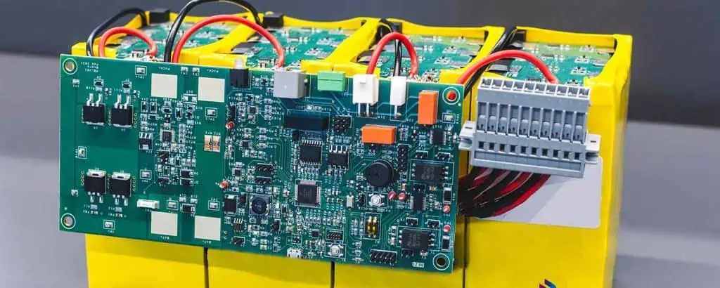
A typical PCB with electronic components mounted on it

PCBs provide a sturdy base for mounting delicate electronic components and copper tracings to route electrical signals between components. PCBs are invaluable in all electronic devices, enabling compact and reliable construction.

PCB on 18650 Battery

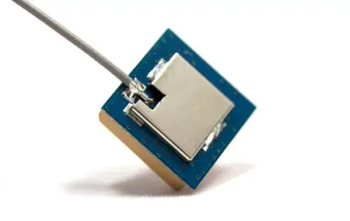
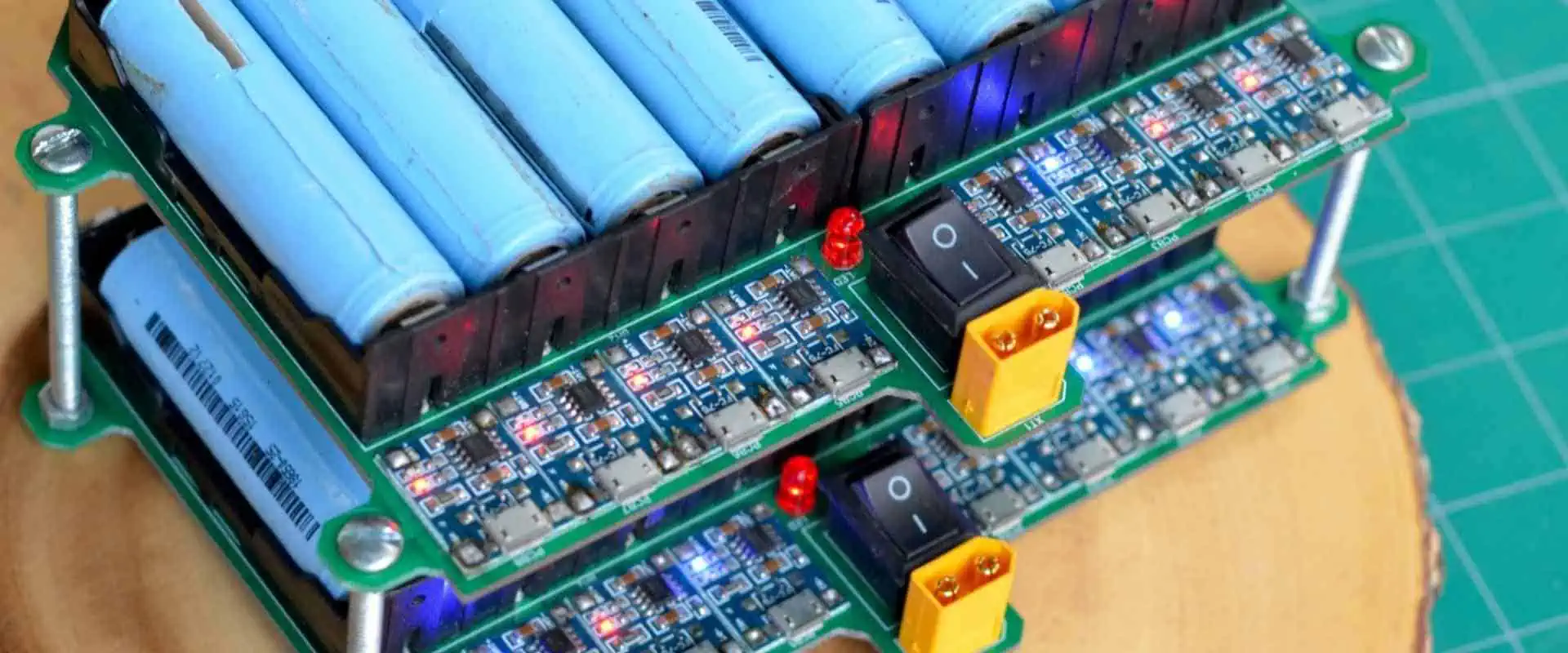
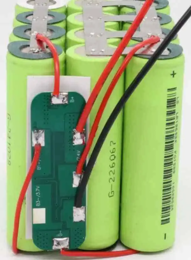
18650 battery with protection circuit module attached

The PCB on an 18650 battery, also called a protection circuit module (PCM), serves the same purpose as a PCB in other electronic devices – it routes electrical connections and mounts electronic components. However, the PCM in an 18650 battery has some additional important functions:

Overcharge Protection

When charging, lithium-ion batteries must not be charged beyond their safe voltage range, which is typically 4.2V for most 18650 cells. The PCM contains an overvoltage protection circuit that monitors the battery voltage and disconnects the battery from the charger if the voltage exceeds the safe limit. This prevents the battery from being damaged by overcharging.

Overdischarge Protection

When discharging, lithium-ion batteries must not be drained below a certain voltage threshold, around 2.5-3V for most 18650 cells. The PCM contains an undervoltage protection circuit that monitors the battery voltage and disconnects the load if the voltage drops too low. This prevents the battery from being damaged by over-discharging.

Short Circuit Protection

Short circuits can draw huge currents and overheat batteries. The PCM contains current limiting circuitry such as fuses and PTC thermistors that cut off the current if a short circuit is detected. This protects the battery from excessive current.

Cell Balancing

In multi-cell battery packs, the cells can become imbalanced over time – one cell can become overcharged/overdischarged compared to the other cells. The PCM contains cell balancing circuits that keep the cells at equal voltage and charge levels for optimal performance and life.

Terminals

The positive and negative battery terminals are connected to the PCM, which routes the current in and out of the battery. So the PCM provides easily accessible battery terminals for devices to connect to.

Protection Circuit Components

The protection circuits on the PCM are created with various electronic components that perform specific functions:

MOSFETs

MOSFET symbol

MOSFETs (Metal-Oxide Semiconductor Field Effect Transistors) are used as electronic switches to turn current flow on and off. They act as control valves that open and close based on voltages applied to their pins. In the PCM, MOSFETs turn off the connection to the battery when protection circuits detect abnormal voltages or currents.

Resistors

Resistor symbol

Resistors limit and control the amount of current flowing in a circuit. They are used extensively in protection circuits to shape response times and sensitivity to voltage/current levels. Typical resistor values in PCMs range from 1 ohm to 1 megaohm.

Capacitors

Capacitor symbol

Capacitors are energy storage devices used to smooth out voltage spikes and ripples. They help filter noise from measurements and control response rate of protection circuits. PCMs use ceramic, tantalum and electrolytic capacitors in the ranges of nano-Farads to milli-Farads.

IC Chips

IC chip symbol

Integrated chips contain complex protection circuitry in a tiny footprint. Protection ICs monitor voltage, current, temperature and control charging/discharging parameters. They may also balance cell voltages in battery packs. Common ICs in PCMs include bq20z45, DW01, S-8261 series.

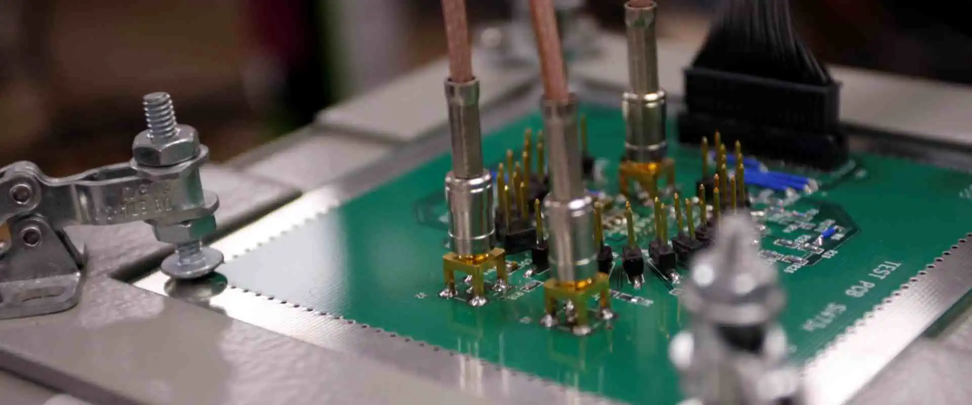
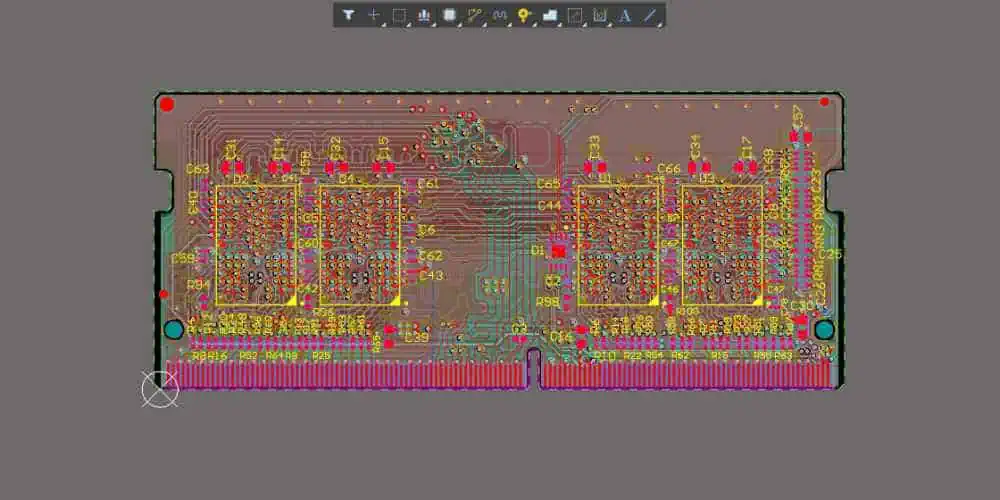
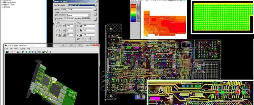
PCB Design and Construction

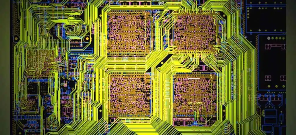
The PCB for the protection circuit is designed using CAD software that enables routing of copper traces to connect components as per the circuit diagram. The design is etched onto the PCB which is usually a double-sided or multi-layer board with copper on both sides for complex circuitry.

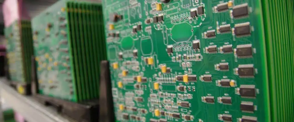
Components are precisely mounted onto the PCB using modern pick and place machines, then soldered into place. PCMs require compact designs to fit in the confined space of an 18650 battery casing. So surface mount devices are used instead of through-hole components.

The PCB fabrication uses automated processes for etching copper layers, drilling holes, applying solder mask and screen printing labels to create professional looking and functional boards. The populated PCBs then undergo functional testing before being paired with the cylindrical cell cores.

Here is a comparison of a bare 18650 cell core versus one with a PCM installed:

18650 Cell18650 Cell with PCM

The PCM gets fitted onto the cell core and makes electrical contact with the terminals. The whole assembly is then shrink wrapped with insulating material to create the finished 18650 cell.

Advantages of PCM Protection

Installing a protection circuit module onto 18650 cells has several benefits:

  • Prevents cell damage from over-charging or over-discharging
  • Protects against short circuits that can cause fires
  • Balances cells in multi-cell packs for optimal performance
  • Safety certified cells reassure end-users
  • Enables use of inexpensive core cells without native protection
  • Gives clear battery voltage indicators via protection IC communications

This allows lower cost unprotected cell cores to be transformed into safer and smarter batteries for diverse applications. The minor added cost of the PCM results in greatly improved battery performance, safety and life.

Unprotected cells should never be used standalone in devices or battery packs. The investment into a protection circuit is worthwhile for the immense dividends in battery longevity and risk reduction.

Protection Circuit Limitations

While PCMs provide invaluable protection, they do have some limitations:

  • The protection circuits consume a small amount of standby current which gradually drains the battery. The battery will still slowly self-discharge even when turned off.
  • Voltage and current thresholds have some tolerance so there is a gap between detection and complete disconnect. Some marginal over-charging or over-discharging may occur.
  • The MOSFET switches and fuses have their own resistance which causes some power loss. This increases with higher currents.
  • High currents from short circuits can sometimes exceed the speed of protection circuit response. Brief high currents may flow before being cut off.
  • Excessive ambient temperatures can prevent circuits from operating properly. Thermal overload can lead to failure.

So PCM protection should not be considered foolproof. Batteries should not be discharged below recommended cutoffs or charged beyond maximum levels. Short circuits should still be avoided. And proper heat dissipation is still necessary in battery pack design. The PCM just provides a crucial additional layer of safety.

Protection Circuit Testing

Since the PCM is so vital for battery safety, all reputable battery manufacturers perform extensive testing to ensure the protection circuits work as intended. Here are some common tests conducted:

Overcharge Protection Verification

Batteries are charged to progressively higher voltages to ensure overcharge protection activates within the specified range and prevents further charging. This confirms the upper cutoff voltage limit.

Overdischarge Protection Verification

Batteries are discharged through fixed loads down to progressively lower voltages to ensure overdischarge protection activates within the specified range. This confirms the lower cutoff voltage limit.

Short Circuit Test

A dead short is applied across the battery terminals and the resulting peak current and disconnect time are measured. This verifies the PCM can withstand and protect from short circuits.

Charge/Discharge Cycling

Batteries undergo repeated charge/discharge cycles while monitoring voltages, currents and temperatures. This evaluates protection performance over time as the battery ages.

Drop/Shock/Vibration

Physical drop tests, shock tests and vibration tests are performed to ensure PCM integrity is maintained after impacts or shaking.

Extensive testing over diverse operating conditions ensures the PCM provides robust protection throughout the battery’s service life. Independent lab certification is the gold standard for safety-critical lithium-ion batteries.

Common Protection ICs

There are a variety of integrated circuits designed specifically for lithium battery protection. Here are some of the most popular ICs used on 18650 PCMs:

Seiko S-8261 Series

The S-8261A, S-8261AB, and S-8261BA are widely used single cell lithium battery protection ICs from Seiko. They provide overcharge, overdischarge and overcurrent protection. Newer versions add cell balancing and temperature protection.

Texas Instruments BQ20z45 Series

The bq20z45 and bq2046 ICs integrate battery management and protection in a single chip. They allow communication with a host controller over an I2C interface. This enables fuel gauging and optimization of charging/discharging parameters.

Analog Devices ADP5052/5053

The ADP5052 and ADP5053 offer low power consumption single cell protection. They have undervoltage, overvoltage, and current limit protection. Thermal regulation protects during high temperature fault conditions.

Mini-Circuits ZXCT1009F

The ZXCT1009 provides simple and compact overvoltage and undervoltage protection in a tiny SC70-6 package. It consumes just 1.2ฮผA supply current making it suitable for low power applications.

DW01-P/CF/DF

The DW01 range of lithium battery protection ICs from DOWN Stream Technologies offer full protection features and safe battery state monitoring through a simple UART interface.

Conclusion

In summary, the PCB or protection circuit module on an 18650 lithium-ion battery plays a crucial role in:

  • Preventing damage from over-charge/over-discharge
  • Protecting against short circuits
  • Monitoring cell state
  • Providing easy battery connections

It allows unprotected cell cores to be turned into smart, safe batteries. The protection electronics guard against the risks of lithium-ion batteries whilst allowing them to provide high energy density storage.

Carefully designed PCMs with quality components from reputable brands help ensure the protection reliability needed in lithium battery packs. Extensive testing and safety certification provides confidence in PCM performance over thousands of charge cycles.

So next time you use an 18650 lithium-ion battery, appreciate the importance of that little PCB inside to its safe and effective operation. The PCM makes high power portable applications viable and provides peace of mind to users.

FAQs

What are the key functions of the PCM?

The main functions of the PCM are:

  • Overcharge protection to prevent over-charging above 4.2V
  • Overdischarge protection to prevent over-discharging below 2.5-3V
  • Short circuit protection via fuses and current monitoring
  • Cell balancing in multi-cell packs
  • Providing connection points for battery terminals

Does every 18650 battery have a PCB?

The vast majority of 18650 cells will have a PCB installed, but there are some “raw” unprotected cells without PCMs. These should not be used without an external PCM for safety. Protected cells with onboard PCMs are recommended.

Where is the PCM located on an 18650?

The PCM is located on the bottom end of an 18650 cell, connected between the positive and negative terminals. The protection IC and other components are on the flat surface of the PCM board.

Can an 18650 work without a PCM?

Bare 18650 cell cores will function without a PCM but have risks. There is potential for over-charge, over-discharge, short circuits and cell imbalance in packs. For reliable and safe operation, a PCM is highly recommended.

Is the PCM replaceable if damaged?

Generally no, the PCM on most 18650 cells is factory fitted and not designed to be replaced. If the PCM is damaged, the entire cell/pack should be replaced for safety. Trying to replace the PCM carries risks of short circuits.

Does a PCM reduce the battery capacity?

The PCM does use a tiny amount of power itself, so it causes a minor reduction in usable capacity. But this is small (under 5%) compared to the huge benefits in battery protection and enhanced safety it provides.

What Is The Reliability Test in PCB ?

Printed circuit boards (PCBs) must withstand years of service in demanding operating environments, from consumer devices to automotive, aerospace, medical and industrial applications. Validating PCB reliability requires testing samples under accelerated stress conditions across temperature, vibration, humidity, mechanical shock, and power cycling.

This article explores common PCB reliability tests, failure modes revealed, and how test results validate design margin and process quality. Weโ€™ll examine test methodologies, challenges interpreting results, qualifications standards, and how reliability testing reduces field failure risks. Read on for an in-depth look at this vital aspect of proving out PCB technology before volume deployment.

Reasons for PCB Reliability Testing

Thorough reliability testing provides confidence that PCBs will survive expected conditions over target lifespan requirements. Key drivers for reliability testing include:

  • Risk reduction โ€“ Identify and correct flaws before volume production
  • Process validation โ€“ Quantify manufacturing consistency and quality
  • Material selection โ€“ Prove out substrate, bonding, and coating materials
  • Design verification โ€“ Validate robustness of board stackup, layout, components
  • Qualification โ€“ Certify boards meet applicable standards like IPC or military specs
  • Improvement โ€“ Feedback to enhance design rules, processes, and QC

By stressing PCB samples beyond normal use environments, latent weaknesses are revealed enabling corrective actions. This prevents field failures and costly recalls.

PCB Failure Mechanisms and Fault Models

To develop effective reliability tests, the potential failure mechanisms in PCBs must be considered:

Electrical Shorts

  • Conductive debris creating short circuits
  • Electrical clearance inadequate under bias/humidity
  • Dendrite formation on closely spaced conductors

Open Conductors

  • Copper traces cracked by thermal cycling or shock
  • Solder joint fractures from vibration or fatigue
  • Contact pad lift or delamination

Intermittent Contacts

  • Vibration causes temporary loss of contact
  • Fretting corrosion and oxidation increases contact resistance

Dielectric Breakdown

  • Electrical arcing under high voltage bias and moisture

Cracking/Fracture

  • Thermal expansion mismatch causes component fracture
  • Vibration or shock cracks PCB substrate or joints

Corrosion/Dendrites

  • Environmental chemicals induce electrical leakage
  • Electrochemical migration of metal grows between conductors

Tests target replicating these fault conditions in an accelerated manner.

PCB Reliability Test Methods

Common PCB reliability tests include:

Temperature Cycling

  • Cycles board between hot and cold extremes
  • Assesses thermal expansion stresses and cracking
  • Standard cycles: -55ยฐC to 125ยฐC

Power Cycling

  • Power boards on and off repeatedly
  • Evaluates stresses from thermal transients
  • Checks for intermittent contacts or cracks

Vibration

  • Subjects PCB to vibration profiles
  • Screens for cracked solder joints and metal fatigue
  • Common test frequency range: 10-2000Hz

Mechanical Shock

  • Applies high G impulses to board
  • Shakes loose marginal solder joints
  • Tests for fractured components or traces

Humidity/Temperature/Bias (HTB)

  • Exposes PCBs to high heat, humidity, and voltage
  • Accelerates conditions promoting arcing, corrosion, electrochemical migration

Mixed Flowing Gas (MFG)

  • Flows mixed gas over powered boards
  • Accelerates surface corrosion and metal migration

Test standards define profiles tailored to replicate use conditions and accelerate anticipated failure mechanisms.

Interpreting PCB Reliability Testing Results

RFT Testing

The main results obtained from reliability testing are:

Pass/Fail Data

  • Were samples functional after testing?
  • Used to validate passing qualification requirements

Parametric Drift Data

  • Change in electrical parameters like resistance and capacitance
  • Gives insight into level of degradation or intermittent issues

Failure Analysis

  • Inspect failed samples to determine root cause
  • SEM, thermal imaging, bench probing used

Bathtub Curve

  • Plotting cumulative failures over test duration or cycles
  • Indicates failure rates and susceptibilities

The goal is not necessarily zero failures but rather validating design margin exists for minimal field failure rates. Extensive results enable feedback to improve manufacturing processes, design rules, components, materials and modeling.

Industry Reliability Qualification Standards

Many reliability standards exist covering various aspects of electronics:

IPC Standards

  • IPC-SM-785 โ€“ Guidelines for accelerated reliability testing of surface mount solder attachments
  • IPC-9701 โ€“ Performance test methods and qualification requirements for high frequency boards

JEDEC Standards

  • JESD22 โ€“ Extensive reliability test methods for electronics components and boards

Telcordia GR Standards

  • Telcordia GR-63-CORE โ€“ Network equipment reliability assurance
  • Telcordia GR-1221-CORE โ€“ Electrostatic discharge tolerance

MIL-STD Standards

  • MIL-STD-202 โ€“ Environmental stress testing methods for electronics
  • MIL-PRF-31032 โ€“ Certification requirements for high reliability PCBs

IEC Standards

  • IEC 60068 โ€“ Environmental testing of electronics across vibration, shock, temperature, humidity and more

Qualifying for these established standards validates achieving baseline reliability benchmarks needed for commercial and industrial applications.

Building in Design Margin

fct test

Aside from process controls, the PCB design can incorporate margin to enhance reliability:

  • Derating โ€“ Reduce voltage, current, and power limits to levels below maximums
  • Redundancy โ€“ Include backup circuits or pathways
  • Guard Banding โ€“ Provide spacing margins in layout – increase creepage, clearance
  • Simulation โ€“ Use accelerated models that consider aging effects
  • Sizing โ€“ Right-size traces, pads, and components for stresses
  • Materials โ€“ Select robust substrate materials and protective coatings
  • Diversification โ€“ Use component families with alternate internal construction
  • Monitoring โ€“ Built-in sensors to monitor temperature, vibration, etc.
  • Quality Components โ€“ Select reputable suppliers and proven parts

Building in margin provides insurance should unanticipated overload or use conditions emerge. This avoids โ€œjust good enoughโ€ designs prone to field failures.

Incorporating Reliability Testing in PCB Development

A strategic approach to reliability testing balances risk reduction with development costs:

Material and Component Testing โ€“ Start reliability testing at the material level before full PCB design to validate robustness.

HALT/HASS โ€“ Highly Accelerated Life Testing reveals failure points through extreme stressing.

FMEA โ€“ Failure Mode and Effects Analysis predicts risk areas to guide qualification.

Early Prototypes โ€“ Test initial prototypes under accelerated conditions to guide design revisions.

Process Validation โ€“ Apply reliability tests for new technologies before volume ramp.

Qualification Testing โ€“ Certify boards meet requirements as part of architecture freeze.

Ongoing Monitoring โ€“ Continue testing during volume production for process control and outlier detection.

Regression Testing โ€“ Validate reliability when revising designs or upgrading manufacturing lines.

Reliability cannot be an afterthought but must factor in throughout the PCB development, qualification, and production lifecycle.

Conclusion

Rigorously testing PCBs under accelerated stress conditions reveals design flaws and manufacturing defects before volume deployment. While passing established reliability qualifications provides a baseline level of confidence, continuous failure analysis and process improvements are needed to meet modern demands for service life spanning decades in challenging operating environments.

By incorporating reliability engineering principles spanning design, materials selection, modeling, testing, inspection, and continuous feedback, electronics producers can deliver robust PCB products with minimized risks of field failures. The result is dependable electronics underpinning safety-critical infrastructure across end-markets from automotive to medical to aerospace applications.

Frequently Asked Questions

What is the typical sample size used for qualification testing?

Sample sizes vary based on program criticality. High volume consumer devices may use 3-5 samples. High reliability military boards may test 25+ samples per lot. Setting sample criteria depends on risk analysis and desired statistical confidence.

How should I interpret intermittent faults during testing?

Intermittent failures often point to marginal design margin, manufacturing variances, or component inconsistencies. Any tendency for intermittent operation under stress should be investigated through root cause analysis, as it may indicate susceptibility to field failure.

What is an appropriate length of time for power or temperature cycling testing?

There is no set rule. Choosing numbers of cycles and test duration involves tradeoffs between risk reduction, development time, and cost. Hundreds to thousands of cycles spanning days to weeks of continuous testing is typical.

Should every PCB design go through rigorous qualification testing?

It depends on production volume and end use environment. High volume consumer goods and safety-critical boards should undergo extensive qualification. Low volume lab equipment may rely more on design margin.

How are results from accelerated testing correlated to real world conditions?

Careful analysis is required using acceleration factors and reliability models. But uncertainties remain, so it is recommended to test with greater than actual severity and duration to provide engineering margin.

What Are Nets on PCB?

In printed circuit board (PCB) design, the term “net” refers to electrical nodes or points that need to be connected together in the circuit layout. Nets represent the logical connectivity defined in the schematics. All pins and ports that are connected together electrically belong to the same net.

PCB layout involves identifying all nets and then connecting them on the board layout using copper traces and vias while meeting design rules. Understanding the role of nets is key for successful board layout and manufacturing. This article provides an in-depth overview of PCB nets – what they are, how they are specified, routing considerations, and more.

What is a Net in PCB Layout?

A net is defined as a collection of electrically connected nodes or points which need to be joined with copper tracking to make them a single signal or potential point. Some key points:

  • Nets represent logical rather than physical connections.
  • All component pins part of a net must be at same electrical potential.
  • A net may have 2 or more component pins/pads connected to it.
  • Multi-point connections define nets – e.g. common power or ground nets.
  • Nets get mapped to physical PCB copper tracking during layout.
  • Each net is identified by a unique name or number.

Essentially, nets list which pins and ports on the schematic are meant to be connected electrically on the PCB layout. Correct netlist definition is crucial.

Example of multiple PCB component pins belonging to a common net

Why Specify Nets in PCB Layout?

Defining nets serves several important purposes:

  • Captures logical connectivity – Nets represent schematic connectivity requirements that must be achieved with physical layout.
  • Enables ERC – Electrical rules checking verifies all nets are properly connected with no opens or shorts.
  • Facilitates autorouting – Routers can use net info to automatically connect defined nets.
  • Allows design validation – Netlist can be cross-checked against schematics for correctness.
  • Aids manufacturability – Unconnected nets highlight problems for assembly and test.
  • Speeds fault isolation – Confirms if bad joints/breaks are causing net opens.

In summary, identifying nets is key to translating the electrical connectivity model into the physical PCB layout correctly while meeting design rules.

Specifying Nets in CAD Tools

PCB layout CAD tools like Altium Designer provide powerful support for defining, managing and routing nets spanning multiple component pins. Some key features related to nets:

Net Identifier

A unique name or number assigned to each net. Can be auto-generated or user-defined. Examples: NetA, Power, +5V, Audio_Out etc.

Net Scope

The logical boundary or extent of a net. Allows optimization of routing boundaries.

Net Classes

Nets can be grouped into classes with shared rules like routing widths, spacing, via styles etc.

Net Tie

An electrical connection defined between two different nets that forces them to be shorted.

Power Planes

Entire plane layers can define nets like GND or VCC, allowing connections through vias.

Differential Pairs

Grouping differential signal nets enables linked length-matching routing.

Net Properties

Nets can have attributes like drive current, impedance, delay etc. attached for analysis.

Proper specification of these net parameters in the PCB CAD system is needed for robust ERC checks, autorouting and design validation against schematics.

Guidelines for Naming Nets

When defining custom net names, following naming conventions helps keep netlists well-organized and easy to understand:

  • Keep names short but meaningful e.g. “PWREN” instead of “POWERENABLE”.
  • Use consistent prefixes for net types e.g. “SIG_” for signals, “PWR_” for power.
  • Avoid using non-alphanumeric characters in names to prevent tool issues.
  • Use uppercase letters to make names stand out.
  • Include pin numbers if needed for clarity e.g. “CLK2”
  • Use sequential numbers for grouped nets e.g. “D0-D7”.
  • Add relevant functional descriptions e.g. “LED_STATUS”
  • Designate I/O signals clearly e.g. “USB_D+”

Intelligent net naming strategies help identify the signal or connection purpose at a glance during layout routing and inspection.

Cross-Probing to Schematics

Modern PCB CAD tools allow cross-probing from PCB layout to schematics to quickly understand net connectivity and context. When clicking a net in layout, the associated pins/nodes in the schematics are automatically highlighted.

Visual cross-probing from PCB layout net to schematic net highlights associated pins

This very useful feature allows layout designers to instantly visualize which component pins belong to a net. It aids in layout decisions like optimal component placement and routing paths to maintain net integrity.

Routing Considerations for Nets

When laying out nets using copper tracks and vias, several factors must be considered:

  • Priority – Route critical nets like clocks and power first.
  • Topology – Use point-to-point, daisy chains or tree routing as appropriate.
  • Impedance – Match trace geometry to required impedance.
  • Currents – Size tracks based on expected current.
  • Length Matching – Equal net lengths for clocks, differential signals etc.
  • Crosstalk – Provide adequate spacing between nets.
  • Stackup – Use correct signal layers.
  • Shielding – Shield noisy traces using ground planes.
  • Terminations – Add resistors at line ends when needed.
  • Vias – Minimize/avoid vias on critical nets.

Applying these rules during layout ensures nets get implemented with the desired signal quality and integrity.

Best Practices for Defining Nets

Follow these guidelines when specifying nets for a PCB layout:

  • Capture all component-to-component connections as nets – avoid assuming implied connections.
  • Group multiple pins of IC/connectors into nets representing bussed signals.
  • Review the netlist against schematics and datasheets thoroughly to prevent omissions.
  • Define power and ground nets carefully for power integrity analysis.
  • Use named nets rather than direct component-to-component connections for clarity.
  • Re-use common nets rather than defining duplicates to minimize errors.
  • Create differential pair and bus nets to simplify routing and constraints.
  • Specify net classes and routing rules based on signal types – clock, data, analog etc.

Well-defined nets are crucial for achieving smooth PCB layout implementation and avoiding manufacturing issues due to incorrect copper connectivity.

Conclusion

In summary, PCB nets provide the vital link between the logical connectivity in an electrical schematic and the physical layout topology on the board. Defining nets correctly and routing them according to electrical and layout constraints is key to creating fabrication-ready PCB artwork. CAD systems simplify net handling with features like auto-naming, cross-probing, classes and differential pairs. With the growth in design complexity, net management has become critical for layout success. Understanding every aspect of PCB nets is essential for both design engineers and layout specialists.

FAQ

Here are some common questions about nets in PCB layout:

Q1: Can two nets have the same name in a PCB layout?

No, each defined net must have a unique name to avoid ambiguity during layout. Identical names would lead to connection errors.

Q2: How are net names transferred from schematic capture to PCB layout?

The netlist, which maps net names to component pins, is passed from schematics to PCB layout either as a file or through direct tool integration.

Q3: Can net scope constrain routing to a particular PCB region?

Yes, the scope can define a keep-in or keep-out region for a net’s routing to optimize layout.

Q4: What is a net tie?

A net tie intentionally shorts two nets together by defining a connection between them. It is useful for tying power/ground nets.

Q5: Can simulation use the netlist from PCB layout?

Yes, the layout netlist can be used for signal integrity and power integrity analyses using simulators.

UNDERSTANDING THE DESIGN AND MANUFACTURE OF ELECTRIC VEHICLES

Electric vehicles (EVs) are automobiles powered entirely or significantly by electricity. Unlike conventional vehicles that rely solely on internal combustion engines, EVs use electric motors and motor controllers for propulsion. This provides quieter, smoother operation and substantially reduced air pollution compared to gasoline-powered vehicles.

Below we examine the key components and systems involved in EV design and manufacturing that enable sustainable personal transportation.

Drivetrain Design

The drivetrain provides power to the wheels for propulsion. A typical EV drivetrain consists of:

  • Traction batteries – Provide electrical energy storage
  • Electric motor – Converts stored electricity into mechanical power
  • Power electronics – Controls motor operation
  • Transmission – Transfers torque to wheels
  • Wheels/axles – Deliver driving force to road

Traction Batteries

Rechargeable lithium-ion batteries are predominantly used:

  • High energy and power density
  • High cycle life
  • Reasonable cost
  • Require sophisticated battery management system (BMS)

Battery packs contain many cells connected in series and parallel to deliver high voltage (200 to 400V) and capacity (50 to 100+ kWh). The large battery capacity provides an EV’s driving range on each charge.

Electric Motors

Permanent magnet AC synchronous and induction motors are common choices due to their high efficiency and performance:

  • Compact and lightweight
  • High torque capability for acceleration
  • Operate at over 90% efficiency

Motors are typically in the 50 to 150 kW continuous power range, using high density magnets and advanced control algorithms. Some EVs use multiple motors for all-wheel drive capabilities or independent torque control.

Power Electronics

Power electronic inverters and converters provide precise motor control:

  • Convert DC battery output to adjustable AC for motor
  • Allows torque and speed regulation through pulse width modulation
  • Facilitates regenerative braking for energy recovery

The power electronics strongly influence overall drivetrain efficiency.

Transmission

A single speed gear reduction transmission is typically used:

  • Maximizes efficiency by avoiding losses in a multi-gear transmission
  • Simpler, more reliable, and lower cost
  • Electric motor provides wide torque/speed range needed for desired performance

Some EVs use a 2-speed transmission for improved highway range and efficiency.

Vehicle Design Optimization

EVs are designed for maximum range, performance, safety and efficiency:

Lightweighting

  • Use of lightweight materials like aluminum and carbon fiber reduces mass
  • Lower mass requires less energy to accelerate and climb hills

Aerodynamics

  • Streamlined body shapes minimize air resistance
  • Improves highway range where air drag is dominant

Regenerative Braking

  • Kinetic energy during braking is recovered as electricity
  • Stores energy in battery rather than wasting it as heat

Thermal Management

  • Liquid heating and cooling loops optimize temperatures for batteries, motors, and power electronics

Low Rolling Resistance Tires

  • Tires specifically engineered to minimize road friction
  • Reduce energy lost deforming tires while driving

Careful attention to these factors maximizes the vehicle’s driving range per battery charge.

EV Manufacturing

Producing EVs involves some unique processes:

Battery Module/Pack Assembly

  • Individual cells closely packed together into modules
  • Modules assembled and interconnected into a full battery pack
  • Enclosure integrates cooling plates, monitoring electronics, and safety features

Powertrain Integration

  • Electric motor(s), gearbox, inverter, charger, converter, etc. assembled into a modular powertrain system
  • Simplifies manufacturing by integrating components together early

Alignment of Chassis and Powertrain

  • Motor and gearboxes aligned precisely to axles and wheels
  • Eliminates driveline vibrations and noise

Lightweighting Processes

  • Extensive use of aluminum and plastics instead of steel
  • Carbon fiber, magnesium, and other exotic materials utilized
  • Advanced joining techniques like aluminum laser welding

Battery Installation

  • Entire battery pack inserted and secured as single unit
  • Simplifies assembly compared to positioning many small cells

Testing and Validation

  • Extensive voak testing to ensure battery safety
  • Validating vehicle range and performance specifications
  • Verifying adherence to regulatory compliance

These processes aim to streamline manufacturing by designing assemblies for ease of automation, reducing part counts, and utilizing techniques tailored for EV architectures.

Battery Technology Innovations

Developing better batteries is central to making affordable, long range EVs. Key areas of battery research:

Cell Chemistries

  • Alternative anodes like lithium titanium oxide (LTO)
  • Advanced cathodes like lithium nickel manganese cobalt oxide (NMC)
  • Solid state electrolytes to replace liquid electrolytes
  • Lithium sulfur and lithium air as potential high energy chemistries

Active Materials

  • Silicon composite anodes for higher energy density
  • Nickel-rich cathodes to reduce cobalt content
  • Nanomaterials to shorten lithium ion diffusion pathways

Cell Design

  • Tabless electrodes to improve thermal performance
  • Dry electrode coating processes to increase energy density
  • Three-dimensional electrode architectures

Manufacturing Improvements

  • Wet coating processes for thicker, more uniform electrodes
  • Advanced drying techniques like freeze drying
  • Roll-to-roll production for higher volumes

These innovations aim to improve battery energy density, power, durability, safety, production volume, and cost – all factors critical to widespread EV adoption.

Charging Infrastructure Growth

Convenient public and home charging options are essential to make EVs practical:

Home Charging

  • Faster Level 2 chargers (6-20 kW) reduce charge times
  • Smart charging coordinates with grid to lower costs
  • Bidirectional charging allows V2G electricity flow

Public Charging

  • DC fast chargers (50-350 kW) enable long distance travel
  • Workplace charging expands opportunities

Grid Integration

  • Easy payment methods via apps, cards, automatic billing
  • Universal connectors and charging standards
  • Improved reliability and uptime

Widespread charging availability addresses range anxiety and improves EV satisfaction.

Emerging Trends

Electric Vehicle Based on Battery Charging Fuel Independent
  • Declining battery prices will reach $100/kWh threshold enabling cost parity with gas vehicles
  • Faster charging rates will minimize charging times to add hundreds of miles quickly
  • New learning-based battery management systems will extend range and lifetime
  • Simplified drivetrain architectures will reduce manufacturing costs
  • Enhanced vehicle-grid coordination will make EVs valuable grid assets

These trends will drive continued EV adoption and improvement.

Frequently Asked Questions

  1. What are the main components in an electric vehicle drivetrain?

The key components are the traction batteries, electric motor(s), power electronics, transmission, and wheels/axles.

  1. How do manufacturers optimize EVs for maximum range?

Range is extended through lightweighting, aerodynamics, regenerative braking, thermal management, and low rolling resistance tires.

  1. What manufacturing processes are unique to EVs?

Key EV manufacturing processes include battery assembly, powertrain integration, precision motor-wheel alignment, lightweight material fabrication, and battery installation.

  1. What battery innovations are being worked on for EVs?

Important areas of battery research are new chemistries, advanced active materials, innovative cell designs, and improved manufacturing processes.

  1. Why is public charging infrastructure so important for EVs?

Convenient and plentiful public charging enables long distance travel and assures drivers they can charge when needed, reducing range anxiety.

What is RF Antenna? Definition, Design, Types, & Uses

5G Microstrip Antenna

An RF antenna is a device used to transmit and receive radio frequency signals. Antennas couple electromagnetic waves between free space and electronic transmitting or receiving circuitry. They provide the air interface for wireless communications, broadcasting, radar and other applications.

Below we examine how antennas work, key design parameters, different antenna types, characteristics, and typical applications where antennas are essential components.

RF Antenna Definition

An antenna is a specialized transducer that converts signals from an electronic transmission line to electromagnetic waves that propagate through space, and vice versa. Antennas couple energy between a guided wave in a conductor and an unguided electromagnetic wave in free space.

Key properties of an ideal antenna:

  • Efficiently radiates electromagnetic energy into space
  • Effectively intercepts and collects electromagnetic waves
  • Matches the characteristic impedance of connected circuitry
  • Exhibits resonant operation at the desired frequencies
  • Omnidirectional or unidirectional radiation patterns when needed
  • Rugged, resistant to environmental conditions like weather
  • Compact size while still providing adequate gain and bandwidth

In transmitting mode, an antenna converts the low voltage, high current signal from a transmission line into an electromagnetic field that detaches from the antenna and propagates through space as a radio wave.

In receiving mode, electromagnetic waves induce a voltage across the antenna, generating a small radio frequency current that is applied to the electronic receiver circuitry.

How Antennas Work

An antenna’s operation depends on the time-varying electric or magnetic fields produced by an alternating current flow through the antenna. This alternating current is generated by the connected transmitter or induced into the antenna by intercepted radio waves.

The oscillating electric and magnetic fields produced by the antenna create propagating electromagnetic waves. The nature of the fields and resulting radiation depends on the antenna geometry, driving frequency, and surrounding environment.

An antenna designed for a particular application optimizes this transformation between guided waves and free space waves. Efficiency, directionality, bandwidth, polarization and other factors are tailored for the radio link requirements.

Antenna Key Parameters & Characteristics

Below are some of the key parameters and figures of merit used to evaluate antenna performance:

  • Gain – Measure of antenna concentration of radiated power in a particular direction.
  • Directivity – Directionality of the antenna’s radiation pattern.
  • Radiation pattern – 3D spatial distribution of the antenna radiated power.
  • Bandwidth – Range of frequencies over which antenna performance is acceptable.
  • VSWR – Voltage standing wave ratio, metric of the impedance match to transmission line.
  • Return loss – Loss of signal returning/reflecting from the antenna due to mismatch.
  • Input impedance – Antenna impedance at the feed terminals or input port.
  • Efficiency – Ratio of radiated power to input power.
  • Polarization – Orientation of the antenna electric field.
  • Beamwidth – Angular width measured between half power (-3 dB) points of main lobe.

These parameters guide the process of designing and evaluating antennas for particular RF applications.

Types of Antennas

Many different antenna types and geometries exist, each with unique properties making them suitable for certain applications. Broad classifications of antennas include:

  • Omnidirectional antennas – Radiate power uniformly in all directions in a single plane. Common types are dipole and monopole.
  • Directional antennas – Focus radiation and reception in specific directions. Common types are patch, parabolic, and Yagi-Uda.
  • Aperture antennas – Open structures utilizing an aperture to enhance radiation over a large area. Common types are horn and reflector.

Antennas also employ a wide variety of feeding techniques to couple signals to/from transmission lines:

  • Direct feed – Coaxial cable attached directly to antenna.
  • Capacitive or inductive coupling – Using reactive coupling between feed line and antenna.
  • Aperture coupling – Feeding through a small slot or aperture.

Below we look at some of the most common and important types of antennas:

Wire Antennas

Wire antennas are constructed from thin metal wires usually arranged linearly or in loops. They are simple, inexpensive to construct, and lightweight.

Monopole – Single straight wire antenna with ground plane. Omnidirectional radiation pattern. Quarter-wave monopoles are most common.

Dipole – Two straight collinear wires connected centrally. Balanced structure with omnidirectional pattern. Half-wave dipoles are most common.

Loop – Wire loop or coil with maximum radiation perpendicular to the plane of the loop.

Common wire antenna configurations

Wire antennas are widely used in communications, broadcasting, instrumentation, radar and other applications. Their simplicity and omnidirectional characteristics make them suitable for many purposes.

Aperture Antennas

Aperture antennas utilize an open physical area to enhance radiation. The larger the aperture area compared to wavelength, the greater the gain and directionality.

Horn – Flared metal waveguide shaped like a horn to match wave impedance of space. Very high gain, narrow beamwidth, and broadband frequency capability.

Reflector – A dish or mirror reflecting radio waves from a primary feed antenna. Shaped to produce a directional beam for high gain performance. Used for radar, satellite, and deep space communications.

Slot – Narrow aperture cut into a metal screen. Feedline behind screen crosses aperture transversely, emitting radiation on other side.

Aperture antennas with exposed physical area to enhance radiation

Aperture antennas produce very high gain, directionality, and power handling for long range applications. The parabolic reflector is the classic high gain directional antenna.

Microstrip Patch Antennas

Microstrip or patch antennas are fabricated using printed circuit board technology. They offer low-profile planar structures ideal for aerospace, mobile, and compact applications.

Patch – Square or rectangular conductive patch on top of PCB substrate, fed by a microstrip line below. Radiates perpendicular to the patch. Moderate to high gain with directional beam.

Planar inverted-F – Miniaturized patch antenna shorted on one edge using printed transmission line trace. Requires ground plane below substrate. Omnidirectional to directional patterns.

Low profile microstrip and patch antennas

Microstrip antennas allow antennas to be fabricated cost effectively as part of the electronic circuit PCB. Their compact size facilitates use in mobile and handheld wireless devices.

Array Antennas

Connecting multiple individual antenna elements together into an array provides greater control over directionality and gain:

  • Elements spaced apart at fraction of wavelength
  • Fed with equal amplitude and phase for broadside radiation
  • Corporate feed or space feed used to control pattern
  • Permits shaping of beamwidth, sidelobes, and gain

Arrays can scan electronically by shifting phase to elements or mechanically by moving entire array.

Antenna arrays combining multiple individual elements

Arraying antennas offers tremendous versatility in designing complex antenna performance characteristics.

Antenna Characteristics

Below we examine some of the key parameters and figures of merit used when designing, analyzing, and evaluating radio frequency antennas.

Radiation Pattern

The radiation pattern describes the spatial variation in radiated power density from the antenna across different directions in 3D space. Usually represented graphically in polar or rectangular plots:

3D and 2D polar plot radiation pattern of directional antenna

Analysis of the main beam lobe, sidelobes, backlobes and nulls provides insight into antenna performance.

Directivity and Gain

Directivity compares an antenna’s radiated power density in its direction of maximum radiation versus the power density from an isotropic radiator (point source).

Gain describes how much power is transmitted in the peak direction compared to the power supplied to the antenna terminals.

Gain and directivity differ by the antenna efficiency factor. Higher gain concentrates radiated power into a smaller spatial angle.

Input Impedance

Input impedance Z<sub>in</sub> is the impedance presented by the antenna at its terminals. This determines the impedance match to the connected transmission line for efficient power transfer and low reflections.

50 ohm or 75 ohm matching are common. Matching networks may adapt other impedances.

Voltage Standing Wave Ratio (VSWR)

VSWR measures the impedance mismatch between transmission line and antenna. It is the ratio of the voltage maxima to minima along the feed line. Lower VSWR values represent better antenna matching:

VSWR describes the voltage standing wave pattern caused by impedance mismatches

Typical specifications require VSWR less than 2:1 or 3:1 over the operating bandwidth.

Bandwidth

Antenna bandwidth is the range of frequencies over which performance meets specifications. Impedance match, gain, radiation pattern, polarization, and efficiency should remain within acceptable limits across the entire bandwidth.

Narrowband antennas may operate over fractions of a percent while ultrawideband antennas may achieve decades of bandwidth.

Beamwidth

Beamwidth measures angular width of the main radiation lobe, usually defined using half-power (-3 dB) points:

Beamwidth quantified using -3 dB angle off peak radiation

Narrow beamwidth concentrates radiation for high antenna directivity and gain.

Polarization

Polarization describes the orientation of the electric field component of the radio wave. Key polarizations:

  • Linear – Electric field fixed along one axis. Vertically or horizontally polarized.
  • Circular – Electric field rotates clockwise or counterclockwise with propagation. Used in satellite communications.
  • Elliptical – Electric field rotates elliptically in the plane perpendicular to propagation. General case of circular polarization.

Various electromagnetic wave polarization types

Polarization is an important antenna property matching receivers to transmitted waves.

Antenna Efficiency

Efficiency metrics quantify how much power delivered to the antenna is actually radiated as electromagnetic waves:

Radiation efficiency – Ratio of radiated power to total accepted power

Total efficiency – Ratio of radiated power to net input power

Losses such as I^2R heating, dielectric absorption, and impedance mismatches reduce efficiency below 100%. Highly efficient antennas minimize internal losses and maximize radiated power.

Typical Antenna Applications

Antennas enable wireless connectivity, broadcasting, sensing and observation across the radio spectrum:

  • Communications – Connecting cell phones, WiFi devices, Bluetooth headsets, emergency radios, and other electronic systems wirelessly. Antennas are embedded or external.
  • Broadcasting – Transmitting radio, television, satellite TV and mobile audio programming to individual receivers and cell sites. High gain outdoor antennas used.
  • Radio astronomy – Large specialized antennas like Arecibo and Very Long Baseline Arrays gather faint cosmic microwave signals for scientific observation.
  • Radar – Detecting objects by analyzing reflected EM waves. Directional high gain antennas required for long range radar. Used for air traffic control, meteorology, and target tracking.
  • Satellite – Parabolic dish antennas transmit and receive signals over huge distances to communicate with Earth orbiting satellites for data, video, telephony, and military uses.
  • RFID – Small antennas in UHF or microwave bands transfer data to/from RFID tags for item identification and tracking.
  • Medical – RF and microwave signals applied in body imaging techniques including MRI and diathermy therapeutic tissue heating.

These key applications demonstrate the indispensable role antennas play in any system involving transmission, reception or interaction with electromagnetic waves across the radio spectrum.

Frequently Asked Questions

  1. What is an antenna?

An antenna is a device used to transmit and receive radio frequency signals by converting electromagnetic waves in space to electrical currents and vice versa. They provide the air interface for wireless communications.

  1. What are the key properties of an antenna?

Important antenna parameters are gain, directivity, radiation pattern, impedance, bandwidth, VSWR, beamwidth, polarization and efficiency. These determine suitability for particular applications.

  1. What are the main types of antennas?

Common antenna types include wire antennas like monopoles and dipoles, aperture antennas like horns and dishes, microstrip patch antennas, and antenna arrays combining multiple elements.

  1. How does an antenna concentrate radiated power?

By focusing the emitted electromagnetic waves in a particular direction, an antenna concentrates signal power into a narrow solid angle for increased gain and directivity.

  1. What applications use antennas?

Antennas are essential components enabling technologies including communications, broadcasting, radar, radio astronomy, satellite links, RFID, medical RF, and any application involving transmission/reception of radio waves.

What Is IoT (Internet of Things)? Definition, Types, Technologies and Applications

IoT Devices

What is IoT?

IoT stands for Internet of Things. It refers to the network of physical objects embedded with sensors, processing ability, software and other technologies that connect and exchange data over the Internet or other communications networks.

IoT enables objects to be sensed and controlled remotely over the existing network infrastructure creating opportunities for direct integration of physical world into computer systems. This allows improving efficiency, accuracy and economic benefit in addition to reduced human intervention.

The IoT concept builds on the proliferation of smart devices like smartphones, tablets, sensors and connected vehicles that collect and transmit data via the internet. When objects can represent themselves digitally, they can be controlled from anywhere.

Some key aspects of the IoT include:

  • Physical objects with embedded technology to interact and communicate
  • Network connectivity to share data and remote control
  • Internet protocols, standards and architecture
  • Intelligent data analytics and algorithms

A Simple IoT Example

A simple example of an IoT system is a smart home, where devices and appliances are connected to a network and can be remotely monitored and controlled:

  • Smart thermostat automatically adjusts temperature and optimizes heating/cooling energy costs
  • Smart lighting adjusts LED brightness based on time of day and occupancy
  • Smart locks allow remote control of door locks via smartphone
  • Smart appliances communicate usage data to optimize electricity utilization
  • Security cameras provide alerts and remotely stream video
  • Smoke/CO detectors send instant alerts to phones in emergency

All these connected devices collect data, relay commands, and enable remote control through internet connectivity. IoT enables new levels of efficiency, automation and responsiveness.

IoT Definition

IoT can be defined as:

โ€œA system of interrelated computing devices, mechanical and digital machines provided with unique identifiers (UIDs) and the ability to transfer data over a network without requiring human-to-human or human-to-computer interaction.โ€

Key aspects of this definition include:

  • Computing Devices – Embedded systems with processing, memory and network connectivity. Can include edge devices or cloud servers.
  • Mechanical/Digital Machines – Smart objects with sensors, actuators and software. Allows physical world interfacing.
  • Unique Identifiers – Addressability of each object within the IoT system, like an IP address. Allows unified data coordination.
  • Data Transfer – Objects autonomously exchange data facilitating remote monitoring and control reducing human intervention.
  • Network Connectivity – Leverages existing internet infrastructure enabling connectivity.

This represents the essence of the IoT concept – enabling intelligent, interconnected ecosystems of technology to automate tasks and augment human capabilities.

RAYMING 4 Layer IoT Household air purifier PCB

RAYMING 4 Layer IoT Household air purifier PCB

Original price was: $19.00.Current price is: $18.50.

Product name: 4-layer Internet of Things PCB boards Board Material: TU-662 Thickness: 1.6mm Layer Number๏ผš4 layers PCB Minimum line width/spacing: 6/6mil Finished copper thickness: inner layer 2OZ, outer layer 2OZ Acceptance standard: IPC6012 CLASS 2 level Surface technology: lead-free HASL Dielectric constant: 4.3 Loss factor: 0.014 Usage: Household air purifier   4 Layer IoT Household…

Brief History of IoT

The Internet of Things as a concept has evolved over several decades:

  • 1970s – Early internet protocols like TCP/IP were developed enabling internetworking
  • 1990s – As more devices were connected, the term โ€œubiquitous computingโ€ was coined to describe the prevalence of computing
  • 1999 – Kevin Ashton coined the phrase โ€œInternet of Thingsโ€ to describe a system where objects in the physical world could be connected to the internet.
  • Early 2000s – RFID and wireless sensor networks emerged as enabling technologies. Focus on machine-to-machine communications.
  • 2008 – The number of connected devices exceeded the human population.IoT concept gained popularity.
  • 2009 – Number of internet connected objects surpassed the number of computers on the internet.
  • Present Day – Billions of devices now connected forming a global network. IoT continues to expand into many application domains.

We now live in a hyper-connected world with billions of devices interconnected and exchanging data. IoT has moved from concept to reality.

IoT System Architecture

A generic IoT system architecture consists of:

1. Physical Layer

Composed of embedded devices with sensors and actuators to interface with the real world. Includes smart wearables, appliances, industrial machines, vehicles, and more.

2. Network Layer

Provides connectivity and communications using protocols like WiFi, Bluetooth, LPWAN, cellular, satellite, etc. Can include gateways and routers.

3. Edge Computing Layer

Distributed intelligence in the form of real-time analytics and processing at the edge of the network rather than relying solely on the cloud. Often uses embedded systems or micro data centers.

4. Platform Layer

Central hubs that aggregate, process, analyze and disseminate data. Provides management, security and data storage. Cloud platforms or on-premise servers.

5. Application Layer

Human interaction with the IoT system using apps and visualization. Enables monitoring, remote control, analytics, dashboards, etc.

This provides a framework to understand the core technology components that enable an IoT ecosystem. Different architectures can vary based on the specific use case.

IoT Enabling Technologies

IoT devices raspberry pi

Several key technologies have converged to enable the Internet of Things:

  • Sensors – MEMS accelerometers, gyroscopes, temperature sensors, pressure sensors, etc that interface with the physical environment.
  • Actuators – Motors, servos, valves, switches and more that provide physical motion or control.
  • Smart Devices – Powerful embedded systems like microcontrollers, System on Chips, Single Board Computers that enable local processing.
  • Communication – Wireless networking technologies like WiFi, Bluetooth, LoRaWAN, NB-IoT, LTE-M and 5G provide connectivity.
  • Identification – RFID tags, barcodes, cameras enable identifying and tracking objects.
  • Location – GPS, cellular, WiFi triangulation enables location tracking capabilities.
  • Power – Battery technology, energy harvesting and wireless charging enable untethered operation.
  • Data Analytics – Analytics algorithms extract insights from sensor data streams using techniques like machine learning and AI.
  • Cloud/Fog Computing – Cloud platforms provide data aggregation, processing, visualization and storage. Fog/edge computing enables some decentralized processing.
  • Network Protocols – Networking standards like TCP/IP allow objects to communicate over the internet infrastructure.

The maturity and ubiquity of these technologies has allowed the IoT concept to move beyond hype into mainstream adoption.

IoT Connectivity Protocols and Standards

For IoT ecosystems to function efficiently, connected devices and systems need to speak a common language. A variety of protocols, network architectures and standards enable devices to communicate:

TCP/IP – Transmission Control Protocol / Internet Protocol that provides addressing scheme along with reliable transmission of data packets between internet connected devices.

6LoWPANIPv6 over Low Power Wireless Personal Area Networks. Enables IP-based communications for low power devices like sensors.

MQTT – Message Queuing Telemetry Transport lightweight publish-subscribe messaging protocol well suited for IoT devices.

AMQP – Advanced Message Queuing Protocol for queuing and routing enterprise messages between clients.

CoAP – Constrained Application Protocol, a web transfer protocol designed for low power devices.

LWM2M – Lightweight M2M protocol from OMA for managing IoT/M2M device services.

LoRaWAN – Long Range Wide Area Network protocol for low power wide area networks.

DDS – Data Distribution Service real-time middleware protocol from Object Management Group.

OPC-UA – Open Platform Communications Unified Architecture standard for industrial automation.

oneM2M – Global M2M/IoT standard that enables interoperability across multiple industries and domains.

Adherence to common protocols and standards ensures interoperability between diverse systems and allows them to exchange data.

IoT Security Challenges

With billions of connected devices, IoT systems pose unique security challenges:

  • Weak default passwords on devices
  • Lack of encryption on data communications
  • Insecure network interfaces
  • No secure hardware storage
  • Lack of physical hardening
  • Infrequent security patch updates
  • Exploitable software bugs
  • Large unmonitored attack surface

This can lead to cyberattacks against IoT networks like:

  • Botnets controlling swarms of devices
  • Leaked personal data from wearables or smart homes
  • Safety critical manipulations like vehicle brake overrides
  • Ransomware attacks that disable systems
  • Privacy violations from sensor data leaks
  • Data integrity loss from malicious data manipulation

IoT security issues can undermine consumer confidence in the technology and pose major risks to individuals and organizations. Securing IoT ecosystems remains an ongoing challenge and priority.

IoT Design Principles

5G IoT Technology

To architect effective and secure IoT systems, key principles include:

  • Simplicity – Avoid unnecessary complexity in design to minimize vulnerabilities. Use compact protocols optimized for IoT.
  • Resiliency – Build in backup mechanisms in case of outages. Assume unreliable network connectivity. Design for occasional power loss.
  • Modularity – Reusable, interoperable components and interfaces improve flexibility and maintenance. Design for piecewise updates.
  • Statelessness – Avoid retaining excessive state or session information that may be lost. Design stateless interfaces when possible.
  • Redundancy – Critical systems should have fail-over mechanisms with redundant components.
  • Heterogeneity – Design for multiple platforms, operating systems, and generations of technology.
  • Security – Consider security from the ground up rather than an afterthought. Utilize encryption, authentication, validation, monitoring and other security measures.

Adhering to these design tenets can help create robust and secure IoT ecosystems.

IoT Design Considerations

Here are some key considerations when architecting an IoT system:

  • What sensors and data need to be collected?
  • How will devices communicate and connect to networks?
  • What protocols will devices use to exchange data?
  • How much processing needs to occur at the edge versus cloud?
  • What user interfaces and visualization are needed?
  • How will captured data be analyzed and utilized?
  • What security features will be implemented end-to-end?
  • How will system health, logs and data be monitored?
  • How will devices be remotely managed and updated?
  • How will system scale and expand in the future?

Thoroughly evaluating technical capabilities, security, lifecycle management and scalability are critical when designing IoT ecosystems.

Types of IoT Devices

There are a multitude of physical devices that comprise the IoT. Below are some major categories:

Consumer IoT Devices

  • Smart home devices – thermostats, cameras, appliances, lighting, locks
  • Wearables – smart watches, fitness trackers, medical devices
  • Entertainment – smart TVs, streaming devices, VR headsets
  • Smartphones and tablets
  • Vehicle telematics for tracking, maintenance

Industrial IoT Devices

  • Sensors – temperature, pressure, flow, level, gas
  • Motor controllers, pumps, valves
  • Fabrication machinery, robots, conveyors
  • Asset and environment monitoring
  • Logistics and fleet tracking devices

Medical IoT Devices

  • Wearable monitors – pulse oximeter, heart rate, blood pressure
  • Implantable devices – pacemaker, glucose monitor, neurostimulator
  • Portable health equipment – ventilator, infusion pump
  • Remote patient monitoring systems

Retail and Supply Chain IoT Devices

  • Smart shelves with RFID/barcode scanning
  • Inventory robots
  • Smart carts for shopping analytics
  • Supply chain trackers – pallets, containers, packages

Smart City IoT Devices

  • Air quality monitors
  • Noise detection sensors
  • Smart electric/gas/water meters
  • Streetlights, traffic lights
  • Parking sensors and guidance systems
  • Traffic management sensors

This demonstrates the incredibly diverse range of devices that can be networked and automated through IoT implementations.

IoT Implementation Challenges

embedded iot

Some key challenges faced when implementing IoT projects:

Complexity – Vast number of protocols, technologies, vendors and choices leads to complex integrations.

Security – Securing billions of devices and data with constrained resources presents extreme challenges.

Privacy – Personal data collection can raise privacy concerns demanding transparency and consent.

Legacy Integration – Integrating with legacy enterprise systems can be difficult and require middleware.

Data Management – Collecting, organizing, analyzing huge volumes of time series IoT data.

Costs – Sensors, network access, cloud services and personnel add up quickly.

Power – Providing consistent power to a mesh of wireless battery-operated devices.

Interoperability – Lack of common standards can lead to isolated vertical solutions.

Uncertainty – Hard to predict and account for technology evolution over decades long deployments.

A systematic approach is required to address these barriers and successfully deliver IoT solutions.

IoT Application Domains

IoT use cases span across nearly every industry and domain including:

Smart Cities

  • Traffic monitoring and adaptive control
  • Smart lighting and energy usage
  • Air quality and pollution monitoring
  • Noise mapping
  • Water distribution and leakage monitoring
  • Waste management optimization
  • Public safety and crowd control

Industrial IoT

  • Predictive maintenance of machinery
  • Asset management and tracking
  • Fleet vehicle telematics and routing
  • Supply chain and logistics optimization
  • Safety monitoring – gas, chemicals, temperature
  • Energy usage monitoring and correlation
  • Inventory management

Consumer IoT

  • Smart homes – appliances, security, lighting
  • Quantified self wearables for health and fitness
  • Pet monitoring and tracking
  • Elderly monitoring and assistance
  • Smart retail analytics
  • Context-aware mobile devices like phones

Transportation IoT

  • Real-time traffic alerts and routing
  • Autonomous vehicles
  • Vehicle telematics and diagnostics
  • Usage-based insurance (UBI)
  • Airport and cargo transport tracking and optimization
  • Railroad infrastructure monitoring
  • Charging infrastructure optimization

Healthcare IoT

  • Remote patient monitoring and telehealth
  • Wearables for fitness tracking and elderly care
  • Asset management and tracking – equipment, files
  • Patient flow optimization and ER automation
  • Medication tracking and adherence
  • Environmental monitoring – temp, humidity

Energy IoT

  • Smart grid optimization and automation
  • Renewables management – solar, wind
  • Predictive maintenance on generators and turbines
  • Leakage detection for gas lines or water pipes
  • Outage detection and restoration confirmation
  • Usage monitoring and analytics

Agriculture IoT

  • Smart farming – automated irrigation, pH monitoring
  • Livestock tracking and bio-surveillance
  • Cold storage and supply chain monitoring
  • Soil moisture optimization
  • Predictive analytics for crop yield
  • Self-driving tractors

This illustrates just some of the diverse application domains that IoT is revolutionizing by connecting the physical world.

IoT Application Examples

Here we will examine some specific IoT applications:

Smart Factory

In manufacturing, IoT enables the smart factory for process optimization:

  • Machines – networked for monitoring predictive maintenance, reducing downtime
  • Inventory – RFID/barcode for tracking parts through processes
  • Environment – sensors monitor temperature, humidity, air particles
  • Personnel – wearables for location, safety alerts
  • Vehicles – autonomous transport between stations
  • Quality – computer vision systems perform inspections
  • Control – integrate processes into coordinated workflows

IoT unlocks huge potential efficiency and cost improvements in manufacturing.

Smart Agriculture

IoT transform farming through precision data:

  • Soil – probe moisture levels optimize watering
  • Equipment – monitor usage and diagnostic codes
  • Livestock – wearables track location and health
  • Crops – drones and aerial imagery for precision treatments
  • Climate – weather monitoring guides planting and harvesting
  • Storage – monitor grain temperature and humidity

IoT enables massive improvements in crop yields and sustainability.

Wearable Health Monitoring

Wearables allow continuous health monitoring:

  • Fitness – track steps, calories, sleep, heart rate
  • Fall detection – detect falls and automatically call for help
  • Chronic care – monitor glucose, blood pressure, oxygenation
  • Rehabilitation – track usage and progress of home exercises
  • Clinical trials – real-world data on medications and effectiveness

IoT wearables provide data enabling better health decisions.

Smart Retail

Retail IoT applications:

  • Checkout – mobile POS speeds checkout
  • Inventory – RFID tracks inventory in real-time
  • Location – in-store location powers personalized offers
  • Customer Analytics – camera analytics determine demographics
  • Digital Signage – dynamically change displayed ads
  • Loss Prevention – sensors detect shoplifting attempts

IoT gives retailers better visibility into operations and customers.

This illustrates just a few examples of innovative IoT implementations across industries. The possibilities are endless.

The Future of IoT

IoT has immense potential for the future as more objects become digitally connected and share data:

  • Tens of billions more devices will join the IoT ecosystem with continued cost declines in hardware.
  • Advances in low power wireless networking like 5G and LPWAN will enable wider connectivity.
  • Trend toward distributed cloud and edge computing will drive analytics closer to IoT devices.
  • Improved security and standardization will increase trust and interoperability.
  • Development of blockchain and DLT may add decentralized mechanisms for identifier and data sharing.
  • More ambient intelligence will evolve decision making towards autonomy.
  • Growth of augmented reality and brain-computer interfaces will drive immersive control.
  • Machine learning and AI will enable more predictive capabilities from sensor data.

The IoT revolution is still just beginning as it promises to enhance nearly every aspect of life and industry.

What is Embedded System Hardware: Types, Design and Development Process

Introduction

Embedded systems are microcontroller or microprocessor based systems designed to perform dedicated functions within larger mechanical or electrical systems. Embedded system hardware refers to the electronic components and devices which make up the embedded system and enable its functioning.

This article provides an in-depth look at embedded system hardware including:

  • Major components and devices used
  • Hardware architectures and configurations
  • Design considerations and selection criteria
  • Hardware/software partitioning
  • Development and testing process
  • Industry applications

Understanding the embedded hardware landscape is crucial for successfully designing and developing embedded products and solutions across consumer, industrial, medical, automotive, aerospace and other segments.

Embedded System Hardware Components

An embedded system consists of both hardware and software elements configured and integrated together on typically a printed circuit board to deliver the desired functionality. The key hardware components include:

Microprocessor/Microcontroller

This is the central processing unit and “brain” of the embedded system. Popular options:

  • Microcontrollers โ€“ Integrated CPU with memory, I/O, peripherals
  • Microprocessors โ€“ Standalone general purpose CPU requiring external chips
  • Common architectures: x86, ARM, AVR, PIC, 68k, MIPS, PowerPC

Memory Devices

Used to store the executable program code, data and instructions required for the system to function:

  • Volatile Memory โ€“ SRAM, DRAM lose data when power is removed
  • Non-Volatile Memory โ€“ Flash, EEPROM retain data without power
  • Amount of memory depends on software needs

I/O Interfaces

Allow the processor to receive inputs and drive outputs:

  • Parallel interfaces โ€“ PCI, SCSI
  • Serial interfaces โ€“ UART, SPI, I2C, USB
  • Wireless โ€“ Bluetooth, Wi-Fi, Zigbee
  • Analog to Digital Converters (ADCs)
  • Digital to Analog Converters (DACs)

Power Supply

Provides regulated voltages to run the electronics:

  • Linear regulators โ€“ Low noise but less efficient
  • Switching regulators โ€“ More efficient but with switching noise
  • Supervisory circuits โ€“ Reset generation, brown-out protection
  • Backup supply โ€“ Batteries or capacitors

Clock Generation

Produces clock signals to synchronize operations:

  • Crystal oscillators
  • Phase locked loops (PLLs)
  • Real time clocks (RTCs) with backup

Custom Circuits

Application specific standard products (ASSPs), field programmable gate arrays (FPGAs) and other components tailored for embedded use.

Hardware Architectures and Platforms

Embedded PCB

Embedded system hardware can be architected in different ways based on technical requirements and tradeoffs:

Single Chip Architecture

  • All functionality integrated within a microcontroller IC
  • Simplest approach
  • Constrained by on-chip capabilities
  • Examples: SmallInstrumentation, IoT sensors

Microprocessor with Discrete Chips

  • Microprocessor coupled with peripherals and interfaces
  • More hardware flexibility
  • Complex board design
  • Obsolescence management challenges
  • Widely used in industrial, medical, automotive products

System on Chip (SoC)

  • Multiple functions integrated together on a single IC die
  • Highest performance and integration
  • Longer development timeframes
  • Typical in smartphones, gaming consoles, robots

System on Module (SoM)

  • Functional blocks implemented together on a small board/module
  • Allows customization
  • Simplifies development
  • Growing approach for industrial automation, gateways

System in Package (SiP)

  • Multiple ICs enclosed in a single package
  • Reduces size, cost, power
  • Limited reconfigurability
  • Used where miniaturization is critical

Choosing the right architecture involves tradeoffs between technical needs, timeline, costs, reusability, and other product requirements.

Design Considerations

Key hardware design criteria and considerations for embedded systems:

Processing Power

  • Analysis of software tasks to gauge MIPS/DMIPS required
  • Headroom for future features/performance
  • Selection of optimal micro architecture

I/O Needs

  • Interfaces for all sensors, actuators, peripherals
  • On-chip vs external options
  • Analog vs digital interfaces

Memory Requirements

  • Flash, RAM needs based on software
  • Expansion capability
  • Reliability, endurance factors

Power Requirements

  • Source voltage/current specifications
  • Backup/battery needs
  • Power saving modes

Physical Constraints

  • Size, weight limitations
  • Environmental factors
  • Mechanical integration needs

Reliability Requirements

  • Component ratings and lifespans
  • Redundancy needs
  • Ruggedization
  • Heat dissipation

EMI/EMC Considerations

  • Shielding
  • Filtering
  • Isolation
  • Minimal radiated/conducted emissions

Compliance Requirements

  • Safety, regulatory standards
  • Certifications

Budgetary Constraints

  • BOM cost targets
  • Non-recurring engineering (NRE) costs

Making appropriate hardware choices requires carefully weighing these factors.

Component Selection Process

embedded iot

Choosing the right components is key to building optimized embedded systems. The selection process involves:

Defining Technical Needs

  • Processing performance specifications
  • Memory and storage needs
  • I/O interfaces and peripherals required
  • Power budgets
  • Physical form factors
  • Life expectancy and use conditions
  • EMI/EMC requirements
  • Other technical requirements derived from product specs

Evaluating Options

  • Review potential component choices from reputable suppliers
  • Compare technical capabilities to identify devices that fulfill needs
  • Get samples for evaluation if required
  • Assess development tools and OS/software support
  • Review technical datasheets in detail

Analysis and Decision Factors

  • Make components choices based on how closely they meet technical requirements
  • Evaluate cost impact (unit cost, BOM cost)
  • Consider availability, lifecycle, obsolescence risks
  • Assess development effort needed (drivers, firmware, tools)
  • Analyze power consumption tradeoffs
  • Consider previous experience and expertise with components
  • Take inputs from procurement team

Final Component Selection

  • Select optimal components for each system function based on analysis
  • Ensure all design requirements are fully met
  • Validate choices via prototype evaluations
  • Lock down part numbers, suppliers, procurement specs early
  • Formalize technical datasheets for chosen components
  • Setup lifecycle monitoring in case of obsolescence risks

Getting components selection right from the start prevents extensive redesigns later and leads to better performing, compliant, and cost-effective embedded products.

Hardware and Software Partitioning

Determining which functions to implement in hardware vs software is a key partitioning decision:

Hardware Implementation

  • Provides better performance, speed
  • Hard to modify or upgrade post-production
  • Suited for time-critical functions
  • Examples: real time I/O, complex processing

Software Implementation

  • More flexible, easier to change
  • Simplifies upgrades/bug fixes
  • Better for non-real time tasks
  • Examples: application logic, UI, network stacks

Partitioning Guidelines

  • Implement timing critical functions in hardware
  • Keep hardware as simple as possible
  • Use software for higher level tasks
  • Consider upgrade needs during product lifecycle
  • Leverage hardware accelerators where possible
  • Evaluate CPU load and memory bandwidth needs
  • Maintain balance โ€“ don’t over burden hardware or software

Well planned partitioning allows focusing hardware on key strengths like speed, while software manages evolving functionality over time.

Embedded Hardware Design Process

Developing optimized embedded system hardware requires progressing through a structured design flow:

Requirements Analysis

  • Capture detailed hardware requirements and specs
  • Cover functionality, performance, reliability needs
  • Input from electrical, mechanical, software teams
  • Account for use cases, edge conditions
  • Define project deliverables

System Architecture

  • Translate requirements into high-level system architecture
  • Block diagrams showing key hardware elements
  • Hardware/software partitioning
  • Interface definitions
  • Input/Output detail

Component Selection

  • Choose most appropriate components matching requirements
  • Microprocessor/microcontroller
  • Peripherals, external interfaces
  • Memory devices
  • Oscillators, crystals

Circuit Design

  • Design supportive circuits for power, reset, clocking
  • I/O signal conditioning
  • Protection against faults, transients
  • EMI/EMC control measures
  • High speed PCB layout considerations

Prototyping

  • Create prototype PCB layout for evaluation
  • Assemble prototype using chosen components
  • Write basic test firmware for functionality validation
  • Iterate on design based on lab tests, debug data

compliance Testing

  • Test prototype against complete requirements
  • Address any gaps or issues observed
  • Confirm compliance with applicable standards
  • Iterate until all criteria are met

Documentation

  • Comprehensive datasheet detailing hardware design
  • Block diagrams, schematics, PCB layout data
  • Component technical specs, BOM
  • Compliance reports

Production Release

  • Finalize design for volume production
  • Quality checks to ensure reproducible builds
  • Release to manufacturing with comprehensive documentation

This structured hardware design flow is key to avoiding costly mistakes and building robust, compliant embedded systems.

PCB Design and Layout

Embedded Hardware Engineer

The printed circuit board (PCB) physically houses the embedded components and interconnects them together via copper traces. Good PCB design is critical for reliability. Key aspects include:

Schematics

  • Detailed schematics with component symbols, values, and labels
  • Schematic-PCB cross probing for easy navigation
  • Adherence to industry standards

Component Placement

  • Group related circuits together
  • Ensure serviceability around key components
  • Optimize for manufacturability

Routing

  • Use appropriate trace widths for signals
  • Provide adequate clearances
  • Include ground and power planes
  • Control impedance for high speed traces
  • Minimize length of high current paths

EMI/EMC Control

  • Enclose circuits in ground planes
  • Include filtering components
  • Careful use of spacing, stitching vias
  • Controlled impedances

Thermal Management

  • Ensure component temperature limits are not exceeded
  • Use thermal relief cutouts, thermal vias
  • Specify appropriate surface finishes

Mechanical Integration

  • Mounting holes, brackets, specialty connectors
  • Clearance for fixtures/housings
  • Shock/vibration resistance measures

Investing in optimal PCB design upfront avoids expensive re-spins later and leads to rugged, reliable embedded hardware.

Embedded Hardware Testing

Embedded Hardware Engineer

Thorough testing across unit, subsystem, and system levels is crucial for validating embedded hardware designs:

Component Level Testing

  • Confirm electrical performance of individual ICs
  • Stress tests for endurance, lifecycle estimation
  • Benchmark to datasheet parameters

Subsystem Validation

  • Focused testing of specific circuits (I/O, power, clocking, communications)
  • Verify conformance to multi-year lifetime under use conditions
  • Characterize EMI, power consumption

System Level Integration Testing

  • Validation of fully populated PCB assembly
  • Stress testing system level reliability โ€“ thermals, vibration…
  • Functional testing with production ready software
  • Compliance verification to standards

Product Level QA

  • Testing in actual end product enclosures
  • User environmentals โ€“ temperature, humidity, shock…
  • Lifecycle testing โ€“ thermal cycling, HALT, reliability simulations
  • Final validation of all requirements

Continuous testing at increasing levels of assembly ensures the hardware design and production processes achieve the reliability metrics mandated for the product.

Applications of Embedded Hardware

Embedded hardware spans a diverse range of applications across industries:

Industrial Automation

  • Programmable Logic Controllers (PLCs)
  • Human Machine Interface (HMI) terminals
  • Process transmitters, field instruments
  • Motor drives, robotics

Medical Equipment

  • Diagnostic imaging systems
  • Patient monitoring systems
  • Infusion pumps, ventilators
  • Surgical robots, prosthetics

Building Automation

  • Smart energy meters
  • Lighting, HVAC, access control systems
  • Fire alarm systems
  • Video intercoms, security systems

Transportation

  • In-vehicle infotainment
  • Advanced driver assistance systems (ADAS)
  • Railway signal control
  • Aircraft flight systems, black boxes

Consumer Electronics

  • Home automation systems
  • Smartphones, tablets, smart watches
  • Gaming consoles
  • Digital cameras

Energy

  • Smart grid sensors and automation
  • Solar micro-inverters
  • UPS systems
  • Oil and gas instrumentation

Whether enabling smarter factories, autonomous vehicles, or IoT connectivity โ€“ embedded hardware delivers the core electronics in millions of products we use daily across industries.

Conclusion

Embedded system hardware provides the underlying electronics comprising the processing, communications, user interfaces, and control capabilities in dedicated devices. Well designed embedded hardware is vital for reliably and securely running the software driving intelligent behavior in connected systems.

A methodical approach to hardware selection, partitioning, prototyping and testing enables the development of optimal PCB assemblies despite severe constraints. As embedded technology expands into AI, industrial IoT, robotics, and other fields โ€“ robust, high performance hardware remains essential for unlocking next generation innovations.

Frequently Asked Questions

Here are some common questions about embedded system hardware answered:

Q: What are the main hardware components in an embedded system?

A: The core hardware components include the CPU (microprocessor or microcontroller), memory devices, I/O interfaces, power supply, clocks, and custom ICs/accelerators tailored for the application.

Q: How is hardware/software partitioning done?

A: Time critical functions are implemented in hardware for performance while higher level application logic and networking layers are partitioned to software for flexibility.

Q: What are the main steps in the embedded hardware design process?

A: The main steps include – requirements analysis, system architecture, component selection, circuit design, prototyping, testing, documentation, and production release.

Q: What are some key considerations in embedded hardware design?

A: Key considerations include – processing power, I/O needs, memory requirements, power budgets, physical constraints, reliability, standards compliance, EMI/EMC, thermal management, and cost.

Q: How is PCB layout optimized in embedded systems?

A: Good PCB layout focuses on schematic-board correlation, optimal component placement, controlled routing, thermal management, and EMI/EMC control measures for reliability.

What is Raspberry Pi 5 tablet?

Overview of the Raspberry Pi 5

The Raspberry Pi 5 is the latest model in the popular Raspberry Pi series of single-board computers. While previous Raspberry Pi devices have been credit card-sized boards designed for hobbyists and educators, the Pi 5 represents a major evolution – it is Raspberry Pi’s first tablet computer.

The Raspberry Pi Foundation unveiled the Pi 5 in early 2023. It features a touchscreen display, built-in battery, and new quad-core processor, allowing it to function as a standalone tablet device without being connected to peripherals. However, it retains the GPIO pins and capabilities of a Raspberry Pi board, enabling hobbyist projects.

Raspberry Pi Compute Module 4 - 8GB RAM, 32GB eMMC, 2.4/5.0GHz Wi-Fi & Bluetooth 5.0

Raspberry Pi Compute Module 4 – 8GB RAM, 32GB eMMC, 2.4/5.0GHz Wi-Fi & Bluetooth 5.0

Original price was: $98.00.Current price is: $95.00.

This version of the Raspberry Pi Compute Module 4 includes a high-performance 64-bit quad-core processor, 8GB LPDDR4 RAM, 32GB eMMC, dual-display support at resolutions up to 4K, hardware video decode at up to 4Kp60, Gigabit Ethernet, USB 2.0, dual camera interfaces, PCIe Gen 2 x1 interface, and dual-band 2.4/5.0GHz wireless LAN and Bluetooth 5.0.

SKU: RAYMING20240527001
Category:

Key Features of the Raspberry Pi 5

  • 7 inch IPS touchscreen display
  • Quad-core ARM processor
  • 4GB RAM
  • 64GB storage
  • 802.11ac WiFi & Bluetooth 5.0
  • USB-C port for power input and data transfer
  • 40-pin GPIO header for electronics projects
  • Lightweight tablet form factor with sturdy casing
  • Runs Raspberry Pi OS software

With its tablet-focused design, the Pi 5 opens up new possibilities for Raspberry Pi users. It can function as a portable computer for programming, web browsing, and office tasks. The touchscreen makes it ideal for interactive GUI projects. It also works well as an entertainment device for games, videos, and ebooks.

Hardware Specifications

Here are the key hardware specifications for the Raspberry Pi 5 tablet:

ComponentSpecification
ProcessorBroadcom BCM2711C0 quad-core Cortex-A72 64-bit SoC @ 1.5GHz
RAM4GB LPDDR4 SDRAM
Storage64GB eMMC flash storage
Display7″ IPS touchscreen, 720p resolution
Camera5MP rear camera
Wireless802.11ac WiFi, Bluetooth 5.0
USB1x USB 3.0 Type-C
GPIO40-pin header, supports Raspberry Pi HATs
Battery8000mAh lithium-polymer, up to 8hrs life
Dimensions197 x 115 x 10mm
Weight370g

The Pi 5’s quad-core ARM processor gives it significantly more processing power than previous Pi boards. The 4GB of RAM also makes it capable of running more intensive applications.

The 64GB of onboard storage provides ample space for the operating system, software, media files, and project data. A microSD card slot allows further expansion.

The 7-inch touch display has 720p resolution, making it sharp and responsive. The rear 5MP camera enables computer vision projects.

For connectivity, it has the latest WiFi and Bluetooth specs, along with a USB-C port for data and power. The 40-pin GPIO header gives full access to Raspberry Pi’s digital interfaces.

The 8000mAh battery enables up to 8 hours of use for a fully portable experience. The tablet itself has a durable casing and is compact at just 10mm thick.

Software and Operating System

The Raspberry Pi 5 comes pre-installed with the official Raspberry Pi OS software. This Debian-based Linux distribution is optimized for Raspberry Pi hardware.

Key software included:

  • Desktop environment with app launcher, taskbar, file manager
  • Chromium web browser
  • LibreOffice suite
  • Python 3 programming language
  • SDL2 graphics library
  • Camera and GPIO support
  • Raspberry Pi Configuration tools
  • Access to Pi Store for extra software

Raspberry Pi OS provides a complete computing environment tailored for the Pi 5. The familiar desktop interface makes it easy to get started. A wide range of applications and development tools are pre-installed.

Advanced users can access the Debian Linux core for package management. Raspberry Pi OS gives flexibility to users of all levels.

The Pi 5 can also run other operating systems:

  • Ubuntu Touch – tablet-optimized version of Ubuntu Linux
  • Android – ports available offering mobile ecosystem
  • Windows 10 IoT – for advanced graphical projects
  • Retro gaming OSes – turn Pi 5 into vintage game console

There are even Pi 5 tablet distros optimized for media center and home automation use cases.

Usage Scenarios

The Raspberry Pi 5 tablet enables new applications and projects:

Portable Computer

  • Web browsing, email, documents on the go
  • Lightweight coding and programming
  • Office suite for productivity
  • Ebook reader
  • Education and learning aid

Touchscreen Interface

  • GUI and HMI projects using widgets and graphics
  • Interactive IoT dashboard display
  • Retail/kiosk information terminal
  • In-car computer with touch UI

Media Center

  • Portable retro gaming device
  • Media player for videos, music and books
  • Smart home control hub

Electronics Projects

  • Robotics and motors controled via GPIO pins
  • Home automation with touchscreen status
  • IoT/sensor networks using WiFi and Bluetooth
  • Computer vision applications with camera

The Raspberry Pi 5 makes these applications easy to develop and deploy. Its portable tablet form factor allows it to be integrated into projects in ways previous Pi boards couldn’t.

Setting Up the Raspberry Pi 5

Getting started with the Raspberry Pi 5 is straightforward for new and experienced users alike. Here are the basic steps:

  1. Charge the battery via the USB-C port. A full charge takes around 3 hours.
  2. Power on the Pi 5 by pressing the power button. It will boot into Raspberry Pi OS desktop.
  3. For headless setup, connect via SSH over WiFi using the default pi username and raspberry password.
  4. Change the default password under Preferences > Raspberry Pi Configuration.
  5. Connect peripherals like USB drives, keyboards, or HATs to the USB-C port or GPIO pins.
  6. Enable VNC under Interfaces if you want to remotely access the desktop.
  7. Update pre-installed software through the Recommended Software tool.
  8. Install additional software needed for your projects from the Package Manager.
  9. Develop your applications using Python, C++, Node.js or other languages.
  10. Manage files and back up your work through the File Manager graphical interface.

Following these steps will get your Raspberry Pi 5 up and running. From there, you can start building awesome projects!

Accessories and Add-ons

The Pi 5’s design offers great portability and functionality out of the box. But users can enhance it further with accessories:

  • Keyboard case – Integrates QWERTY keyboard for easier text input.
  • Hub – Adds extra USB ports for connecting multiple peripherals.
  • Mini monitor – External display for dual-screen experience.
  • Camera module – High resolution camera for computer vision applications.
  • HATs – Stackable boards that interface with GPIO pins.
  • Touch pen – For accurate stylus input on the touchscreen.
  • SD card – Additional storage space for large media libraries.
  • Battery pack – Extended battery life for longer mobile use.
  • Wall mount – For securely mounting the Pi 5 on walls/surfaces.

There is already a thriving ecosystem of third-party accessories tailored for the Pi tablet. Users can create customized mobile rigs perfect for their own projects.

Raspberry Pi 5 Models

Raspberry Pi Foundation has introduced different models of the Pi 5 tablet:

ModelProcessorRAMStoragePrice
Raspberry Pi 5Quad-core 1.5GHz4GB64GB$120
Raspberry Pi 5+Quad-core 1.8GHz8GB128GB$150
Raspberry Pi 5 ProHexa-core 2.0GHz8GB256GB$200

The base Pi 5 offers the perfect balance of affordability and performance.

The Pi 5+ boosts specs for more demanding workloads. It has faster CPU, extra RAM and double the storage.

The flagship Pi 5 Pro maximizes capabilities with its hexa-core processor, 8GB RAM and 256GB storage. It tackles heavy duties like 4K video editing, 3D rendering and running multiple VMs.

All three retain the same 7″ touchscreen and form factor. Users can choose the model that fits their requirements and budget.

Comparison with Laptops/Tablets

Compared to other portable devices, the Raspberry Pi 5 tablet offers these advantages:

Price – From just $120, much cheaper than an equivalent Windows/iOS tablet.

Customization – Can customize hardware peripherals and software for specialized use cases.

Tinkering – GPIO pins enable electronics tinkering and DIY tech projects.

Lightweight OS – Streamlined Raspberry Pi OS uses fewer system resources than Windows/macOS.

Community – Benefit from Raspberry Pi’s huge community support and resources.

However, the Pi 5 does have some limitations:

Less processing power – Not as powerful as laptops/tablets with high-end ARM/Intel chips for intensive tasks.

No telephony – Lacks cellular modem, limited to WiFi/Bluetooth connectivity.

DIY assembly – Requires basic tech know-how compared to off-the-shelf devices.

App ecosystem – Fewer software options than mature platforms like iOS/Android offer.

The Pi 5 is suited for hobbyists not demanding the highest benchmarks or polish of commercial tablets. Its versatility provides an affordable mobile computer for programming, hacking, learning and entertainment.

Frequently Asked Questions (FAQ)

Here are answers to some common questions about the Raspberry Pi 5 tablet:

Q: Does the Pi 5 work standalone without any peripherals?

A: Yes, the Pi 5 is designed as a fully standalone tablet out of the box. You can power it on and use the touchscreen, WiFi, and onboard software without any external peripherals connected.

Q: Can I connect USB devices like a keyboard/mouse to the Pi 5?

A: Definitely – the USB-C port on the Pi 5 supports a wide range of USB peripherals. You can also get a hub to add more ports.

Q: How difficult is it to set up and learn to use the Pi 5?

A: Setting up the Pi 5 is very straightforward, even for total beginners. Raspberry Pi OS provides an intuitive desktop interface. There are also extensive software guides and community forums to help you learn.

Q: What programming languages can I use to make software for the Pi 5?

A: You can use Python, C, C++, Java, Javascript/Node.js and more. Many popular languages are pre-installed or easily installable. The Pi 5 is very versatile for coding projects.

Q: Can I connect external displays and monitors to the Pi 5?

A: Yes, you can connect HDMI/USB-C displays using a USB-C hub or adapter cable. This allows dual-screen functionality. Some mini portable displays are designed specifically for the Pi.

Q: Does the Pi 5 tablet support 4G/LTE cellular connectivity?

A: Unfortunately no. The Pi 5 only has onboard WiFi and Bluetooth. You would need to tether it to a smartphone or use WiFi to access the internet. Adding 4G would increase the cost and complexity significantly.

How to Develop a New Electronic Hardware Device ? Step by Step

Introduction

Developing a new electronic hardware device from concept to production is an exciting yet challenging process. It requires a combination of engineering knowledge, design skills, and business acumen. While every product development journey is unique, there are some common steps hardware engineers and entrepreneurs take to bring their ideas to life.

In this comprehensive guide, we will walk through the end-to-end process of developing a new electronic hardware product from start to finish. Whether you are an experienced engineer or just getting started, these steps will provide a solid framework for building your hardware startup. Let’s get started!

Step 1: Validate the Product Idea

The first step is turning your idea into a value proposition that serves a real market need. This requires objectively evaluating the concept to ensure there is a target audience willing to buy what you plan to develop.

Here are some key validations to carry out in this initial phase:

  • Market research – Size up potential markets and customers. Talk to prospective users to understand their needs and buying criteria. Quantify the demand for your type of product.
  • Competitor analysis – Identify existing and upcoming products that serve the same purpose. Study their features, pricing, and target users. Find potential gaps or areas of differentiation.
  • Feasibility assessment – Determine if the product concept is technically and financially viable. Map out any blocking issues.
  • Risk analysis – Identify the major assumptions and risks behind the product idea. Test key hypothesis through customer surveys, interviews, MVPs, etc.
  • Business model design – Map out how value will be created and delivered to customers. Calculate rough estimates for development costs, manufacturing costs, pricing, etc.

Spend enough time validating the market opportunity before sinking months of engineering work into a product. Refine the product vision based on early customer and industry feedback.

Step 2: Specify Product Requirements

Hardware Layout
Hardware Layout

Once the basic product concept is validated, it is time to define the exact product requirements and specifications. These include:

User Requirements

  • Who is the target user for this product? What are their needs?
  • How will users interact with the device? What use cases need to be supported?
  • What functionality and features are absolutely necessary? What would be nice-to-haves?
  • What is the minimum viable product (MVP) feature set?

Design Requirements

  • What are the industrial design requirements? Size, form factor, aesthetics, etc.
  • Any mechanical requirements? Materials, moving parts, enclosure, etc?
  • What are the electrical requirements? Sensors, microcontrollers, connectivity, interfaces, etc.
  • What are the embedded software requirements? Functionality, processing power, memory, OS, etc.
  • What are the application software requirements? Mobile/web apps, analytics, control panels, etc.

Operational Requirements

  • What inputs/outputs are needed? Power, controls, data connections, etc.
  • What are the environment, temperature, humidity requirements? Indoor/outdoor operation?
  • What compliance and regulatory requirements exist? Safety, EMI/EMC, certifications, etc.
  • What are the product maintenance, serviceability, and warranty requirements?

Business Requirements

  • What sales channels will be used? Online, retail, etc.
  • What is the target bill of materials (BOM) cost? Manufacturing cost targets?
  • What is the desired gross margin for the product? Volume and price targets?
  • What technical support and documentation is needed? Manuals, training, self-service portal, etc.

Document all product requirements in detail since they will drive the rest of the development process. Prioritize the requirements as “must-have” vs “good-to-have” so the team is aligned on what goes into the MVP.

Step 3: Design the Conceptual Architecture

With the requirements defined, the next step is architecting the high-level design for the electronic hardware product. The architectural design phase focuses on the following:

  • Defining the major subsystems and components needed
  • Choosing key technologies, platforms, and technical approaches
  • Modeling how the different parts will work together as a system

For an embedded hardware product, the architecture could consist of elements like:

  • Microcontroller – The brains of the device responsible for processing, logic, and control. Popular options: Arduino, Raspberry Pi, ESP32, STM32, etc.
  • Sensors – Input devices that measure real-world parameters like temperature, motion, image, etc.
  • User interfaces – Displays, buttons, knobs, speakers to enable user interaction. Touchscreens, LEDs, buzzers etc.
  • Networking – Wired/wireless connectivity modules to transmit data to the cloud or external devices via Wi-Fi, Bluetooth, LTE etc.
  • Power supplyBattery, solar charging, AC/DC converters to power the system.
  • Mechanics – Structural elements like enclosure, moving parts, mounts to package components together.
  • Embedded software – Firmware and logic running on the microcontroller.
  • Cloud/app software – Mobile or web apps to analyze data, control device remotely, etc.

Do some research at this phase to select suitable technologies for each subsystem that can meet the requirements defined earlier. Model how they will all connect together using block diagrams and architecture schematics.

Validating the architecture at a high level early on ensures major design flaws are not uncovered further down the road. An experienced technical advisor can provide valuable guidance here.

Step 4: Prototype the Concept

The goal of prototyping is to test the conceptual design, validate the technology choices, and iterate rapidly. Some tips for effective prototyping:

  • Start simple – Focus only on proving the core functionality first. Avoid complex features.
  • Rapid iteration – Use flexible prototyping platforms like Arduino to test and refine multiple design iterations in parallel.
  • Focus on learningsย – The prototype assembly board needs to answer questions about the architecture and technologies to de-risk the design early.
  • Simulate real-world conditions – Make sure to test the prototype under different use conditions that replicate the customer environment.
  • Early user feedback – Get feedback from prospective users as soon as possible to validate assumptions.
  • Minimum viable prototype – Only spend time perfecting the prototype to prove the design is feasible before moving to development.

Some common prototype mediums include:

Software Simulation

Simulate the electronic hardware design in software before building anything. Allows quickly testing concepts at low cost. Useful for testing embedded software.

Virtual Prototypes

Use 3D modeling tools like SolidWorks to model the physical product virtually. Lets you evaluate ergonomics, mechanics, design language, etc.

Breadboards

Breadboard prototypes use modular hardware components that can be quickly reconfigured. Great for testing circuit designs interactively.

3D Printing

Quickly print parts, enclosures, mechanical elements to create physical prototypes and models for design validation.

Funky Prototypes

Creatively prototype using craft materials, cardboard,Legos, foam or whatever is available to represent the physical product idea.

Build a series of evolving prototypes that increase in complexity and fidelity. Use each version to validate different aspects of the design until confident to proceed.

Step 5. Detailed System Design

With the high-level architecture validated, it’s time to dive into the detailed design for each system module and component. This includes:

  • Electrical schematics – Detailed circuit diagrams with all electronic components, pinouts, and wiring.
  • PCB layout – Positioning and routing all circuits and components on a printed circuit board (PCB).
  • Firmware architecture – Detailed program logic and code structure for the embedded software.
  • Mechanical engineering – CAD models and drawings for enclosures, physical parts, tools and molds.
  • Sensor/module selection – Sourcing and selection of the hundreds of individual components.
  • Compliance design – Incorporating any mandatory electrical safety, EMI/EMC control, regulatory measures, etc.
  • Manufacturing design – Designing parts and processes for efficient manufacturability and assembly.
  • Tooling design – Design of production tools like molds, jigs, fixtures, test equipment, etc.

Work closely with electronics, mechanical, and software engineering teams to create production-ready designs for all elements of the product. Utilize simulations, 3D models, prototypes, and rigorous design reviews to ensure robust performance.

This detailed design process is highly iterative and will likely reveal complex technical challenges and trade-offs to be solved. Having technical advisors and external design partners can provide invaluable expertise.

Step 6: Source and Procure Components

components manufacturers

With open-source platforms like Arduino, sourcing components for prototypes is straightforward. But for manufacturing, sourcing all the custom electronics parts and materials requires careful planning and procurement. Important considerations:

  • Volume pricing – Get volume-based quotes from component vendors and negotiate costs based on estimated production scale.
  • Lead times – Confirm lead times for delivery and minimum order quantities for long-lead items.
  • Custom parts – Get quotes for fabricating any custom PCBs, molded parts, tooling etc.
  • Compliance – Ensure any regulated components like power supplies, wireless modules etc. are certified.
  • Data sheets – Obtain detailed specifications, data sheets and compliance info for all critical components.
  • IP considerations – For externally sourced components, ensure licensing or IP ownership is sorted out contractually.
  • Supplier qualifications – Audit and qualify suppliers based on quality, manufacturing capabilities, financials etc.
  • Customs and logistics – Account for any import duties, customs processes, and logistics lead times.

While focus is often on core product development, proper supply chain planning is crucial to avoid delays during manufacturing ramp up. Leverage existing supplier relationships whenever possible.

Step 7: Manufacturing Planning

Designing a great product is only half the battle – you still need to manufacture it! Planning the production strategy early in the design process ensures a smooth factory ramp up. Key considerations for manufacturing planning:

Selecting Manufacturers

  • In-house vs outsourced – For early stage hardware startups, outsourced manufacturing is preferable.
  • Geography – Determine suitable manufacturing locations based on costs, logistics, regulations etc. Popular hubs include China, Taiwan, Mexico etc.
  • Factory qualifications – Audit potential manufacturing partners on capabilities, quality systems, production capacity etc.
  • Prototyping capabilities – The ideal partner offers both low-volume prototyping and mass production capacity.
  • Partner vs vendor – Seek a manufacturing partner invested in your success versus just a vendor.

Manufacturing Processes

  • Production volume – Estimate production volumes based on sales forecasts to right-size processes.
  • Tooling – Determine requirements for molds, jigs, test fixtures based on product design.
  • Sourcing – Local vs international sourcing of components based on costs, logistics etc.
  • Assembly methods – Select efficient techniques like surface-mount technology, automation etc appropriate for volumes.
  • Lean manufacturing – Utilize lean production principles to eliminate waste.
  • Testing and QA – Implement test procedures, automation, and quality control oversight at each production stage.
  • Certifications – Ensure conformance to any regulatory or compliance certification requirements.
  • Change management – Define engineering change order process to revise product specs after release.

Cost Estimation

  • Bill of Materials (BOM) – Detailed component cost list used to estimate total unit costs.
  • Tooling costs – Molds, jigs, and fixtures required for manufacturing.
  • Direct Labor – Assembly worker hourly rates, productivity targets, and labor cost per unit.
  • Overheads – Other fixed costs like equipment amortization, facilities, management etc.
  • Margin – The manufacturer’s profit margin percentage charged over total costs.
  • Tariffs and duties – Import taxes and customs costs if manufacturing overseas.
  • Non-recurring Engineering (NRE) – One-time development costs, production setup costs.

By involving manufacturers early and optimizing for production, costly redesigns later can be avoided.

Step 8: Firmware Development

Firmware is the embedded software that runs on the microcontroller inside an electronic hardware device. Developing quality firmware is crucial for enabling the core product functionality. Firmware typically handles:

  • Boot sequence – Initializing system hardware and peripherals when powered on.
  • Input/Output – Interfacing with sensors, drives, communication buses and devices.
  • Control logic – Implementing control algorithms, logic, and data processing.
  • User interface – Driving graphical displays, indicators, buttons, and sound.
  • Communications – Wired and wireless connectivity via interfaces like Wi-Fi, Bluetooth etc.
  • Security – Encryption, authentication, authorization, and secure boot.
  • Safety mechanisms – Fail-safes, checks, and redundancies.
  • Upgradability – Secure firmware update mechanism.
  • Power management – Optimizing power utilization in sleep and standby modes.

For most embedded products, C/C++ is the common firmware language. It provides high performance, hardware access, and efficiency for resource constrained devices.

Well structured, reliable, and efficient firmware takes skilled software engineering. Use proven real-time operating systems, rigid testing, simulations, static analysis, and reviews to catch bugs early.

Step 9: Application Software Development

In addition to firmware, many connected hardware products also need user-facing application software for remote control, data access, analytics etc. Options include:

  • Mobile apps – Control the hardware from smartphones or tablets via Bluetooth, WiFi etc.
  • Web apps – Web application for accessing device data and analytics in the cloud.
  • APIs – Application programming interfaces to integrate with other systems.
  • Admin portals – Web portals for fleet management, device administration etc.
  • Cloud services – Backend cloud platforms to manage connected devices at scale.
  • Cloud analytics – Big data pipelines, machine learning, and business intelligence on aggregated device data.

Application software brings powerful capabilities but also complexities of maintaining cloud infrastructure, Apps, and web services. Focus on maximizing value for users while keeping complexity manageable.

Leverage agile software methodologies to deliver iteratively and adapt to evolving customer needs post-launch.

Step 10. Alpha and Beta Testing

Once development prototypes are working, itโ€™s time to test the productโ€™s readiness via structured alpha and beta testing:

Alpha Testing

This is functional testing done internally by the development team to verify the product works correctly before external testing.

  • Verify product requirements – Rigorously test against all requirements to validate completeness.
  • Stress test limits – Validate performance, safety, security under different environments, inputs, loads etc.
  • Life testing – Test reliability and repeatability over the product’s lifetime of usage.
  • Finalize design – Incorporate any changes needed from internal testing.
  • Develop test plans – Define test procedures and cases to be used for external beta testing.

Beta Testing

Beta testing is real-world testing by a small set of external users for validating usability and reliability.

  • Test demographics – Recruit beta testers representing the target market segments.
  • Test environments – Test in different real usage environments – home, office, vehicles etc.
  • Functionality and usability – Validate key use cases and workflows. Assess intuitiveness, ergonomics etc.
  • Reliability – Continuous operation for extended durations to detect stability issues.
  • Collect feedback – Gather quantitative and qualitative end-user feedback via surveys, interviews etc.

Testing is the final validation before committing to tooling and manufacturing. Ensure rigorous, well-monitored testing to catch issues early. Allow time to incorporate learning into the production designs.

Step 11: Certifications and Compliance

Electronic devices must meet various safety and compliance standards for legal sale. Initiate certification efforts early as they can take months:

  • Electromagnetic Compatibility (EMC) – Ensures device does not interfere with radios, networks or other equipment by limiting electromagnetic emissions.
  • Electrical Safety – Certifies safe design and construction to avoid electrical hazards and shock risk.
  • Wireless Certification – Certifies wireless radios are compliant with communication regulations. Required for modules like WiFi, bluetooth, Zigbee etc.
  • Environmental Testing – Tests resistance to temperature, humidity, vibration, shock etc. Provides an IP rating for ingress protection.
  • Quality Management System – Implementing a QMS is required for attaining most certifications. ISO 9001 is a common baseline.
  • Regional Compliance – Specific standards like FCC (USA), CE (Europe), CCC (China) etc are mandatory for the target markets.

Work with test labs early to determine the applicable certifications and initiate testing. Factor certification costs into budgets and timelines.

Step 12: Finalize Industrial Design

INDUSTRIAL Control PCBA

While engineering teams are busy testing and certifying, industrial designers refine the product’s aesthetics, ergonomics, branding etc.

  • Design language – Define overall styling, branding elements, materials, and finishes that convey the product essence.
  • Enclosure design – Design attractive and functional enclosures that account for usability, hand-feel, mounting, accessibility etc.
  • User Interface design – Refine visual and tactile aspects of displays, indicators, buttons, etc. for usability.
  • Branding/graphics – Develop graphics, logos, and typography that express the brand identity.
  • Visualizations – Generate high-quality renderings, mockups, photos etc. for marketing materials.
  • User manuals – Design manuals, quick start guides, online help etc. to assist users.

The external design directly shapes the customer’s perception of quality and brand

What is mentor graphics pads ?

Introduction

PADS is a printed circuit board (PCB) design software from Mentor Graphics, used for schematic capture and PCB layout. It provides an end-to-end solution for electronics design, enabling engineers to create complex multi-layer boards and integrate electrical/mechanical co-design.

PADS has a long history spanning over 30+ years of development and is widely used in sectors like automotive, aerospace, industrial, medical, networking and instrumentation. This article provides an overview of PADS – its features, capabilities, applications and role in the PCB design workflow.

Overview of PADS Software

PADS is feature-rich professional EDA software for PCB design targeted at the high-end market. Key attributes:

  • Integrated – Unified environment for schematic, layout, routing, library management
  • Scalable – Solutions for simple to complex multi-board systems
  • High-Speed – Tools for signal integrity, DDR routing, impedance control
  • Flexible – Customizable design flow and user interface
  • Interoperable – Links with MCAD, analysis, simulation tools

PADS has an array of capabilities geared for efficient PCB design, including:

Schematic Capture

Intelligent tools for drawing and verifying schematics with automation, cross-probing to analyze circuits. Extensive component libraries.

PCB Layout

Modern GUI with high-speed editing, placement, routing. DRC/ERC checks. Constraint-driven, rules-based autorouting.

Library Management

Centralized storage of schematic symbols and PCB footprints. Generation of device models.

High-Speed Design

Tools for signal integrity analysis, impedance control, RF design, IBIS simulations.

Co-Design Integration

Collaboration with MCAD for enclosures, thermal analysis. EMI/signal integrity analysis.

Key Features and Tools

Let’s look at some of the major features and capabilities of the PADS software suite:

Unified Design Environment

PADS has an integrated schematic capture, PCB layout and library management environment for seamless design flow. Engineers can cross select between schematics and layout, cross probe to analyze connectivity, synchronize changes across documents.

Constraint-Driven, Rules-Based Autorouting

The auto-router in PADS is highly advanced, customizable rules-based engine that can handle complex HDI boards, following timing, topology, spacing constraints. This minimizes manual routing.

Design Reuse

PADS facilitates reuse of existing schematic blocks, layout fragments, custom padstacks. This accelerates design by leveraging proven building blocks.

Multi-Channel Design

Engineers can create designs with multiple PCBs in parallel with synchronization, reducing duplication of effort and minimizing errors.

DFM Analysis

PADS integrates DFM analysis tools to assess manufacturability, including design rule checks, copper balancing, layer stack visualization. This avoids costly mistakes.

Signal and Power Integrity

Tools are provided for SI/PI analysis – transmission lines, route impedance matching, IR drop analysis, IBIS simulation. Critical for high-speed digital design.

Documentation

PADS includes extensive capabilities for generating manufacturing documentation – assembly drawings, fabrication outputs, bill of materials, etc.

Open Architecture

PADS is based on open standards to enable integration with various MCAD systems, analysis tools through APIs. Customization using industry-standard languages like Visual Basic, Java, Tcl, Python.

Flexible Licensing

Available as perpetual, term, or cloud subscription licenses. Licenses can be moved between computers or users with offline lease options.

Applications and Markets

PADS software caters to a diverse range of applications across industries like:

Aerospace and Defense – High reliability boards, rigid-flex, advanced packaging

Automotive – Infotainment, RADAR, vision systems, vehicle networks

Medical – Imaging systems, patient monitoring, implants

Instrumentation – Test and measurement equipment

Communications – Networking gear, telecom infrastructure

Industrial – Programmable automation controllers, motor drives

Consumer – Home appliances, IoT products

PADS is the ideal solution for products requiring advanced PCB technologies – high pin count BGAs, HDI stacked microvias, high-speed digital, chip packaging.

Role in PCB Design Flow

PADS plays a core role in the electronics development process:

The typical workflow is:

  1. System Design – Define product architecture, electronics functionality
  2. Schematic Capture – Create circuit schematics in PADS
  3. Simulation – Simulate designs for functional verification
  4. PCB Layout – Convert schematics to board layout in PADS
  5. Analysis – Perform signal/power integrity analysis
  6. Verification – Validate designs with DRCs, ERCs
  7. Manufacturing – Generate fabrication, assembly files
  8. Prototyping – Build and test prototypes
  9. Production – Manufacture final boards

This streamlined, digital flow enables faster design iterations and accelerated time-to-market.

Integrated Solutions

PADS is part of a comprehensive suite of PCB design and analysis solutions from Mentor:

Xpedition – Enterprise design platform for schematic, layout, documentation HyperLynx – SerDes analysis, signal integrity, power integrity BluePrint – PCB documentation, manufacturing outputs
FloTHERM – Multi-physics for thermal design PHYSlcs – Physical layer characterization tool

This provides an integrated toolchain covering the complete PCB product lifecycle. PADS enables collaboration and data exchange between disciplines like electrical, mechanical, thermal, physics layout designers.

Why PADS?

Some of the key reasons why PADS is widely used for advanced PCB design include:

  • Mature, proven technology – low risk
  • High routing capabilities – less manual effort
  • Advanced DFM analysis – reduce respins
  • Custom reporting and outputs
  • Interoperability and integration
  • Scalable – supports simple to complex boards
  • Available expertise and training
  • Trusted solution from established EDA vendor

Recent Enhancements

PADS continues to evolve with new capabilities:

  • Unified 3D/2D design environments
  • Electromagnetic analysis integration
  • Scripting and programming enhancements
  • Cloud-based collaboration
  • Virtual reality design reviews
  • Machine learning-based design rule assistance
  • Integrated requirements management

These innovations expand the functionality and improve user experience.

Conclusion

To summarize, PADS from Mentor Graphics is a sophisticated PCB design software that enables professionals to create complex boards efficiently. Its rich feature set, cutting-edge technologies, interoperability make PADS a top choice for mission-critical electrical and electronic product development.

FQA

What are the key capabilities of PADS PCB design software?

PADS provides integrated schematic capture, PCB layout, autorouting, signal integrity analysis, DFM, library management and documentation capabilities for end-to-end PCB design.

What industries typically use PADS for electronics design?

Key user segments include aerospace, automotive, communications, medical, instrumentation, industrial, and consumer products industries.

How suitable is PADS for designing high-speed digital boards?

PADS has extensive features for high-speed design like impedance matching, IBIS modeling, timing analysis, flexibility to adapt to leading-edge standards.

Can PADS integrate with MCAD and simulation tools?

Yes, PADS has open architecture and APIs to enable integration with MCAD, thermal, electromagnetic field solvers, Spice simulations etc.

What is the learning curve for a new user to become productive with PADS?

An engineer familiar with PCB design can learn PADS quickly. The UI is intuitive and it follows standard ECAD workflows. With training, users can be designing boards within days.