In the realm of electronic circuit design, one of the most fundamental challenges engineers face is converting the raw output of rectifier circuits into usable power for electronic devices. The output voltage from a typical rectifier circuit presents as a unidirectional pulsating DC voltage—a form that, while maintaining consistent polarity, exhibits significant amplitude fluctuations that render it unsuitable for direct use in sensitive electronic circuits. This comprehensive guide explores the critical role of filter circuits in transforming this pulsating voltage into the smooth, stable DC power that modern electronics demand.
Filter circuits represent a cornerstone technology in power supply design, employing components with specific impedance characteristics to selectively remove unwanted AC components while preserving the essential DC voltage. Through careful analysis of capacitors, inductors, and active components, engineers can design filtering solutions that meet the stringent requirements of today’s electronic systems.
Understanding the Need for Filtering
The Nature of Pulsating DC Voltage
The output from rectifier circuits, while unidirectional, carries inherent limitations that make it incompatible with most electronic applications. This pulsating DC voltage maintains a consistent polarity throughout its cycle but experiences significant amplitude variations over time, creating a waveform characterized by periodic fluctuations. These variations, if left unfiltered, can cause erratic behavior in electronic circuits, leading to noise, instability, and potential component damage.
From a theoretical perspective, this pulsating waveform can be understood through waveform decomposition principles. The complex pulsating signal can be mathematically broken down into two distinct components: a stable DC component representing the average voltage level, and a series of AC components with varying frequencies that correspond to the unwanted ripple. The DC component carries the useful power that electronic circuits require, while the AC components represent noise that must be eliminated through effective filtering.
Fundamental Filtering Principles
The success of any filter circuit relies on exploiting the distinct impedance characteristics that different components exhibit when faced with AC versus DC signals. This selective impedance behavior forms the foundation of all filtering techniques, allowing engineers to create circuits that preferentially pass desired signals while attenuating unwanted components.
Capacitors demonstrate this principle through their fundamental electrical property often described as “block DC, pass AC.” When subjected to DC voltage, a capacitor charges to the applied voltage and then acts as an open circuit, preventing further current flow. Conversely, AC signals encounter a reactance that decreases with increasing frequency, allowing high-frequency noise components to pass through with minimal impedance. This dual behavior, combined with the capacitor’s energy storage capability, makes it an ideal component for filtering applications.
Inductors exhibit the complementary behavior, often characterized as “block AC, pass DC.” For DC applications, an ideal inductor presents zero resistance, allowing steady current to flow unimpeded. However, when faced with AC signals, inductors generate an inductive reactance that increases with frequency, effectively blocking high-frequency components while allowing the DC component to pass through unchanged.
Basic Filter Circuit Configurations
Capacitor Filter Circuits

The most fundamental filtering approach employs a single capacitor connected in parallel with the load circuit. This simple yet effective configuration takes advantage of the capacitor’s ability to store energy during peak voltage periods and release it during voltage dips, thereby smoothing the overall output waveform.
In practical implementation, the capacitor charges rapidly during the peak portions of the pulsating input voltage. As the input voltage begins to decrease, the charged capacitor maintains the load voltage by discharging through the circuit. This charge-discharge cycle continues throughout the operation, with the capacitor acting as a reservoir that supplies current to the load when the input voltage is insufficient.
The effectiveness of capacitor filtering directly correlates with the capacitance value employed. Larger capacitance values store more energy, allowing them to maintain load voltage for longer periods between input peaks. This extended energy storage capability results in reduced voltage ripple and improved filtering performance. However, engineers must balance filtering effectiveness against practical considerations such as component size, cost, and initial charging current requirements.
Inductor Filter Circuits
Inductor-based filtering approaches the problem from a different perspective, utilizing the inductor’s high impedance to AC signals while maintaining minimal resistance to DC current. When positioned in series with the load circuit, an inductor acts as a frequency-selective impedance element that preferentially blocks AC components while allowing DC to pass with minimal voltage drop.
The filtering effectiveness of an inductor increases with inductance value, as higher inductance creates greater opposition to AC signals. However, this increased filtering capability comes with trade-offs, particularly in terms of DC resistance and physical size. Real inductors possess inherent resistance that causes voltage drops across the component, reducing the available output voltage. Additionally, larger inductance values typically require physically larger components, impacting circuit design constraints.
Advanced Filter Configurations
π-Type RC Filter Circuits
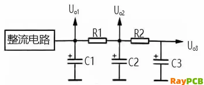
The π-type RC filter represents a significant advancement in filtering technology, combining multiple capacitors and resistors in a configuration that resembles the Greek letter π. This sophisticated approach provides superior filtering performance through a multi-stage attenuation process that systematically removes AC components while preserving DC voltage.
The circuit typically begins with a large input capacitor that provides initial filtering of the rectified voltage, removing the majority of low-frequency ripple components. The filtered signal then encounters a series resistance that works in conjunction with a second capacitor to create an additional filtering stage. This RC combination acts as a low-pass filter, further attenuating any remaining AC components that survived the initial filtering stage.
The design of π-type RC filters requires careful consideration of component values to achieve optimal performance. The input capacitor must be sized appropriately to provide adequate initial filtering without creating excessive inrush current that could damage rectifier diodes. The series resistance value represents a critical design parameter—insufficient resistance provides inadequate filtering, while excessive resistance causes significant DC voltage drops that reduce output voltage.
Multiple output taps can be implemented along the filter chain, providing various voltage levels with different degrees of filtering. Early taps in the circuit provide higher voltage levels with moderate filtering, while later stages offer lower voltages with superior ripple rejection. This flexibility allows a single filter circuit to serve multiple circuit requirements with varying noise tolerance levels.
π-Type LC Filter Circuits
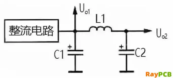
The π-type LC filter configuration replaces the series resistor with an inductor, creating a more efficient filtering system that maintains excellent AC rejection while minimizing DC voltage losses. This substitution leverages the inductor’s ability to present high impedance to AC signals while maintaining minimal resistance to DC current.
The advantages of LC filtering become particularly apparent in high-current applications where resistive voltage drops would be prohibitive. Unlike resistors, which dissipate power as heat regardless of current type, inductors provide frequency-selective impedance that targets only the unwanted AC components. This selective behavior allows LC filters to achieve superior filtering performance while maintaining higher efficiency and better voltage regulation.
The implementation of π-type LC filters requires attention to inductor specifications and behavior. Real inductors possess both inductance and resistance characteristics, with the resistive component contributing to voltage drops and power losses. High-quality filter inductors minimize this resistance while maximizing inductance, though such components typically involve higher costs and larger physical dimensions.
Active Electronic Filter Circuits
Basic Electronic Filter Implementation
Electronic filter circuits represent an evolution in filtering technology, incorporating active components such as transistors to enhance traditional passive filtering approaches. The basic electronic filter employs a transistor as an active filtering element, with its base circuit connected to an RC filter network that provides the filtering reference.
The transistor in this configuration functions as a voltage follower with current amplification capabilities. The RC network at the transistor’s base provides a filtered reference voltage, while the transistor’s emitter follows this voltage with the ability to supply significantly higher current to the load. This arrangement creates an equivalent capacitance effect that far exceeds the physical capacitor value, as the effective filtering capacitance becomes the product of the physical capacitor and the transistor’s current gain.
This amplification effect allows electronic filters to achieve superior filtering performance with smaller physical capacitors, addressing space and cost constraints common in modern electronic design. The transistor’s current gain effectively multiplies the filtering capacitor’s value, creating the electrical equivalent of a much larger capacitor without the associated physical bulk.
Electronic Regulator Filter Circuits
Advanced electronic filter designs incorporate voltage regulation components such as Zener diodes to provide both filtering and voltage stabilization in a single circuit. This combined approach addresses two critical power supply requirements simultaneously, creating systems that provide both clean and stable output voltage.
The Zener diode in these circuits establishes a stable reference voltage at the transistor’s base, ensuring consistent output voltage regardless of input variations or load changes. The series resistance limits current through the Zener diode while maintaining proper bias conditions for both regulation and filtering operations.
Compound transistor configurations can further enhance electronic filter performance, using multiple transistors in Darlington or similar arrangements to achieve even higher current gains. These advanced configurations multiply the effective filtering capacitance by the product of individual transistor gains, creating extremely effective filtering with minimal component requirements.
Design Considerations and Optimization
Component Selection Strategies
Successful filter circuit design requires careful attention to component specifications and their interaction within the complete system. Capacitor selection must consider not only capacitance value but also voltage rating, temperature coefficient, and ESR characteristics. Low ESR capacitors provide superior high-frequency filtering performance, while adequate voltage ratings ensure reliable operation under all circuit conditions.
Inductor selection involves balancing inductance value, DC resistance, current handling capability, and physical constraints. High-quality filter inductors feature low DC resistance to minimize voltage drops while providing adequate inductance for effective filtering. Core material selection affects both performance and cost, with ferrite cores offering good performance for most applications while more exotic materials may be required for demanding specifications.
Performance Optimization Techniques
Filter circuit optimization involves systematic analysis of ripple reduction requirements, voltage regulation needs, and efficiency considerations. Mathematical modeling can predict filter performance and guide component selection, while simulation tools allow verification of design approaches before physical implementation.
Load regulation characteristics must be considered throughout the design process, as filter circuit behavior can vary significantly with changing load conditions. Some filter configurations maintain consistent performance across wide load ranges, while others may require additional regulation circuitry for optimal performance.
Conclusion
Filter circuits represent an essential technology in modern electronics, enabling the conversion of raw rectified power into the clean, stable DC voltage that electronic systems require. Through understanding of fundamental filtering principles and careful application of various circuit configurations, engineers can design power supply systems that meet the demanding requirements of contemporary electronic applications.
The evolution from simple capacitor filters through advanced electronic filtering techniques demonstrates the continuous advancement in power supply technology. Each configuration offers distinct advantages and limitations, requiring engineers to carefully match filtering approaches to specific application requirements.
As electronic systems continue to demand higher performance and greater efficiency, filter circuit design remains a critical skill for electronics engineers. Mastery of these fundamental principles provides the foundation for tackling increasingly sophisticated power supply challenges in next-generation electronic systems.