Planar transmission lines are widely used in high-frequency and microwave circuits due to their ability to transmit electromagnetic signals efficiently. These transmission lines come in various forms, each with its own unique characteristics and applications. In this comprehensive article, we will explore the differences between coplanar waveguide, microstrip, stripline, and other planar transmission lines.
Introduction to Planar Transmission Lines
Planar transmission lines are a type of transmission line where the conductors are printed or etched on a dielectric substrate, typically a printed circuit board (PCB). These transmission lines are designed to guide and confine the electromagnetic waves within the dielectric medium, allowing for efficient signal propagation at high frequencies.
The choice of planar transmission line depends on various factors, such as frequency range, impedance requirements, fabrication constraints, and circuit complexity. Each type of planar transmission line offers unique advantages and trade-offs in terms of performance, manufacturability, and cost.
Coplanar Waveguide (CPW)
Structure and Characteristics
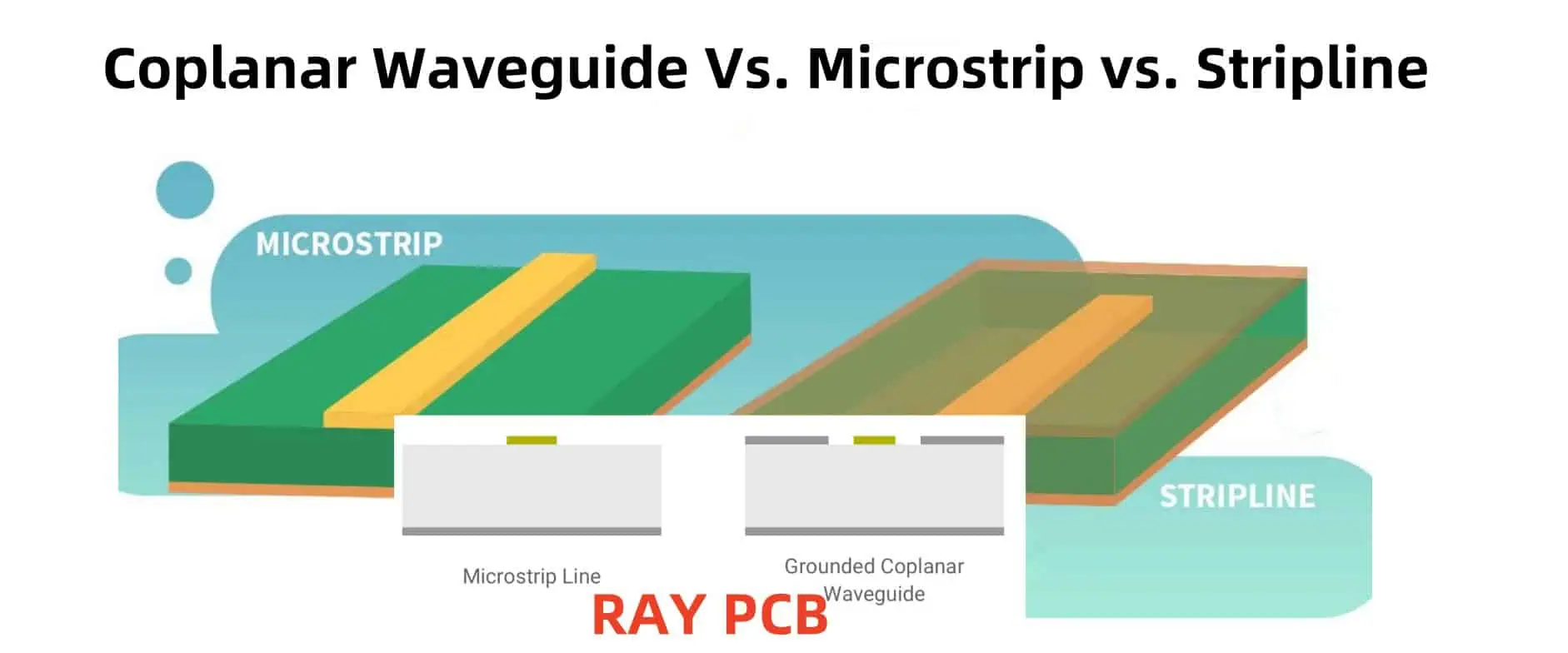
The coplanar waveguide (CPW) is a type of planar transmission line where the signal conductor and ground planes are on the same plane, separated by a dielectric material. The signal conductor is sandwiched between two ground planes, forming a coplanar structure.
Key features of a coplanar waveguide include:
- Simple and cost-effective fabrication process
- Suitable for both shielded and unshielded applications
- Excellent high-frequency performance
- Easy integration with active and passive components
- Relatively low dispersion and radiation losses
Applications
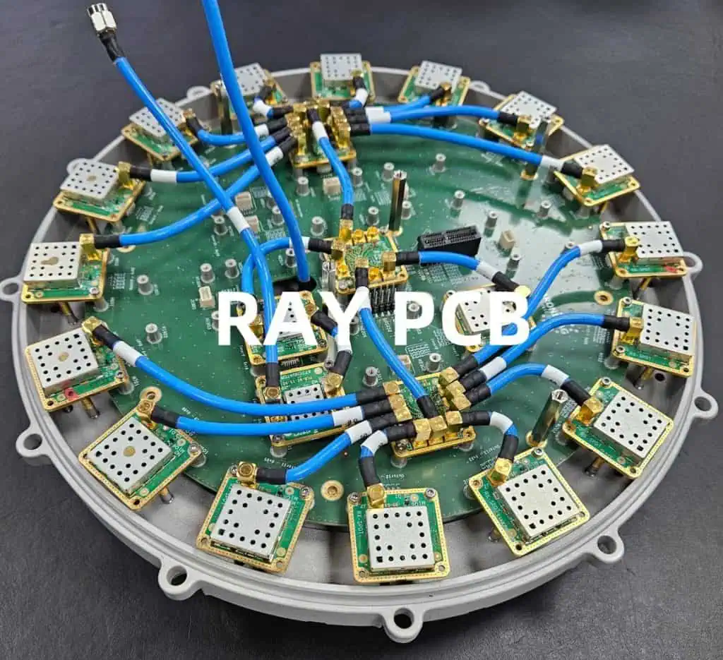
Coplanar waveguides are widely used in various high-frequency and microwave applications, such as:
- Monolithic Microwave Integrated Circuits (MMICs)
- Millimeter-wave and terahertz circuits
- Broadband and ultra-wideband circuits
- Antenna feed networks
- Interconnects and transitions in hybrid circuits
Microstrip
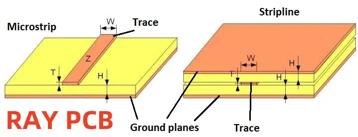
Structure and Characteristics
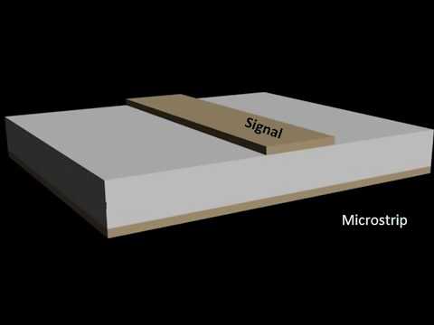
The microstrip is one of the most common and widely used planar transmission lines. It consists of a single conductor strip separated from a ground plane by a dielectric substrate.
Key features of a microstrip transmission line include:
- Easy fabrication and integration with other components
- Low cost and compact size
- Suitable for both analog and digital circuits
- Relatively high losses at higher frequencies
- Potential for radiation and crosstalk issues
Applications
Microstrip transmission lines are extensively used in various applications, such as:
- Radio Frequency (RF) and microwave circuits
- Antennas and antenna arrays
- Filters and couplers
- Mixers and amplifiers
- Printed Circuit Board (PCB) interconnects
Stripline
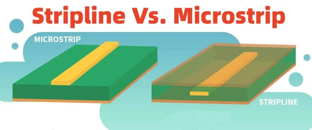
Structure and Characteristics
The stripline is a planar transmission line where the signal conductor is sandwiched between two ground planes, separated by dielectric layers. This configuration provides better shielding and reduces radiation losses compared to microstrip lines.
Key features of a stripline transmission line include:
- Excellent shielding and low radiation losses
- Low dispersion and crosstalk
- Suitable for high-frequency and high-speed applications
- More complex fabrication process compared to microstrip
Applications
Stripline transmission lines are commonly used in:
- High-speed digital circuits
- Microwave and millimeter-wave components
- Interconnects in multi-layer PCBs
- High-performance analog and mixed-signal circuits
Other Planar Transmission Lines
In addition to the coplanar waveguide, microstrip, and stripline, there are several other types of planar transmission lines, each with its own unique characteristics and applications. Here are a few examples:
- Slotline: A slotline is a planar transmission line where the signal is transmitted through a narrow slot etched in the ground plane. It is useful for various millimeter-wave and terahertz applications.
- Suspended Stripline: A suspended stripline is a variation of the stripline where the signal conductor is suspended in an air or foam dielectric, resulting in lower losses and higher performance at millimeter-wave frequencies.
- Inverted Microstrip: An inverted microstrip is a variation of the microstrip where the signal conductor is on the bottom layer, and the ground plane is on the top layer. This configuration is useful for integrating active components and shielding.
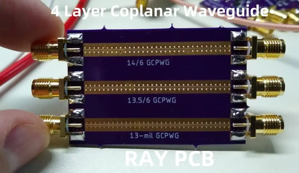
- Grounded Coplanar Waveguide (GCPW): A grounded coplanar waveguide is a variation of the CPW where a ground plane is added on the bottom layer, providing better shielding and reduced radiation losses.
- Coupled Planar Transmission Lines: Coupled planar transmission lines consist of two or more signal conductors in close proximity, allowing for coupling between the lines. These are used in couplers, filters, and other microwave components.
Comparison of Planar Transmission Lines
To better understand the differences between these planar transmission lines, let’s compare their key characteristics in a tabular format:
| Transmission Line | Fabrication Complexity | Shielding | Radiation Losses | Dispersion | Crosstalk | Typical Applications |
| Coplanar Waveguide (CPW) | Simple | Moderate | Moderate | Low | Moderate | MMICs, millimeter-wave circuits, broadband circuits |
| Microstrip | Simple | Poor | Moderate to High | Moderate | High | RF and microwave circuits, antennas, PCB interconnects |
| Stripline | Moderate | Excellent | Low | Low | Low | High-speed digital circuits, microwave components, multi-layer PCBs |
| Slotline | Simple | Moderate | Moderate | Low | Moderate | Millimeter-wave and terahertz circuits |
| Suspended Stripline | Complex | Excellent | Very Low | Very Low | Very Low | Millimeter-wave and terahertz circuits |
| Inverted Microstrip | Simple | Moderate | Moderate | Moderate | Moderate | Integration with active components, shielding |
| Grounded Coplanar Waveguide (GCPW) | Moderate | Good | Low | Low | Low | Shielded circuits, low radiation applications |
| Coupled Planar Transmission Lines | Moderate to Complex | Moderate to Good | Moderate | Moderate | Moderate | Couplers, filters, microwave components |
Frequently Asked Questions (FAQs)
- What is the main advantage of using a coplanar waveguide over a microstrip transmission line? The main advantage of using a coplanar waveguide is its simple and cost-effective fabrication process. Additionally, CPWs are suitable for both shielded and unshielded applications and offer excellent high-frequency performance.
- When should I choose a stripline over a microstrip transmission line? Stripline transmission lines should be chosen when you require better shielding, lower radiation losses, and lower dispersion compared to microstrip lines. They are particularly suitable for high-frequency and high-speed applications, as well as multi-layer PCB interconnects.
- What are the trade-offs when using a suspended stripline? While suspended striplines offer very low losses and excellent performance at millimeter-wave frequencies, they are more complex and expensive to fabricate compared to other planar transmission lines. Additionally, their open structure may make them more susceptible to environmental effects and mechanical stress.
- Can planar transmission lines be used for high-power applications? Most planar transmission lines are primarily designed for low to moderate power applications. For high-power applications, special considerations need to be taken into account, such as using larger conductor widths, thicker substrates, and additional cooling mechanisms to dissipate heat.
- How do I choose the appropriate planar transmission line for my application? Choosing the appropriate planar transmission line involves considering several factors, including the frequency range, power levels, circuit complexity, fabrication constraints, and performance requirements. It is often beneficial to consult with experienced RF and microwave engineers or refer to design guidelines and best practices for your specific application.
By understanding the differences between coplanar waveguides, microstrip, stripline, and other planar transmission lines, you can make informed decisions and select the most suitable option for your high-frequency and microwave circuit designs.