Blinking LED Circuit with Schematics and Explanation

Light-emitting diode is known simply as โ€œthe LEDโ€.

The Schematic Diagram of Flashing LED Application

The diode made of a compound of gallium, arsenic and phosphorus, that can emit visible light when electrons are combined with holes. So it can be used to make LED.

YouTube video

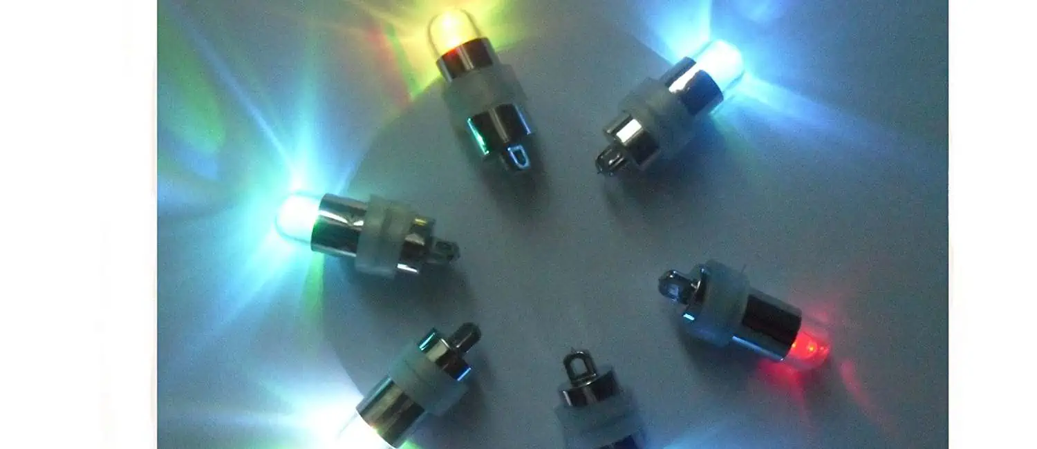
LED is used as an indicator light in circuits and instruments, It can also be displayed in text or number.

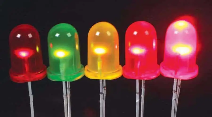
Gallium arsenide phosphide diodes emit red light;

Gallium phosphide diodes emit green light;

Silicon carbide diodes emit yellow light.

As shown in the figure, It is the circuit diagram of flashing single LED application.

The flashing LED operates at a low hertz frequency, it is easy to attract peopleโ€™s attention. So it can be widely used in various alarm circuits, such as temperature, liquid level, and voltage limit alarm circuits.

It is a type of semiconductor diode that can convert electrical energy into light energy;

Both Led and ordinary diode, consists of a PN junction with unidirectional conductivity.

The Schematic Diagram of Flashing LED Application

Introduction

Blinking LED circuits are used in a wide range of simple electronic projects to demonstrate digital logic and timing fundamentals. By automatically turning an LED on and off repeatedly, useful visual indications, alerts, and effects can be created.

This article provides schematic diagrams and explanations of common blinking LED circuit implementations using 555 timers, microcontrollers, and discrete transistor designs. Both astable oscillators for continuous blinking and monostable time delay configurations are covered.

555 Timer Astable Blinking LED

The 555 timer integrated circuit configured as an astable multivibrator provides a simple method for generating a blinking LED:

How it Works

  • 555 setup as astable oscillator charging/discharging between C1/R1 and C2/R2.
  • Output square wave drives transistor which switches LED on/off.
  • Flashing rate determined by R1, R2, C1, C2 values per 555 astable equations.
  • Output duty cycle depends on ratio of R1/R2. Equal values provide 50% duty cycle.
  • LED current limited by R3. R4 pulls down transistor base when off.

This basic circuit using just a 555 timer and few components provides continuous LED blinking. Frequency and duty cycle can be adjusted via resistor and capacitor values.

555 Monostable Blinking LED

A 555 timer monostable configuration generates timed pulses to blink an LED:

How it Works

  • Pushbutton trigger generates a defined one-shot pulse from 555 monostable on each press.
  • Output pulseturns on transistor, lighting LED for duration of pulse.
  • Timing components R1, R2 and C1 determine pulse width.
  • Subsequent button presses restart timing cycle blinking LED again.
  • Optional biasing components (dotted) keep transistor OFF in idle state.

This creates a manually triggered blinker that illuminates the LED for a timed duration with each activation. Can produce attention getting flashes.

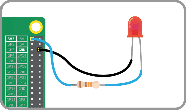
Microcontroller Blinking LED

Microcontrollers provide fully software controllable blinking LED capabilities:

How it Works

  • LED connected to GPIO pin of microcontroller.
  • Software loops to toggle I/O pin HIGH/LOW at desired blink frequency.
  • Timer peripheral used to control ON and OFF duration.
  • Duty cycle easily adjusted in software to provide desired blink pattern.
  • Current limiting resistor protects I/O pin from excessive current draw.

Microcontroller blinkers are fully customizable in software and avoid any external components beyond the LED itself. Timing, duty cycles, and patterns can be reconfigured on the fly.

Transistor Astable Blinker

Discrete transistors can also implement an astable multivibrator blinking circuit:

Show Image

How it Works

  • Cross-coupled transistor pair switches each other on/off repeatedly.
  • Powered by collector supply Vcc.
  • R1/R2 bias transistors just below turn-on threshold when other transistor is ON.
  • C1/C2 timing capacitors charge through collectors controlling blink rate.
  • Q1 collector output drives external LED.
  • R5 limits LED current. R3/R4 provide DC bias.

This all-transistor astable circuit provides high current drive capacity for multiple LEDs if needed. Timings easily adjustable through R and C values.

JFET Relaxation Oscillator Blinker

JFET transistors can implement simple relaxation oscillator blinker circuits:

How it Works

  • Capacitor C1 charges through R1 when JFET is OFF.
  • When voltage across C1 reaches JFET gate threshold, it turns ON rapidly discharging capacitor and lighting LED.
  • JFET turning ON forces its own gate low via R2 turning device back OFF.
  • Circuit repeats charging C1 and blinking LED.
  • R4 limits LED current. R3 provides bias.

This self-blinking circuit uses only a JFET transistor and passive components. Frequency controlled through R1/C1 time constant.

Summary

  • Blinking LED circuits provide visual alerts and indications using electronic oscillators and digital timing.
  • 555 timers as astable or monostable oscillators offer simple blinker circuits.
  • Transistor multivibrator and JFET relaxation oscillator designs enable discrete component LED blinkers.
  • Microcontrollers allow fully software controlled blinking for maximum flexibility.
  • Combine blinking visual outputs with other circuit functions like sensing for integrated systems.

Blinking LEDs find countless applications in electronic projects to visually indicate states and activities in an energy efficient manner.

FAQ

What are some application examples of blinking LED circuits?

Some common applications are visual indicators on electronic devices, heartbeat or measures indicators, flashing alerts when events occur, lighting effects, toy and sculpture lighting, timing games, and visual metronome or speed displays.

How do you calculate the blink frequency for 555 timer circuits?

The formulas for a 555 astable oscillator provide the blink frequency based on resistor and capacitor values. Duty cycle is controlled by the ratio of RA to RB. Refer to 555 datasheets for exact equations.

How fast can an LED be blinked by a microcontroller?

Microcontrollers can easily blink most LEDs well into the hundreds of Hertz. Using timer hardware peripherals and interrupts allows blinking at kilohertz frequencies for most LED types.

What determines the blink intensity of an LED?

Blink intensity is controlled by the LED drive current. Higher current causes greater light intensity. Series current limiting resistors can adjust intensity by changing the voltage across the LED.

How do you make an LED blink slower?

For 555 timers, use larger timing capacitor values and/or smaller resistor values to increase the RC time constant. For microcontrollers, increase the software delay timing. For transistor circuits, increase capacitance and/or resistance to extend timing.

Stepper Motors Basics: Types, Uses, and Drive Schematic Diagram

A stepped motor which could convert an electric pulse signal into an angular displacement or linear displacement and its driver circuit diagram.

A stepping motor is an open-loop control element stepping motor that converts an electrical pulse signal into an angular displacement or a linear displacement. In the case of non-overload, the speed and stop position of the motor only depend on the frequency of the pulse signal and the number of pulses, and are not affected by the load changes. When the stepper driver receives a pulse signal, it drives the stepper motor to rotate a fixed angle in the set direction, called โ€œstep angleโ€, and its rotation is performed step by step at a fixed angle.

It is one of the most commonly used control electronic components in industrial control and instrumentation. It has the characteristics that the input pulse is proportional to the motor shaft. It is widely used in intelligent robots, floppy disk drives and data machine tools. The most suitable system for microcomputer-controlled stepper motors is the 20BY-0 stepper motor. It uses a +5V DC power supply with a step angle of 18 degrees and the motor coil consists of four phases.

Stepper Motor and Drive Schematic Diagram

Introduction

YouTube video

Stepper motors are brushless DC electric motors that move in discrete angular steps in response to digital pulse signals. They are precisely controllable and can be used in open loop position control systems without the need for feedback sensors.

Stepper motors are used extensively in industrial automation, robotics, 3D printers, CNC machines, and many other applications requiring precise positioning and speed control. They provide excellent low speed torque and response to digital inputs.

This comprehensive guide covers the operating principle of stepper motors, drive methods, common types and configurations, typical applications, and drive circuit schematic implementations.

How Stepper Motors Work

Stepper motors consist of a rotor containing permanent magnets and a stator containing electromagnets (windings). Applying current pulses to the windings generates magnetic fields which interact with the rotor magnets, causing rotational movement one step at a time.

Stepper Motor Rotation (Image Credit: Bakon/Wikimedia)

Some key operating characteristics of stepper motors:

  • Motion occurs in discrete steps measured in degrees (Most common is 1.8ยฐ/step or 0.9ยฐ/step)
  • Accurate positioning and repeatability – errors less than 5% of per step angle
  • Open loop control – No feedback sensors required
  • Driven by digital pulse trains from controllers
  • Torque optimized for low speed high precision applications
  • High holding torque when not moving resists external forces
  • Can be miniaturized down to tiny step angles enabling precision micro-positioning

Understanding the stepping sequence and drive methods allows proper control of stepper motors.

Drive Methods

Stepper motors are commutated by energizing the phase windings in a sequential pattern to rotate the shaft. Two primary drive methods are used:

Wave Drive (1 Phase ON)

Only one winding is energized at any time. Rotor magnet aligns with magnetic field produced by active winding before next step occurs.

Provides greater torque at lower speeds. Resonances can occur at higher speeds.

Wave Drive Sequence (Image Credit: Festo Didactic)

Full Step Drive (2 Phase ON)

Two windings are energized simultaneously to produce stronger torque. Minimizes resonances.

Cannot achieve very low speeds. Provides higher torque across operating range.

Full Step Drive Sequence (Image Credit: Festo Didactic)

Proper selection of drive mode depends on required speed and torque. Controllers allow selecting different drive modes.

Stepper Motor Types

Stepper motors are classified based on their internal construction:

Variable Reluctance

Contain salient pole stator with concentrated windings. Multi-toothed rotor provides varying magnetic reluctance as it rotates. Simple and inexpensive construction.

Permanent Magnet

Have magnetized rotor with defined poles. Stator has distributed windings. Provides good torque and low resonance issues. Most common type.

Hybrid

Combine permanent magnet rotor with salient pole stator. Provides high torque, low resonance, good speed range. Most advanced and powerful type.

The number of stator teeth determine the step angle. More teeth provide finer resolution but require more switching.

Stepper Motor Configurations

Beyond the internal construction, stepper motors are also classified by their physical size, shaft type, and operating voltages:

Size and Frame

  • Very small steppers < 28 mm used in precision instruments. 0.9ยฐ step angle.
  • Small steppers between NEMA 8 – 17 sizes used in automation. 1.8ยฐ step angle.
  • Large NEMA 23-34 frame steppers used in high torque applications. 1.8ยฐ step angle.
  • Pancake or slim profile steppers optimized for tight spaces.

Shaft Type

  • Standard round shaft – most common
  • D-shaped shafts prevent slipping of couplings
  • Geared – have integrated gearheads to increase torque
  • Hollow shaft – for applications like driving lead screws

Voltage Rating

  • Low voltage steppers – 12 or 24V types common. Higher currents.
  • Medium voltage – 36 or 48V rated. Used in automation.
  • High voltage – for precision or high power steppers. Up to 300V.

Combine winding configuration, drive mode, frame size, shaft and voltage rating to select optimal stepper.

Stepper Motor Performance Specs

Key specifications to evaluate stepper motor performance:

  • Steps per Revolution – Typically range from 24 to 400 steps/revolution. More steps enables greater positioning precision.
  • Step Angle – Angle moved per step. Common values are 0.9ยฐ, 1.8ยฐ, 7.5ยฐ and 15ยฐ. Smaller step angle provides higher resolution.
  • Torque – Rated holding and pull-out torque values. Higher torque allows faster accelerations under load.
  • Voltage – Rated voltage and input current determines power input needs.
  • Inductance – Higher is better for drivability at higher speeds but reduces torque. Values from 1mH to 50mH typical.
  • Resistance – Lower resistance enables higher torque output. Range is typically 1-5ฮฉ per phase.
  • Inertia – Lower rotor inertia allows faster acceleration and response.
  • Accuracy – Deviation from intended step angle measured in arcminutes. Sub-arcminute accuracy is achievable.

Review rated specifications against the application’s resolution, torque, speed, and accuracy requirements when selecting an optimal stepper motor.

Stepper Motor Drives

Stepper motors require properly designed drive circuits to energize their phases in coordination with input step and direction signals. Here are the key functions stepper motor drivers perform:

Power Amplification

Increase current and voltage levels of control signals to adequately drive motor windings. Typically chopper or linear drives used.

Stepping Sequence Generation

Translate step and direction inputs into a sequence for energizing the phase windings. Microstepping capability is desirable.

Current Control

Vary winding currents to optimize torque output. Lower current at high speeds to overcome inductive impedance.

Protection Circuits

Detect error conditions like missed steps or overtemperature and respond appropriately to prevent damage.

Feedback Interfaces

Provide connections to external encoders or sensors when closed loop operation is needed.

Command Inputs

Step and direction signal inputs dictate motor motion. Additional control inputs like enables may be included.

Properly designed drives ensure smooth and reliable stepper motor operation and protect against malfunctions.

Basic Unipolar Driver

Here is a basic unipolar driver for a variable reluctance stepper:

  • ULN2003 Darlington transistor array provides 500mA current rating per channel. 8 channels total.
  • Diodes protect against back EMF when winding currents are switched.
  • Resistors limit current through windings. Can alter values to change maximum current levels.
  • Inputs must be energized in proper sequence to step motor.
  • Only one winding active at any time. Limited torque capability.

Low component count makes this a simple and inexpensive drive choice but performance is limited.

Basic Bipolar Driver

A basic bipolar driver energizes two windings simultaneously:

Show Image

  • Dual H-Bridge (L298N) allows 4 quadrant operation of windings.
  • Allows current in both directions through windings enabling bipolar drive.
  • Higher performance but increased component count over unipolar design.
  • Provides up to 2A per winding. Higher than unipolar drives.
  • Fast switching time < 100ns.

Bipolar drive with H-bridges provides good performance for small to mid-sized steppers.

Microstep Driver

Microstepping divides steps into smaller increments. Typical microstep resolutions are 1/8, 1/16, 1/32, 1/64 step:

  • Sinusoidal microstepping currents smooth motor operation and provide position interpolation.
  • Microstep table maps control input state to sine wave DAC value.
  • On-chip DAC and PWM generate sinusoidal current profiles in windings.
  • Chopper circuits allow microstepping and current control capability.
  • External potentiometer sets maximum current level.

Microstepping allows very fine resolution motion and smoothing with stepper motors.

Integrated Stepper Controller

Integrated stepper controllers contain drive electronics, sequencing logic, and microcontroller:

  • Microcontroller generates control signals and sequences drive waveform based on incoming step and direction inputs.
  • Integrated motor drivers with current control. May include thermal shutdown.
  • Onboard supply generates motor voltages from main DC input.
  • Status indicators and I/O allow monitoring and interfacing.
  • Parameters and drive modes configurable through communication interfaces.

All-in-one integrated controllers simplify implementation with advanced features and protection.

Stepper Motor Applications

Stepper motors provide many advantages for precise positioning in automation, robotics, instruments, and other applications:

  • CNC Machines – For precisely controlling cutting tools and workpiece position.
  • 3D Printers – High precision positioning of print heads over multiple axes.
  • Scanners & Plotters – Provide linear motion and positioning for optics.
  • Robots – Allow precise joint control and position feedbackless operation.
  • Pick-and-Place – X-Y positioning for PCB assembly and packaging machines.
  • Laser Cutters – For accurate motion and focusing of optics.
  • Textiles – Provide incremental stitching motion in sewing machines.
  • Displays – Used in meter movements, gauge mechanisms, advertising displays.
  • Valves – Precise control over fluid flow without complex feedback.

Stepper’s excellent response to digital inputs makes them ideal for computer controlled automation tasks requiring high precision.

Summary

  • Stepper motors provide precise digital control of rotational position without feedback sensors.
  • Operation based on magnetic field interactions between stator windings and rotor magnets.
  • Driven by pulse train inputs that sequence the winding energization to step the motor.
  • Major types include variable reluctance, permanent magnet, and hybrid steppers.
  • Driver circuits amplify signals and provide sequencing and protection. Microstepping enables fine increments.
  • Widely used in automation, robotics, CNC machines, 3D printers and other applications requiring high precision motion under digital control.

FAQ

What are the typical step angles for stepper motors?

Common step angles include 0.9ยฐ, 1.8ยฐ, 7.5ยฐ, 15ยฐ, and 30ยฐ. Smaller step angles allow higher precision but require more switching. 0.9ยฐ and 1.8ยฐ are most common for fine control.

What is the difference between unipolar and bipolar stepper motors?

Unipolar steppers only have current flowing in one direction through their coils, while bipolar motors reverse current direction providing higher torque. Bipolar motors require full H-bridge drivers.

Can stepper motors be used in closed loop systems?

Yes, stepper motors can incorporate rotary encoders or resolvers to provide position feedback. The controllers can use PID control in a servo loop to achieve even better precision and compensation.

Why are stepper motors operated at lower speeds?

The construction of stepper motors makes them best suited for operation below 1000 RPM. At higher speeds, resonances, switching delays, and inductance effects impair torque and control.

What causes lost steps in a stepper motor?

Exceeding torque limits, accelerating too quickly, too high a speed, or electrical noise can all cause missed steps and loss of synchronism. Proper drive design and torque margins prevent lost steps in most cases.

What is transistor inverter circuit?

In remote villages, there is often  power outages. Some universities will also have power outages at night, and those who like to stay up late will not have electricity. But thatโ€™s okay, you can solve this problem.

This is very easy to make an inverter that can turn the 12V supply voltage to be 220V. The circuit is driven by a multivibrator consisting of BG2 and BG3, and then driven by BG1 and BG2 to control BG6 and BG7 operation.

The oscillating circuit is powered by the regulated power supply of the BG5 and DW groups, which makes the output frequency relatively stable. At the time of production, we can choose the  commonly used AC transformers with dual 12V output. A 12V battery can be selected as needed.

This schematic diagram can also be used for small generator for home use.

The Schematic Diagram of Dual 12v Output Transistor Inverter

Introduction

A transistor inverter circuit converts a digital input signal to its opposite logic level at the output. For example, when the input is HIGH the output will be LOW and vice versa. Inverters play a key role in digital logic systems by providing signal inversion, buffering, logic level shifting, clock generation and other functions.

Inverters form the fundamental building block for more complex digital logic gates and functions. This article provides an overview of transistor-based inverter circuits, their operation, key parameters, types and applications.

Inverter Basics

An inverter uses an amplifying device like a transistor connected in a switching configuration to generate the inverted output:

  • When the input is LOW, the amplifying device turns ON pulling the output HIGH.
  • When the input is HIGH, the device is OFF and the output is pulled LOW through the load resistor.

This functionally inverts the logic level between input and output. The amplifying element provides gain to ensure solid logic HIGH and LOW voltage levels.

Basic Inverter Functional Diagram

Some key characteristics of inverters:

  • Gain should be higher than 1 for unambiguous logic levels
  • Provide high input impedance and low output impedance
  • Capable of high speed operation with fast switching
  • Output inverted copy of input waveform
  • Support fan-out to drive multiple gate inputs

Properly designed inverters are critical building blocks for reliable digital systems.

BJT Inverter

Here is a simple inverter circuit using a bipolar junction transistor:

When the input is LOW (< 0.7V), the transistor is OFF. Output is pulled HIGH through Rc.

When input is HIGH (>0.7V), transistor turns ON and pulls output LOW via collector-emitter path.

Resistor RB provides biasing to keep transistor OFF when input is LOW. Capacitor CE helps speed up switching by providing current bursts.

Key characteristics:

  • Slow compared to MOSFET circuits due to minority carrier charge storage
  • Input HIGH level must exceed 0.7V (base-emitter diode drop)
  • Output swing typically 0.2V to (Vcc – 0.2V)
  • Low input impedance, moderate output impedance

Simple and inexpensive but performance limited. Better for lower speed applications.

MOSFET Inverter

Here is an inverter using a MOSFET transistor:

When input is LOW (<threshold voltage), MOSFET is OFF, output pulled HIGH.

When input is HIGH (>threshold voltage), MOSFET turns ON discharging output to ground.

No biasing network needed compared to BJT version.

Key characteristics:

  • Very high speed since no minority carrier storage
  • Low input threshold voltage (~1-2V)
  • Rail-to-rail output swing potential
  • High input impedance, low output impedance
  • Draws no current when OFF

Much faster switching speeds than possible with BJTs. Widely used for high performance digital logic.

CMOS Inverter

CMOS inverters use complementary NMOS and PMOS transistors:

When input is LOW, PMOS is ON pulling output HIGH. NMOS is OFF.

When input is HIGH, NMOS turns ON and discharges output LOW. PMOS is OFF.

No current flows from supply to ground when in static state. Very low quiescent power.

Provides excellent noise immunity and high gain. Standard for modern digital ICs.

Key Inverter Characteristics

Some key performance parameters for inverters:

  • Propagation Delay: Time taken to switch output state after input change. Need very low (ns range) for high speed operation.
  • Rise/Fall Time: Time taken for output voltage to transition between logic levels. Lower is better for high speed.
  • Gain: Ratio of output to input voltage. Should exceed one for robust noise margin.
  • Fan-out: Number of standard input gates that can be reliably driven by the output. Higher is better.
  • Power Consumption: Quiescent and dynamic power. CMOS is most efficient topology.
  • Noise Immunity: Ability to reject noise coupling and avoid false triggering. VIL and VIH levels determine immunity.

Optimizing these parameters through careful transistor sizing and biasing is key to designing robust high performance inverters.

Types of Inverters

Some common types of inverters used in digital systems include:

  • Buffer Inverters – Provide isolation between circuits while inverting logic level. Used to prevent loading effects.
  • Logic Level Shifters – Convert between voltage levels like TTL and CMOS. Provides compatibility.
  • Clock Inverters – Special fast inverters designed to provide inverted clock signals with precision timing.
  • Schmitt Trigger Inverters – Provides hysteresis for noisy inputs. Cleans up waveforms.
  • Rail-to-Rail Output Inverters – Swings output from supply rail to ground. Improves high/low logic levels.
  • Open Drain Output Inverters – Used when wired-AND logic is needed. Pulls output low but does not drive high.

Selecting the right inverter type enhances performance for the target application.

Inverter Circuits Examples

Here are some example inverter circuit implementations:

Buffer Inverter

Isolates loading on upstream gate/source. Boosts current drive for higher fan-out.

Level Shifter

Converts 1.8V CMOS logic to 5V TTL input requirements. Provides inter-logic family translation.

Schmitt Trigger Inverter

Provides hysteresis for noisy waveforms. Cleans up slow rise/fall times.

Inverter Applications

Inverters play a vital role in many digital logic systems:

  • Oscillator and clock generation circuits
  • Driving logic signals across long PCB traces
  • Interfacing logic families with incompatible voltages
  • Buffering high fan-out signals to prevent overloading
  • Inversion of control and timing signals
  • Waveform shaping of noisy digital signals
  • Logic level translation between circuits

Any design needing signal inversion, buffering, gating, or logic level shifting will require inverters as fundamental building blocks.

Summary

  • Inverters use transistor amplifiers to invert the logic level between input and output.
  • BJT, MOSFET and CMOS are common transistor types used to build inverters.
  • Key performance factors include propagation delay, speed, gain, fan-out, noise immunity.
  • Many circuit variations exist optimized for functions like buffering, level shifting, noise reduction.
  • Inverters are core components in digital logic, timing generation, signal conditioning, and translation applications.

Understanding inverter circuits provides the foundation for designing more complex digital logic functions.

FAQ

What is the difference between inverter and NOT gate?

Inverters and NOT gates perform the same logic function of inverting the input signal. Inverter tends to refer to transistor circuit implementations while NOT gate can be used when discussing abstract boolean logic functions.

Why use an inverter vs direct connection?

Inverters provide gain, isolation, and logic level shifting. This prevents distortion of the original signal. A direct connection can load down source circuits and potentially cause malfunction.

What is the basic structure of all inverter circuits?

A switching element (transistor) with load configured to invert input to output. BJT, JFET, MOSFET switching devices with resistors as loads are common. The active device provides amplification.

How does an inverter provide logic level shifting?

The inverter can operate between higher and lower supply voltages. The input threshold and output swing adapt to the inverter’s own supply levels allowing translation.

Why use Schmitt Trigger inverters?

Schmitt Trigger inverters incorporate positive feedback to provide hysteresis in the switching thresholds. This makes them less sensitive to noisy input signals and improves waveform shaping.

What is Digital Thermometer Circuit Diagram ?

An electronic thermometer circuit diagram with high measurement accuracy, memory and beep tips for human body temperature.

The electronic thermometer consists of a temperature sensor, an LCD monitor, a button battery, a special integrated circuit and other electronic components.

Compared with the traditional mercury glass thermometer,electronic thermometer can measure the body temperature quickly and accurately,has the advantages of convenient reading, short measurement time, high measurement accuracy, energy memory and buzzing cues. The circuit of the electronic thermometer is shown as below, thermal power RT stares and R1, R2, R3 and RP1.When the temperature is 20 โ„ƒ, select R1, R3 and adjust the RPL to make the bridge a balance.

Electronic Thermometer Diagram

Introduction

A digital thermometer circuit diagram illustrates the electronic components and connections required to construct a thermometer that provides temperature readings in numeric format. Unlike analog thermometers that use a mercury column, bimetallic coil, or other mechanical sensor, digital thermometers convert temperature into an electrical signal that is digitized using analog-to-digital conversion and displayed.

Understanding the circuitry allows constructing simple to more complex digital thermometers. The key components include temperature sensors, analog signal conditioning, microcontrollers or display drivers, displays, and power supplies. Common sensing elements used include thermistors, RTDs, and thermocouples.

This article will provide an overview of several typical digital thermometer circuit implementations and their diagrams.

How Digital Thermometers Work

Here are the key steps in how a digital thermometer functions:

  • A temperature sensor converts the ambient temperature into an analog electrical signal that varies based on temperature.
  • The analog signal is conditioned and amplified through circuitry. This improves the signal quality.
  • The amplified signal is fed into an analog-to-digital converter (ADC) to digitize the temperature value.
  • A microcontroller or display driver chip reads the digitized temperature from the ADC.
  • The chip outputs the numeric temperature reading on a digital display like an LCD.
  • Power supply circuitry provides regulated voltage to the components.

By understanding this sequence, we can now examine some sample digital thermometer circuit diagrams.

Simple Thermistor Thermometer

Here is a basic digital thermometer circuit using a thermistor as the temperature sensing element:

This circuit uses just a few low cost components:

  • Thermistor – Temperature dependent resistor. Resistance drops non-linearly as temperature rises. Provides analog temperature signal.
  • Comparator – Produces a digital output by comparing thermistor voltage against known reference voltage.
  • 555 Timer – Configured in astable mode to produce clock pulses for the counter. Clock frequency varies based on thermistor resistance.
  • Counter – Counts clock pulses from 555 timer. Higher temperature causes higher clock frequency and thus higher counter value.
  • Decoder & Display – Translates counter output to drive the 7-segment LED display. Shows 2-digit temperature reading.
  • Reference Voltage – Provides stable voltage threshold for comparator. Set based on thermistor specs.

This simple circuit can measure over a narrow range of ~50ยฐC with 1-2ยฐC accuracy. Wider range thermometers require additional components.

LM35 Based Thermometer

YouTube video

The LM35 linear temperature sensor makes an excellent choice for more accurate digital thermometers:

  • LM35 Sensor – Integrated analog temperature sensor with linear +10mV/ยฐF output. High accuracy and low self heating.
  • Op-Amp – Configured as amplifier to boost LM35 output to readable voltage levels. Gain sets resolution.
  • ADC – Built-in analog-to-digital converter transforms amplified signal into digital values.
  • Microcontroller – Reads digitized temperature from the ADC channel and calculates temperature based on ADC reference voltage.
  • LCD – Microcontroller outputs temperature reading directly to LCD display. Can add ยฐF or ยฐC symbol.

This circuit allows much wider range and better than 1ยฐC accuracy with proper calibration. The LM35 enables a very linear and stable thermometer.

Multi-Sensor Thermometer

Here is a circuit for a versatile thermometer using multiple sensor types:

  • Instrumentation Amp – Differential amplifier subtracts voltage across RTD sensor to produce amplified temperature signal. High common mode noise rejection.
  • Thermocouple Amp – Amplifies small thermocouple voltage. Cold junction compensation circuit removes reference junction error.
  • Thermistor network – Voltage divider circuit produces thermistor signal readable by ADC.
  • ADC – Digitizes signals from all three sensors using input multiplexer and single ADC.
  • Microcontroller – Manages ADC measurements. Applies linearization and conversion algorithms specific to each sensor type.
  • Display – Shows current reading. Can display temperature from selected sensor.

This flexible design supports thermocouples, RTDs, and thermistors. The microcontroller software provides cold junction compensation and linearization for accurate readings from multiple sensor types.

Isolated Thermocouple Thermometer

For very high temperature measurements with thermocouples, an isolated circuit is required for safety and noise rejection:

  • Thermocouple – Acts as the temperature transducer based on differential voltage produced by dissimilar metal junctions.
  • Isolation Amplifier – Provides electrical isolation and protects low voltage circuitry from high common mode voltages. Also removes noise.
  • Cold Junction Compensator – Specialized integrated circuit measures reference junction temperature and compensates voltage to eliminate reference errors.
  • ADC – Digitizes the compensated thermocouple voltage for the microcontroller. High resolution ADC improves accuracy.
  • Microcontroller – Applies linearization algorithms specific to the thermocouple type. Calculates and displays temperature.
  • LCD Display – Shows current temperature reading up to 3-4 digit precision.

The combination of isolation amplifier and cold junction compensation allows this circuit to accurately measure very high temperatures in industrial environments.

Summary

  • Digital thermometers convert temperature into an electrical signal and then digitize it to display a numeric temperature reading.
  • Key components include temperature sensors, amplifiers, ADCs, microcontrollers, displays, and power supplies.
  • Popular sensors used include thermistors, RTDs, thermocouples, and integrated sensors like the LM35.
  • Circuit techniques like isolation, linearization, and cold junction compensation help improve measurement accuracy.
  • A microcontroller running sensor-specific code allows a single circuit to support multiple sensor types.
  • Digital thermometer circuits can be very simple or highly complex depending on the required measurement range and precision.

FAQ

What are the main components of digital thermometer?

The core components are the temperature sensor, signal conditioning circuitry, analog-to-digital converter, microcontroller/display driver, display, and power supply. Additional components improve linearity, isolation, accuracy, etc.

What temperature sensor is most accurate?

Platinum RTD sensors provide the highest accuracy and stability. However integrated sensors like the LM35 also offer excellent linearity and precision. Thermocouples are highly versatile for wide temperature range but need compensation.

What communication protocols are used in digital thermometers?

Many industrial digital thermometers use HART, Profibus, or Modbus for digital communication overtwisted pair wires or RS-485 links. This allows remote temperature monitoring and digitization.

How does software improve digital thermometer accuracy?

Linearization algorithms running on the microcontroller improve sensor accuracy by correcting non-linearities inherent in devices like thermistors and thermocouples over their operating range.

How does isolation improve digital thermocouple thermometers?

Isolation amplifiers prevent ground loops, reject common mode noise, and protect internal low voltage circuitry from the high voltages that can be produced by thermocouples monitoring very high temperatures in industrial processes.

What is Emergency Lighting Circuit Diagram ?

Emergency lighting is a type of lights that can effectively illuminate and display exit passageway or can continue to work without interruption when the normal lighting power supply fails,  Widely used in public places where can lighting without intermittent . The emergency lighting fixture is composed of a light source, a light source driver, a rectifier, an inverter, a battery pack, a logo lamp housing something like that.

Here is a circuit diagram of an emergency lighting made with LES.

The circuit operation of the device is shown in Figure 1. Power outages are a recurring thing, but in some cases power outages are not allowed (such as ongoing surgery). The circuit designed with LSE is simple and fully automated. When there is 220V AC power, the illumination lamp H1 is lit, and the โ‘ฃ pin of the LSE output with high level output, the Transistor VT is turned off, and the relay J is in a release state, so the DC lamp H2 is not lit. Once power cut, H1 goes out, and the LSEโ€™s โ‘ฃpin outputs a low level. At this time, the Transistor VT is conduction, the relay J is pulled in, the power of the illumination lamp H2 is connect, the H2 is automatically lit, and the transition between the two lamps is almost no break Intermittent.

Emergency lighting is still an important product required in against fire safety measures. In the event of an emergency, such as an earthquake, fire or circuit failure, the power supply is suddenly interrupted and all light sources have ceased to operate. At this point, it must provide reliable illumination immediately and indicate the direction of evacuation and the location of the emergency exit, in order to ensure the people who are in dark can evacuate

An Emergency Lighting Circuit Diagram

Introduction

An emergency lighting circuit diagram depicts the electrical connections and components of a system that provides backup illumination during power outages. Emergency lighting is essential for building safety by providing low level lighting to aid in emergency egress when normal lighting fails.

The emergency lighting circuit includes batteries, chargers, indicators, controls, and the specialized light fixtures needed to provide emergency lighting in buildings and public spaces as required by electrical and fire safety codes. Understanding emergency lighting circuits through their circuit diagrams is important for installation, inspection, and maintenance.

This article provides an overview of the key components and typical wiring diagrams used in emergency lighting installations.

Purpose of Emergency Lighting

Emergency lighting serves a vital safety function in buildings:

  • Illuminates exit paths to allow occupants to evacuate safely during emergencies or power loss.
  • Provides minimum illumination for critical areas like stairwells, aisles, corridors, ramps, and passageways.
  • Allows emergency responders to access and navigate a building in blackout conditions.
  • Reduces panic by providing some lighting during sudden power failures.
  • Serves as a backup to normal lighting system in case of electrical failure.
  • Mandated by national and local electrical, building, and fire codes for most public buildings. Exceptions sometimes made for small residential spaces.

Proper emergency lighting installation is crucial. The circuitry must be reliable and wire correctly to fixtures intended for emergency use.

Key Components of Emergency Lighting Circuits

YouTube video

A typical emergency lighting system consists of the following major components:

Backup power source – Usually rechargeable sealed lead acid batteries. May have 30 minute to 3 hour runtime.

Battery charger – Maintains batteries in a fully charged state for immediate use when needed. Connects to line voltage.

Control unit – Senses loss of external power and automatically switches to batteries to power emergency lighting.

Status indicators – LEDs or audible alarms indicate external power loss, battery state, faults.

Emergency lighting fixtures – Illuminate when normal power fails. Contain backup ballasts and lamps.

Wiring and conduit – Transports external line power and connects fixtures to control units. May include junction boxes.

Understanding the function of each component is key to properly interpreting emergency lighting circuit diagrams.

Typical Emergency Lighting Wiring Diagram

Here is a typical wiring diagram for a basic emergency lighting installation:

This diagram shows 3 key elements of the circuit:

1. Line Input

External 120/277V AC supply powers the charger and some controls. Ground connection required. Line input may have overcurrent protection via circuit breaker.

2. Battery and Charger

Batteries connect to charger module. Charger keeps batteries in ready state by providing regulated DC float voltage charge. Charger taps line input power.

3. Emergency Lighting Fixtures

Fixtures contain internal backup batteries or lamp heads designated for emergency use. Connected to central control unit via switched circuit for detecting loss of external power.

Let’s look at the key components and connections in more detail.

Chargers and Batteries

  • Chargers maintain emergency light batteries in a fully charged state and prevent overcharging. Accept universal line voltage input.
  • Batteries used are typically sealed lead acid. Sizing depends on fixture runtime and load requirements.
  • Switchover to battery when line voltage drops below ~80-90% occurs in milliseconds to avoid any lighting interruption.
  • Batteries generally have a 3-5 year lifespan and must be replaced periodically. Chargers may also need replacement over time.
  • Battery voltage is usually 6V, 12V, or 24V DC to operate lamp heads and internal circuitry.

Proper battery maintenance and testing is crucial to ensure emergency lighting system activates reliably when needed.

Control Units and Status Indicators

  • Control units manage switching between external line power and internal DC battery power. Auto-sensing line loss.
  • Audible alarms and LED indicators show system status – AC/battery mode, faults, charger issues, etc.
  • Optional self-testing feature runs periodic discharge tests to validate battery charge and switchover functioning.
  • Detailed diagnostics for troubleshooting available from some microcontroller-based units.
  • Status indicators must be suitably placed for easy inspection by facility maintenance personnel.

Controls and alarms provide confidence in system operation and help catch issues before an emergency occurs.

Emergency Lighting Fixtures

There are 2 main types of emergency lighting fixtures:

Unit Equipment – Complete self-contained emergency lighting solution with integrated battery, charger, and lamps or LED arrays. Available for both interior and exterior fixture applications. Designed for easy installation and maintenance.

Remote Fixtures – Lamps heads or LED arrays are connected by wiring to a centralized control unit and battery supply. Allows using normal lighting fixtures for emergency use to save cost. Requires compatible fixture compatibility.

Proper aiming, placement, and spacing of emergency lighting fixtures following lighting codes is necessary to adequately illuminate emergency egress paths.

Emergency Lighting Wiring

  • Line voltage wiring feeds AC supply to chargers and control units. Follows national and local electrical codes.
  • Class 1 rated wiring used between central batteries/controls and remote lamp heads.
  • Low voltage DC wiring used internally within self-contained emergency lighting units.
  • Neutral line connects chargers, controls, and any status indicators.
  • Grounding via connection to earth ground and metal conduit improves safety and noise rejection.
  • Separate conduit recommended for emergency lighting wiring. Do not mix with other building wiring.

Properly installed and segregated wiring with suitable conductors enables reliable operation during emergencies.

Additional Emergency Lighting Features

Some additional features sometimes incorporated into emergency lighting circuits include:

  • Dedicated transformers to provide line isolation and optimal voltage to the charging system.
  • Backup generators as a secondary source when battery capacity is exceeded by long outages.
  • Remote trouble indication panels to centrally monitor system status.
  • Integration with building management systems for centralized control and monitoring.
  • Zone wiring to group fixtures in different areas on separate circuits. Improves survivability.
  • Emergency lighting incorporated into exit signs to provide egress path illumination.

While not required in simple systems, these features improve robustness, monitoring, control, and survivability.

Typical Emergency Lighting Specifications

To size and specify an emergency lighting system properly, some key specifications need to be defined:

  • Illumination level provided – Usually 10-20% of normal lighting levels. Needs to meet codes for environment.
  • Runtime on battery – 30 minutes, 1 hour, 2 hours etc. Dictates battery capacity needed.
  • Battery type – Sealed lead acid common. Nickel cadmium for cold environments. Lithium for extended runtimes.
  • AC supply voltage – 120V or 277V are typical, but many chargers support both.
  • Charger amperage rating – Determines how long batteries take to recharge after outage.
  • Operating temperature range – Most systems work from 0ยฐC to 40ยฐC. Special batteries needed for extreme cold/hot.
  • Status indicators and diagnostics included
  • Certifications – UL 924, NFPA 101 Life Safety Code, local codes.

Properly sizing and specifying the emergency lighting system based on these parameters ensures that the installation meets all necessary performance, runtime, and code compliance requirements.

Inspecting and Testing

Regular inspection and testing of emergency lighting systems is vital to validate proper performance. Some recommended actions include:

  • Monthly visual checks of status indicators to verify system health.
  • Annual discharge test by disconnecting line voltage and operating fully on battery for programmed runtime.
  • Testing indication alarms and alerts when faults are simulated.
  • Checking charger voltage and current settings are properly calibrated.
  • Validating batteries not nearing end of useful life. Replacement as needed every 3-5 years.
  • Inspecting electrical connections are tight and free of corrosion.

Documenting and timestamping inspection results provides records for regulators. Issues uncovered during testing can then be corrected proactively.

Summary

  • Emergency lighting provides essential illumination during power failures to aid in safe building evacuation.
  • Key components include batteries, chargers, controls, status indicators, and emergency lighting fixtures.
  • Wiring diagrams depict connections between line input, charging system, control units, and fixtures.
  • Estimating illumination levels and runtimes allows proper sizing and selection of the system.
  • Regular inspection testing validates that the emergency lighting system functions reliably when needed.

Following good emergency lighting design, installation, and maintenance practices ensures building occupant safety when normal lighting fails.

FAQ

What battery backup time is required by code for emergency lighting?

Most building codes require a minimum of 90 minutes of runtime for emergency lighting on battery backup. Healthcare and high-rise buildings may mandate up to 3 hours of backup capacity.

Where should emergency lighting fixtures be located?

Fixtures must be located along exit pathways and stairwells to illuminate egress routes. Spacing and placement should follow lighting level requirements in local codes.

How often should emergency lighting systems be tested?

Monthly visual inspections and annual discharge tests for full runtime are recommended. Testing should validate that status indicators function and designed lighting levels are achieved.

What wiring should be used for emergency lighting circuits?

Line voltage wiring should follow normal electrical code requirements. Low voltage wiring between controls and remote fixtures should use Class 1 rated conductors. Separate conduit is recommended.

What are common emergency lighting failure points?

Batteries failing to hold charge and aging chargers are common failure causes over time. Wiring faults, uncalibrated controls, and improper maintenance also lead to malfunctions. Testing identifies issues before an emergency.

How To Repair Damaged /Missing PCB Pads ?

How To Repair Damaged /Missing PCB Pads

Introduction

Printed circuit boards (PCBs) are susceptible to pad damage either during manufacturing or rework. Pads can become damaged or lifted off entirely from the board. This can render a PCB unusable since components cannot be soldered down properly. Fortunately, there are techniques available to repair missing or damaged pads and restore a PCB.

Pad repairs allow fixing defects rather than scrapping an entire PCB. However, all pad repairs should be approached carefully as they can affect long-term reliability if not done properly. This article provides repair methods for various pad damage scenarios.

Common Causes of Pad Damage

Some of the typical causes of pad damage include:

  • Excessive heat – Too much heat during soldering or desoldering can lift pads or cause the copper to de-laminate.
  • Mechanical damage – Scratches, cracks, indentations from tools can damage bond between pad and fiberglass.
  • Manufacturing defects – Etching issues, handling damage or drill misalignment may impair pads.
  • Corrosion – Environmental exposure leading to oxidation and corrosion under pads over time.
  • Handling damage – Stresses from flexing PCBs, shock or vibration can crack pads.
  • Multiple reworks – Repeated rework on a pad can wear it out and cause pad lift off.

Careful process control is key to avoid pad damage during assembly. But when pad damage does occur, selecting the optimal repair method is important.

Repair Considerations

How to repair Lifted Pad on PCB

Some key factors to evaluate when planning pad repairs:

  • Type and extent of damage – Missing pad, partially lifted pad, pad with crack or indentation, etc.
  • Location – Is damaged pad on outer or inner layer? Is it reachable for repair?
  • Pad purpose – Is it for through-hole or surface mount component? High speed or high power?
  • Layer type – Can ground or power plane layers be repaired, or only signal layers?
  • Available repair area – Is there sufficient space around damaged pad for repair?
  • Component re-attachment – Will repaired pad allow reliable solder joint for component re-attachment?
  • Costs – Does chosen repair method require additional tools, materials, or testing?
  • Reliability – Will repair withstand mechanical and thermal stresses during product lifetime?
  • Rework processes – Compatibility with available PCB assembly and test capabilities.

Evaluating these parameters will guide selection of the optimal repair approach.

Pad Repair Methods

Here are some common methods used for repairing damaged or missing pads on PCBs:

1. Copper Foil Patch

  • Apply small copper foil square over damaged pad area. Secure with epoxy.
  • Suitable for outer layer pad repairs where foil patch is accessible.
  • Low cost, simple method. Reliability limited by epoxy strength.
  • Works for surface mount or through-hole pad repairs.

2. Copper Tape Patch

  • Use conductive copper tape over damaged pad site. Cover with non-conductive Kapton tape.
  • Wider tape increases reliability compared to foil. Foil may lift off during rework.
  • Easy outer layer repair method. Capable of repairing elongaged pads.
  • Limitations based on space needed for tape adhesion.

3. Circuit Frame

  • Glue insulating frame around damaged pad, then fill with conductive epoxy.
  • Provides containment for epoxy repair material.
  • Allows repair of any pad size. Handles voids under pads.
  • Requires significant space around damaged pad.

4. Conformal Coating

  • Use insulating acrylic coating over damaged pad area.
  • Coat entire PCB area under component to insulate. Then apply conductive coating to rebuild pad.
  • Allows repair when limited space around pad.
  • Conformal coatings prone to thermal damage during rework.

5. Solder Mask Bridge

  • Use solder mask to bridge the gap between disconnected pad segments.
  • For partial pad lifts. Mask reconstitutes pad electrically.
  • Requires access to solder mask artwork and selective imaging capability.
  • Provides reliable repair. Maintains original pad geometry.

6. Epoxy Fill

  • Inject conductive epoxy under the pad to re-adhere it. May also inject epoxy under component leads.
  • Allows repair without modifying pad geometry.
  • Significant process expertise needed for reliable injection. Risk of shorting under pad.
  • Repaired pad prone to re-lifting if epoxy not fully cured.

7. Trace Bridge Jumper

  • Solder thin insulated wire between disconnected pad segments.
  • Simple method to bridge small pad gaps.
  • Limited space required provided wire routing space exists.
  • Wire flexing can compromise long term reliability.

8. PC Board Rework

  • For multilayer boards, strip off layers to expose inner pad, repair pad, then rebuild board.
  • Allows access to inner layers not repairable otherwise.
  • Highly complex. Only for very expensive PCBs where re-manufacture not possible.
  • Skilled technicians and specialized tools needed.

The optimal repair technique depends on the pad type, layer location, reliability requirements, and available tools.

Process Steps for Pad Repairs

Here is an overview of the typical process sequence to execute a pad repair:

  1. Visually inspect pad damage under microscope. Check for cracks, lifting, or missing copper.
  2. Remove any residual solder or component debris from pad area with solder wick and flux.
  3. Select repair method based on pad characteristics and constraints. Gather required materials and tools.
  4. Prepare pad area – remove oxide with abrasive pad, clean pad thoroughly.
  5. Execute pad repair procedure using selected method.
  6. For multilayer boards, use ohmmeter to confirm electrical connectivity after repair.
  7. Apply flux to repaired pad area. Solder component lead or ball to pad using soldering iron.
  8. Clean repaired area. Inspect joint integrity using microscope.
  9. Perform electrical testing and any re-programming of board.
  10. Conduct X-ray inspection of repaired solder joints if required.
  11. Qualify reliability with temperature cycling, vibration, mechanical shock testing.

With careful process control, damaged PCB pads can be repaired successfully. But appropriate materials, operator skill levels, and inspection steps are vital to ensure robust, reliable repairs.

Guidelines for Reliable Pad Repairs

Follow these guidelines when repairing damaged pads to improve repair success and long-term reliability:

  • Select the optimal repair method based on damage type, pad characteristics, and PCB design constraints.
  • Remove all solder and oxides from pad area before attempting repair. Scrub with abrasives if needed.
  • Ensure repair materials are compatible with PCB and components. Conduct material testing if unknown.
  • Follow manufacturer instructions for surface prep, application procedures, cure times, etc.
  • Repair area should exceed damaged area by at least 2X for reliable adhesion.
  • Visually inspect for cracks, uneven surface, or voids after repair before rework.
  • Soldering profiles may need adjustment to avoid re-lifting repaired pad during attachment.
  • X-ray inspection of solder joints validates proper lead/pad interface.
  • Conduct environmental stress testing at temperature and load extremes expected in application.
  • Monitor initial field failures to identify any long-term reliability trends.

With careful process control and testing, PCB pads damaged during fabrication or assembly can be restored successfully.

Summary

  • Pad damage on PCBs can occur due to manufacturing issues or operational stresses. This can impair board function.
  • Assessing the pad characteristics and constraints guides optimal repair method selection.
  • Common repair techniques include copper foil or tape patching, epoxy injection, solder mask bridging, jumper wires, and full PCB rework.
  • Process steps encompass pad cleaning, material preparation, repair execution, soldering, inspection, and qualification testing.
  • Following repair guidelines will improve reliability. But evaluation under operational loads is key to validating pad repair integrity.

FAQ

What is the easiest PCB pad repair method?

The simplest repair methods are copper foil or copper tape patching. These allow quick repairs of outer layer pads, require minimal tools, and have low material costs. However, long-term reliability may be limited.

Can conformal coating be used to repair PCB pads?

Yes, a conformal coating can be applied over the damaged pad area to insulate, then a conductive coating added to rebuild the pad. This technique provides reliable repairs when space around the pad is very constrained.

Is it possible to repair inner layer PCB pads?

Yes, options like epoxy injection or full PCB rework allow access and repair of inner layer pads. But these approaches require significant expertise and are far more complex than outer layer repairs.

How do you repair a lifted PCB pad?

For partially lifted pads, epoxy injection to re-adhere the pad is an option. Solder mask bridging can also reconnect segmented pads. Completely missing pads need to be rebuilt using conformal coating or frame + epoxy methods.

Can jumper wires be used to repair PCB pads?

For small pad gaps or tears, soldering thin insulated jumper wires can bridge across and reconnect the damaged pad segments. This provides a simple way to repair pads when trace routing space permits bridging.

What is Difference Between Single-sided and Double-sided SMT Assembly

dip assembly
YouTube video

1. Single-sided SMT Process:

Incoming Inspection => Screen Solder Paste Printing(Dispense surface mount adhesives) => Surface Mounting => Drying(Solidifying) => Reflow Soldering => Clean out => VI&AOI => Rework/Repair.

Introduction About Single-sided SMT Assembly

2. Double-sided SMT Process:

A. Incoming Inspection => Screen Solder Paste Printing on PCB A side (Dispense surface mount adhesives) => Screen Solder Paste Printing on PCB B side (Dispense surface mount adhesives) => Surface Mounting => Drying(Solidifying) => Reflow Soldering(Better on B side) => Clean out => VI&AOI => Rework/Repair.

B. Incoming Inspection => Screen Solder Paste Printing on PCB A side (Dispense surface mount adhesives) =>Surface Mounting => Drying (Solidifying) => Reflow Soldering on A side => Clean out => Plate Turnover => Dispense surface mount adhesives on PCB B side => Surface Mounting => Solidifying => Wave Soldering on B side => Clean out => VI&AOI => Rework/Repair.

This process is suitable for reflow soldering on the A side of the PCB and Wave Soldering on the B side. Only the pins less than the SOT or SOIC (28) in the SMD of PCB B side , then can use this process.

3. Single-sided mixed pcb assembly Process:

Incoming Inspection => Screen Solder Paste Printing on PCB A side (Dispense surface mount adhesives) => Surface Mounting => Drying(Solidifying) => Reflow Soldering => Clean out => DIP => Wave Soldering => Clean out => VI&AOI => Rework/Repair.

4. Double-sidedmixed Process:

A. Incoming Inspection =>Dispense surface mount adhesives on PCB B side => Surface Mounting => Solidifying => Plate Turnover => DIP on PCB A side => Wave Soldering => Clean out => VI&AOI => Rework/Repair.

First SMT, then DIP, suitable for SMD components more than separating components.

B. Incoming Inspection=> DIP on PCB A side(Bending Pin) => Plate Turnover => Dispense surface mount adhesives on PCB B side => Surface Mounting => Solidifying => Plate Turnover => Wave Soldering => Clean out => VI&AOI => Rework/Repair.

First DIP, then SMT, suitable for separating components more than SMD components .

double sided pcb assembly process

C. Incoming Inspection=> Screen Solder Paste Printing on PCB A side => Surface Mounting => Drying => Reflow Soldering => DIP (Bending Pins) => Plate Turnover => Dispense surface mount adhesives on PCB B side => Surface Mounting => Solidifying => Plate Turnover => Wave Soldering => Clean out => VI&AOI => Rework/Repair A side mixed, B side mounted.

D. Incoming Inspection=> Screen Solder Paste Printing on PCB B side => Surface Mounting => Solidifying => Plate Turnover => Screen Solder Paste Printing on PCB A side => Surface Mounting => Reflow Soldering on PCB A side => DIP => Wave Soldering on B side => Clean out => VI&AOI => Rework/Repair A side mixed, B side mounted.

First SMD on two side, Reflow Soldering, then DIP, Wave Soldering.

E. Incoming Inspection=> Screen Solder Paste Printing on PCB B side(Dispense surface mount adhesives) => Surface Mounting => Drying(Solidifying) => Reflow Soldering => Plate Turnover => Screen Solder Paste Printing on PCB A side => Surface Mounting => Drying => Reflow Soldering(It could be Partial welding) => DIP => Wave Soldering 2(If there are few components, you can use manual welding) => Clean out => VI&AOI => Rework/Repair A side mounted, B side mixed.

 5. Double-sided prototype PCB Assembly Process 

A. Incoming Inspection=> Screen Solder Paste Printing on PCB A side (Dispense surface mount adhesives => Surface Mounting => Drying(Solidifying) => Reflow Soldering on A side => Clean out => Plate Turnover => Screen Solder Paste Printing on PCB B side(Dispense surface mount adhesives) => Surface Mounting => Drying => Reflow Soldering(Better on B side) => Clean out => VI&AOI => Rework/Repair.

This process is suitable for mounting large SMDs on both sides of the PCB such as PLCC.

pcb assembly flow process

B. Incoming Inspection=> Screen Solder Paste Printing on PCB A side(Dispense surface mount adhesives => Surface Mounting => Drying(Solidifying) => Reflow Soldering on A side => Clean out => Plate Turnover => Screen Solder Paste Printing on PCB B side(Dispense surface mount adhesives) => Surface Mounting => Solidifying => Wave Soldering on B side => Clean out => VI&AOI => Rework/Repair.

This process is suitable for reflow on the A side of the PCB.

How to Design a PCB Layout

ATmega328P PCB Layout

Introduction

Printed circuit board (PCB) layout design is a complex engineering art involving the layout of components and interconnections on a PCB to realize the circuit schematic functionality. A good PCB layout ensures proper signal and power integrity, electromagnetic compatibility, thermal management, manufacturability, and reliability of the product. This article provides a step-by-step guide on designing effective PCB layouts.

PCB Layout Design Steps

The major steps involved in designing the layout for a PCB are:

  1. Planning the layout and creating a stackup
  2. Placing components strategically
  3. Routing traces taking signal integrity into account
  4. Adding power/ground planes and ensuring decoupling
  5. Incorporating thermal management features
  6. Adding mounting holes, connectors, indicators, etc.
  7. Finalizing layer stacks and interfaces
  8. Checking design rule and manufacturing compliance
  9. Validating with DFx analysis like signal, power, thermal, EMI
  10. Iterating to optimize based on analysis feedback

Proper planning is key before starting the actual layout to avoid sub-optimal results requiring rework.

1. Layout Planning and Stackup Design

Hardware Layout
Hardware Layout

The first step is planning the layout architecture and defining the PCB layer stackup.

Key planning activities:

  • Understand PCBspecs – board dimensions, layer count, density, etc.
  • Review schematic for component types and counts
  • Plan partitioning for analog and digital sections
  • Define interfaces, high speed routing needs
  • Plan power architecture and decoupling strategy
  • Identify high power components needing cooling
  • Understand enclosure and assembly constraints
  • List critical nets needing impedance control
  • Gather applicable routing guidelines from IPC and OEMs

Defining layer stackup:

  • Select number of layers suitable for density
  • Choose dielectric materials based on performance
  • Determine copper weights for current needs
  • Add impedance control layers if needed
  • Assign plane layers (power, ground)
  • Plan signal routing layers
  • Consider double-sided component placement
  • Incorporate internal thermal vias/layers if necessary
  • Specify thickness, finish and solder mask for outer layers

Careful planning and stackup design ensures effective layout of all sub-systems.

2. Component Placement

Next step is intelligently placing components on the board.

Placement guidelines:

  • Group associated circuits together
  • Ensure important nets have short paths
  • High speed ICs close to connectors
  • Match component footprint to placement side
  • Distribute heat sources avoiding hotspots
  • Allow access to testpoints
  • Ensure components fit within board outline
  • Maintain clearance between components
  • Standardize orientation for polarized parts
  • Consider rework access requirements
  • Define placement zones for partitioned layout

Good component placement minimizes interconnect lengths, noise coupling, and thermal issues while taking assembly needs into account.

3. Signal Trace Routing

PCB Antenna Layout
PCB Antenna Layout

With components placed, signal interconnects between pins are routed:

Signal trace routing tips:

  • Use appropriate trace widths based on current
  • Minimize length for critical signals like clocks
  • Avoid 90ยฐ angles. Use 45ยฐ bends.
  • Route noise-sensitive signals away from aggressors
  • Provide isolation channels between digital and analog
  • Use impedance matching techniques if needed
  • Take care of high speed interfaces
  • Facilitate test probe accessibility
  • Enable visual inspection where needed
  • Allow space between traces for manufacturing

Intelligent trace routing controls impedance, EMI and signal quality while enabling testability.

4. Power Distribution and Decoupling

Proper PCB power distribution is key for stable functioning of circuits.

Power distribution considerations:

  • Use power/ground planes to distribute current
  • Decide on split or contiguous planes
  • Stack-up should sandwich signal layers between power layers
  • Use wide traces/polygons for power connections
  • Add local vias in pads to connect devices to power plane
  • Include thick interconnects between layers

Decoupling guidelines:

  • Place bypass caps close to ICs on same layer
  • Minimize trace length between cap and pin
  • Select suitable capacitors for HF and LF decoupling
  • Add sufficient bulk capacitance distributed around the board

Together, a robust power distribution network and decoupling strategy provide clean stable supply voltages to all devices.

5. Thermal Management

Proper cooling provisions must be incorporated for heat generating components:

Thermal design techniques:

  • Identify components needing heatsinks from power dissipation
  • Position hot parts for maximum heat sink contact
  • Ensure air flow access over heat sinks and vents
  • Use thermal vias under hot device pads
  • Add internal thermal layers connected by vias
  • Incorporate thick copper planes for spreading heat
  • Define thermal pads for device cooling
  • Check for hot spots and temperature gradients

This removes heat efficiently from critical high power devices.

6. Mechanical Features

PCB layoutย lineย design

Additional mechanical elements are added:

  • Mounting holes with correct diameter and annular ring spacing
  • Edge connectors, testpoints, indicators and switches
  • Brackets, clamps and strengtheners if needed
  • Mark component IDs, polarity, ratings as needed
  • Add board outline with proper corner chamfers
  • Include any required assembly instructions

These features facilitate mounting, assembly and usage of the designed PCB.

7. Finalizing Layer Stack

With routing completed, the individual layers are finalized:

  • Review all routing on layers, rearrange if needed
  • Check for manufacturing spacing violations
  • Verify alignment between layers for vias
  • Add reference markers for layer alignments
  • Insert testpoints for probing individual layers
  • Check plane void areas affecting current flow
  • Define minimum annular rings for vias
  • Confirm margins from edge meet requirements

This completes the detailed inner layer builds ready for integration.

8. Design Rule Checks

The PCB layout is then validated against:

  • Electrical rules: spacing between traces, pads, and planes based on voltage levels and insulation needs
  • Routing rules: trace widths and clearances, via dimensions, acute angle avoidance
  • Manufacturing rules: capabilities of PCB fabrication process like minimum track width, hole size, spacing

Tools like designersRule inside Cadence Allegro can automate checking against IPC and OEM guidelines. Errors must be fixed to ensure manufacturability.

9. DFx Analysis

The next step is verifying the design using DFx simulations:

  • Signal integrity: Check for reflections, crosstalk, timing issues using IBIS models
  • Power integrity: Simulate power distribution network stability and resonance
  • Thermal: Verify temperature profiles using tools like IcePak
  • EMI/EMC: Model radiated and conducted emissions
  • Mechanical: Stress analysis, vibration and shock checks

This validates the design meets all functional requirements before release.

10. Layout Optimization

Corne PCB Layout
Corne PCB Layout

Based on the analysis feedback, layout issues are addressed:

  • Tune trace widths, spacing, layer stackup issues
  • Adjust placement to minimize coupling
  • Add shielding, bandgaps, power islands if needed
  • Improve heat spreading and airflow
  • Tweak decoupling strategy based on resonance modes
  • Adjust trace angles, impedance matching
  • Modify plane shapes to lower resonant peaks
  • Reroute signals affecting EMC/EMI

With iterations, an optimized layout satisfying electrical, thermal, and mechanical needs is finalized.

Conclusion

  • PCB layout design requires carefully planning the partitioning, layer stackup, placement strategy and routing architecture.
  • Components must be intelligently placed to minimize interconnect lengths and noises.
  • Signal traces should use controlled impedance routing to ensure signal integrity.
  • A robust power distribution network and decoupling strategy stabilizes power delivery.
  • Thermal design techniques like thermal vias, pads and internal layers enable cooling.
  • Mechanical features are added to facilitate assembly, usage and testing.
  • Extensive design validation using DFx analysis uncovers issues requiring tuning.

Using these best practices helps create a manufacturable layout optimized for electrical, thermal and mechanical performance. This results in a reliable PCB with the best signal and power integrity for the desired application.

Frequently Asked Questions

What are some key aspects to check during layout review?

Critical items to check in layout review are: impedance matching on high speed nets, bypass cap placement, plane void areas, clearance between traces and pads, trace angles, thermal reliefs on pads, vias aligned with pads, plane splits, and manufacturability spacing checks.

What is the optimal copper thickness for power traces?

For power traces carrying over 1A current, it is recommended to use thicker 2oz/3oz copper instead of standard 1oz. This significantly reduces voltage drop over interconnects due to lower resistive losses.

How can EMI emissions be reduced through PCB layout?

EMI reduction techniques include: enclose board in grounded metal shield, use multilayer board with uninterrupted ground planes, route high speed traces over plane, use ground vias for shields, avoid big current loop areas, avoid slits/voids in planes, filter connectors.

What are some thermal vias best practices?

Use thermal vias under high power component pads. Each via should be 10-20 mils diameter with 1 oz copper plating. Include 4-8 vias in pad with 50% copper fill. Use thermal spokes or patterns connecting to internal ground layers which act as heat sinks.

What are some key signal integrity checks during PCB layout?

Critical SI checks include: match net trace impedance, minimize discontinuities, avoid stubs, route clock nets with daisy chains, use differential pairs with skew control, provide shielding for noise-prone signals, avoid 90ยฐ angles, use plane cavities below, add termination resistors.

How to Do ESD Protection During SMT Assembly Process?

Electrostatic discharge PCB

Introduction

Electrostatic discharge (ESD) is the sudden flow of electricity between two electrically charged objects. It is one of the major reliability concerns during printed circuit board assembly using surface mount technology (SMT). ESD can potentially damage sensitive electronic components and assemblies if not controlled properly. This article provides a detailed overview on implementing effective ESD control and protection throughout the SMT assembly process.

ESD Damage Mechanisms

ESD events cause extremely fast transient spikes that can lead to multiple forms of damage in semiconductors and electronics.

Key damage mechanisms include:

  • Thermal second breakdown due to localized heating
  • Dielectric breakdown causing gate oxide punch-through
  • Metal melt and fusing
  • Charge trapping and carrier injection issues

Even voltages as low as 30V can be destructive for microelectronics. ESD failure may not be immediately apparent but manifests later as latent defects or reduced reliability.

Figure 1. Common ESD failure modes in ICs

Hence ESD prevention during manufacturing is critical.

ESD Sources During SMT Assembly

YouTube video

Electrostatic charges can build up on personnel, equipment, and materials during PCB assembly. Key ESD sources include:

People

  • Electrostatic charge accumulation on clothes and body
  • Movement and contact transferring charges
  • Improper grounding when handling ESD sensitive devices (ESDs)

Equipment

  • Automation like pick and place machines
  • Conveyors, tracks and trolleys
  • Test fixtures and handlers
  • Reflow ovens
  • Wave soldering machines
  • Hand tools

Materials

  • PCBs, metalizers and ionic contaminants
  • Packaging of components like tubes, tapes, trays
  • Solder materials
  • Cleaning chemicals
  • Workstation surfaces

Environment

  • Low humidity conditions
  • Cool and ventilated spaces

Without sufficient precautions, these sources generate electrostatic potentials that can discharge to the ESD sensitive electronics being assembled and cause damage.

ESD Standards and Models

To quantify ESD risks, some key standards and models are used:

  • HBM – Human Body Model – Charging of human body and discharge to device
  • CDM – Charged Device Model – Discharge from charged device
  • MM – Machine Model – Charging of equipment like pick-and-place

Typical ESD voltage levels:

ESD ModelVoltage Range
HBM250V to 4000V
CDM< 250V
MM200V to 1000V

Component sensitivity depends on design, size, and technology. An IC rated for 250V HBM can get damaged by a 100V CDM pulse.

Figure 2. Key ESD models used for defining component sensitivity levels.

ESD Control Plan

A comprehensive ESD control plan should be developed encompassing:

  • ESD protected areas
  • Equipment grounding
  • Personnel grounding
  • Handling procedures
  • Packaging and storage
  • Testing methods
  • Compliance verification
  • Corrective actions

This ensures every process, material, person, and equipment item is addressed from an ESD control perspective. Audits must be conducted periodically to validate effectiveness.

ESD Protected Areas

Demarcated ESD protected areas (EPAs) must be established with following provisions:

EPA Requirements

  • Warning signs to indicate entry into EPA
  • Antistatic flooring – dissipative or conductive material with ground points
  • Humidity control – Maintain 40-60% RH range
  • Air ionization for charge neutralization
  • Antistatic workstations
  • Personnel grounding equipment
  • Usage of only approved ESD safe materials
  • Ban on ordinary plastics or cardboards

Figure 3. Typical setup for an ESD Protected Area

Material Handling

  • Components stored in conductive packaging
  • Use of conductive bins, boxes and holders
  • Avoid contact with ordinary plastics
  • EPA approved carts for material movement

By controlling the environment, personnel, equipment, and handling processes, the generation and discharge of damaging ESD events can be minimized.

Personnel Grounding

Since people are a major source of electrostatic charges, proper grounding of personnel is essential.

Operators should wear:

  • Antistatic garments like apparel, coats and smocks
  • Conductive footwear with grounding straps
  • Wrist straps with cords for ground connection
  • Grounding should have resistance of 0.1 to 1M ohm range

Figure 4. Typical grounding equipment for SMT assembly personnel.

Safety Checks

  • Daily checks of wrist bands and footwear using testers
  • Display visual indicators like LEDs
  • Impedance meters to validate resistance
  • Ensure continuity from ground point to person

Proper grounding straps and garments should become a habit for every operator entering EPAs. This prevents ESD risk from human contact.

Equipment Grounding

All equipment, machines, workstations, and fixtures in the EPA must also be grounded.

Key Guidelines:

  • Single-point machine grounding to facility earth
  • Use grounding grids under machinery
  • Ground all metal chassis and covers
  • Ensure continuity from points to ground
  • No painted metal surfaces
  • Verify grounding with impedance testing
  • Periodic inspections of connectors and cabling

Other Precautions:

  • Use antistatic plastics and coatings
  • Ionized or grounded air blowers
  • Static neutralizing equipment
  • Avoid insulators like ordinary plastics

Proper grounding and equipotential bonding of everything reduces ESD risks and provides a safe path for charges to dissipate without discharge through components.

ESD Safe Handling Procedures

Strict procedures must be defined and followed when handling ESD sensitive components, PCBs and assemblies in the EPA.

Key handling guidelines:

  • Always wear grounded wrist strap before handling ESD devices. Check straps periodically.
  • Avoid direct contact with component pins/terminals/pads. Handle by edges/sides.
  • Use antistatic gloves, finger cots, vacuum pickup tools.
  • Only use EPA approved antistatic packaging and containers. No ordinary plastics or cardboards.
  • Transport PCBs in shorting or shunting trays, tubes or bags.
  • Connect boards and large components to ground during storage and waiting periods.

Figure 5. Example of ESD safe handling using wrist strap and conductive materials.

By controlling human handling steps and using only approved EPA materials, the risks of directly inducing ESD events can be minimized.

ESD Labels and Signage

Clear visual indicators must be provided on ESD sensitive items.

Typical ESD warning labels:

  • ESD warning symbol
  • Sensitivity level (e.g. HBM rating)
  • Caution note on proper handling

Signs to be displayed:

  • EPA area boundaries
  • Grounding points
  • Warnings on tools and equipment
  • ESD safe workstations
  • Antistatic material storage bins

Color coding:

  • Identify ESD safe materials with green color

This improves awareness on ESD control requirements.

ESD Safe Packaging and Storage

Components must be stored and transported in static controlled packaging within the EPA.

Key features of ESD packaging:

  • Made of conductive or static dissipative materials
  • Resistance in 108 to 1011 ohm-cm range
  • Uses antistatic plastics like polycarbonate, PET/PEN
  • Proper shielding from electric fields

Types of ESD packaging:

  • Conductive and anti-static bags, tubes and trays
  • Use of metalized shielding bags
  • Tubes/reels with built-in shorting contacts
  • Boxes and storage cabinets with ESD coatings

Labeling requirements:

  • ESD warning symbols
  • Rated voltage sensitivity level

Storage requirements:

  • First in first out (FIFO) stock rotation
  • No contact with ordinary plastics
  • Shelves have electrical grounding

Proper ESD packaging and storage ensures components are well protected before they enter the production process.

ESD Control in SMT Processes

Additional ESD precautions must be exercised during PCB assembly steps like solder pasting, component placement, reflow and test.

Solder Paste Printing

  • Use antistatic brushes, squeegee blades
  • Printer grounded to EPA common point
  • PCBs transported on shorting beds
  • Avoid ordinary plastics coming in contact

Component Placement

  • Use antistatic plastic component tapes
  • Place boards in grounded tracks or conveyors
  • Include ionization bars over conveyors
  • Pick and place machine properly grounded

Reflow Oven

  • Use proper machine grounding
  • Avoid insulators inside chambers
  • Adjust conveyor height to avoid tipping
  • Include ionization at entrance and exit

In-Circuit Testing

  • Test fixtures must be grounded
  • Use fixture shielding and isolation
  • Program simulation before live testing
  • Personnel wear wrist strap when handling boards

Conformal Coating

  • Use antistatic spray atomization
  • Ensure even and immediate spreading
  • Proper curing in grounded oven

Final Testing

  • Ground all test fixtures and handlers
  • Follow strict handler ESD certification
  • Conduct daily checks and audits

Packaging and Shipment

  • Use EPA approved ESD packing materials
  • Shorting of conductors/pads during bagging
  • Affix ESD caution labels on packaging

ESD Control Program Management

An organizational-wide ESD control program must be implemented covering:

  • ESD Coordinator responsibility
  • Written control procedures and compliance checklist
  • ESD training for staff and operators
  • Scheduled audits and corrective actions
  • Tool and equipment certification
  • ESD warning signage and visual controls
  • Measurement equipment for validation
  • Maintaining compliance with standards like ANSI/ESD S20.20

With strong program oversight and vigilance, an effective ESD control framework can be instituted.

Testing and Validation Methods

Various methods are used to validate and monitor ESD control effectiveness:

Compliance Verification

  • Voltage Probes – Check potentials on conductors
  • Resistance Measurements – Grounding continuity
  • Environmental Monitors – Humidity, temperature, ionization

Process Assessment

  • Simulated ESD events on test vehicles
  • TLP, HMM, Field Induced testing
  • Component level ESD stress tests

Product Qualification

  • ESD sensitivity testing per JS-001
  • HBM and CDM qualification levels
  • Failure analysis – SEM, deprocessing to confirm

Audits and Tracking

  • Routine ESD audit checklists
  • Material inspections – packaging, labels
  • Process monitoring like ionizer bar output
  • Incident reporting and corrective action

Conclusion

Implementing robust ESD control during SMT assembly involves strategic measures encompassing environment, people, equipment, materials, processes and compliance management. By assessing all potential sources of ESD in assembly, defining protected areas, following grounding disciplines, handling devices safely, using only certified ESD safe material, and continuous monitoring and improvements, ESD risks can be minimized. This results in improved quality, yield and reliability of electronic assemblies. Strong leadership commitment supplemented by training and audits is key to an effective ESD control program.

Frequently Asked Questions

What are some early indicators of ESD damage in assemblies?

Subtle signs of ESD damage include unexpected leaks, higher initial failures, latent defects, reliability issues like early breakdowns. Failures may trickle in over time. Robust ESD control practices during manufacturing are essential to avoid such field issues later.

How frequently should grounding equipment be tested?

Daily testing of wrist straps and footwear using impedance testers is recommended. Workstations and equipment grounding should be tested weekly. This ensures any deterioration of connections or straps is caught early.

What level of ESD control is needed for handling 1kV HBM sensitive devices?

1kV HBM sensitivity requires stringent ESD precautions like fully grounded personnel using heel straps, ESD garments, rigorous material control, ionization systems, isolated machine interfaces and handling only using safe pods or gloves. Work surfaces must be static dissipative.

How low can humidity affect ESD charge levels?

At very low humidity around 15%, electrostatic voltages can soar into the 10kV range. 15-20% is considered the critical level requiring extensive precautions. Humidity should be maintained between 40-60% RH for effective ESD control.

What is the recommended frequency of ESD audits?

Daily self-checks and testing is necessary by operators and equipment owners. But formal third-party ESD audits should occur monthly to inspect overall process compliance, material control, validations, labeling, signage, training records, etc. This ensures diligence and aids continuous improvements.

Top Reasons for PCB pad cratering in BGA Soldering

PCB epoxy resin

Introduction

Ball grid array (BGA) packages have become very popular in modern electronics due to their high density interconnection capabilities. However, soldering BGAs onto printed circuit boards (PCBs) can be quite challenging due to their fine pad pitch and solder ball grid underneath the package. One common soldering defect seen in BGAs is pad cratering, where the solder pad gets eroded away causing an uneven and unreliable joint. This article explores the major causes behind pad cratering failures in BGA soldering and provides tips to prevent them.

What is Pad Cratering?

YouTube video

Pad cratering manifests as excessive solder being drawn out of the pad metallization, leading to a โ€œcraterโ€ in the pad. This is often accompanied by solder voids. The pad may get so eroded that its circuit connection gets severed. The main mechanism behind cratering is an imbalance between the solder volume and wetting forces during reflow. The reasons for this imbalance are examined next.

Figure 1. Example of Pad Cratering Defect in BGA Solder Joint

Excessive Solder Volume

Having too much solder paste on the pad prior to reflow can lead to cratering. Excess solder exerts a high vertical force which draws out pad metal when molten.

Causes:

  • Too much paste deposition during stencil printing
  • Thick stencil aperture resulting in excess paste transfer
  • Solder balls pre-attached to BGA pads
  • Poorly optimized reflow profile

Solutions:

  • Use thinner stencil (5-6 mils thick) with optimized aperture design
  • Adjust paste printer settings for proper deposition
  • Evaluate proper solder ball volume if attaching spheres
  • Tune reflow profile for minimal solder balling

Poor Solderability

If the pad metallization doesnโ€™t wet well with solder, it can enhance cratering. The high surface tension forces the solder to ball up and scavenge pad metal.

Causes:

  • Oxidized or contaminated pad surfaces
  • Pads not properly cleaned prior to reflow
  • Low-quality pad finish like pure tin or nickel

Solutions:

  • Use Ni/Au or immersion Ag pad finish for good solderability
  • Clean pads thoroughly to remove residues
  • Use no-clean flux designed for BGA soldering

Excessive Heating Zone

Slow heating of the solder joint allows more time for pad erosion to occur. Ideally, the joint should heat rapidly through the reflow zone.

Causes:

  • Improper oven zone settings and convection
  • Small pads relative to large solder volume
  • Slow linear ramp up of temperature

Solutions:

  • Optimize reflow profile with rapid heating (~1-3ยฐC/sec)
  • Verify proper heater zones with thermal profiling
  • Use proper pad size to match BGA pitch

Voiding Under BGA

Voids under the BGA weaken the joint strength and can initiate cratering defects. They indicate poor solder paste reflow.

Causes:

  • Solder paste too thick or dried out
  • Oxides or residues on pads not removed
  • Poor pad design not allowing venting

Solutions:

  • Maintain proper paste viscosity
  • Eliminate sources of surface contamination
  • Use thermal reliefs and vias under BGA pads

Poor PCB Design

The pad design itself may contribute to cratering if not optimized for BGA soldering.

Causes:

  • Pads too thin for the solder volume
  • Lack of thermal reliefs under BGA pads
  • Insufficient number of vias under pads

Solutions:

  • Follow IPC-7351 pad design guidelines
  • Use thick 8-10 mil pads with 6-8 mil solder mask
  • Include ground pad vias and thermal spokes

Excessive Temperature Gradient

A large temperature difference between the component and board during reflow causes non-uniform solder expansion and high shear forces.

Causes:

  • Improper preheating prior to reflow
  • High mass components heating slower
  • Non-uniform oven heating

Solutions:

  • Include sufficient preheating soak zone
  • Minimize temperature gradients with profiling
  • Use thermally balanced board designs

High Joint Rigidity

Increased joint stiffness restricts solder flow and enhances cratering forces. This occurs with alloys like SAC305 that have a high melting point.

Causes:

  • Use of high liquidus temperature solder
  • Thick solder joints with limited flexibility
  • Warped components adding mechanical stress

Solutions:

  • Select lower melting point SnAgCu solder
  • Reduce paste deposition to control joint thickness
  • Improve mechanical planarity of board and components

Poor Component Placement

Bad BGA placement orientation can create unbalanced soldering forces and joint stresses.

Causes:

  • Inconsistent component placement
  • Nearby tall components obstructing airflow
  • Inadequate support for large BGAs

Solutions:

  • Standardize BGA placement orientation
  • Eliminate tall parts shadowing BGAs during reflow
  • Provide sufficient anchors/clamps for large components

Problems with Rework/Repair

Excessive heating cycles during rework lead to additional voids and cratering.

Causes:

  • Overheating while removing soldered BGA
  • Residues trapped during re-soldering
  • Damage of pads during rework process

Solutions:

  • Follow careful process control procedures during rework
  • Use new flux and solder paste when re-soldering
  • Inspect pads carefully after component removal

Summary of Solutions

To prevent pad cratering, focus on:

  1. Optimizing solder paste volume and reflow profile
  2. Ensuring good solderability with proper pad finish and flux
  3. Eliminating voids with optimized paste and thermal vias
  4. Using suitable pad dimensions based on IPC guidelines
  5. Minimizing temperature gradients in the joint
  6. Lowering solder alloy liquidus temperature
  7. Careful component placement orientation
  8. Controlling heat and residues during rework

Conclusion

Pad cratering is a serious defect in BGA soldering which can cause joint failure and reliability issues. By understanding the leading causes like paste volume imbalance, poor wetting, pad design, temperature gradients, alloy rigidity, placement stresses, and rework problems, steps can be taken to avoid cratering defects. Matching the soldering process to the board design is key. With optimization of parameters like stencil printing, reflow profile, paste and flux, BGA and pad dimensions, alloy selection, and standardizing procedures, reliable pad connections free of cratering can be achieved.

Frequently Asked Questions

How can I identify pad cratering issues?

Pad cratering can be identified visually or through x-ray inspection of BGA solder joints. Look for uneven and eroded pad surfaces with excessive solder draw. The pad thickness would be substantially reduced. There may be large voids under balls or cracked joints. Electrical tests would reveal opens/intermittents.

What is the impact of pad cratering?

Cratering weakens the mechanical shearing and tensile strength of BGA joints and increases their propensity to crack under shock/vibration. It also severely degrades thermal cycling reliability and can cause intermittent electrical failures. Rework is difficult requiring full replacement.

How can BGA rework risks be minimized?

Use dedicated BGA rework equipment with precise temperature control to avoid overheating pads. Apply new flux and use solder spheres when re-attachting BGAs. Carefully clean pads after removal of old BGAs. Follow all process instructions and maximize operator training. Minimize handling to avoid pad damage.

What BGA pad dimensions are recommended?

For a 1 mm pitch BGA, use 8 mil diameter pads with 6 mil solder mask openings per IPC-7351 guidelines. For 0.8 mm BGA pitch, use 7 mil pads and 5 mil mask openings. The pad thickness should be 1 oz copper or thicker. Include ground pad vias.

How can I determine if poor solderability is contributing to cratering?

Do solderability tests on PCB pad finishes like wetting balance or spread tests. Examine joints after reflow for excessive balling, non-wetting, or dewetting. Review pad cleaning, oxidation, and storage procedures. Check expiry and application of solder pastes. Use no-clean flux designed for BGAs.