The 3D industry is one that constantly experiences innovations and development. Model descriptive file formats like STL have limitations. Therefore, this led to the formulation of a better file format for 3D printing. One of the considerations was enabling applications to pass model data to 3D printing machines. Therefore, this led to the advent of the 3D file format known as 3mf.
3mf was specifically invented to meet the demands of 3D printing. Therefore, several companies like Netfabb, Microsoft, and others were part of this development. We will further explain the functions of the .3mf file in this article.
The .3mf file is also known as 3D manufacturing format. It is an open-source file designed to create an XML-based platform. The .3m file is a file format that design applications use to send 3D CAD models to other applications and platforms. Also, this file is widely used by several 3D programs to save 3D models. Therefore, it comprises property information, 3D model, and material.
Also, 3mf files can store a thumbnail image and digital signatures. The 3mf consortium designed the 3mf format to offer an enhanced streamlined 3D printing process. Also, the 3mf replaced other 3D formats like AMF and STL. This helped to minimize interoperability issues.
There is a 3D model in a 3mf file. This model has one or more 3D objects. The 3D model may comprise texture information for a print ticket and every 3D object that has print options. Also, a 3mf file may store .PNG or .JPG thumbnail images.
3mf holds all the details needed about a model. This makes it useful when working between various 3D modeling software. Also, with this file, your 3mf data can get lost while in translation between 3D printers.
The Specifications and Functions of a 3mf file
A 3mf file has more information which includes texture information and color for multijet prints. Also, this file carries color data. You can use any texture information when utilizing any color-capable 3D printer. Also, 3mf file utilizes common structures like XML and OPC to facilitate development. 3mf files use conformance tests and clear language to ensure the consistency of a file.
File format specifications
The 3mf file utilizes the Open Packaging specifications in ZIP archive format. This includes a set of relationships and parts that help to fulfill a purpose in a document. Also, this allows the format to follow the feature of the package.
A .3nf file utilizes the compression of a ZIP archive. Also, you can rename the extension by unpacking it and working with the contents. 3mf file can store the following:
A 3mf file features a lot of advantages. Also, it is specifically designed to improve 3D printing operation. Hence, it makes the 3D printing process very efficient and fast.
XML-based
The 3mf file enables private and public extensions. Therefore, this makes 3mf files applicable for various software. Also, it carries over information such as latticing part internals
Security features
One of the advantages of a 3mf file is that it supports various security features. Furthermore, it supports data encryption. Also, this support comes in handy in medical additive manufacturing. It is important in scenarios where unsecured files could go against patient confidentiality regulations.
Storage
.3mf file can save memory. It is more efficient by editing existing files.
Defined edges
A .3mf file is impossible to create without manifold edges. Also, .3mf offers a definition of manifoldness. You can move or reference single objects without the need to change the mesh. Also, you can place several identical objects by referencing the same mesh.
More Facts About .3mf file
The .3mf file was specifically designed to feature model information within a single archive. This file format is great enough to describe a model fully. In addition, it retains internal information and other characteristics. Also, it supports 3D printing innovations. The.3mf file can be broadly adopted.
.3mf files allow you to capture parts’ instances including their locations. The utilization of a .3mf file helps to reduce errors. Also, it ensures that the file can be repeated in the part geometry and machine settings. The .3mf file manufacturers are constantly updating and improving the functions of .3mf files.
Also, when it comes to manufacturing process information, .3mf functions well. 3mf can carry metadata for your machine information and print settings. There is access to machine information and print settings. Therefore, you can control the support structures and as well as carry the information to your printer using a single file.
In addition, .3mf file ensures there are security protocols in manufacturing data. With this file, you can reduce the number of copies your machine’s part can make. .3mf addresses the weaknesses of other file formats like VRML, STL, and OBJ. Therefore, it creates a 3D format for additive manufacturing. Also, there are hardware manufacturers and software platforms that have been supporting .3mf manufacturing.
The .3mf file was initially designed for additive manufacturing. Therefore, it makes 3D printing operation efficient enough. The print-ready format saves up all slicing and support information in the data archive. Since the .3mf file features all information, this renders printer-specific slicers obsolete.
Also, this file format makes it easier to share 3D printing than before. For instance, an industrial engineer can design a model in a CAD program like Fusin 360. This provides extensions for additive manufacturing to support structures. In addition, .3mf file supports many security features like data encryption.
For additive manufacturers, 3mf provides solutions to several problems. It offers industry-backed format without any loss of detail.
Conclusion
The .3mf file is a revolutionary format that promotes 3D printing capability. It addresses the weaknesses of other file formats and has more strength. This file format is supported by several hardware and software.
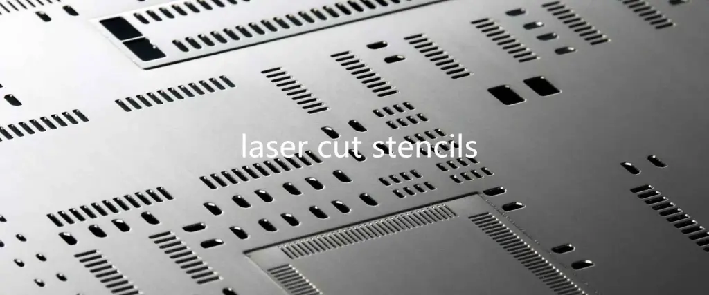
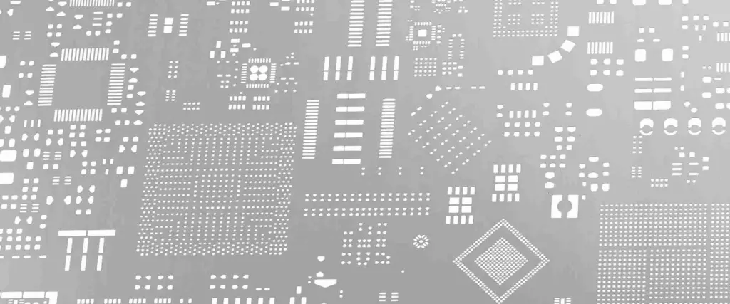
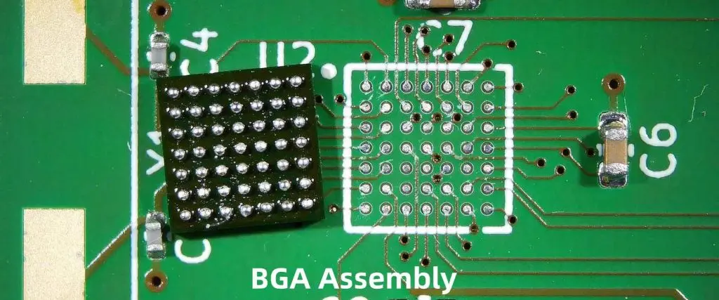
Stencils are used in the surface mount technology (SMT) assembly process to apply solder paste onto printed circuit boards (PCB) before component placement. The two main types of stencils used are laser cut stencils and etched stencils. This article compares these two stencil fabrication methods in terms of accuracy, speed, cost, durability, and other factors relevant to the SMT assembly process.
Overview of SMT Stencils
SMT stencils are thin metal sheets, usually made from stainless steel, that contain apertures or openings matching the pads and patterns on the PCB. Solder paste is applied over the stencil, then a squeegee blade is used to force paste through the openings onto the PCB. After stencil printing, components can be accurately placed onto the deposited solder paste.
Stencil Design Basics
Made from stainless steel foil, typically 100-250 μm thick
Laser systems offer much faster stencil fabrication time compared to chemical etching.
Laser cutting speed up to 100 mm/s
Typical stencil cutting time < 1 hour
Etching rates 10-25 μm/min vertically
Foil etching time 1.5 to 4 hours
Laser ~4-10x faster than etching
The slower etching process limits throughput. Lasers provide rapid turnaround which is advantageous for prototyping and short run stencil needs.
Stencil Durability and Lifetime
Laser cut steel stencils generally demonstrate better durability than etched versions.
Laser cut edges are clean and smooth
Etched stencils prone to foil burring on aperture walls
Burrs and jagged edges worsen during cleaning cycles
Laser stencils typically last 1.5-2x longer than etched
Laser produces less undercut than etching process
Undercuts enlarge over repeated use, reducing accuracy
Lasers produce cleanly sheared stencil walls without etching roughness. This improves paste release and cleaning while extending overall stencil lifetime.
Cost Analysis
Etched stencils have generally lower fabrication costs compared to laser cutting:
Etch resist materials cheaper than laser metal foils
Laser cutting equipment more expensive to purchase and operate than etching systems
Setup costs lower for etching artwork vs laser programs
Laser maintenance and gases add cost
Laser cutting costs ~20-40% more than etching
However, the extended lifetime of laser cut stencils offsets the higher initial cost over repeated production use.
Aperture Aspect Ratios
Laser cutting enables higher aspect ratio apertures than chemical etching:
Laser can cut 1:10 aspect ratios and beyond
Etch limits are around 1:5 aspect ratio
Tight process controls required for high etch ratios
Laser achieves finer pitch without aperture elongation
High aspect ratios allow thinner stencils to print small features. This helps improve solder paste release.
Design Flexibility
Laser systems provide greater design flexibility versus etching constraints:
Laser can cut any aperture size or shape
Etching limited to rectangular apertures
Laser achieves complex patterns not possible with etching
No risk of etch resist clogging fine features
Easier to make design adjustments with laser
Lasers enable innovative stencil geometries to optimize print performance and solder deposition.
This makes laser cutting a cleaner and more sustainable stencil production method.
Qualitative Comparison Summary
Table 2. Summary comparison of stencil fabrication methods
Parameter
Laser Cut
Etched
Accuracy/Resolution
Excellent
Moderate
Cutting/Etch Speed
Very Fast
Slow
Durability
High
Moderate
Cost
Moderate
Low
Aspect Ratio
High
Moderate
Design Flexibility
High
Low
Foil Options
Many
Few
Environmental Impact
Low
Moderate
Applications and Recommendations
When to Use Laser Cut Stencils
High density components < 0.5 mm pitch
Small apertures < 200 μm
Fine feature printing resolution < 100 μm
Complex aperture shapes required
Prototyping with short fabrication time
Ultra thin stencils <100 μm
Exotic foil materials needed
When Etched Stencils Are Acceptable
Pitch > 0.65 mm with std. apertures
Medium to large apertures > 300 μm
Cost-sensitive high volume production
Quick turnaround not essential
Environmentally safe etching available
Willing to accept reduced lifetime
Conclusion
Laser cut stencils offer superior accuracy and lifetime for fine pitch SMT printing. However, etched stencils can provide a lower cost option when resolution requirements are more relaxed. Characteristics of the target PCB, components, and solder paste should be evaluated to determine which fabrication method best suits the application needs. Both technologies continue improving, but laser cut stencils are expected to maintain advantages as electronics assemblies become progressively more miniaturized.
Frequently Asked Questions
What are the key advantages of laser cut stencils?
The main benefits of laser cut stencils are higher precision, faster fabrication, smoother aperture walls, greater durability, and broader material/design flexibility compared to etched stencils. This makes them ideal for high density SMT printing.
When is etching still a good option over laser cutting?
For less demanding applications with larger features (>300 μm) and lower cost sensitivity, etched stencils can be an acceptable alternative at a lower price point. But laser cut stencils outperform etching for fine pitch work.
What are typical laser cutting tolerances?
Precision laser cutting can reliably achieve ~25 μm accuracy and ±10 μm tolerance on stencil aperture dimensions down to at least 150 μm. Lasers can cut apertures smaller than 100 μm.
How many prints can be achieved with a laser cut vs. etched stencil?
Typical lifetime prints for a laser cut stencil exceeds 800, with some lasting 2000+. Etched stencils average around 500 prints before degradation impacts process capability.
Does laser cutting work with very thin stencil foils?
Yes, lasers have demonstrated good cutting quality with foils down to at least 25 μm thickness. Etching has more difficulty holding tolerances below 100 μm foil.
Shengyi PCB materials have proved to be very effective in fabricating printed circuit boards. However, there are several types of Shengyi PCB materials. In this article, we will be discussing Shengyi S1000 and its properties.
What is Shengyi S1000?
The Shengyi S1000 is a highly efficient laminate used for bonding several layers of multilayer boards. Also, it is an fr4 lead-free compatible laminate. The Shengyi S1000 is a PCB material that features several properties. Therefore, they are ideal for use in fabricating high performance PCB. This PCB raw material features great heat dissipation.
Shengyi S1000 PCB material has several features. These features are peculiar to Shengyi S1000.
Lead-free compatible
Shengyi S1000 laminate features lead-free compatibility. This means that it is compatible with lead-free laminate materials. Therefore, the Shengyi S1000 is very safe for use. Also, due to this great feature, it is environmentally friendly.
High heat resistance
Shengyi S100 is useful in high temperature applications. Also, this laminate has the ability to withstand extreme heat. It can dissipate heat properly.
With the Shengyi S1000, you can drill holes for mounting of components. This laminate enables PCB manufacturers to drill different sizes and types of holes in it.
Low water absorption rate
This is one of the greatest features of Shengyi S1000. It has the ability to withstand water. Therefore, this laminate can function well in a humid environment. Also, the moisture absorption of Shengyi S1000 is 0.09%.
Excellent thermal reliability
This laminate is thermally stable when used at various temperatures. Thermal reliability refers to the ability of a material to remain stable when exposed to high temperatures. Shengyi S1000 features great thermal reliability. Therefore, this laminate is ideal for use in varying temperature ranges.
High Tg
Shengyi S1000 PCB material features a high glass transition temperature. Also, the Tg of this PCB raw material is 155 degree Celsius.
UV blocking
Another great feature of Shengyi S1000 PCB raw material is its ability to block the effect of UV rays.
High Decomposition temperature
The decomposition temperature (Td) refers to the temperature at which a PCB material decomposes chemically. Shengyi S1000 has a high decomposition temperature. The Td is 335 degree Celsius.
Shengyi S1000 is ideal for use in a wide range of applications.
Computer and communication equipment
Shengyi S1000 laminate is useful in the production of communication equipment like cell phones and computers. Also, this laminate features excellent thermal reliability and high heat resistance. Most times, computers work under high temperatures. Therefore, this laminate protects these devices from overheating. Overheating can result in circuit failure.
The Shengyi S1000 is widely used in the automotive industry. You can find this laminate in automobiles. Also, it enhances the functionality of the automobile features. This laminate is very effective in designing automobile parts.
Instrumentation
Shengyi S1000 is a PCB material useful for designing several types of equipment and instruments. You will find this laminate in sensors. Shengyi S1000 helps to improve the design of this equipment and instrument.
The Significance of Glass Transition Temperature (Tg) on Shengyi S1000
The glass transition temperature describes how a PCB material transforms from a solid state to a molten state. Shengyi S1000 features a glass transition temperature of 155 degree Celsius. Therefore, this PCB material will be unstable once it works beyond 155 degrees Celsius. This Tg value helps to determine the limit of temperature operation.
Also, it is important to stay below 155 degrees Celsius to maintain the stability of this material. Tg is important in determining the higher temperature limit for the use of solid materials. Also, this property helps to optimize production parameters. Therefore, glass temperature is ideal for failure analysis and quality analysis.
Higher Tg guarantees the thermal stability of a material. A Tg of 155 degree Celsius is considered a high Tg. There are different ways to test the Tg of Shengyi S1000. These techniques are dynamic mechanical analysis and thermal mechanical analysis. Also, you can use the differential scanning calorimetry.
However, there are some factors that affect the Tg of a material at 155 degree Celsius. For instance, the chemical structure of the materials can affect Tg. A Tg at 155 degree Celsius has its own advantage. The Shengyi S1000 features a low thermal expansion due to its Tg.
Properties to Consider When Opting for Shengyi S1000
There are different types of Shengyi products available. It is important to understand the properties of the Shengyi S1000 laminate. This will help you determine if it meets the requirement of the intended application. Therefore, what properties should you put into consideration when choosing the Shengyi S1000?
Thermal properties
You need to consider the thermal properties of this laminate. Also, ensure it meets the thermal demands of the intended application. Consider thermal properties like flammability and thermal stress. Also, you should determine the minimum and maximum temperature limits of the Shengyi S1000. In addition, you need to consider the coefficient of thermal expansion.
Dielectric properties
Also, you should consider these properties. You will have to evaluate the dielectric properties of Shengyi S1000. These properties include dielectric strength and dielectric constants. Also, you need to determine the dielectric limits of this PCB material. Ensure it meets the dielectric demands of the intended application.
Volume and surface resistivity
These are important properties to put into consideration when choosing the Shengyi S1000 laminate. The volume and surface resistivity of Shengyi laminates differ. Shengyi S1000 must meet the volume and surface resistivity demands of your application. Therefore, specify the maximum surface and volume resistivity based on your application demands.
Temperature tolerance
The temperature tolerance talks about the decomposition temperature and glass transition temperature. The glass transition temperature of Shengyi S1000 is 155 degree Celsius. Also, this laminate has a decomposition temperature of 335 degree Celsius. Ensure the temperature tolerance of Shengyi S1000 meets the temperature demands of your application.
Conclusion
Shengyi S1000 is a lead-free compatible laminate ideal for use in a wide range of applications. This laminate features great thermal and mechanical properties. We have discussed important details on Shengyi S1000 in this article.
Arlon (formally known as Arlon Industries) is a leading manufacturer of U.S.-based linens and other textiles. One of the newest and most popular products is their Arlon 35n. They specifically meet all the demands of today’s commercial laundry facilities. They also offer exceptional energy savings with bottom-line benefits apparent right away.
Arlon 35n Properties and Specifications
First, just a brief overview of the product itself since this is an area where there can be some confusion. The Arlon 35n is a new fabric derived from combining woven fabrics. They create a high-density, high-absorption fabric with an extremely soft feel. We’ll go into more detail below. However, this product line is different. It offers both water absorption and dryer energy savings. At the same time, it maintains exceptional flexibility and durability. Additionally, it can absorb up to 170% more water and still provide the same level of softness as traditional fabrics.
All the benefits of this product line begin with the fact that it’s created from 100% spun-bond material. It is a highly durable and flexible product that offers exceptional softness and flexibility. These factors are essential to keep in mind. They ensure that your linens maintain their durability and absorbency for as long as possible. So naturally, this is also a product line that includes the other benefits you’d expect from a spun-bond product. They include high energy savings, low linting levels, stain resistance, and softness. Again, this is unlike anything previously available in the industry.
For these reasons above all others, Arlon 35n has is an excellent product used by Rayming PCB & Assembly.
Each Arlon product line has been created around specific categories. So, users can get precisely what they need for their laundry requirements. Fortunately, the Arlon 35n is no exception. This fabric consists of a unique blend of spun-bond material and superabsorbent polymers. So, each category offers several different performance levels and optimized cost structures. Unfortunately, one of the minor drawbacks of this system is that it’s impossible to customize the different categories. This is because they offer only four basic levels.
1. Polymer:
This is the core of Arlon 35n performance and is one of the biggest areas where this product line can make a real difference. This coating consists of environmentally friendly materials. As a result, these materials last longer than any other similar product. In addition, this polymer coating can absorb 170% more water than similar fabric types. It means it performs better, dries faster, and absorbs more water in all possible applications.
2. Thermoset
Thermoset coating is suitable for bathrooms, and water touches the fabric anywhere. We can find this material in any Arlon product line. Still, it’s only offered in those areas where temperatures reach between 60° F and 80° F. This ensures that you have plenty of time to use your existing appliances before replacing them with more energy-efficient models.
3. Polyimide:
This very strong and durable material provides exceptional durability for laundry processes. The benefits of this type include the fact that it’s super resistant to stains and lint. In addition, it means you’ll be able to save money by replacing your current drying equipment in the future. It also offers superb water absorption and dryer performance, which means it can absorb up to 170% more water than traditional fabrics.
4. TS:
This is the softest type of fabric offered by Arlon, and it’s also one of their most popular. This material offers exceptional softness, but it can only absorb up to 50% more water than traditional fabrics.
This is certainly not a product line for high heat drying processes or even those that involve chemicals. However, the fact that it’s 100% spun-bond means these fabrics don’t tend to fray or shrink. If this sounds like what you need for your business, you should know that many different benefits are available from investing in Arlon 35n products.
The biggest advantage of investing in Arlon 35n products is its product line that blends exceptional cleaning and drying performance with enhanced durability. This is a patented technology designed using only the most durable materials. It means your linens will absorb more water than traditional spun-bond fabrics. This means you’ll have fewer issues with shrinking, fraying, and shrinkage. However, your linens will remain soft, bright, and absorbent for years.
2. High-temperature material
Another big advantage to investing in Arlon 35n fabrics is that they are suitable for heat. This means you can get faster and more effective drying times, resulting in much less time spent in the laundry room. As a result, this product line is an excellent choice for laundromat owners and those with commercial dryers at their disposal.
3. Easy to use
Arlon 35n fabric is just easy to use in every possible application when it comes down to it. Whether you’re working with fabric or sheeting, you’ll find that these products are extremely durable and absorbent. Thanks to the polymer coating on each strand of fabric.
Physical Properties
Density: It has 1.6g/cc. As mentioned earlier, this is lighter than average, and that’s because it’s spun-bond.
Water absorption: 0.26% more water-absorbent than traditional materials. As mentioned earlier, this isn’t particularly important in the case of linens since they always help in washing machines. This figure is interesting because it’s relevant to anyone making towels and bedsheets.
Mechanical Properties
Peel Strength: It has 3500 mm/min. This is decent for a woven, but it’s poor for a spun-bond.
Poissons Ratio: This is 0.12 and is good for spun-bond fabrics but much better than the 0.06 you might expect otherwise.
Tensile Strength: It has 21N/mm2, which is poor for a high-performance fabric. It’s about what you’d expect from a high-performance woven, though (and about 10x better than PTFE).
Modulus of Elasticity: It has 1500 mm, which is pretty good for a spun-bond and much better than a typical woven fabric.
Arc Resistance: Not tested, but it is polypropylene, so it should have decent arc resistance.
Dielectric Strength: Not tested, but it is polypropylene, so it should be pretty good for its density.
Volume Resistivity: Not sure how to test this one. For instance, how much it resists the electric field in the material and thus the electric current through the water. However, judging from its crystalline structure, I guess it’s about the same as PTFE.
Dissipation Factor at 1kHz: This is 0.00016, which is poor and only 12% of PTFE’s 0.
Dielectric Constant: This is 1.65, which is better for polypropylene than polyethylene 1.
Thermal Properties
Coefficient of Linear Expansion: Not sure how to test this one.
Heat Distortion Temperature: Not sure how to test this one.
Glass Transition Temperature: This is 48 °C, just like PTFE, which means it might be a usable alternative to PTFE if you can get the cost down.
Melting Point: This is 264 °C. The shear strength will be a problem at temperatures above ~260 °C. However, it’s still valuable for laundry and might be helpful in smaller applications.
Conclusion
This is a promising material and could help in specialized areas where a nonstick surface is needed, but it’s too expensive to replace PTFE.
The first thing to understand about the nonwoven business is that the market for spun-bond products is huge. That isn’t to say they’re all sold to consumers. Instead, most are sold as industrial fabrics or as materials for lower-end clothing items like underwear and leisurewear.
If you decide to work with this product line, you need to know about numerous different types of spun-bond.
The FR3 PCB is a circuit board design program that’s affordable, intuitive, and versatile enough for beginners and professional designers. The main benefits of this program include its high level of compatibility. It also consists of the low cost of the software licenses, an extensive library, and full editing capabilities in vector format. The FR3 also allows users to create custom libraries that we can share using this software. It is perfect for those who want to take their PC board layout skills to the next level.
Although these programs are very similar, they have significant differences that set them apart. The FR3 software is more comprehensive and user-friendly than the Eagle software, but it comes at a much higher cost. It also allows unlimited polygons and tracks with a low polygon count of 5,000 and a track count of 10,000 per board. While the Eagle software has a lower polygon count at 4,900 and a lower track count at 8,000 per board. However, their differences do not end there. The most apparent difference between the programs is each product’s license costs.
FR4 is the FR3 PCB’s later successor. The significant difference between the two programs is that FR4 comes with more and better features than FR3. It has an enhanced interface and better usability, with a less complex learning curve. In addition, the program allows easier routing capabilities when users want to achieve their final design. It also contains a helpful and extensive library with symbols, footprints, and templates that users can use in their designs.
The FR4 software has many advantages over the FR3 PCB, but it also has shortcomings. The main disadvantage of the FR4 is that it only supports four layers and a total design size of 8.27 inches by 11 inches. Another drawback is that there are no designated libraries for FR4. Although, beneficial symbols and footprints are in this website’s library section. Lastly, the program only allows a maximum polygon count of 3,000 polygons and a maximum track count of 6,000 tracks per board.
The best advice anyone can give regarding these programs is to try using both. Do this before deciding what you would like to use professionally or recreationally in your projects.
1. Glass-reinforced phenolic (FR-4) substrate with pre-molded copper cladding. This provides ease of manufacture, mechanical stability and durability, excellent track density capability, and low cost.
2. Copper capped alumina substrate (FPAK) is an alternative to GF material. We use them for high-temperature applications or where arcing is a problem. FPAK provides excellent thermal conduction. In addition, it allows for increased current carrying capacity compared to standard FR4 material.
3. We can use single-sided glass laminate (SGLA) with low power boards. This requires extra strength and protection from moisture or corrosive atmosphere. Examples include automotive or industrial applications.
4. Non-conductive epoxy resin (NCER) is helpful for areas where we cannot use conductive traces. Examples include connectors and through-hole vias.
5. We use Pressure-sensitive adhesive (PSA) for attaching parts, for example, ICs, to the PCB.
6. Electroless nickel immersion gold and chemical/mechanical polishing achieve surface finish within or beyond 25 µin.
7. Pre-punched paper tape helps hold down components during the assembly of the PCB. We can dispense it from press-fit machines directly onto the PCB surface. We do not need any additional adhesive.
FR3 PCBs are one layer (1-layer) to eight layers (8-layer).
We can manufacture the FR3 PCB in single or double-sided versions.
The FR3 PCB is a one-sided technique. It uses a copper-clad substrate with two or more layers of copper foil laminated onto each side of the substrate.
We etch the traces on the substrate, and then we remove the copper from all but the required layers. Next, we create ground planes by etching away all exposed copper between the required traces leaving isolated ground areas where needed. Through-hole plated holes allow for mounting components and surface-mounted devices.
CAD Design
The CAD package used to produce the FR3 PCB is Eagle PCB Editor. The PCB copper foil or copper cladding consists of 35μm and 163μm thickness material. The FR3 PCB has a maximum line width of 2.5 µm and minimum line width of 0.15 µm (15 mils).
The FR3 PCB can have up to three levels of hierarchy in its design: board, layer, and track level. This allows the minimum number of total tracks on the board to be 8 for multilayer pcb boards with no vias. Ground planes are essential for all signal layers except for signal layer number six. It may not contain any ground plane.
Best ways to drill holes in FR3
We can achieve drilling the FR3 PCB in several ways. First, through-hole drilling using hand tools is usually suitable for PCBs with through-hole vias.
PCB thickness can vary from 0.8mm for single-layer boards to 1mm for double-layer boards.
Through-hole vias must be straight and vertical to provide maximum trace clearance. Unfortunately, this gives rise to two problems when drilling holes in FR3 PCBs with through-hole vias.
Drill bit contact
Increased resistance to vibration
a) Mechanical drilling:
We must use a drill bit with a larger diameter to prevent the bit from binding in the smaller hole. This will increase resistance to vibrations. Drill motors are available specifically for drilling through holes in FR3 PCBs. They do not require an additional threaded insert. However, these can cost up to $200 each.
b) Laser drilling:
A laser cutter is a great way to make straight-through holes in FR3 PCBs. The cutters can create 0.5mm holes within a 0.25mm hole, resulting in minimal clearance from the drill bit to the FR3 PCB surface. This increases drilling resistance and vibration. We can minimize it by using an oscillating hand drill on FR3 PCBs with through-hole vias or ground planes.
c) Drill bits:
We can order drill bits for 14 and 16 gauge HSS drills from McMaster-Carr or Mouser Electronics for $100 each. Cheaper options are available if several holes need drilling to accommodate through-hole vias.
The FR3 PCB is essential in various applications in the electronics industry. However, it is also applicable to many applications that require high strength, ease of assembly, and small size.
Electronics:
The FR3 PCB is helpful as the board material in motherboards, consumer-level computers, and mobile devices.
Automotive:
The FR3 PCB can be helpful in automotive applications because of its low cost, durability, and reliability. In addition, it is helpful to any auto parts manufacturer that needs to manufacture small batches with minimal lead time.
Automotive applications of the FR3 PCB include:
a) Instrument clusters display vehicle information such as speed, RPM, and other valuable metrics. Applications include the dashboard, center counsel, and in-vehicle entertainment (IVI) systems.
b) Power supply modules, which we can integrate with other modules or build into compatible devices. Examples include airbags and ABS sensors, and we use them for automotive purposes. This allows you to install circuit boards with specific functions in any number of locations inside the vehicle. You do not need to change any wiring or software changes.
Industrial:
The FR3 PCB is helpful in high-performance, highly reliable industrial applications. Examples include computer-controlled instruments and sensing devices.
Electronic or electromechanical sensors are usually installed on the boards and connected to external equipment through wires. These are inside various housings, such as extruded aluminum housing, to ensure the board has no contact with air.
The FR3 PCB can also be essential for in-vehicle electronics. It makes it easy for Rayming PCB & Assembly to create new electrical and electronic systems quickly.
Others:
RFID tags are commonly mounted onto FR2 PCBs. We then transfer it onto their final application using an adhesive that adheres to the FR3 PCB tag. These are generally 0.5 to 2mm thick.
Conclusion
FR3 PCBs are inexpensive, more rigid, and stronger than FR1 PCBs. As a result, they provide a low-cost and reliable board alternative to aluminum PCBs. In addition, FR3 PCBs are lighter, take up less space, and we can manufacture them faster than FR4 PCBs.
The FR3 PCB has a wide variety of applications in the electronics industry, ranging from video games to mobile devices.
FR3 is not helpful for every application because of its rigidness and low thermal conductivity properties. However, it is a board with many unique properties that professionals can utilize.
Electrostatic discharge (ESD) refers to the sudden flow of electricity between two electrically charged objects caused by contact, an electrical short, or dielectric breakdown. ESD can cause serious damage to electronic equipment and components. The rapid transfer of electrostatic charge can result in a short but high current flow that can melt metal surfaces or puncture insulating materials. ESD is a concern in many industries that rely on electronics and integrated circuits, such as aerospace, automotive, medical devices, and electronics manufacturing.
Key Facts About ESD
ESD is caused by an imbalance of electric charges between two objects. This imbalance creates an electric field.
When the two objects make contact or approach very close together, electrons transfer rapidly to balance the charges.
The transfer of electrons in a short burst creates the ESD event.
ESD can happen through direct contact or via induced electric fields.
ESD typically occurs at voltages below 15,000 volts.
The discharge usually lasts for just a few nanoseconds.
ESD can generate currents of more than 1 ampere.
The associated power levels can melt metal surfaces or vaporize materials.
ESD Damage Mechanisms
ESD can damage electronic components and devices in several ways:
Thermal damage – High currents can cause localized overheating, which can melt metal interconnects or fuses.
Vaporization – Insulating layers can be “punctured” by ESD, allowing metal migration that creates short circuits.
Gate oxide breakdown – Thin insulating films inside ICs can be ruptured by ESD.
Latch-up – Parasitic circuits triggered by ESD can disrupt normal functioning.
Signal errors – Fast transients can alter logic states or stored data.
ESD Standards
There are several important standards that provide testing methods and ESD control recommendations:
ANSI/ESD S20.20 – For the Development of an Electrostatic Discharge Control Program
IEC 61340-5-1 – Protection of Electronic Devices from Electrostatic Phenomena – General Requirements
JEDEC JESD22-A115 – Electrostatic Discharge Sensitivity Testing Human Body Model (HBM) Component Level
IPC-A-610 – Acceptability of Electronic Assemblies
IPC 7711/7721 – Rework, Modification and Repair of Electronic Assemblies
These standards help define appropriate ESD control procedures and requirements for electronic components and assemblies.
ESD is fundamentally caused by the build up and discharge of static electricity. Certain materials like plastics and fabrics tend to gain and hold significant static electric charges more easily. ESD occurs most commonly under conditions of low humidity, which reduces conductivity and the natural dissipation of static charges. There are two primary modes of ESD – directly contact discharge and induced air discharge.
Contact Discharge
Contact discharge occurs when two objects come into direct contact while having substantially different electrostatic potentials. For example, an integrated circuit (IC) slid across a table surface can transfer charge due to rubbing contact. If the acquired charge on the IC is of opposite polarity to a nearby grounded point, a rapid ESD event can occur when they make contact. The discharge may happen through a single pin or lead of the IC package.
Induced Air Discharge
Air discharge ESD happens when an object with high electrostatic charge comes close to a conductive object at a different potential without actually touching it. The strong electric field gradients that form around the charged object induce currents that can arc across the air gap. Sparks are a common example of air discharge ESD. This frequently occurs as someone walks across a carpet on a dry day and then approaches a grounded metal object like a door knob or file cabinet.
Triboelectric Charging
Many common materials can acquire significant static electric charges through a process called triboelectric charging. This involves charge transfer between two surfaces during rubbing contact. Some examples of materials that readily gain charge this way include:
Plastics – PET, PVC, polystyrene, polyethylene
Paper products
Glass
Synthetic fabrics and textiles
Charge build up is affected by properties like surface roughness, conductivity, and chemical characteristics. Generally, rubbing dissimilar materials produces greater static charging than similar materials.
Electrostatic Induction
Electrostatic induction describes how electric charges can influence the distribution of charges in nearby conductive objects without physical contact. When a charged object is brought near an uncharged conductor, electrons in the conductor will shift position. For example, proximity to a negatively charged object will repel electrons in the conductor, leaving the facing side with a net positive charge. This induced polarization effect can facilitate ESD when the two objects are grounded at different times.
ESD Effects on Electronics
ESD can cause both immediate and latent damage to electronic components and assemblies. Sensitive components need to be handled carefully using ESD protection techniques to prevent harmful discharges. Some key effects of ESD on electronics are highlighted below.
Latch-Up
Latch-up occurs when parasitic circuit elements trigger a high current state that disrupts normal operation. ESD can activate p-n-p-n junctions inherent in CMOS ICs to initiate latch-up and potential thermal runaway. Latch-up may cause the device to stop functioning until power is cycled. Repeated latch-up can degrade reliability over time.
Gate Oxide Breakdown
The thin insulating gate oxides of MOSFET transistors can be ruptured by ESD. Gate oxide puncturing leads to short circuits and improper operation. Oxide breakdown is a common ESD failure mechanism in integrated circuits.
Junction Damage
Forward and reverse biased PN junctions are subject to damage at high ESD currents. Thermal effects can melt silicon and metallization, altering device characteristics. ESD protection circuits help clamp junction voltages during ESD events.
Metallization Burnout
Conductors and interconnects can melt, vaporize, or migrate when subjected to brief, high current ESD pulses. Thin metal semiconductor contacts and wire bonds are especially susceptible. This can create open circuits within ICs.
Passivation Cracking
The insulating passivation layers on chips can crack under ESD stress. Cracks expose the silicon and traces to contaminants and moisture that can lead to corrosion over time and eventual circuit failure.
Dielectric Breakdown
Insulating films between metal layers can breakdown during ESD events, leading to shorts between traces. This damages circuit functionality through parasitic conduction paths.
ESD Sensitive Components
Many types of electronic components and devices are susceptible to ESD induced failure and damage:
To adequately protect components and products from ESD damage, manufacturers implement structured ESD control programs. These institutionalize best practices for handling, storage, packaging, and assembly operations.
The ANSI/ESD S20.20 standard covers key requirements for developing, implementing, and monitoring an ESD control program. It establishes ESD program fundamentals including:
Grounding/Equipotential bonding systems
Personnel grounding
ESD protected areas (EPAs)
ESD sensitive devices (ESDS) handling
Compliance verification
Adhering to S20.20 ensures all necessary aspects of ESD control are addressed. Many electronics companies mandate compliance with this standard.
ESD Control Handbook
The ESD Control Handbook from the ESD Association provides in-depth guidance on all aspects of ESD control in electronics manufacturing and handling. Topics covered include:
ESD basics and testing
ESD program management
Facilities and equipment grounding
EPA requirements
Packaging, storage, and handling
Training techniques
Compliance verification
ESD Protective Equipment
A variety of specialized equipment helps protect electronics from ESD damage during manufacturing, assembly, test, inspection, and storage operations.
Workstation Equipment
Wrist Straps – Ground personnel through a coiled wire and resistor. Used when handling ESD sensitive items.
Footwear Straps – Conductive shoes or heel straps for personnel grounding.
Floor Mats – Dissipate charges from personnel at workstations.
Table Mats – Dissipative surfaces for work areas.
Garments – ESD protective smocks, coats, and finger cots.
Workplace Fixtures
Shelves and Racks – Metal units for grounded storage.
Carts and Carriers – Mobile grounded platforms for WIP transport.
Ionizers – Charge neutralization for workspaces and tools.
Testers – Devices to check grounding integrity.
Component Handling
Tweezers – ESD safe versions with conductive tips.
Meters – Handheld and benchtop monitors to check electrostatic levels.
Instrumentation – Data logging systems for continuous monitoring.
Testing – Simulators and generators to test ESD susceptibility.
ESD Standards and Models
Human Body Model
The Human Body Model (HBM) represents ESD events caused by human contact. It consists of a 100 pF capacitor discharged through a switching component and 1.5k Ω series resistor into the device under test. This models the capacitance of the human body and skin resistance. HBM testing per JEDEC JESD22-A115 evaluates component sensitivity levels.
Machine Model
The Machine Model represents discharges from equipment through metal conductors or charged insulators. A 200 pF capacitor is discharged directly into the device, producing higher peak currents than HBM. Machine Model testing per IEC 61340-3-1 and ANSI/ESDA S5.2 characterizes robustness for automated handling.
Charged Device Model
The Charged Device Model (CDM) evaluates susceptibility when a device itself becomes charged and then discharges to ground. For CDM testing, the device is charged with a high voltage supply before being discharged through a current limiting resistor. JEDEC JESD22-C101 defines standard CDM testing.
IEC 61000-4-2 Air Discharge
IEC 61000-4-2 simulates ESD events generated through air discharge to product enclosures and housings. It utilizes higher voltages and currents than other ESD models. This technique assesses robustness for end-use conditions.
ESD Failure Analysis
When an ESD-related failure occurs, a structured analysis helps identify the root cause and point of weakness. This drives corrective actions and improvements to prevent similar issues going forward.
Gather Information
When/where did failure occur?
What was procedure being performed?
What equipment was involved?
Was established ESD protocol followed?
Visually Examine
Use stereo zoom microscopes to inspect.
Look for physical damage like burns, pits, cracks, melted regions.
Note location of damage on device.
Electrical Testing
Perform in-circuit tests to isolate faults.
Power-up devices and monitor current draw.
Logically exercise IC pins and trace connections.
Imaging Techniques
Take high magnification photos of damage areas.
Use scanning electron microscopy for detailed images.
Perform x-rays and thermal imaging.
Physical Analysis
Cross-section damaged components.
Use FIB-SEM to see failure origins.
Execute EDX and EELS to identify contamination.
Simulate ESD
Reproduce suspected ESD event on samples.
Observe effects under controlled conditions.
ESD Design Strategies
Circuit designers utilize various strategies to make devices more robust against the effects of ESD:
Protection diodes – Adds diodes to clamp pin voltages during ESD.
Guard rings – Routes conductive rings around I/O pins on the silicon die to steer current from ESD strikes.
Snapback devices – SCRs and BJTs that enter snapback mode to shunt ESD current.
Rail clamps – Shunts power rails to ground during overvoltage from ESD.
Internal ESD diodes – Adds parasitic diode structures between pins to bypass ESD current.
Series resistance – Resistors limit input current to sensitive nodes during ESD.
Current ballasting – Adds distributed resistance in output drivers to limit current per pin.
Emitter ballasting – Inserts individual emitter resistors in parallel transistors to balance ESD currents.
Silicon-Controlled Rectifiers (SCRs) – Turns on during ESD to shortcut input to ground or power rail.
Device spacing – Separates transistors and routing to reduce risk of shorts from ESD damage.
ESD Risk Management in Manufacturing
Several strategies can reduce ESD risks during manufacturing operations:
Assign an ESD program coordinator
Follow ANSI/ESD S20.20 requirements
Provide comprehensive ESD awareness training
Establish ESD protected areas (EPAs)
Use wrist straps, footwear straps, and mats at EPAs
Apply ESD protective packaging for WIP and storage
Ground all equipment, carts, and fixtures
Utilize ionization to neutralize charges
Monitor EPAs for electrostatic discharge events
Perform regular testing to qualify EPAs
Conduct internal ESD audits and tracking
Include ESD requirements in supplier agreements
Label ESD sensitive components and assemblies
Document ESD protocols and procedures
ESD Risk Analysis
Identify activities that can generate electrostatic charge
Determine which materials and processes are high risk
Evaluate component and product ESD sensitivity levels
Assess which personnel roles and operations pose highest ESD risks
Maintain records of ESD events and associated failures
Periodically analyze ESD risks based on data and experience
ESD Mitigation Strategies
Substitute high charging materials with dissipative or grounded versions
Increase humidification levels in EPAs
Reduce unnecessary movement of items
Use static neutralizing ionization blowers
Improve EPA layouts to limit charge buildup
Implement more frequent grounding procedures
Enforce rigorous wrist strap testing and auditing
ESD Protection in Device Packaging
Packaging and handling procedures safeguard electronic components and assemblies during transport and storage. Key aspects include:
Shielding Bags
Metallized polymer bags encapsulate devices to isolate them from electrostatic charges. Bags meet shielding effectiveness requirements of standards such as MIL-STD-129 and ANSI/ESD S541.
Conductive Foam and Film
Components are cushioned and separated from charges using conductive polyethylene foam or plastic film inserts and liners inside packaging. This also prevents device charging.
Anti-Static Shipping Tubes
Rigid conductive tubes provide protection for larger items such as circuit boards during handling and shipping. The tubes connect electrically to the contents.
Groundable Materials
ESD safe packaging utilizes static-dissipative and electrically conductive materials. This prevents charge accumulation on packages.
Warning Labels
Labels indicating ESD sensitive contents remind personnel to follow proper ESD handling procedures when interacting with the packaged components.
Moisture Barrier Bags
Separate moisture barrier bags are used to prevent humidity related corrosion during longer term component storage. Desiccants are also added in some cases.
Stackable Configuration
Packaging allows charged devices to be stacked vertically without contacting each other. This reduces ESD risks during transportation stacking.
ESD prevention in PCB assembly
Printed circuit board (PCB) manufacturing and assembly is an ESD-critical application. Bare PCBs contain highly sensitive components and traces. Proper ESD protocols must be followed throughout PCB population, soldering, test, inspection, and repair.
ESD Protection Guidelines
Use wrist straps, heel straps, and conductive flooring in assembly areas
Keep workstation grounds properly connected
Utilize ionizers to neutralize electrostatic charges
Handle PCBs by the edges only
Store PCBs in anti-static bags or boxes when not being processed
Avoid touching component pins or landings on bare boards
Place PCBs PCB-side down onto grounded assembly worksurfaces
Keep assembly materials (e.g. solder) in grounded containers
Ensure all equipment like soldering irons are grounded
Exercise caution when removing PCBs from bags
Avoid rapid motions that may generate charge
Only assemble PCBs in designated ESD-controlled areas
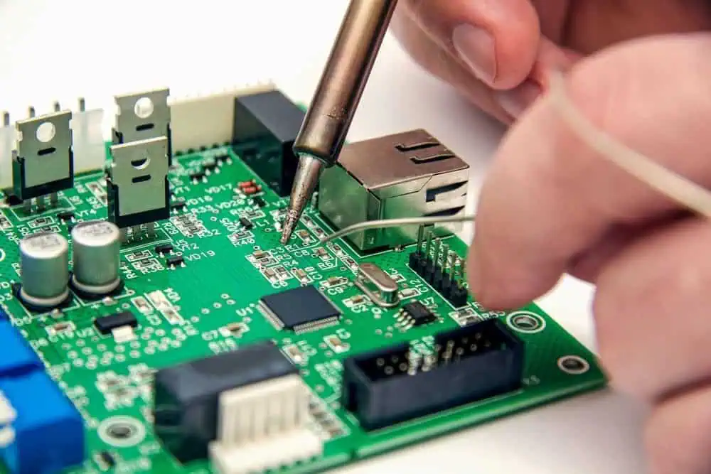
Electronic devices are an important part of present life since they have a wide range of applications. However, the existence of these devices solely depends on electronic assembly. For example, the manufacture of such appliances like refrigerators, smart cars, air conditioners, and many other machines depends on printed circuit boards (PCBs). Therefore, we will look at what electronic assembly at home is and dig deep into what it involves. In addition, we will highlight the advantages and disadvantages of assembling electronics at home.
What is Electronic Assembly at Home?
Understanding the Concept
Electronic Assembly at Home refers to the process of assembling, soldering, and testing electronic components and circuit boards in a residential setting. This practice has gained popularity due to advancements in technology, the rise of the maker movement, and the increasing demand for flexible work arrangements.
Typical Tasks Involved
When engaging in electronic assembly at home, you can expect to perform a variety of tasks, including:
Effective communication with clients and team members remotely
Keeping up with rapidly evolving technology and techniques
Tips for Success in Home-Based Electronic Assembly
To thrive in the world of electronic assembly at home, consider these tips:
Building a Professional Home Workspace
Dedicate a specific area for your electronic assembly work
Invest in proper lighting, ventilation, and ergonomic furniture
Organize your tools and components for maximum efficiency
Continuous Learning and Certifications
Pursue industry-recognized certifications like IPC-A-610
Attend online workshops and webinars to stay updated on new technologies
Experiment with different types of projects to broaden your skill set
Keeping Up with Technology Trends
Subscribe to electronics and maker-focused publications
Join online communities and forums to exchange knowledge
Explore emerging technologies like IoT and wearable electronics
Best Practices for Quality Assurance
Develop a systematic approach to testing and inspection
Document your processes and create checklists for consistency
Invest in quality tools and equipment for reliable results
Resources for Learning and Improving Your Skills
To continue growing in the field of electronic assembly, take advantage of these resources:
Recommended Online Courses and Tutorials
Coursera’s “Introduction to Electronics” by Georgia Tech
edX’s “Electronic Interfaces: Bridging the Physical and Digital Worlds” by UC Berkeley
Udemy’s “Learn to Solder: Electronics Soldering for Beginners”
Community Forums and Maker Spaces
Join local maker spaces or hackerspaces for hands-on learning
Participate in electronics forums like EEVblog or All About Circuits
Attend maker faires and electronics expos to connect with like-minded enthusiasts
Useful YouTube Channels, Blogs, and Certifications
YouTube channels: EEVblog, GreatScott!, and AdaFruit Industries
Blogs: Hackaday, Electronics-Lab, and SparkFun
Certifications: IPC-A-610 (Acceptability of Electronic Assemblies), J-STD-001 (Requirements for Soldered Electrical and Electronic Assemblies)
Conclusion
Electronic Assembly at Home presents a wealth of opportunities for both hobbyists and professionals alike. From mastering PCB soldering techniques to assembling complex circuit boards, the skills you develop can lead to fulfilling work-from-home jobs and entrepreneurial ventures.
As you embark on your journey in electronic assembly, remember that success comes with practice, continuous learning, and attention to detail. Whether you’re just starting or looking to expand your existing skills, the world of electronic assembly at home offers a pathway to creative expression, technical mastery, and professional growth.
By following the guidelines, tips, and resources outlined in this article, you’ll be well-equipped to transform your passion for electronics into a rewarding home-based career. Embrace the challenges, stay curious, and never stop learning – the future of electronic assembly is bright, and it starts right in your own home.
When it comes to lead free compatible laminate for circuit boards, the Shengyi Synamic 6N PCB is one to trust. This laminate is the type that can hold up a multilayer PCB board without any barrier.
The Shengyi Synamic 6N is highly durable and has many features that make designers and engineers use it for their circuit boards. Also, this laminate is applicable in many areas which make it a very useful and reliable type of laminate.
In this article, you shall learn more about the Shengyi Synamic 6N PCB and how best it can work.
If you are familiar with circuit boards, you get to know that they cannot function without strong laminates. The Shengyi Synamic 6N is a type of laminate that holds up layers in circuit boards. Mostly, one uses it for multilayers in the PCB.
This laminate has the propensity for high performance in the Printed Wiring Board, PWB. Hence, this laminate works for any high speed digital appliances which demand maximal electrical conduct. This electrical conduct is nearly 50 Gbs+.
This PPE system can work effectively because of its high glass transition temperature. Accordingly, this is why it operates smoothly in HSD applications. Also, this laminate comes with both mechanical and electrical properties that are reliable.
The Shengyi Synamic 6N has exceptional PCB processability. This PCB laminate is resistant to heat. Therefore, no damage can occur as a result of any exposure to high temperature or heat. So, this type of laminate belongs to the low loss group.
Which Areas Can You Apply The Shengyi Synamic 6N PCB Material?
This is one of the frequently asked questions when it comes to Shengyi Synamic 6N. Then, it is because of how potent this PCB laminate is. Note that, you don’t have to worry about its lifespan when you use it. It can connect every layer on the circuit board for years despite its exposure to heat or harsh weather.
As a result of this, it becomes applicable in various fields or industries where you need the circuit board for your devices or applications.
High Performance Computing Device
This is one of the applications where you need Shengyi Synamic 6N PCB for. So, it is useful for high performance computers. These days, you can easily have access to computers whose performance is high. As long as you have this laminate present in the bonding of the circuit board, it works very fast.
Optical Communication Services
This is interesting because every optical communication application requires the Shengyi Synamic 6N. So, it helps the processing become easier and faster. You use it for optical fiber, signal lamps, optical communication that is free space, and photophone.
Accordingly, it helps manufacturers or engineers with their design in networking in any passive optical communication services.
Fast Data Processing
This PCB laminate is applicable in the world of fast data processing. Any data passing through the internet can become faster once the Shengyi Synamic 6N is used in routers. On account of this, it is applicable in switch, server, and storage.
HSD Networking Tools
For any high speed digital equipment, the Shengyi Synamic 6N PCB works effectively for it. You see it in interfaces such as DisplayPort, HDMI, Ethernet, and PCIe.
What are The Features of The Shengyi Synamic 6N PCB Material?
It is vital you know about the features of this laminate. With every laminate, each has its unique characteristics. Sometimes, they may be similar in functions. However, these laminates have varying levels of thermal reliability and water absorption.
Exceptional Thermal Reliability
This is one of the numerous features of the Shengyi Synamic 6N PCB. It has the ability to retain its stability under high temperature. This implies that this laminate is not affected by heat throughout its lifespan. Its thermal property makes it applicable to circuit boards for a very long time.
It ensures that the circuit board doesn’t get damaged even in the occurrence of thermal shock.So, this laminate withstands hot temperature and one can rely on it to work effectively at all times.
Lead Free Compatibility
In addition, this is one important feature of Shengyi Synamic 6N. This PCB laminate works with any circuit board that requires no lead element. This is why it is lead free compatible with PCB. Therefore, it works with lead free applications. Basically, these applications possess FR-4 materials.
Low Z Axis CTE
Meanwhile, the Shengyi Synamic 6N PCB has low Z Axis CTE as one of its principal features. With rise in temperature, the coefficient thermal expansion maintains its stability. This implies that it doesn’t have much expansion under increasing temperature.
Low Water Absorption
When it comes to moisture affecting laminates, no humidity can negatively affect the Shengyi Synamic 6N PCB. So, it lasts long because of the low water absorption. This implies that no water passes through this laminate because no short circuit takes place.
Then, this laminate isn’t affected by dampness in any form. Water flows off because it normally requires much time for water absorption.
Note that this laminate works best in any environment. Irrespective of heat, it works effectively. Still, it is waterproof. This is one of the laminates you can always trust that no amount of water can absorb into it.
Shengyi Synamic 6N is resistant to heat and dust. This means that, no matter the increasing temperature or dust particles, it continues to work well because it has a barrier to dust. Also, it is weather resistant. Whether it is rainy or sunny, this laminate doesn’t get damaged.
Conclusion
We hope you have increased your knowledge on this topic. The Shengyi Synamic 6N is a laminate that helps manufacturers or engineers work with circuit boards without barriers. It connects a multilayer PCB board without becoming weak.
Also, it has a long lifespan and heat doesn’t damage any of its part. This laminate is applicable to many areas including optical communication services.
There are many names for prototype assembly services. Construction methods vary, but all of them can speed up the design process and provide an opportunity for designers and engineers to test their designs before making mass production. Nowadays, PCB prototype assembly is not just for prototyping but also mass production.
Different companies use it to test and verify the results of their PCB designs. They do this by having their production lines built from their PCBs’ design and testing run. While it sounds simple in description, it cannot be very easy when you have to choose between several different companies that may offer you the best PCB prototype assembly services at a reasonable cost.
PCB Prototype Assembly
PCB prototype assembly is the process of sourcing out or manufacturing PCBs with the specific purpose of testing those circuits or PCBs. Several things determine the price of your circuit board. The most significant is requiring a simple two-sided board, a double-sided board, or a four-layer board.
This requires greater precision and thus more time to assemble. You can also have the option to have a bare board, which is an unmounted board that you will have to mount on a chassis before you can use it. Another factor that can affect the cost of your board is whether or not they include specific functionalities such as connectors, display, or a power source. Some PCBs have different purposes, such as outputting signals; others are designed for input only, such as push buttons.
PCB prototype assembly is an excellent way of testing your PCB design before you decide to mass-produce them. You can use the PCB prototype assembly to test several things, such as the PCB layout, soldering, component selection, and component installation.
You can also use this type of service to get your PCBs checked for compatibility with other electronic components, embedded chips, or microprocessors. It will also give you a chance to modify your design if need be, which is extremely beneficial in the case of new product developments.
PCB Prototype Assembly in Australia
Australian PCB prototype assembly services are of a very high standard. So when you require PCB prototypes for your production line, this is the company you need to contact. You can find out more about the type of work offered by these companies from their websites.
There are plenty of Australian companies that provide PCB prototype assembly services. However, these companies offer different levels of work depending on the complexity of your requirements and budget. You can ask questions from these companies before choosing a particular company to order your PCB prototyping boards from.
Researching the different companies that provide PCB prototype assembly costs you more time than you would have spent if you had chosen them yourself. However, it also entails a lot of research, which is good for increasing your knowledge and experience with various things such as electronic circuitry.
However, it also means that it can be quite hard to get accurate information about the cost of a PCB prototype assembly service before you decide to proceed with the order.
Knowing the different types of PCB manufacturers in Australia is also essential before choosing one. This is because the cost of your circuit board will depend on their manufacturing methods, the number of components they include, and their level of experience.
Which type of work do they offer?
There are many types of PCB prototype assembly services that you can choose from. Here are some:
PCB Prototype Assembly Service Provider – A company that provides you with a PCB prototype for individual design testing.
Manufacturer of PCB Boards – A company that produces several PCBs for individual and commercial use
Design House – A company that designs circuits or products for other companies.
Custom Circuit Board Manufacturer – A company that not only manufactures your circuit boards but also assembles them. In most cases, the PCB prototype design stage is far from complete when you start the manufacturing process.
These companies include:
1. Allegro Services:
Allegro Services is an Australian PCB prototype assembly service provider with design capabilities for all the major PCB prototype assembly processes. It has been involved in PCB manufacturing for over 30 years and employs a team of highly experienced and skilled professionals dedicated to creating high-quality products.
A leader in the industry, Allegro Services provides solutions in materials handling, storage solutions, and supply chain management. They also offer design services and manufacture your circuit boards in virtually any shape or size. In addition, they have a fully equipped lab for testing prototypes, which enables them to provide you with comprehensive testing for your PCBs.
They specialize in low, medium, and high volume manufacturing. Allegro Services is proud to be Australia’s leading PCB prototype assembly service provider.
Services:
Full turnkey solutions: Allegro Services offers a full turnkey solution for all your PCB prototype assembly needs.
Conformal coating and encapsulation: Allegro Services is one of Australia’s leading conformal coating and encapsulation services providers.
Electrical testing: They offer electrical testing services for your PCBs to ensure compatibility with other electronic components.
Automatic optical inspection: They offer AOI for your PCBs, used with pick and place machines to place microscopic components on your PCB.
Laser-guided assembly tables offer laser-guided assembly tables for your PCBs to ensure high-quality components.
Surface mount components: They offer SMT services for your PCBs to ensure high-quality components.
2. BEC Manufacturing Pty Ltd
BEC Manufacturing Pty Ltd has been manufacturing PCBs since 1992 and has developed a range of different PCB manufacturing processes based on its original technology.
They can manufacture your board in virtually any size and shape. In addition, they specialize in producing both small and large volume orders.
BEC Manufacturing provides complete circuit design, prototyping, mask set creation, and PCB fabrication services for a range of companies worldwide. They have offices in the United States, China, Korea, Europe, Australia, and New Zealand. BEC Manufacturing Pty Ltd is Australia’s leading PCB prototype assembly service provider.
They offer a full range of PCB manufacturing services for small and large-scale orders.
They have developed a wide range of different PCB manufacturing processes based on their original technology.
Multi-layer Capabilities: BEC Manufacturing is a leading PCB manufacturer specializing in producing multi-layer boards. They can produce your board in any shape, size, and layout, and they are experts in SMT mounting technology.
Circuit design: BEC Manufacturing has developed various PCB products in response to market needs. They have also designed custom printed circuit boards designed for specific applications.
Substrates: They use a wide range of substrates for production, including FR-4, Rogers 4003, Rogers 4350, Rogers 437, and Taconic.
3. Breadboard Killer
Breadboard Killer provides PCB prototype assembly services for a range of different industries. They have recently developed their own patented techniques and are now one of the leading PCB manufacturers in Australia.
Breadboard Killer has developed its proprietary manufacturing processes to integrate PCB prototype assembly, prototyping, manufacturing, and testing. In addition, they are developing complete end-to-end products from design to production.
It is a CB service for engineers, students, hackers, makers, and hobbyists. Breadboard Killer will do all of your hard work and provide you with the kit you need to get started.
Services:
Breadboard Killer provides many different services. These include:
Recorded delivery and tracking details so that they can keep track of their parcel in transit. A detailed invoice listing everything included in the kit and what it costs.
Free shipping service for all kits priced under $150 (about $120)
A comprehensive 10-minute guide will teach you how to solder and build your very own PCB
A loading dock service with a lift that can deliver anything from a single board to over 80 boards (complete with kit)
Embedded design techniques: They use their patented embedded design techniques. These techniques allow them to provide you with direct soldering of components, free of any vias. They also offer complete multi-layer boards and PCBs with a fully automated optical inspection.
4. Broad Avenue Industries Pty Ltd
Broad Avenue Industries specializes in PCB prototypes and low-volume production. They have been a leading PCB prototype assembly service provider for over 30 years and have a range of different capabilities that include:
Turnaround times: Turnaround times vary based on what stage the board is at in the manufacturing process and whether they are working with an existing design or are creating a new design from scratch. Their normal lead times are 8-12 weeks, but they can also provide express services if required.
Size: They can manufacture boards of any size and shape. Some of the sizes that they can produce are:
They have a state-of-the-art CMOS manufacturing facility and have an extensive machine shop.
We can easily add a large range of standard components such as resistors, capacitors, diodes, and transistors to your board with their automatic adapters.
High-quality components: They use the latest technology from Rayming PCB & Assembly.
Cadlink Electronic is a leading PCB manufacturer specializing in producing high-quality PCBs. They have been manufacturing boards since 1988 and are frequently the first choice of many designers and engineers. They have offices in the United States, Germany, and Australia.
Services:
Specialty services: They have developed a range of specialty services, including quick turn and panelization.
Short turnaround time: They have a fast and flexible PCB fabrication process with shorter lead times than other PCB manufacturers. This is because they have their own SMT line complete with pick-and-place machines, an automatic feeder, a machine vision inspection system, and an automatic soldering machine.
End-to-end quality control: They can also provide a complete end-to-end quality control service.
Multi-layer capabilities: They use the latest technology and manufacturing processes to produce high-quality multi-layer boards, and they can also provide you with various surface finishing techniques, including immersion gold plating, immersion silver, and immersion tin.
The best PCB manufacturers in Australia visit PCB Prototype Assembly Australia for more information on sourcing. Breadboard Kit is a low-cost solution for prototyping that does not involve much work. This kit allows you to create a board using one of their ready-to-use PCBs, including SMT components and connectors.
We package the components in pre-drilled packages with mounting holes, and they also have a simple soldering guide. The PCB assembly takes place at the PCB manufacturer’s facility. This kit is different from the other kits because it has been designed specifically for educational institutions and small businesses.
6. Circuit Solutions Pty Ltd
Circuit Solutions is one of Australia’s leading and most experienced PCB manufacturing companies. They have been producing high-quality and affordable boards since 1988. Their range of services includes surface mount and through hole PCB design and manufacture, PCB assembly, and testing. Some of their services include:
Turnaround times: Typical turnaround times are 4-5 weeks. However, you can select a range of different quick and express turnaround times on their quoting tool. They also offer a cost-free interim quote that will confirm the cost per unit once they know the quantity you require.
Circuit Board Design: The Design Department at Circuit Solutions can service the needs of its customers. It is not just a one-off design, but rather it is a long-term commitment to customer satisfaction. They have implemented a new design process that they are constantly improving upon. This process winds from the customer placing an order through to delivery of the complete order.
They have created an in-house board design software that offers advanced features and functionality. It is also easy to use, making designing in 3D easy for everyone.
Contract Services: They have a range of flexible contract services available for purchase or hire. You can choose to work with a contractor to handle the design, sourcing of the components, and PCB assembly. Alternatively, you can look into contracting them to build your complete order.
7. Entech Electronics
Entech Electronics is one of Australia’s leading and most recommended PCB manufacturers. They have been producing boards since 1984 and have a fully automated CMOS SMT line that allows them to manufacture components in high volumes. They provide services for various sectors, including healthcare electronic devices, industrial electronic devices, mobile phones, and even credit card machines.
Services:
Contract manufacturing: They can also build your order as a contract manufacturing service.
PCB Assembly: They have a fully automated SMT line to produce boards in large volumes. They have their pick-and-place machines, reflow ovens, SMT machines, and visual inspection.
PROTOTYPE PCB ASSEMBLY: They can also build your prototype PCBs. Their highly skilled and experienced engineers can produce a prototype PCB in just a few days. They can also hold your design for up to three months if required.
Circuit design: Circuit Design Consultants at Entech can work with you from the beginning of the design process to ensure that everything meets your requirements. They can also handle any issue that may appear during the design phase, and they can assist you with PCB layout, parts selection, and economic analysis.
HMI SOLUTIONS: They can also provide HMI solutions, including PCB and Packing.
Instant Quote / Online quote: An instant quote service gives you the cost per unit upfront. They have an online quoting system that will allow you to select your required services. This service is free, whereas there is a fee for their electronic design and analysis service.
Huntsman Technologies has been manufacturing PCBs for over 25 years, and they have a reputation for providing excellent service and quality components. They have a high level of experience and expertise in their industry, which means that they produce high-quality PCBs that are reliable and robust. They have a range of different services, and these include:
Design support: Huntsman Technologies has a team of engineers who can handle all stages of the design process. They can help with schematic, layout, PCB fabrication, and even post-manufacture support.
Rapid prototype: If you are looking for rapid prototype boards, they provide this option. We use them to enable you to test your circuit as soon as possible. You do not have to wait too long for your finished product.
Contract manufacturing: Huntsman also provides contract manufacturing services, which means they can produce your entire order.
Assembly: The assembly of the PCB can be handled by them as they have pick and place machines, reflow ovens, wave soldering machines, and visual inspection.
Testing: We thoroughly test the board using a wide range of in-house test equipment.
Prototyping: They can also provide you with prototyping services. We do this by batch-building your PCBs in their different fabrication facilities.
9. ICONIC PCB
ICONIC PCB is a highly recommended manufacturer of printed circuit boards that use their in-house advanced design software. We install it onto their PCB design systems for ease of use. Their experience and expertise in the industry mean that the boards that they produce are always reliable, high quality, and robust.
Services:
1) PCB Design: ICONIC’s PCB design software features all the usual features and has some additional features. This allows you to produce professionally designed PCBs quickly and easily. It also allows you to include your artwork which we can use for logos, decals, text, and more.
2) PCB Assembly: The assembly of the PCB can be handled by them as they have a large number of pick-and-place machines, wave soldering machines, SMT solder stations, and reflow ovens.
3) PCB Inspection: There are several visual inspection tools that they have in-house, various measurement devices, and even an automated test oven.
4) PCB Assembly and Post-Production: They also offer a full range of services for the post-production process, ranging from custom soldering to cleaning and coating the boards.
5) PCB Packing: ICONIC also provides PCB Packing services where they will pack your boards into boxes and top loaders depending on your requirements.
10. IMP Electronics Solutions
IMP Electronics Solutions is a pioneer in designing and manufacturing printed circuit boards in Australia. They have been providing PCBs to customers since 1989, which means that they have a wealth of experience in the field. They pride themselves on the quality of their components and boards and their service level.
IMP Electronics Solutions is a fully licensed and accredited PCB manufacturer with an experienced team of engineers to provide you with your PCB requirements. In addition, they offer a wide range of services, including:
Design support: IMP can help with the schematic and layout stages of the design process. We do this by using the IMP IES software. In addition, their experience and expertise can improve the overall quality of your finished product, which means that it will be reliable, robust, and able to withstand long-term use.
PCB Assembly: IMP produces PCBs that are highly reliable and robust. We do this with their different assembly machines and locations. In addition, they have a team of highly skilled engineers, which means that they can handle all stages of the assembly process.
Prototype PCB Assembly: IMP produces prototype PCBs and standard parts, which means that you can test your design without having to wait too long for your finished product. They can also hold your designs for up to three months if required.
Keyflex Australia is a highly recommended manufacturer of PCBs that use their in-house design software, fully integrated with their full range of equipment. They have been providing PCBs to customers since 2003, and they pride themselves on the quality of their work. Their expertise and experience in the industry mean that they produce high-quality PCBs that are reliable and robust.
Services:
Design: They have a range of expert design engineers who can help with the schematic stage and the layout stage of their PCB design process. They can support you with all of the basics. For example, the design of your PCBs schematics, board layouts, and even the layout of your solder mask.
PCB Assembly: Keyflex is a fully licensed and accredited PCB manufacturer. This allows them to handle all stages of their assembly process, from ordering from their PCB manufacturer to getting your boards into the packaging and then punching holes.
Wings: Keyflex also offers wings services to cut any larger design for you. This means that you can get your parts cut or even your PCBs etched and painted for you by a professional team at no extra cost.
Products
Silicone keypads: We use them in the automation industry with 4-wire and 2-wire versions. Customized colors are also available on request to better match your requirement.
Cap/Res touch-screens: We often see the enhanced glass touch-screens on touch-screen kiosks, trading desks, and ATMs.
Plastic Injection: They can provide you with a range of plastic injection products for your PCBs, including:
a) LEDs: These always come in large quantities and where there is a requirement for short lead times.
b) Passives: These are required where you need large quantities of resistors, which we often use in lighting products.
Die-cast aluminum: They can provide you with aluminum parts using a powdered metal technique. The material is then milled, polished, and treated to give the final finished product.
Flexible PCBs: They also offer a range of flexible PCBs. This product is applicable in a wide range of products, including:
a) Auto parts: These are widely used in the auto industry and usually consist of aluminum. The material is then milled, polished, and treated to give the final finished product.
b) Automation: We can use it where there is a requirement for the PCB to move around in an automated fashion, either manually or through some motorized system.
Lintek is a fully accredited IC manufacturer that produces high-quality and reliable products. They have been providing PCBs to customers since 1985, which means that they have a vast amount of experience and expertise in the industry. Their services include:
Design Support: Lintek has a wide range of design engineers who can support your PCB designs and layouts. This includes engineering your schematics, board layouts, artwork, or even the layout of your solder mask.
PCB Assembly: Lintek’s highly experienced teams can handle all stages of the assembly process, which includes ordering your board from the PCB manufacturer through to receiving, inspecting, and assembling your finished product.
Prototype / Pre-production: Lintek can offer prototype PCBs and pre-production boards, which will ensure that you do not have to wait too long for your finished products. You can also have them hold your design for up to three months if required.
a) CD-ROM drives are on desktop or laptop computers, and we make them using CD-ROMs.
b) Micro-controllers: We often find them in various onboard systems and devices. We usually write any software that needs storing on the chip using assemblers, compilers, or emulators.
Lintek also offers a range of microelectromechanical systems (MEMS), which include:
a) Accelerometers: We use this to measure the acceleration and movement of various objects. It can then transform the measured values into digital output signals, which other electronic systems can use.
b) Gyroscopes: We can use this to measure the angular velocity of objects. It can then transform the measured values into digital output signals, which other electronic systems can use.
13. Multi-Flex Circuits Australia
Multi-Flex Circuits Australia is an IC manufacturer that specializes in a wide range of products, including:
User interface (UI) technology: They have extensive knowledge and experience with the UI technology market, which allows them to supply you with a wide range of solutions for all types of controls.
Inject molded rigid keypads: They can help you with your customized needs, including the design of your keypad layout, parts selection, and assembly.
Service:
Design support: They have a team of expert designers who can help with the schematic stage and the layout stage of their PCB design process.
PCB assembly: They have engineers who can handle all stages of the assembly process, which includes ordering your PCB from the PCB manufacturer through to receiving, inspecting, and assembling your finished product.
14. OurPCB Australia
OurPCB is an international electronics design house based in Australia. It has a highly reactive and economic advantage over its competitors, as they offer a wide range of products and services.
Software Products:
1) Our PCB Design Suite: This schematic design program allows you to create your project quickly by using a WYSIWYG environment. In addition, it is highly functional, as it will enable you to create your components, which you can reuse in other projects. This can include the creation of:
a) Customised user interfaces: It can integrate with all significant schematic editors, including Altium Designer, KiCad, and Eagle.
b) Customised test benches: It allows you to create test benches for each circuit design you create. This makes it easier to test electrical device designs on each part before assembling your final prototype.
2) Our PCB Production Suite: This panel design and production program allow you to create any type of panel design. It has a large number of features, with capabilities that include the:
a) Picking and Placing Process: It allows you to identify the exact position of each component on your PCB before starting the production process.
c) Comprehensive Network Analysis: It can automatically detect any possible nets, which you then display on your network map.
d) Comprehensive Circuit Contents: It can automatically detect the possible components, which other engineers can verify.
3) Our PCB CAD Library: This program collects schematic symbols and footprints from a wide range of manufacturers. This makes it easy to create new design projects quickly and with little effort.
4) Our PCB Solder Paste Property Analysis: This program allows you to check the dip marks on all of your solder pasteboards before placing them into production. This will ensure that they are fit for purpose before starting the production process.
PCBFast is a PCB design, manufacturing, and assembly company based in Sydney. It has over ten years of experience dealing with the PCB manufacturing industry. One of the main benefits it offers is its highly customizable printing process, which we can adjust to suit your specific requirements.
Printing Service: They offer a wide range of printing services to help you create your labels and other printed circuit boards. These include:
1) Multi-layer printing: This process allows you to create many high-quality boards at a low cost. It is also an environmentally friendly process, as it reduces the amount of waste produced and offers a simple recycling solution.
2) Multi-layer and single layer: This process allows you to place up to six or two layers on your PCBs while still offering high-quality finishes at a low cost.
3) Flexible PCB and rigid PCB: They can provide flexible PCBs and rigid PCBs. This means that they can help you to create a wide range of finished boards for all types of applications.
4) Rigid and flex PCB: They can combine the two types of boards into one design. This means that you can use flexible PCBs where needed and rigid PCBs where needed.
5) Industrial grade printing: Whether you need it for high-speed or high-sensitivity applications, they ensure that you print all of your components with high-quality results.
Conclusion
In conclusion, finding a good PCB design company that can help you with your end product is easy. This is especially true if you are a small business, making things much easier for you. So, Australia Wide PCB is the perfect place to find your ideal PCB design company. It is a leading company in the industry and has highly customizable printing processes to help you create high-quality, low-cost PCBs quickly and economically.
In the technology world, different file formats are widely used. The .SCH file viewer is one of such. Also, this file viewer plays a significant role in the designing of electronic schematics and PCB layouts. Before using an .SCH file, it is important to know how it works.
What is .SCH File Viewer?
A .SCH file viewer is one created by gEDA. Also, it is a collection of tools that designs electronic schematics and PCB layout. The .SCH file refers to a schematic file. This file comprises information that makes up the schematic. Therefore, this includes the XY coordinates for nets and gEDA/gaf format version.
A .SCH file is an electronic circuit’s schematic created with electronics design simulation programs. This file is widely used by electronics design programs to save the schematics of an electronic circuit in an .SCH file. Programs like Altium, EAGLE, and CIRCAD use this program. Furthermore, electronics schematics comprise a collection of components, buses, and nets. These schematics are ideal during the schematics capture process during circuit design.
The contents of the .SCH file are always in plain text. However, they are encoded as binary data in some programs. Other data stored in these files are component symbols and part numbers among others. A .SCH file comprises a visual diagram of a circuit board. Also, this file stores symbols linked by lines. Furthermore, .SCH files are specifically designed for creating actual PCB .BRD files.
Autodesk EAGLE is a CAD application used by electronics designers to make PCB designs and schematics. EAGLE features a schematic editor that creates electronic circuit schematics. Also, these schematics are further saved in SCH files. EAGLE can place a schematic within a physical board design after a designer has created a schematic. Also, the BRD files will save these designs.
The .SCH file can be opened in various PCB design applications. These applications include Altium Designer and Autodesk EAGLE. If you can’t access any of these applications, there is another way to view the PCB schematics in .SCH file.
Ways to Open the .SCH File Viewer
You can open the .SCH file extension by double-clicking it. However, there are a few things you will need to try if this doesn’t work. Below are easy ways to open .SCH file:
Choose the appropriate program
There are some programs that can help you open the .SCH file. It is important to select the right program if you want to access .SCH files. Below are programs that can open .SCH file:
Some programs may open a .SCH file based on the file type. Also, the file type is very easy to locate. It is always included in the file’s properties. Right-click the file and choose properties if you are using a Windows PC. After selecting properties, check “Type of file.” If you have a Mac computer, right-click the file and click “more info.” You can then check under “kind.”
Seek help from your developer
The software developer may have some solutions to your problem. You can contact the developer to help you open your .SCH file.
Utilize a Universal File Viewer
After several failed attempts, a universal file viewer is the last resort. This application is the easiest way to open a .SCH file.
Reliable Programs that can Open and Convert your .SCH Files
.SCH files allow specific programs to have access to them. Therefore, these programs include:
CIRCAD
This is a PCB design software application used for netlist generation and schematic capture. Also,CIRCAD is suitable for design review. The .SCH file saves the electronic circuit schematic designs of this software.
PCB Artist
This is a PCB design program that features more than 500,000 electronics components. Also, it saves circuit schematics in the .SCH file.
Schematic Editor
The Schematic Editor by Xilinx is a 2D electronic circuit schematic program. This program utilizes.SCH file to store an electronic circuit’s schematics.
This is a PCB design program suitable for Windows desktop. Also, Altium designer utilizes the .SCH file to store the schematic of an electronic circuit.
EAGLE
Most times, designers refer to the .SCH files as EAGLE cads. This is because the .SCH file viewer is specifically designed or utilized by EAGLE.
If you need a free electronics design automation software application, Kicad is an ideal option. This free and open source software saves schematics of an electronic circuit in .SCH files.
FTP Voyager
FTP Voyager by SolarWinds is a file transfer client that works with Windows. The. SCH file viewer saves this schedule file transfer data.
How to Create a PDF version from a .SCH File Viewer
.SCH files are specifically saved in a proprietary format. You can open a .SCH file with associated programs and export it to a similar format. For instance, you can export a .SCH file to a PDF file.
You can easily convert the .SCH files to PDF by using a PDF printer. This printer creates PDF files. With this printer, you don’t print on paper. Therefore, the PDF printer prints what is in the file into a PDF file. This will help you create a PDF version.
To achieve this, open the file and click the “print” button. Also, select the virtual PDF printer and select “print.” The PDF24 PDF printer is free and very easy to use. Download this software and install it. You will see a new printer device on your system after installing it. With this printer, you can convert any printable file to a PDF.
Conclusion
The .SCH file viewer is an important file format that comprises a visual diagram or schematics of a PCB. It plays a vital role in PCB designs. The .SCH file can be opened in various PCB design applications. This article has provided the necessary information about .SCH files.