Why You Need the Xilinx XA7A50T-1CPG236I for Your Automotive Circuit Designs

Xilinx XA7A50T-1CPG236I

Xilinx (AM) has a total of thirty-six (36) Field Programmable Gate Arrays (FPGAs) under its Artix-7 series. This series is dedicated to the Integrated Circuits (ICs) used for a variety of automotive purposes.

Consumers looking to design quality and reliable automotive devices powered by FPGAs shouldnโ€™t hesitate to use the Xilinx XA7A50T-1CPG236I.

In this article, you will learn more about this Integrated Circuit (IC), including the technical specifications.

Category and Design

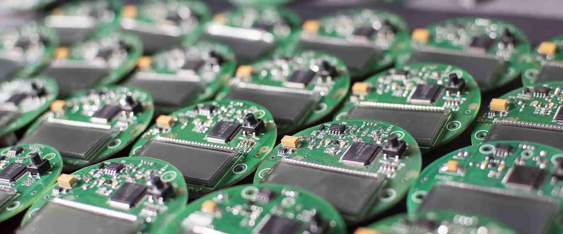
Xilinx XA7A50T-1CPG236I is designed to be a Field Programmable Gate Array (FPGA) with embeddable design. This aligns with the Surface Mount Technology (SMT) that permits the designer to place the electronic components directly on the surface of the circuit boards.

I/O Count

Input and Output, interpreted as I/O is used to determine the number of inputs and outputs in a Field Programmable Gate Array (FPGA). The inputs are typically taken or sourced from external or โ€œoutsideโ€ components and the circuit would process these inputs before releasing the outputs.

The general idea is to choose FPGAs that have several I/Os, because that increases the number of input and output options in the circuit.

A total of 106 Input and Output (I/O) pins are attached to the Xilinx XA7A50T-1CPG236I FPGA.

Operating Temperature

The Operating Temperature of an FPGA plays an important role in its regulation. This is because of the regulation of the temperature to prevent the circuit from going aboard when functioning.

The Xilinx XA7A50T-1CPG236I FPGA has an Operating Temperature of ~40หšC (minimum) and 100หšC (maximum).

Xilinx XA7A50T-1CPG236I Datasheet

The datasheet of the Xilinx XA7A50T-1CPG236I includes these specifications:

Technical InformationValue
Transceivers2
Number of Logic Elements52,160 LE
Operating Voltage Supply1 Volt (V)
Distributed Random Access Memory (RAM)600 kbit
Mounting Type/StyleSurface Mount Technology (SMT)/Surface Mount Device (SMD)
Data Rate1.25 GB/s
Number of Logic Array Blocks (LABs)4,075
Moisture Sensitivity Level (MSL)3
Embedded Block RAM2,700 kbit
Package CaseCSBGA-236

Why You Need the Xilinx XA7A50T-1CPG236I for Your Automotive Circuit Designs

Wondering why you need to invest in the Xilinx XA7A50T-1CPG236I FPGA for your next automotive circuit designs and applications?

We have uncovered some of the reasons why you should prioritize using this Integrated Circuit (IC). Here are a couple of the reasons:

1. The Circuit Board Operates at Higher Frequencies

Time is of the essence when designing circuit boards, especially when working with complex designs as FPGAs. Hence, anything that can help in reducing the time spent on prototyping and designing the board is very much appreciated.

That is one of the reasons why we are certain that the Xilinx XA7A50T-1CPG236I IC will be very desirable for designers looking to cut down on time spent working on the board.

The higher frequency operation of the board takes a cue from the 3 Gigahertz (GHz) maximum operation of FPGAs under the Artix-7 family. In addition, these boards offer excellent signal processing culled from the dual-embedded development platforms:

  • Development Board 2 (DB2)
  • Development Board 3 (DB3)

2. Excellent Clock Management

The clock architecture of the Xilinx XA7A50T-1CPG236I is excellent. Like the varieties of circuit boards under Artix-7, it offers jitter filtering, frequency synthesis and phase shifting.

In addition, the clock architecture of the Xilinx XA7A50T-1CPG236I includes:

3. Multiple Global Clock Lines

The global clock lines on the Xilinx XA7A50T-1CPG236I are 32. With the universal or global perceptive, it is easier to regulate and decide on which clock functions to leave and which to turn off.

For example, the designer can decide to turn off the clocks in specific regions as a way of reduction power consumption on the circuit board.

4. Synchronized Data Analysis

Analyzing or combining data in a Field Programmable Gate Array (FPGA) takes time. However, with the synchronized function provided by Xilinx XA7A50T-1CPG236Iโ€™s clocks, it can be made simpler.

For example, these clocks can aid in:

  • Providing higher rates of clocking, especially at an extra cycle of latency.
  • Reading, writing and accessing the memory of the Integrated Circuit (IC).
  • Clocking the address of any input into the Field Programmable Gate Array (FPGA).

5. Circuit Board Debugging

Debugging a circuit board helps the designer to find errors and fix the same on time. On the Xilinx XA7A50T-1CPG236I, this is done via the JTAG debuggers.

Artix-7 FPGAs (of which Xilinx XA7A50T-1CPG236I is one of it), come with Onboard Debug Module. This aids in simplifying the process of debugging the board, as well as integrating multiple inputs via its dedicated physical interfaces.

How to Buy the Xilinx XA7A50T-1CPG236I

Interested in the Xilinx XA7A50T-1CPG236I but unsure of the things to look for before adding it to your cart?

With these tips, you should be able to make the right decision:

1. Understand the Applicable Cases

It is true that the Xilinx XA7A50T-1CPG236I is designed for automotive applications. Yet, it wouldnโ€™t be a bad idea to find out the possible use cases. Which type or class or automotive can it be used for?

You can ask your designer or read through the datasheet to be certain.

2. Cost of Purchasing the Board

What is your budget for the Xilinx XA7A50T-1CPG236I? The cost is one important factor to consider. For emphasis, the rice range of the Xilinx XA7A50T-1CPG236I can differ by designers, as well as by the specifications.

You may, however, be able to get a discount if you are placing orders for more of the board. Find out the Minimum Order Quantity (MOQ) from the supplier to see if you can get a discount for huge volumes.

3. Preloaded Design

Granted, designing a Field Programmable Gate Array (FPGA) requires a strict attention to details. Giving the programmability and configuration options, it is essential not to make mistakes.

To that end, consider buying a Xilinx XA7A50T-1CPG236I FPGA with a preloaded design. This inspires you with ideas on how to design the board. You can choose to walk with the current design or take some ideas out of it to build something better.

Conclusion

We believe that this article explains in detail, the technical specifications of Xilinx XA7A50T-1CPG236I, including the reasons to choose it and how to buy one. Now, go ahead to shoot us a mail or use the contact us page to get a quote for the circuit board from RayPCB.

Technical Specifications of Xilinx XA7A35T-1CSG324I

Xilinx Spartan-6 FPGA

You have come to the right place if what you are looking for is an FPGA that cuts down on power consumption and improves performance. This solution is peculiar to Field Programmable Gate Arrays (FPGAs) in the Artix-7 series.

This family of Integrated Circuits (ICs) is manufactured by Xilinx and is designed to help the consumers get improved performance on their electronic devices.

Technical Specifications of Xilinx XA7A35T-1CSG324I

Here are some of the technical attributes of the Xilinx XA7A35T-1CSG324I FPGA:

Screening Level

Field Programmable Gate Arrays (FPGAs) are subject to screening. This is to check for the optimal performance of the circuits. The Xilinx XA7A35T-1CSG324I is not different. It is subjected to a series of screenings that are industrial-based.

That way, it becomes impossible for the engineers not to detect any defect on it. As it is designed for use in automotive applications, it makes sense that the industrial screening level is used. Automotive are high-powered and only an industrial screening of such magnitude can be used to determine the feasibility of the circuit in the test of time.

Temperature

The temperature of a Field Programmable Gate Array (FPGA) is an important element to consider. In the case of Xilinx XA7A35T-1CSG324I, its minimum operating temperature is ~40หšC. The maximum operating temperature is pegged at 10หšC (TJ).

However, the circuit has a maximum operating temperature of 210. The rule of thumb is to ensure that the circuitโ€™s temperature doesnโ€™t exceed the rated values, as that could have negative effects on its functionality.

Finishing

The finishing of an FPGA is also important. The Xilinx XA7A35T-1CSG324I has a lead finish, comprising Tin, Silver and Copper.

Propagation Delay

The role of propagation delay is to reduce the timeframe between the propagation or programming of an Integrated Circuit (IC) and its full functioning. The propagation delay on Xilinx XA7A35T-1CSG324I is 130ps.

The other technical specifics of the Xilinx XA7A35T-1CSG324I are:

Technical InformationValue
Standard Package IDLFBGA
Speed Grade1
Operating Supply Voltage1 Volt (V)
RAM Size225 KB
Part StatusActive
Mounting TypeSurface Mount Technology (SMT)
Peak Package Temperature100
Number of Logic Cells33280 LE
Number of Registers41600
Number of Pins324
Embedded Memory1.76 Mbit
Number of Inputs and Outputs (I/Os)210
Number of RAM Bits1843200
Number of CLBs/LABs2600

Innovative Designs of Xilinx XA7A35T-1CSG324I

As mentioned earlier, Xilinx XA7A35T-1CSG324I belongs to the Xilinx Artix-7 series. This is one of the series of FPGAs designed by Xilinx.

Here are some of the innovative designs that come with this FPGA series:

1. Integrated Development and Upgradable Design

One of the things designers or engineers of circuit boards look for is the programmability of the board. This isnโ€™t so easy to find, as some of these boards donโ€™t support that feature. For example, the Xilinx XA7A35T-1CSG324I doesnโ€™t have the in-programmability function, which might be a bit hard to program it fully.

That notwithstanding, the Artix-7 series where it belongs has innovative features, such as upgradable design and integrated development. For the upgradable design, we are talking about the faster configuration of the circuit. This empowers the designers to reprogram or modify the circuit to adapt into a wide range of applications.

Thus, it may be possible to use the Xilinx XA7A35T-1CSG324I FPGA in other high-powered applications, other than automotive.

For the circuit board integration, it is enabled by the dual integration of Xilinx XA7A35T-1CSG324I with two other boards. These are:

  • Zynq UltraScale + MPSoC Development Kit (DEVKIT)
  • Zynq UltraScale + MPSoC system

Through this interoperability, the Xilinx XA7A35T-1CSG324I FPGA would be used for developing and testing a variety of embedded circuit systems.

2. Extensive Onboard Resources

Circuit board designers appreciate working on a board that has a plethora of onboard resources. These are the resources used for fast-tracking the functions of the board.

The Xilinx XA7A35T-1CSG324I, like other Artix-7 FPGA series, has a variety of onboard resources. These resources include:

Development Board Reset

Letโ€™s assume that the designer made a mistake that he wishes to correct. With the development board reset feature, he would be able to do that.

On many Artix-7 boards, the reset feature comes in the form of three buttons. On a touch, these buttons can either:

Bitstreams Storage

There is a dedicated 32GB SDRAM Memory that handles the storage of Bitstreams on the Xilinx XA7A35T-1CSG324I. In addition, the storage provides for:

  • Easy transfer of Bitstreams either from the circuit board to another or from another circuit board to the FPGA.
  • Excellent programming of the Bitstreams into the development board.

Debugging Features

The Xilinx XA7A35T-1CSG324I also comes with debugging diagnostics that are provided through a Universal Serial Bus (USB) port.

3. Guaranteed Uptime

Keeping the development board active during the programming is very essential. This might not be possible if you were only depending on the batteries โ€“ which would be drained of power later.

However, you can count on the guaranteed uptime provided by the excellent Lithium-Ion batteries that can last for several weeks.

In addition, the development board has several power sources, giving the users multiple ways to recharge. Some of these power sources are wall sockets and solar panels.

4. Varieties of Physical Interfaces

With more tools to work with, designers will have little or on challenge with getting the job done. This is excellent because the Xilinx XA7A35T-1CSG324I FPGA has a variety of physical interfaces.

For example, it has the duo of SATA and MicroSD interfaces to bolster data storage. There is also the provision of Gigabit Ethernet that enables clear communications and operations.

Concluding Thoughts

Working with a Field Programmable Gate Array (FPGA) requires patience and a solid budget to fit into the project. Note that the Artix-7 series from where the Xilinx XA7A35T-1CSG324I comes from, has some challenges. These issues range from limited use of the development board to less-complex settings and more time spent on programming.

If you can overlook that, it may not be a bad idea to invest in the Xilinx XA7A35T-1CSG324I. With the help of our experienced team of designers at RayPCB, we will help you get the most out of the development board.

How Panasonic MEGTRON6 R-5775 Laminate Impacts High-speed Transmission of Data Communication

Shengyi S1600 pcb

Selecting the right PCB material is important for a PCB performance. In the past, FR4 material was typically specified. However, with high speed designs, it is important to use the right laminate. It is advisable to use a material that features a low dielectric constant. This helps to ensure the greatest signal performance. Also, it helps to reduce signal loss or phase jitter of the signal.

There are certain factors to consider when choosing a PCB material. The electromagnetic loss and environmental stability are important factors. Not all PCB laminates are ideal for some applications. The Panasonic MEGTRON6 R-5775 laminate is the topic of discussion in this article.

What is the Panasonic MEGTRON6 R-5775 Laminate?

Panasonic MEGTRON6 R-5775 laminate is a high speed and low loss material. This material features excellent thermal performance and HDI. Also, this material is specifically designed for high frequency PCB applications. Therefore, this explains the reason behind its low Dk and Df.

The electrical properties of Panasonic MEGTRON6 R-5775 laminate are competitive with PTFE-based laminates. However, this PCB laminate offers improved processability. Hence, this advanced feature offers designers great benefits in system performance for telecommunication applications.

Also, this material is suitable for low loss multilayer PCBs. This advanced multilayer PCB material allows greater-capacity data transmission. Therefore, this contributes to the 5G mobile communication systems. Panasonic MEGTRON6 R-5775 laminate features no halogen constituents. Also, this material doesnโ€™t contain bromine, fluorine, and chlorine. Therefore, it is safe for the environment.

The low dissipation factor and dielectric constant contribute to its low transmission loss. Also, this PCB laminate features great mechanical and thermal properties. These properties make this material perform well in extreme temperatures. Also, Panasonic MEGTRON6 R-5775 laminate is highly resistant to heat.

Properties of Panasonic MEGTRON6 R-5775 Laminate

It is very important to know the properties of this PCB material. These help you to understand its performance and functionality.

High decomposition temperature

The decomposition temperature (Td) value of this material is 410 degrees Celsius. Therefore, this material features a high decomposition temperature. This means that it can perform well under a high temperature without decomposing chemically. Also, this material will start decomposing chemically when exposed to a temperature above 410 degrees Celsius.

Low dielectric constant

The dielectric constant of this material is very low. Panasonic MEGTRON6 R-5775 laminate has a Dk value of 3.71 at 1 GHz. At 10 GHz, the Dk is 3.61. Also, this material features a stable Dk across a wide frequency and temperature range. This property contributes to this materialโ€™s low loss transmission.

High glass transition temperature

The glass transition temperature of MEGTRON6 R-5775 laminate is 185 degrees Celsius. Therefore, Panasonic MEGTRON6 R-5775 laminate is a high Tg material. Also, it offers great performance when used in varying temperature degrees.

Low dissipation factor

The dissipation factor of MEGTRON6 R-5775 laminate is very low and stable. Also, it has a Df value of 0.004 and 0.002 at 10 GHz and 1 GHz respectively. Also, this electrical property measures the degree of loss when electricity in an insulator discharges. Materials with low Df are more efficient as insulators. Therefore, this PCB material reduces electrical signal loss.

High peel strength

The peel strength of Panasonic MEGTRON6 R-5775 laminate is 0.8 KN/m at IPC-TM-650 2. 4. 8. Therefore, it maintains high peel strength.

Low coefficient of thermal expansion

The CTE before Tg at X and Y-axis is 14 and 16 ppmo/C respectively. The Z-axis CTE value before Tg is 45 ppmo/C. After Tg, the Z-axis CTE is 260 ppmo/C.

Basic Specifications of Panasonic MEGTRON6 R-5775 Laminate

Panasonic MEGTRON6 R-5775 laminate is a series that features some laminate and prepregs.

Panasonic MEGTRON6 R-5775 laminate series include:

  • R-5775(N)
  • R-5775(K)
  • R-5775(G)
  • R-5775(S)*
  • R-5775(R)*

Panasonic MEGTRON6 R-5775 Prepreg includes:

  • R-5670(N)
  • R-5670(K)
  • R-5670(G)

Benefits of Panasonic Halogen-free MEGTRON6 R-5375 Laminate

Offers low transmission loss

Signal loss is a great problem in high frequency PCBs. Therefore, it is important to use material that offers low transmission loss. This material tends to offer high data transmission. Also, Panasonic MEGTRON R-5775 laminate contributes to the development of the communication system.

Free of halogen constituents

This PCB laminate is free of halogen constituents.  Therefore, it is very safe for the environment. The demand for environment-friendly PCB materials for PCBs is growing. Also, the use of this material helps to maintain flame retardation in circuit boards.

Offers excellent heat-resistance

Panasonic MEGTRON R-5775 laminate greatly resists high heat. Therefore, this material enhances reliable operation. This multilayer PCB material features excellent reliability in extreme temperature environments. Also, the thermal properties contribute to this feature.

Improves ease of manufacturing of multilayer PCBs

Panasonic MEGTRON R-5775 Laminate enhances the processing of multilayer PCBs with more than 20 layers. In addition, this laminate offers excellent ease of manufacturing of multilayer boards.

Adheres to UL 94 V-0 flammability

One of the best advantages of this PCB material is its adherence to UL94 V-0 flammability. Therefore, this material features flame retardation.

Applications of Panasonic MEGTRON R-5775 Laminate

Panasonic MEGTRON R-5775 laminate is an advanced PCB material specially designed for high frequency PCB applications. Also, this PCB material is ideal for use in the following applications:

High-speed transfer and computing application

Panasonic MEGTRON R-5775 laminate is widely used in high speed transfer and computing applications. This is because of its signal integrity and low loss transmission features. Therefore, this material plays a crucial role in this application. Panasonic MEGTRON R-5775 laminate offers great benefits when used in this application.

Telecommunication system

The telecommunication system is heavily dependent on low loss PCB materials. High-speed signal transmission is very crucial in this application. Hence, this explains the high demand for Panasonic MEGTRON R-5775 laminate. Also, this laminate offers high speed data transmission. This helps to contribute to the telecommunication system.

Conclusion

PCB designers should specify laminates that provide optimal price-performance ratio. Therefore, it is important to research and analyze PCB materials. This article has evaluated and analyzed the properties and benefits of Panasonic MEGTRON R-5775 laminate.

LGA PGA BGA: What’s the Difference Between the Grid Arrays?

LGA PGA BGA

Over the years, IC (integrated circuits) have significantly evolved. Earlier on, in the 90s, ICs were super huge. However, in the 21st century, we have ICs that are downright tiny. Manufacturers utilize these tiny microscopic ICs to develop small but powerful CPUs that manage powerful computers. However, when going over this topic on CPUs, you will likely come across words such as LGA, PGA, and BGA. These terms, which we shall discuss later on, describe various types of IC packages. However, these packages bear differences that breed variation. But are these differences that we are talking about? And out of the three, which is the best IC to utilize?

Ball Grid Array

Ball Grid Array (BGA) packages utilize tiny solder balls to form connections. These balls follow a square grid arrangement consisting of rows and columns on the backside of an IC. Due to this design, these packages can form high-density connections. The connections are so many such that they can even double the number of connections made on PGA packages.

BGA solder balls offer short connections, which leads to a chipset with impeccable performance.

Advantages of utilizing BGA packages

BGA packages have the following benefits:

  1. Optimal space utilization โ€“ BGA packages are tiny. They hence take up less space. However, their small size does not lower their performance. Therefore, you can generate tiny gadgets that are super powerful using this incredible Package.
  2. Heat dissipation โ€“ BGA packages dissipate heat impeccably. Therefore, they rarely overheat.
  3. Low impedance โ€“ BGA packages have low impedance because of the short lead connection paths. The packages are hence able to propagate signals pretty fast.
  4. Easy to unsolder โ€“ BGA packages are super easy to unsolder. The unsoldering process is also efficient such that it does not damage the BGA package or the PCB.
  5. Deballing is made possible โ€“ BGA packages let you remove old, worn-out solder balls via a process known as deballing. In doing so, you optimize your BGA to produce excellent outputs.
  6. Reballing โ€“ BGA packages let you populate your Package with new solder balls through a process known as reballing.
  7. Portability โ€“ BGA chips are portable. That means that you can eject them from one device and mount them onto another device, and they will still function well.
  8. Impeccable thermal and mechanical properties โ€“ BGAs have impeccable thermal and mechanical properties. Due to these properties, you can utilize this gadget as a CPU for your computer.

Disadvantages of utilizing BGAs

pin grid array

Even though BGAs have a lot of advantages, they still have some disadvantages. These disadvantages include:

  1. Solder inspection โ€“ To inspect BGA solder joints, you must utilize x-rays. That is because these packages use their bottom side to make connections making it hard to access the component-to-PCB link.
  2. Hard to repair โ€“ the access limitation factor greatly hinders the repair process. To carry out BGA repair, you must utilize special equipment and skills.
  3. Challenging to solder โ€“ To solder BGA packages onto PCBs, you have to utilize special equipment.
  4. Application limitation โ€“ BGA packages only work on multi-layer circuit boards. They, therefore, have limited applications.

Pin Grid Array (PGA)

Pin Grid Array (PGA) are IC packages that manufacturers mostly utilize to make processors solely. While BGAs utilize solder balls to create connections, PGAs utilize tiny pins to do the same.

PGAs also arrange their pins in a square grid that features rows and columns. However, the array arrangement and the amount of connection made vary. Therefore, PGA has a lot of variants and hence varying CPU sockets.

PGA pen rows are arranged offset or in parallel. These pen rows are labeled, and you can pinpoint them using unique letters and numbers.

PGA Types

  1. Ceramic Pin Grid Array (CPGA) โ€“ CPGAs feature a semiconductor chip fixed onto a ceramic carrier that conducts heat. Intel Pentium first-generation CPUs were made out of these packages.
  2. Plastic Pin Grid Array (PPGA) โ€“ In PPGA, the semiconductors chip carrier is a plastic component. These package variations are cheap, and they have impeccable thermal properties when you compare them with other PGAs. They also have better electrical performance when you compare them with ceramics.

PPGA application areas over the years include:

  • Application in the Celeron processor
  • Application in the Pentium MMX CPU
  • Staggered Pin Grid Array (SPGA)ย โ€“ SPGAs feature connection rows that are “staggered.” These PGA variations are significant for CPUs that bear more than two hundred connections. That is because the layout of the offset provides more space.

SPGA application areas include:

  • In the Pentium process
  • Modern CPUs
  • Flip Chip Pin Grid Arrays (FCPGA) โ€“ In this package variation, the IC attaches onto the carrier’s top.

The application areas of this Package over the years include:

  • Application in the Pentium III
  • Application in some Celeron CPUs

Since PGAs feature pins, circuit boards that utilize these packages feature holes. The pins go through their corresponding holes, creating a connection. Since the holes are pre-made, this process does not need much pressure.

Land Grid Array (LGA)

Land Grid Array packages and PGAs are two opposite sides of the same coin. What this means is that these two components do the same job, but they have different connection designs.

In LGAs, contact pins protrude from the mainboardโ€™s base. The CPU, on the other hand, features contact points that match those of the circuit board. To create a connection, merge the pins to their corresponding points, and you are all set.

Application areas of this Package over the years include:

  1. In Celeron CPUs
  2. In Pentium CPUs
  3. And lastly, in Xeon CPUs

Advantages of utilizing LGAs

Advantages of utilizing LGAs include:

  1. The chip size โ€“ LGAs are tiny. Hence, they are space-efficient, and you can utilize them to create small, powerful gadgets.
  2. Pin size โ€“ LGA pins are super small. That means that you can easily fit many pins on a small area.
  3. Not prone to damage โ€“ LGA pins are on the circuit board. On the other hand, the sockets bear points that are not prone to damage.

PGAs VS LGAs

PGA contact pins protrude from the socket; this makes the circuit board less prone to damage. On the other hand, in LGA, contact pins protrude from the circuit board, making it more prone to damage.

Another difference is that repairing pins in PGA packages is easier than repairing pins in LGA packages.

Conclusion

LPA PGA and BGA are incredible IC packages that have been in the tech market for years. Of course, these packages bear advantages and disadvantages. However, overall their performances have led to the tech evolution. Now you can utilize small and powerful devices such as phones to carry out complex computations.

Cracking The Electronic Assembly Kits Code

through-hole assembly process

Do you need spare parts for a device that you work on? Are you someone who likes to work with your hands? Want to learn how electronics work? Want an exciting hobby that will get you out of the house and off the couch? If so, then do some research on electronic assembly kits.

Do you know the different existing types of electronic assembly kits? We will look at what we mean by this electronic assembly and the two different assembly kits. Additionally, we will dig into each of these types and look at some examples of these assembly kits. Finally, we will look at the importance of each of these types of assembly kits.  

What is electronic assembly?

Electronic assembly kits are a relatively new trend in the world of technology and DIY-enthusiasts. They are designed to be educational as well as challenging. We define electronic assembly as the process involving bringing together, soldering, or mounting the electronic circuits and components in a printed circuit board (PCB) board to do single or multiple specific functions. The process is important in manufacturing electronic components like toys, remotes, television sets, engines, phones, computers, etc.

What are electronic assembly kits?

Electronic assembly kits are already assembled kits that include assembling all the pieces of certain electronic appliances. The main aim of these kits is to help the users learn the process and the science of electronic systems through active practice. These electronic assembled kits are universal since diverse people use them to do their daily activities. There are two different types of electronic assembly kits;

  1. Kits for kids
  2. Kits for adults

What are Electronic assembly kits for kids?

Manufacturers design these electronic assembly kits to make them easier for the kids to use. Kids at the age of 8-12 years use these kits to learn electronics, start a mini fan motor, or light a bulb. Young children and early learners engage in these projects for fun. However, adults do not find these activities engaging or exciting. Therefore, electronic kits for adults have more complex features and an instruction manual to help them assemble the components. The kids should find kits that fit their skills and adapt to active learning progressively.

Types of electronic assembly kits for kids

There are several examples of electronic assembly kits for kids, these involve;

  1. LittleBits, an easy-to-use block of electronics that fit together with magnets. They use them to make learning fun and learn about circuitry. Kids can build a night light, guitar, electronic pets, and many other gadgets. Kids can use these kits at home, school, and anywhere they like.
  2. LightUp โ€“ kids fit these kits together with magnets to make circuits. For instance, some of the light kits, the light Tesla kit, helps us teach kids programming to build cooler projects; we also use them to teach the kids about technology, science, and technology.
  3. MakeyMakey kits are easy to construct with gadgets such as video games controller, and the kit does not need any programming skills for kids to start inventing. They also install important skills in science to kids who use them for fun and learning.

What is the importance of electronic assembly kits for kids?

An average person has no clue how the electronic assembly kits function except plugging them in replacing the battery to power them. There are many reasons for giving kids these kits to assemble. However, kids think it is only giving them a playing toy or having fun. The following are examples of electronic assembly kits for kids;

  • Electrical assembly kits teach them important skills. In addition, using these kits is an interesting way of introducing kids and developing interests in science, technology, engineering, and mathematics.
  • Teaches them to respect their electronics. Kids having the kits learns to take care of and respect their gadgets since they understand how to assemble the components. Furthermore, they will understand how difficult it is to repair a component in case of a malfunction.
  •  Electronic assembly kits help save them money. Kids should learn how to fix different electronic circuits using their electronic kits. Additionally, kids spend much time learning technology and science through these electronics assembled kits.
  • You will find out that these electronic assembly kits are very useful. Light-up hats, toys, or radios, are examples of electronic assembled kits. They are practical components that bring personal satisfaction to the kids, as they can easily assemble them.
  • Working with the electronic assembly kits can be a family activity. Kids use these electronic assembly kits in building devices at home. Therefore, they are thrilled when they use gadgets that they build rather than the ones bought from the stores.

What are electronic assembly kits for adults?

Adult electronic kits are complex pre-assembled kits comprising the components and the printed circuit board. The adults use different complex features to learn using these kits for fun by engaging them. It is becoming common to find new electronic kits designs for adults or individuals searching for an interesting kit.

What is the importance of electronic assembly kits for adults?

Electronic assembly kits for adults have much-known importance. The following are the advantages of electronic assembly kits for adults;

  • Adults use electronic kits in the learning process. For instance, OSEPP robotic functional kit help adults learn a programming language by practical application on OSEPP robot.
  • It helps adults develop useful skills. The kits may make the adults learn and apply thinking skills in making these gadgets. The skills developed include; learning skills, teamwork skills, communication skills, and more.
  • The kits reduce the construction cost since they are easy and they contain an instruction manual for building these gadgets.

Types of electronic assembly kits for kids

  1. OSEPP-Wheeler Balancing Robot kit. This kit helps adults easily build a 2-wheeler balancing robot kit that can move through all terrains. They prefer these kits in building projects since they are easy to build and control. The kits also have a control setup manual on how to construct them.
  2. Important electronic parts kit. Electronic experts mainly use it to do their work. The kit comprises electronic components such as capacitors, rectifiers, diodes, resistors, and 275 other electrical components.
  3. ย Arduino basics starter kit with UNO-03. This kit can build a voltmeter, buzzer circuits play a melody, and LED game. It also comprises about 100 pieces and an instruction manual; hence, it does not require any skill to begin using.
  4. OSEPP robotics functional kit-MECHF-01. The OSEPP Function kit is an amazing kit that can build hi-tech projects. There are different components in this type of kits, like functions and high-level sensors. We can customize the sensors and Bluetooth technology to perform the task of adjusting light and also control robots from their smartphone app.

Conclusion

This article has looked at the electrical assembly kits, their categories, and advantages. Adults and children use different electrical assembly kits in their daily activities.

Thus when you buy electronic assembly kits, you get a variety of necessary components to complete a specific project. Many times, you will only need to supply your own PC and screwdrivers! You are provided with the correct tools and step-by-step instructions that make it easy for even the most novice of hobbyists to build one from scratch. This gives you the ability to fully understand how each component functions and how each piece interacts with the other.

Best Paying Electronic Assembly Jobs near Me

pcb assembly jobs

Electronic assemblers are crucial to the tech industry and the world at large. They connect electronic systems and parts according to user specifications. Such electronic assemblers also analyze blueprints and schematics following their client’s specifications. Therefore, if you have a working electronic device, that might be so thanks to an electronic assembler. However, electronic assemblers do more than their names dictate. This article will focus on the major concern you have – ‘electronic assembly jobs near me.’ We know that finding a job even with a lot of electronic assembly experience can be challenging. So, we are here to make it easier. Are you ready to score a job in the electronic assembly market?

Electronic assemblers work with various equipment and hand tools to execute their duties. Due to this, they need great knowledge of the mechanical industry. An Electronic assembler can:

  • Inspect equipment efficiency
  • Perform repairs
  • Replace defects

Also, electronic assemblers have to adhere to safety precautions while at work to prevent any accidents. They also work with the maintenance team to assemble electronics to completions.

In the process of undertaking one job, electronic assemblers gain a lot of knowledge that they can apply in various industries. Therefore, they simply have a wider job scope. However, before we put a pin to that fact, let us first explore the responsibilities of an assembler.

The Responsibilities of an Assembler

Here are some responsibilities that electronic assemblers undertake:

  • First, they produce electronic devices by assembling and then soldering components on electronic circuit boards.
  • They build, test, and repair interlock devices
  • Helping engineers troubleshoot systems
  • They perform tests of high quality and pass the IPC standers
  • Making use of manual dexterity skills, visual acuity, and oral communication skills.
  • They test, check, serialize, and pack electronic boards under ESD controls and procedures.
  • Electronic assemblers install various components using the thru-hole procedure.
  • They work with wiring diagrams and blueprints.
  • Electronic assemblers are certified for wire wrapping, ESD, and soldering.
  • Electronic assembler read:
  • Drawings,
  • Schematics, and
  • Instructions

To properly wire and assemble client products according to customer and ISO standards.

  • They perform routine maintenance on machinery, which lowers accidents rates.
  • They receive progressive promotions as they continue to gain experience in the field.

As you can see, electronic assemblers have a lot of responsibilities which now leads us to the next question. How much do you think an electronic assembler earns annually? With such a long list of responsibilities, I hope your guess is right!

Electronic Assembly Salaries

Electronic Assemblers earn an average annual salary of about 31,454 USD which we can break down to 15.12 USD per hour. However, note that this is the average salary as the actual salaries vary due to:

  • Experience differences
  • Skillset differences
  • Working positions

Due to these differences, the actual annual salary of electronic assemblers ranges between 26,000 USD and 37,000 USD (for the top earner). The top earners can earn up to 11,000 USD more than the 25th percentile. However, to become a top earner, should be resilient in your job.

Electronic Assembler Personal Traits and Skills to help score Electronic Assembly Jobs Near me

This section shall break down the various personalities and skill sets you require to score when you are searching for ‘electrical assembly jobs near me.’ To take things up a notch, we shall also add in the percentage of people in the electrical assembly industry who use these skills. The references are courtesy of various resumes of people working in the industry to date.

Hand tools (6%)

Involves inspecting and assembling PC connectors while following client specifications. It also includes operating assembly machines and using actual hand tools to carry out tasks.

Dexterity (6%)

You should have perfect attendance

Assembly instructions (19%)

Have the ability to read various work orders keenly to determine assembly instructions and material requirements.

Sub-assemblies (6%)

Lighter electronic assembling involves simpler wiring diagrams and appropriate documentation.

Electrical assembly (5%)

Involves inserting electronic components onto circuit boards using various methods such as:

  • Soldering techniques
  • Hand insertion

Suppose you are looking to write a resume to score electrical assembly jobs near you. You will want to add some or all of this skill set into your resume. They spice it up and show and that you have the skill sets required to take on an electrical assembly job.

List of Electronic Assembly Jobs near Me

And now, for the main event, let us look at some electronic assembly jobs that you can easily find in your neighborhood. The jobs are well paying, and they utilize your skill sets to the fullest.

Electrical Assembler

Well, all through we have gone through what an electrical assembler does, their annual salary and skillsets. So all those factors hold for this case.

Solder technician

If you have Electrical Assembler skills and experience, then you can take on a soldering technician job. The two jobs have some differences, of course. For example, the annual salary of a solder technician is 645 USD higher than that of an electrical assembler.

However, even with this salary difference, these two jobs have one common ground. When you compare the skill sets required to take on these two jobs, you will note that some of them collide. For example, in both, the employer requires the employee to possess:

  • Hand tool skills
  • Dexterity skills
  • Ability to follow assembly instructions

Assembly Technician

Assembly technicians assemble small components to generate new products according to user specifications. As an assembly technician, you will get to:

  • Perform diagnostics
  • Provide manual instruction guidelines
  • Analyze different designs to generate optimal output

Assembly associate

An assembly associate assembles parts and components according to set instructions and diagrams.

As an assembly associate, you should expect to:

  1. Operate machinery
  2. Maintain records
  3. Adhere to production goals and schedules

Assembly associates earn 2,726 USD less than Electronic Assemblers.

Assembler and Quality Control

Assembler and quality control have some skill sets that collide with Electronic assembly. For example, an employer in both scenarios will be looking for these skills in your resume:

Hence, you should highlight these three skills to give you an upper hand in gaining this job.

On average, Electronic Assembly jobs pay 984 USD more than Assembler and Quality control jobs annually.

Conclusion

Sometimes it gets tricky when searching for “Electronic Assembly Jobs near me.” In most cases, we attribute this to:

  • A badly written resume,
  • Not knowing which jobs fit your skillset, and
  • Thinking that you are only restricted to the job you studied for.

However, if you apply the tips provided in this article, you will, without a doubt, score a job sooner than you expect.

Elecrow PCB Review: Cheap, Quality PCBs for Your Next Project

Nelco N4000-13 High-Speed pcb

If you’re looking to make your PCBs, you’ll love this company’s open-source hardware boards. You can make open-source hardware boards for the Arduino and IoT platforms or use their PCB assembly services to customize stencils. They even assemble everything sold at the Tindie store. Read on to find out more. But first, let’s discuss the PCB assembly process. There are a few things you need to know.

HASL finish

HASL is a standard surface finish used on many PCBs. It has long been a popular choice for its affordability and robustness. But its shortcomings have come to light, particularly with the advent of more complex surface mount technologies. Its disadvantages include leaving uneven surfaces, making it unsuitable for using fine pitch components. In addition, while it’s lead-free, other methods may be better suited for high-reliability products.

The HASL finish on Elecrow PCBS is a good choice for applications involving real current. Copper weight across all boards was within tolerance. In addition, all but one board had trace-net end solder mask witness marks that could be hazardous in real-current applications. The solder mask had scratched completely on one board, exposing a trace beneath, tested conducive to the pad at the trace net end. On another board, a via had significant scratches. Nevertheless, overall board quality is excellent.

HASL and ENIG finishes are similar, but HASL is less expensive. In addition, the ENIG finish has a flat surface that’s more conducive to soldering. ENIG is also preferred for high-pin-count and fine pitch components, as its flatness makes the placement of components more precise and enables controlled solder application. The latter finish also reduces the risk of shorts and opens.

HASL finish on Elecrow PCBA is a lead-free surface finish. HASL finish is an environmentally-friendly option, and its customers can select the color of the PCB. In addition to HASL finish, Elecrow PCB also offers fast shipping. The price of the HASL finish depends on the complexity of the design. However, the HASL finish makes a PCB more environmentally friendly than standard finishes.

Another option is immersion silver. This finish is more environmentally friendly and a good option for flat pack and fine pitch applications.

Green solder mask

The first thing that caught our attention about the Elecrow PCBs was the solder mask. As expected, it was green, but with some unusual features. The outlines of the XLR pins, for example, were not solid but rather had cuts in them. I noticed this problem even on the 4-layer board. Another strange feature we noticed is the solder mask color, which is inconsistent with other boards. In two cases, the solder mask color is red, while on the other, it’s orange. We speculated that these issues might be related to the PCBA process.

Another detail that we noticed was the size of the vias. While Elecrow’s website has a helpful illustration of the order process, this service does not include testing. This is because high-performance analog circuits are not easy to test. In addition, Elecrow’s PCBs are much smaller than a standard-sized PCB, and they have a minimum drill hole size of 0.3mm.

99% of all circuit boards have a green solder mask. However, you might opt for another color if you have special requirements depending on your needs. Solder masks can be printed or sprayed on the PCBs and are UV-exposed. Generally, green solder masks are more durable than others and lend themselves to visual inspection.

White and black PCBs are increasingly popular, although they’re not a perfect match for your product. For example, white PCBs tend to hide traces and are difficult to inspect without a bright overhead light. Moreover, a white solder mask does not look good with black silkscreens. However, if you’re looking for a professional-looking circuit board, you might consider using a white solder mask from Rayming PCB & Assembly.

Small vias

The Elecrow website shows how to order a custom PCB, but there is a catch. It does not provide testing services. Testing high-performance analog circuits is complex and requires a capable test kit. However, if you are a DIY designer or do-it-yourselfer who cannot buy or produce a prototype, then the Elecrow website will be your best bet.

When designing a PCB, it is essential to consider the layout. To choose the best layout for your PCB, you need to know the dimensions of the holes. The dimensions of the vias should be smaller than the thickness of the board. The corresponding hole size must also be bigger than the diameter of the hole itself. Choosing via size depends on the board’s size and purpose. The larger the PCB, the better, as older computing devices only accept bigger PCBs with through-hole components.

It is also crucial to choose a factory capable of manufacturing your PCB. The best factories can handle even the simplest PCB design, so choose a manufacturer with the requisite expertise and capability to manufacture your PCB. You should also know what to expect from Elecrow PCBs. You can order a prototype or a fully-completed board, depending on the complexity of your design.

The Gerber RS-274X file format is standard across manufacturers, making it easier to create high-quality prototypes. In addition, the rules of PCB design have become much tighter, with many manufacturers supporting 6/6 mil design rules, small vias, and a variety of PCB thicknesses. You can also use a low-cost $10 per ten-board-order price for the prototype. Finally, if you’re a beginner and want to experiment with PCB design, you can try TinySine.

Laser-cut stencils

The design and surface finish of laser-cut stencils are essential for a smooth solder paste transfer. The amount of paste deposited depends on the aperture size and design. An appropriate stencil will minimize the amount of solder paste deposited on the board, thereby maximizing solder joint strength and electrical functionality. Stencil printability is also dependent on the size of the aperture and the thickness of the foil.

A frameless laser-cut stencil is the most robust type of laser-cut stencil. It is suitable for high-volume screen-printing during a production run. It is permanently mounted within the stencil frame and features a mesh border to stretch the foil taut. This stencil type is ideal for components with an aperture wall smaller than 16 Mil, such as Micro BGAs. It also provides the highest level of positional accuracy and is suitable for use in temperature-controlled environments.

Laser-cut stencils for Elecrow are available in two sizes: one for the internal area of the board and another for the overall area. Laser-cut stencils should match the dimensions of a PCB’s ready-to-assemble state but should not be too small or too large for the board itself. Make sure that the PCB stencil’s internal area and the outer area are compatible with the parameters of your printer.

A laser-cut stencil is an excellent choice when solder paste is ideal for PCB panelizing. Its well-defined edges will make the placement of components easy and increase reflow rates. There are no other stencils that provide the same level of precision and accuracy. The design and thickness of the stencil are crucial in achieving the best results. The stencil is a product of polycarbonate and metal.

Conclusion

You should take the time to research and decide on the bare minimum requirements of a PCB manufacturer. A good PCB manufacturer will have expertise and experience and have the skills and equipment to manufacture your PCBs. A quality manufacturer will also provide testing services, a must for all high-performance devices. Elecrow’s website is an excellent resource for beginners looking to test their designs before making them commercially available.

Why You Should Prefer Underfilling BGA

Underfilling BGA

In the packaging of flip chips, the C4 between substrates and IC chips is pretty vulnerable to mechanical stress. That is due to the extensive CTE (coefficient of Thermal Expansion) mismatch that lies between the substrates and the silicon chips. Thus in case of a high thermal load, this CTE mismatch brings about significant stress to the C4 leading to reliability concerns. Manufacturers hence use a single underfill layer to efficiently fill this gap that exits between substrates and ICs. In doing so, they encapsulate various solder joints, which helps minimize reliability concerns. Over the years, this practice has been of much help to manufacturers. It is actually one of the most basic packaging procedures in the packaging of electronic gadgets. But what does this process entail entirely?

What exactly is an underfill?

An underfill is a thermoset epoxy that manufacturers apply onto flip chips to effectively reduce thermal stress. The thermal stress occurs due to the CTE mismatch between organic substrates and integrated circuit, of course.

Todayโ€™s underfills come in many different variations. Manufacturers utilize this variation widely to boost the board level (BL) reliability of various Ball Grid Array (BGA) components. They also utilize them to boost the performance of their PCBs.

BGA underfill substances achieve this feats due to their low mechanical and thermal load. These two features help them function well in harsh conditions providing optimal outputs each time.

However, before utilizing an underfill, manufacturers have to consider:

  • The underfillโ€™s intended use
  • The underfillโ€™s properties

In doing so, they get to assess how much BL reliability the underfill will offer. A miscalculation in this stage could cause catastrophic results.

Underfilling BGA Process, what does it entail?

BGA, as seen earlier, stands for Ball Grid Array. It is a special surface-mount packaging type that manufacturers use for:

  • The assembly of circuit boards
  • To permanently mount various microprocessor
  • To permanently mount other devices onto a circuit board

Ball Grid Array underfilling also lets you add interconnection pins. That is because, when working with a BGA component, you can utilize its entire bottom part instead of just using its perimeter. It hence provides a net result of interconnection pins that exceed those of flat and dual-inline packages. Interconnection pins are pretty fragile and also susceptible to a lot of damage from impact and moisture. Therefore, manufacturers also utilize underfilling BGA to shield the assembly of their circuit board by boosting:

  • Their thermal properties and,
  • Their Mechanical properties

How the process occurs

The BGA process helps create stable component attachments onto a PCB. It also helps create a circuit board that has impeccable thermal and moisture performance. However, this process is not easy to undertaking. Many people have to utilize special gadgets to achieve this feat.

Mostly, manufacturers use epoxies as their coating substance. However, other substances such as silicone and acrylic are also not so uncommon. With this substances in check, manufacturers then move on to underfilling BGA stage.

The underfilling BGA process is as follows:

  • Manufacturers apply the underfilling onto a particular corner or in a specific line along the BGAโ€™s or Micro CSPโ€™s edge
  • After applying the BGA, they then heat the micro CSP or the BGA using temperatures within the range of 125 โ€“ 1650C
  • They then utilize capillary action to effectively absorb the applied underfill substance under the Micro CSP and BGA
  • To cure the underfill, manufacturers maintain a steady temperature for about one hour or so. The time range shifts depending on the underfill component in use.

When the underfilling BGA process is over, you get a PCB that is super-efficient and durable.

How does the underfilling BGA process shield the PCB assembly process?

The underfilling BGA process provides an impeccable mechanical bond between PCBs and BGAs. It does so by shielding various solder joints from any physical stress.

The underfill substance also aids in efficient heat transfer between the PCB and various BGA components.

BGA reworking solution

Most underfill substances that manufacturers use in the underfilling BGA process are re-workable. What this means is that, in case of a defect, you, or the manufacturer, can replace or repair the parts. In addition, the repairing and replacing processes are easy to undertake, making it better than getting another device.

The ultimate goal of underfilling BGA is to reduce operating stress while at the same time reducing:

  • Processing time and,
  • Manufacturing cost

Special underfilling BGA process

A unique underfilling BGA process exists, which utilizes made-to-order components. These components are frozen to minimize the chances of contamination.

However, to utilize this component, you have to have a specific requirement in mind. That is because manufacturers apply this BGA underfills to precision and according to your needs.

Identifying various underfill BGA defects

To identify underfill defects in BGA, you need to utilize extreme magnification and cross-section testing. These two methods are almost always accurate.

Factors to consider in your test include:

  • Low-quality profile development
  • Heat damage
  • Improper print circuit board assembly preparing
  • Operator error
  • Inappropriate equipment

Common defects that you are likely to encounter include:

  • Open circuitry
  • Excessive voids found in the solder balls
  • Eccentricity of the solder balls
  • Coplanarity between PCB and BGA assembly

These are common defects that you are likely to encounter after carrying out your testing. However, after finding these defects, do not panic, as you can easily carry out BGA reballing or reworking.

Underfilling BGA applications

You can apply underfilling BGA in the following areas:

  • Inland grid array (LGA) devices โ€“ BGA application in LGA helps account for chip-scale consideration. It also helps account for the packaging density.
  • In Chip Scale Packages (CSP) โ€“ BGA application in CSP helps prevent any damages that may occur due to:
  • Vibrations
  • Shock
  • Weight
  • In chip-on-chip gadgets โ€“ you can apply the underfilling BGA on various chip gadgets.

Utilizing underfilling BGA helps reduce mechanical and thermal stress. It also helps boost the reliability of a Print Circuit Board via the underfilling process.

BGA packaging shields PCBs against cracking while at the same time reducing solder-joint stress. The net result of all this is a PCB that functions impeccably.

Conclusion

The modern market has a wide range of PCB variations to offer. Therefore, most people are now looking for reliability and efficiency, not just variation. The underfilling BGA process offers these two qualities at a low price. Using this simple yet efficient process, you can produce a PCB that can withstand great thermal and mechanical stress. Your PCBs will hence become unique in the modern market, and this is all it takes to take your PCB game to the next level.

Plat BGA Process for Microchip Design – Standardization for Printed Circuit Boards

Plat BGA

BGA (Ball Grid Array) is a pretty popular surface chip mount package that utilizes a grid of solder balls to create connections. However, this solder ball gets old and worn out. When this happens, you need to remove these old, worn-out solder balls and replace them with new ones. To achieve this, you have to utilize a process known as reballing, and that is where the plat BGA comes in. So what does the Plat BGA do? Why is it essential in Ball Grid Arrays? And why should you get it pronto?

A bit about Reballing

Engineers built BGAs to make an accurate chip to circuit board contact. Therefore, once a connection has been made, gaining access to the link becomes pretty tricky. But, sometimes circumstance, such as a worn-out solder ball, forces us to recreate every single solder ball joint for our chip to function well. If such as case has ever struck you, then Reballng might have been your only chance for redemption. Reballing entails the removal and replacement of old BGA solder balls.

Reballing is mostly undertaken on:

  • Computers motherboards
  • Gaming motherboards
  • Laptop motherboards

The reason behind the high number of reballing cases in these motherboards is a chip known as a Video Graphics chip. The Video Graphics chip gets hit by so many broken solder joints that require repair.

BGA chips also get hit by broken solder joints. However, BGA-chip-broken-solder-joint cases are not as many as those of Video Graphics chips, but they still cause alarm.

Effects of an incompetent Solder Joint

Bad BGA solder joints have adverse effects on a gadget. If, for instance, a bad solder joint hits your IC, it might render the IC useless. That might lead to your device not even turning on.

If your Video Graphics Card gets a broken solder joint, this might cause your screen to go blank. Unfortunately, that means that nothing will display on the screen until you fix the broken joint. That is why reballing is crucial.

Why do BGA chips require reballing?

BGA chips require reballing due to four main reasons:

  1. Simply due to overuse โ€“ After utilizing your BGA chip for a while, the solder joints grow old and get worn out. It becomes useful if you undertook reballing, or the chip would become utterly useless. The same case applies to Video Graphics Cards.
  2. Replacement purposes โ€“ sometimes BGA solder balls just need replacements with new ones.
  3. Upgrading purposes โ€“ Sometimes, BGA solder balls require an upgrade to match the modern market’s requirements.
  4. Overheating โ€“ When solder balls overheat, they affect their solder joints, leading to a joint break. But that is not the worst that could happen due to overheating. If the heat exceeds, it could cause harm to the Circuit Board leading to more damage. Therefore, you need to replace overheating solder balls pronto!

Where does Plat BGA come in?

Plat BGA is a Strong sheet of metal with many holes to accommodate multiple solder balls in the reballing process.

In most cases, you can make Plat BGA out of high-quality, durable steel. Therefore, you can heat the sheet directly using a BGA machine or a hot air gun to loosen the solder ball by melting the solder. When the solder balls are loose, reballing becomes super easy to undertake.

However, you need five more supplies to execute the reballing procedure efficiently.

The 5 supplies

These supplies are:

  1. Soldering Iron โ€“ It is a hand tool that helps you in the soldering process. Using this tool, you can easily heat up and melt soldering metal to fix broken joints between the BGA ball grid.

Soldering irons have two components in total, the heated metal tip, and the insulated handle.

  1. Soldering Paste โ€“ Soldering pastes is a popular component manufacturers use in the PCB assembly process. The primary purpose of this paste is to mount various components onto the surface of the PCB. Therefore, this component will come in handy when we are mounting our chip back onto the PCB.
  2. Desoldering wire โ€“ย A desoldering wire or simply a desoldering wick is an impeccably braided 18 โ€“ 42 copper wire. These copper wires have a rosin flux coating to boost their efficiency and durability. They usually come in roll variations.

The desoldering wire’s main job is to eject the solder that lies around and onto the broken solder joint. It does so by effectively soaking the joints solder using metal solder.

  1. BGA Chip Case โ€“ A standard case that you can utilize to hold your chip in place during the reballing process.
  2. Solder Balls โ€“ BGA solder balls are tiny solder components that take the shape of a sphere. You can find these components on the bottom part of the BGA chip. The main job of these balls is to make a competent chip to Circuit Board connections. Then, the chip utilizes these connections to send and receive electronic signals.
  3. BGA Reworking machine โ€“ It provides sufficient heat to help you remove or attach your BGA chip.

Advantages of utilizing Plat BGA in the Reballing procedure

If you are looking to employ Plat BGA to carry out Reballing, then here are some benefits that you are likely to reap:

  1. Saving on cost โ€“ Plat BGAs are not expensive. Hence, you can get one at a pretty low price and utilize it to get your BGA chip up and running.
  2. Easy to utilize โ€“ When working with the plat BGA, you’ll note that it is user-friendly. The grids that contain holes to fit the solder ball are super easy to spot. Then, to work with the grid, all you have to do is place the chip onto the grid, and you are all set.
  3. It can withstand high temperatures โ€“ Plat BGAs have a high melting point. Therefore, the chances of this metal sheet melting during reballing are pretty slim.

On top of all that, you also get to optimize your chip’s performance and efficiency.

Conclusion

Plat BGAs are, without a doubt, impeccable at what they do. These fantastic tools help revive broken solder joints in video graphic chips, IC, and other BGAs. In addition, they are easy to utilize, efficient, and cost-friendly, which makes them the perfect tool to use for reballing purposes. Therefore, if you have been struck by a broken solder joint, do not hesitate to work with this item. It does not disappoint.

The Low Cost Industry Leading FT1 BGA Assembly

FT1 BGA Assembly

The Ft1 BGA or simply the BGA 413 is an impeccable CPU socket that hit the market back in 2011. The CPU socket, just as the name implies, utilizes a Ball Grid Array (BGA) to function. Due to its efficiency, the Ft1 BGA has a lot of applications in the tech world. However, are these the only features that make up the Ft1 BGA? Does it bear more features and properties that make it stand out? And if so, is it worth working with?

About Ft1 BGA

Ft1 BGA is a CPU package built for AMD low power microprocessor. The CPU socket package targets:

  • โ€œThinโ€ client market
  • The tablet and embedded market

The packages are successors of the pretty popular ASB2 packages. Ft1 BGA packages have two counterparts in the mainstream desktop and mobile market. Its counterparts are the FM1 Socket and the FS1 Socket.

Ft1 BGAs were utilized to create the Brazos AMD platform for super-thin notebooks. Though they were super thin, these notebooks had impeccable performance and superheat dissipation.

The Ft1 BGA utilizes modern-day Ball Grid Array technology, which attaches chipsets onto PCBs via tiny solder balls. The solder balls are super slim, which means that the connection paths are also technically small. Due to these tiny signal propagation paths, chipsets that utilize this technology ultimately have better performance. They are also super-efficient when you compare them with other chipsets.

BGA technology also lets manufacturers utilize the entire bottom part of a chip to make connections instead of using the edges. Since the bottom part is large, this accounts for more links. Hence chips that utilize BGA tech ultimately support high-density connections.

BGAs are pretty durable. That is because these packages utilize small solder balls embedded on a chip. The solder balls are tiny and well-positioned, unlike other packages that use pins that could break under minimal pressure. You can hence transport these chips easily with little to no worries at all.

FT1 BGA benefits of utilizing Ball Grid Technology

BGA, without a doubt, improves the efficiency and the durability of the Ft1 BGA. It also helps make the Ft1 BGA tiny, which is essential in the modern world. You can hence utilize these sockets to develop small gadgets.

The Ft1 BGA has a high lead count, which means you can make multiple connections using these sockets. They also have low inductance, which ultimately lowers their signal degradation. That makes them super-efficient for modern-day tech.

Ft1 BGA is super easy to mount onto a circuit board. All you need to do is:

  • Ensure that the solder balls have a controlled solder amount
  • Mount the Ft1 BGA onto a PCB
  • Move on to the soldering process
  • Here ensure you utilize sufficient temperature to melt the solder that is underneath the Ft1 BGA.
  • Once the solder melts, it holds the Ft1 BGA in position using surface tension; hence alignment should be the least of your worries.
  • Let the solder cool off and solidify. Once this happens, the Ft1 BGA will be held in place permanently. And thatโ€™s it!

Measures to take

Mounting a Ft1 BGA onto a circuit board is that easy. However, you have to be extra careful when dealing with the following:

  • Temperature โ€“ when mounting Ft1 BGA onto a Circuit, you have to choose the correct temperature range carefully. Miscalculating the temperature might ruin your package completely or even harm the circuit board.

Note that the solder underneath the Ft1 BGA should not melt entirely into liquid form. Instead, it should take a semi-liquid form, making it easier to separate the solder balls beneath the package. If this solder ball connects, then the results could be catastrophic.

  • Solder alloy โ€“ Another factor to consider is the solder alloy. Some solder alloys have a pretty low boiling point. That means that when working with these alloys, you will have to utilize lower temperatures. On the other hand, some alloys have a high boiling point. Therefore, you have to choose the solder alloy carefully.

Ft1 BGA packages are portable, which means that you can easily attach these packages to multiple circuit boards. They are also robust due to the utilization of BGA solder balls, making them pretty durable.

Ft1 BGA packages have low thermal resistance, which helps them dissipate heat rapidly. Thus overheating does not affect these incredible sockets.

Features that set the Ft1 BGA apart

Ft1 BGAs have the following specs, which make them unique and worth trying out:

  1. Lidless BGA package โ€“ the Ft1 BGA is a lidless BGA package that features the following dimensions 19.0 mm by 19.0 mm by 1.92 mm
  2. It bears 413 contacts and a multi-pitch that is between 0.8 mm โ€“ 1.0 mm
  3. It utilizes organic substrates, and it has die flip-chip attachments
  4. 1 x 64 bit SDRAM and DDR3 interface
  5. Ft1 BGA packages a raw bandwidth that hits up to 667 MHz
  6. They also feature a DIMMs of 2 and a JEDEC of 1.35 V and 1.5 V
  7. Ft1 BGAs do not support EGC

Disadvantages of working with Ft1 BGA packages

Though Ft1 BGA packages are super-efficient, they still bear some drawbacks, which include:

  1. Sensitivity to humidity – Ft1 BGA is pretty sensitive to moisture. That means that, when working with these packages in humid environments, their efficiency might go down a little.
  2. Proneness to flexure stress โ€“ Ft1 BGA flexure capabilities pose some reliability concerns. Due to their low flexure capabilities, these packages are more prone to flexure damage stress.
  3. Inspection difficulties โ€“ Ft1 BGA packages attach to a PCB via their bottom part. Due to this connection, it becomes challenging to access and inspect the chip-to-board links. You hence have to utilize special skills and equipment to undertake these tasks.

Conclusion

Ft1 BGA packages are indeed a phenomenon. Since their debut in the tech market, they have shown excellent efficiency and durability, making them pretty popular. What’s more, these packages utilize BGA or Ball Grid Array as their default surface mount option. BGA provides multiple advantages, which include high-speed performance, an increase in reliability, and better power utilization. They also offer better heat dissipation making “overheating a no-worries” factor. All these factors make the Ft1 BGA exceptional. Hence, if you are looking to up your chipsets game, you should try out these sockets. They never disappoint.