QuickLogic PolarPro FPGA Family Introduction

QuickLogic QuickRAM FPGA

When you think of technology, whatโ€™s the first thing that comes to mind? It could be smartphones and computers to drones, virtual reality systems, or even 3-D printers. Simply put, technology is all about working smarter and faster to accomplish more.

The rapid development of technology makes our world a much better place to live in. Moreover, technology improvement has helped solve some of mankindโ€™s most challenging problems.

With the advancement of technology, todayโ€™s products are more varied and with many new features than ever before. From smartphones that can help you find your way around the city to home security systems that can alert you in an emergency, modern-day products make life simpler and easier.

However, even the most advanced devices can be difficult to use without proper knowledge and skills.

For instance, if you are out of the country and need to connect to the Internet, setting up your laptop for wireless Internet would be difficult. Furthermore, even if you have successfully connected to a Wi-Fi network, it would be tough for you to find helpful information on the Web without knowing how search engines work.

But thankfully, times have changed, and so has technology. These days there are plenty of small but powerful products specifically designed with the user in mind.

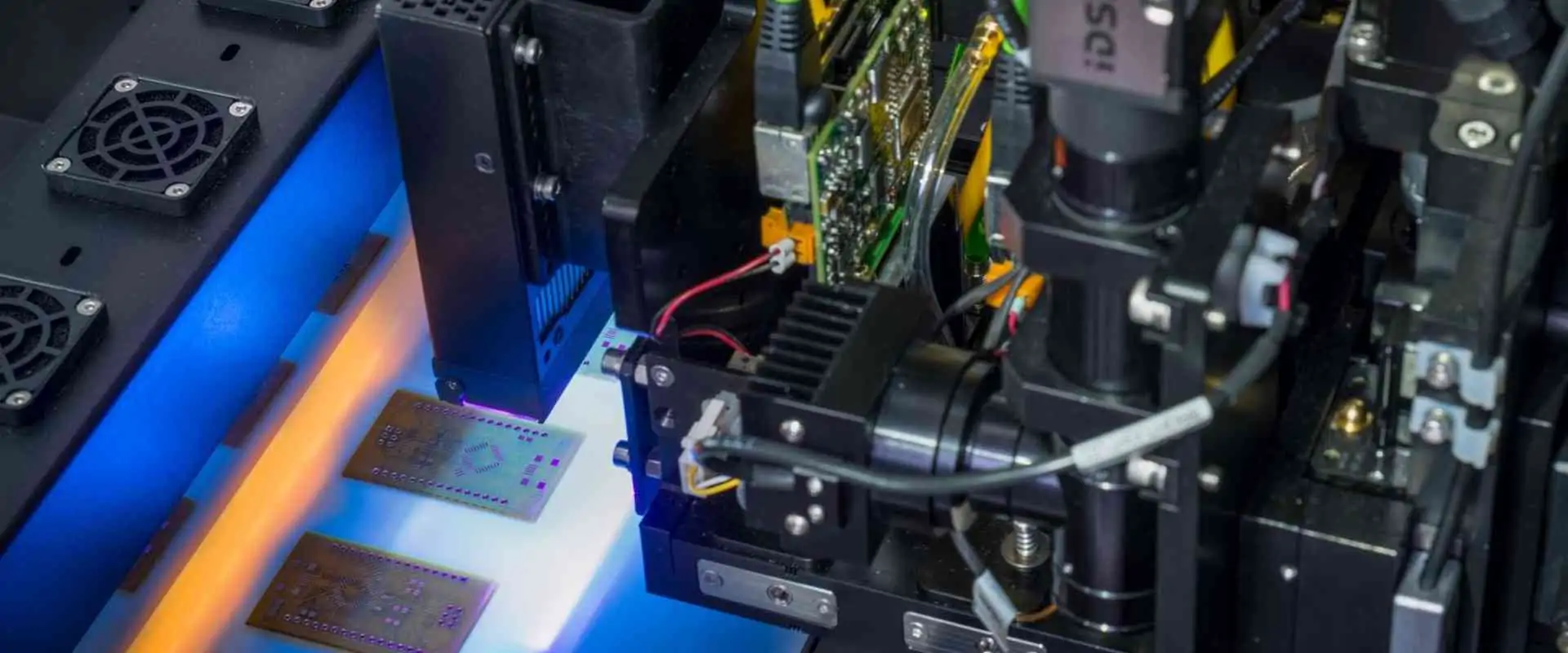
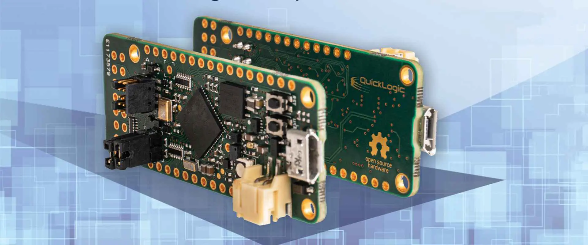
One of our favorite examples is QuickLogicโ€™s PolarPro Family. This series of products is a complete suite of tools that includes a multimedia computer running on Windows OS and several mobile apps for iOS and Android.

QuickLogic PolarPro Family history

QuickLogic PolarPro Family is a collection of products created by QuickLogic, a CPU, graphics, and peripheral IC supplier based in China. Since the company started operationsย in 2005, it has expanded rapidly and caters to many different market segments worldwide.

QuickLogic PolarPro Family consists of three different products: PolarPro V1.0 for Windows; PolarPro V1.0 for iOS; and PolarPro V1.0 for Android.

The first version of PolarPro V1.0, released in June 2010, was the original Windows version. QuickLogic followed up with mobile apps for iOS and Android in December 2015.

QuickLogic PolarPro Family is suitable for both consumers and developers. While the former group can use it to engage in the media and perform other day-to-day tasks on their PCs or electronic devices, developers like Rayming PCB & Assembly can use it to build new applications.

Perhaps the PolarPro V1.0 for iOS and Android can be helpful to develop a new application that lets users quickly look up information on the Web. For example, an app could tell travelers their location and directions. In addition, one can develop apps that

But with so many options, how do you know which product is right for you?

QuickLogic PolarPro Family overview

QuickLogic PolarPro Family for Windows

The QuickLogic PolarPro V1.0 for Windows is a multimedia computer that can run all the popular applications on the market today. In addition, it is a full-featured operating system that has all of the latest technologies, such as 3D graphics, photo editing, and other functions.

PolarPro V1.0 for Windows can perform Internet searches, read e-books, play games, download videos, edit images and other content, listen to music and voice recordings, and much more.

PolarPro V1.0 for Windows enables you to work with all types of multimedia content in high-definition 4K or 1080p resolution via HDMI or DisplayPort connectors. You can also connect a TV through an S-Video or composite port to view videos on it.

PolarPro V1.0 for Windows can be helpful in nearly all scenarios, from home to business, and even in professional settings where you need to use a computer for tasks such as designing software or photo editing.

The PolarPro V1.0 for Windows has several useful applications to help you accomplish various tasks easily. For example, you can listen to music by using the built-in music player and Internet browser to access websites.

QuickLogic PolarPro Family for iOS

PolarPro V1.0 for iOS comes preinstalled on mobile devices, along with an app store that enables you to download more apps as per your requirements and preferences. This enables you to browse the Web, manage e-mails, keep a record of your expenses, play games, and perform other tasks efficiently with just a few taps on your mobile device.

QuickLogic PolarPro V1.0 for iOS also comes with a virtual keyboard feature that lets you type and send messages without worrying about typing errors. Instead, the keyboard works as per your requirements by predicting the next word in a sentence and auto-correcting any mistakes you make while typing.

PolarPro V1.0 for iOS can be helpfulย on Apple devices such as iPhones and iPads, but it is not limited to these devices alone. You can use it on other iOS compatible devices that run OS 6.0 or higher.

What makes PolarPro V1.0 for iOS stand out is the wide range of benefits that it offers and its efficiency and simple-to-use interface. For example, we can do app downloads quickly and easily.

PolarPro V1.0 for Android

The QuickLogic PolarPro V1.0 for Android is also a multimedia computer that runs on Android OS. In addition, the software package comes preloaded on mobile devices such as smartphones and tablets.

Like PolarPro V1.0 for Windows, the PolarPro V1.0 for Android can take full advantage of the latest technologies. In addition, it has a user-friendly interface that makes it easy to perform common tasks such as playing games, watching videos, and listening to music.

PolarPro V1.0 for Android has various applications that let you download multimedia content from the Internet in just a few taps.

These apps also enable you to communicate with friends and family by sending them e-mails or voice messages. You can also use some of these apps to read books and magazines through the built-in reader app or play games on your mobile device.

PolarPro V1.0 for Android is compatible with devices that run Android 2.3 or higher and support OpenGL ES 2.0.

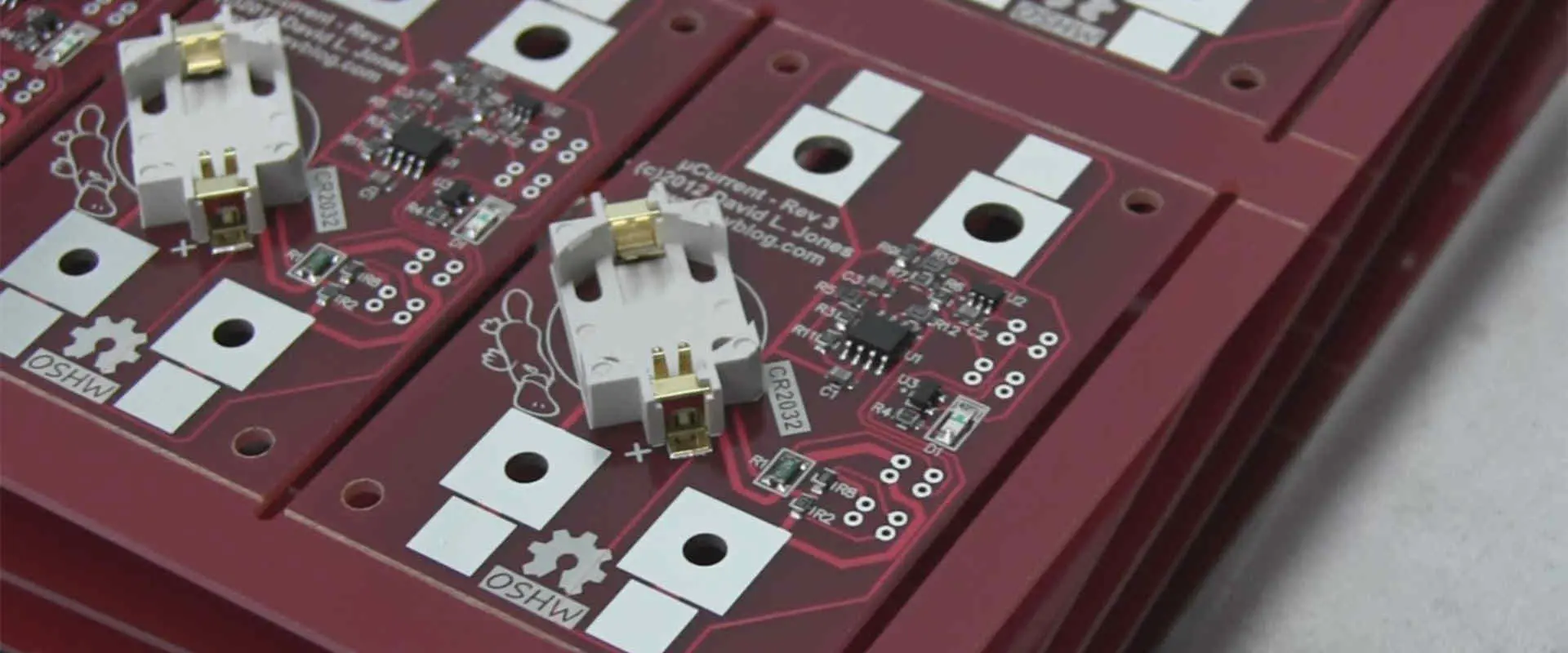
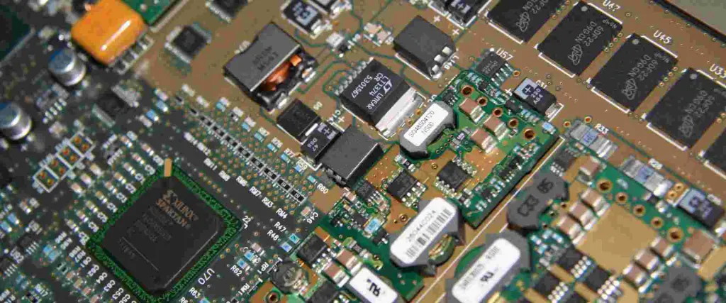
Critical features for the QL1P1000-6PS324C QuickLogic PolarPro device

1. Process Data

The QuickLogic QL1P1000-6PS324C is fabricated on a 0.18ยตm process technology and delivers a 2D performance of 2.7 million square pixels/second, processing data at 7.2 Gpixel/s and drawing 260 million triangles/second.

To deliver the reference 256MB of frame buffer memory, the PolarPro device provides 1 Gbytes of internal memory on-chip and interfaces to system memory through 2×64-bit DDR3 channels running at 800 MHz or 64-bit SDRAM running at 400 MHz.

PolarPro depends on a 0. Six-layer metal CMOS process, ensuring the scalability and reliability of the chip.

2. Programmable Logic Architecture

The QL1P1000-6PS324C contains programmable logic modules that support the power requirements for all system components, including processors, memory, and peripheral components. It is a single register, the multiplexer-based logic cell containing several programmable logic blocks arranged in a technique that allows reprogramming the logic to meet the system requirements.

The programmable logic architecture allows flexibility in the design of systems. In addition, the programmable logic can be helpful to offload specific tasks from processors, such as image processing, audio and graphics processing, scheduling, and some communications processing.

You will find high fan-in per component and high fan-out per package in our devices. The high fan-in per component is due to the flexible nature of the architecture and the flexible routing of interconnects.

3. RAM Modules

The PolarPro QL1P1000-6PS324C contains five DIMM slots and a single slot for memory cards. It draws power from the CPU through a multi-phase design that handles the voltage and current delivery to the RAM modules.

Each DIMM can handle two 64-bit DDR3 modules, accessing them through 72-pin SODIMM sockets.

The devices also provide redundancy by using redundant sockets, which allow data transfer to be interrupted by request while it is transferring data. Its features include:

a) Non-pipelined read data path: The PolarPro device can use all memory bandwidth even when using only a single module. This feature is also available in the clock domain.

b) Write byte enables: The CPU can write data directly from the buffer and use it as input for further computations. This feature also provides read-while-write support.

c) Vertical and horizontal concatenation: The device can combine vertical and horizontal data blocks into one transaction.

d) Independent read and write clocks: The device uses independent clock domains for read-data and write-data, respectively.

e)  Independently configurable r/w data bus widths: The read and write clock can be independently configured.

4. True Dual-Port RAM

In addition to its five single-ended RAM modules, the device also provides an actual dual-port RAM that supports two independent clocks, allowing additional processing. We implement the dual ports in the following:

a) Block data transfer from memory to memory: The RAM blocks may split into different sections for transfer between the two modules.

b) Multiplexed read and write accesses: Multiple reads and writes can occur simultaneously across all modules of the device. For example, it is possible to write to one memory section while reading from another memory location.

c) Single-cycle read and write access: The device performs a read or writes at a single cycle of the clock input. This feature allows various operating modes with reduced latency and power consumption.

d) Data transfer between two RAM modules: The device can access two distinct data sections in two separate RAM modules within the same clock edge. This feature allows DMA transfers with reduced latency and power consumption.

It is important to note that no circuitry prevents a write and read operation from happening simultaneously. So, this feature is true to the point that there is no memory access violation.

The physical architecture of the QL1P1000-6PS324C requires additional power to supply all the components. It includes a 200 MHz clock for all RAM modules, a 200 MHz clock for each dual-port RAM module, and a 100 MHz clock for the CPU.

5. Embedded FIFO Controllers

The PolarPro device contains embedded FIFO controllers used in sending and receiving data. The embedded FIFO controllers support the following features on the QL1P1000-6PS324C:

a) Different types of stream control: The FIFO controllers support different streams such as control registers and video processing.

b) In-order double-buffering: The device has two banks to handle updates to two different devices. This allows continuous data communication with reduced latency.

c)  Pipelined read data to improve timing: The devices have a two-stage pipeline that provides data at the output of the first stage and input to the second stage simultaneously. This reduces latency as well as power consumption.

d) Independent read and write clocks: The device uses independent clock domains for read-data and write-data, respectively, for each FIFO controller. These registers allow data synchronization in non-critical paths separately from critical paths to reduce latency.

e) 4-bit PUSH and POP level indicators: The push and pop FIFO registers have a 4-bit level indicator that shows the number of data bytes written to or read from the FIFO.

f) Configurable FIFO operation: The device is essential for synchronous or asynchronous operation for each FIFO. The synchronous and asynchronous modes have an independent write clock domain, read bus width, and bit-width.

g) Independent programmable data: The device supports independently programmable widths for all bytes pushed into the registers, and all bytes popped out of the register.

6. FIFO Flush Procedure

Both PUSH and POP domains come with dual-port RAMs. All data written to the FIFO controller is stored in a RAM when written into one port and then read out through the other port. The two ports connect using a single transfer bus, and this bus operates in two modes:

a) Transfer mode: In the transfer mode, data may move between two FIFO registers or between a FIFO register and memory. We treat two registers as one single 32-bit buffer in the transfer mode.

b) Read mode: Data from a single FIFO appears through a single port stored in RAM.

The flush procedure allows the devices to execute these functions without blocking other devices with minimal interference. It also supports simultaneous flushing of all FIFO domains to reduce latency and remove errors.

The DC input to all RAMs turns on when a flush is triggered and executes a flush cycle. The DC input to the FIFO controller is turned off at this point to avoid turning it on before the device has finished reading data from one of its ports. After an entire bus cycle has elapsed, the devices initiate an additional bus operation that puts all the RAMs back into their normal states.

7. Clock Network Architecture

To achieve its high performance, the device contains a clock network architecture designed to eliminate bugs in clock domains and reduce interference. A global unsynchronized differential clock operates at 200 MHz. All critical functions of the device depend on this clock. The global clock has six independent clocks at 100 MHz each, and they are distributed selectively to essential components of the devices.

Distributed Clock Networks:

It consists of a 3-level H-tree network. All six of the devices contain one H-tree network. The H-tree network has two clocks: primary and secondary clocks. The primary clock is helpful for critical operations, such as power and system initialization, configuration, RAM initialization, and debugging operations. The secondary clock is helpful for subcritical, such as interrupts, serial ports, and on-chip timers.

Dynamic Clock Enable:

Each clock network can automatically disable itself when not needed. When a network is disabled, the secondary clock in each node is also disabled. This feature allows the device to sleep and wake up quickly. This capability is used on each node to identify critical and non-critical nodes. For example, the power and system initialization domain are essential, while other domains are considered non-critical. Therefore, the power and system initialization domain will be enabled only when an external reset source drives the device into its active mode.

Configurable Clock Managers (CCMs):

The devices contain four 16-bit single-cycle CCMs used by the CPU to handle signals in each clock network. The CCMs vary the speed and phase of their clocks according to the incoming signals. For example, the input frequency could range from 10-150MHz. The output frequency could range from the input frequency to half of the input frequency. The conversion ratio is (1/2)n, where n = number of stages in the CM. The domain that controls the maximum frequency determines whether it is a critical or non-critical domain.

Simultaneously Switching Outputs:

The devices allow SSO and CM to work simultaneously. Since the SSOs require a longer time than a single cycle, the clocks with higher frequency may use the same output of a CCM. The nodes are capable of utilizing this capability to reduce DC power consumption. As shown in figure 1 above, six independent clocks operate in each device. These clock domains include:

i) VDEDAC: This domain provides the timing signals to control the operation of VDEDAC circuits on each pixel engine. It receives signals from the SCM and collation circuits. In addition, the VDEDAC circuit is responsible for delivering clocks to a few pixel engines.

ii) Clock Controller: The clock controller controls each clockโ€™s timing, frequency, and phase. It can switch between CCMs and their outputs or SSOs at any time without losing synchronization with VDEDAC and SCM. The clock controller monitors all the 16-bit single-cycle CCMs and, if needed, enables them to operate simultaneously. The following signals monitor the VDEDAC and SCM:

1) SDCB: We use this signal by the SCM to synchronize with VDEDAC.

2) SYNCB: SYNCB is a signal provided by the CAMP. The SCM uses this signal to implement synchronous operation with VDEDAC within a certain time scale.

8. GPIO Cell Structure

There are three main functional blocks in a GPIO cell: data latch, flip-flop, and output driver. The data latch is helpful to store data during transfer and check the dataโ€™s status. This block also receives signals from the SCM VDEDAC and outputs CCM current. We use the flip-flop to generate output control signals. It also receives input control signals from the CCM, SDCB, and SYNCB. Finally, the output driver controls current levels and output timing to meet each portโ€™s data transfer requirements. It also receives data from the data latch and supplies current to the load drivers according to the data from the flip-flop.

With global clock input pins and bi-directional I/O pins, this block can be helpful as a functional block and a communication interface. Each GPIO cell has three outputs and one input. The outputs are used for the data transfer and global clock input, while the input is essential for the data transfer from the host system and global clock output.

9. DDRIO Cell Structure

It allows clocking data on the negative and positive clock edges. The DDRIO adaptor block includes a finite state machine and a flip-flop. The flip-flop stores data to control output signals. There is one output for each port of the device. Depending on whether the port needs to transfer data, the corresponding outputs will be disabled or enabled using the input/output control signals from CCM. You can configure the I/O using the configuration mentioned earlier tools.

10. Very Low Power Mode

It is a mode to reduce power consumption beyond the deviceโ€™s dynamic power reduction mechanisms (clock gating, power, system initialization domains, etc.). In this mode, application modules in the device turn off when they do not need using at a particular time. It reduces power consumption by about 30 percent compared with non-sleep mode. In addition, they can bring the standby current to below 10 ยตA.

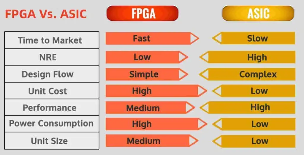
The main advantages of employing FPGA are customization, low power consumption, and flexible circuit layout. But like most other methods of IC design, the FPGA technology is not perfect, as it involves higher costs and lower performances compared with digital circuit design at a certain level of integration. In addition to that, each time an FPGA needs to be modified or debugged, it must burn. Quickly building the hardware circuit is one of the advantages of FPGA technology. But once you have built your design, it will be challenging to change it. After the burn-in test, you can only modify the existing hardware circuit layout or add new functions to your hardware circuit.

11. Joint Test Access Group (JTAG) Information

JTAG signals are not common to all FPGAs. To ensure the correct operation of the QL1P1000-6PS324C devices, you must use JTAG signals for testing and debugging purposes. The JTAG connector is located under the circuit board and can connect with a JTAG debug board (JDR-4X4 or similar type). There are two types of pins: negative test pins and positive test pins, each helping the corresponding PCB side. QL1P1000-6PS324C devices operate in the following test modes: soft reset and hard reset.

The QL1P1000-6PS324C devices have a serial debug port (SPORT) that can help conduct device mode-independent debugging. The SPORT is attached to the JTAG port of the QL1P1000-6PS324C PCB.

a)  Bypass Instruction: The host computer can access all the deviceโ€™s resources in bypass instruction mode. All packages are accessible except for those locked into lower power consumption states. This mode is helpful to check the deviceโ€™s operation, monitor signals, and check variablesโ€™ values.

b)  Sample/Preload Instruction: This helps access the deviceโ€™s memory space. The target addresses of data, control, and address bytes move via a JTAG (serial) link to the QL1P1000-6PS324C device.

c)  Extent Instruction: This helps access the deviceโ€™s internal logic. If a fault occurs during the test procedure, the device will send an error code to the host computer. This mode can debug your design when you are using JTAG signals.

12. Electrical Specifications

In order to provide its users with the best performance and highest reliability, the QL1P1000-6PS324C device has the following specifications:

1) VDEDAC :

a) Input Voltage: +5 Vpp to +15 Vpp

b) Output Voltage: 0.8 Vpp to 2.4 Vpp

c) Operating Temperature: – 40 ยฐC to +85 ยฐC (ยฑ0.5ยฐC)

d) Package Type: QFP-80P

2) CCMO :

a) Output Voltage: 0.8 Vpp to 2.4 Vpp

b) Operating Temperature: – 40 ยฐC to +85 ยฐC (ยฑ0.5ยฐC)

c) Package Type: SOT-23-3

3) RPU :

a) Output Voltage: 0.8 Vpp to 2.4 Vpp

b) Operating Temperature: – 40 ยฐC to +85 ยฐC (ยฑ0.5ยฐC)

c) Package Type: SOT-23-3

4) PLL :

a) Operating Voltage: 4.75 Vpp to 5.25 Vpp

b) Frequency Range: 790 MHz; 800 MHz; 860 MHz; 900 MHz; 950 MHz; 1000 MHz.

Conclusion

 In conclusion, the PolarPro Devices QL1P1000-6PS324C provides a wide range of memory and FIFO-related functions that can help develop complex applications. The device is specifically suitable for video processing and graphics applications that require high data bandwidth. The PolarPro QL1P1000-6PS324C RAMs are ideal for any application that requires fast access to high-performance data.

What is a Printed Wiring Board (PWB)

Shengyi ST115G PCB

The electronics field is intricate, whereby different phenomena happen in this field. Making use of acronyms and abbreviations, most especially those with three letters could become an issue to professionals and students in that field as this could cause some confusion.

PWB is similar to PCB and both are commonly used when it comes to the electronics designing and production field. Therefore, it becomes necessary to know the differences between the two.

In this article, we will be considering what printed wiring boards are, which is our focus. Then we will discuss the major factors affecting the way printed wiring boards perform. Lastly, we will focus on the differences between the printed wiring board and printed circuit board.

If you wish to gain full knowledge regarding this topic, please stay on this page, we promise to explain in detail all you need to know.

What are Printed Wiring Boards?

Printed wiring boards, just like the printed circuit boards are very important for all electronic devices. They were introduced back then in the early 1950s. This served as the building block for any electronic packaging.

One important feature of a printed wiring board is getting the highest components count for each square inch of printed wiring board (PWB). We call this component density. Therefore, a good number of packaging techniques came to be. These include Chip on Board, Chip Scale Packaging (CSP) and Ball Grid Array.

Furthermore, the components of the surface mount have a miniature size. Also they are used extensively in the majority of printed wiring boards. This offers maximum density of the component, coupled with providing some maintenance for the thermal, electrical, and the signal integrity of the device.

Also present are different materials which are useful for the PCB substrate. Notably, FR4 is the most commonly used.

What are the Major Factors Affecting the Way Printed Wiring Boards Perform?

The way printed wiring boards perform can be affected. Below are the main factors.

The Printed Wiring Boardโ€™s Speed of Operation

One important factor in printed wiring boardโ€™s interconnection design is the speed of operation of electronic devices. Also, the speed of signal proportion has an inverse proportion to the Dk (dielectric constant) of the printed wiring boardโ€™s substrate material.

Furthermore, the time of flight is known as the propagation time of the signal, which has a direct proportion to the conductorsโ€™ length and has to be kept completely short of making sure that a systemโ€™s electrical performance is kept at an optimum. When higher than 25MHz, printed wiring boards (PWBs) make use of the micro-strips and strip-lines to achieve this purpose.

The Power Consumption of the Printed Wiring Board

Increasing the gates number, as well as clock rates will lead to an increase in the consumption of power. You must take great care for switching circuits of high speed where current flow of ground return is optimally channeled. In addition, there must be a separate or different ground plane in multilayer printed wiring boards (PWBs). This is mainly to ensure that there is a current flow of low resistance. Furthermore, thereโ€™s a need for a bus bar system made different. Also, this is preferable for circuits of high power.

Thermal Management

Printed wiring boards are poor heat conductors. Therefore, you must take proper care when using the methods for the dissipation of the heat that has been generated by the printed wiring boardโ€™s power consumption. Metal slugs, as well as conductive planes, heat vias, heat sinks in printed wiring boards, are very good techniques.

PWB vs. PCB: What are the Differences?

The differences between printed wiring boards and circuit boards are outlined below:

Components

During the comparison of the Printed wiring board and printed circuit board, one of the most obvious and important differences is that the printed circuit board (PCB) has to do with a board having the entire circuitry. While Printed Wiring Boards have to do with a board that has no components.

What this means is that PCBs are already completed circuit boards. They are set for installation in electronic devices. Furthermore, PWB helps in indicating the rudimentary circuit board production. Also it shows the usefulness of a circuit board in electronics, which doesnโ€™t need complex functionality.

Area and Location

Both words are used in different ways depending on the area and location. Take for example, with respect to the United States of Americaโ€™s industry for electronics production, they can interchange both terms.

Printed Wiring Board was the term used back then. This was a time when the electronics world was still in the infant stage. All through the beginning time of the industry, printed wiring boards were deemed fit as the right name or term due to the connections present on the boards that were majorly from just a point to the other.

Later on, printed circuit boards were introduced when there was a great advancement in the levels of the technology of circuit boards. At first, restriction was placed on this compound noun for internal use alone; circuit as a term was very useful as the printed circuit board provided extra complex functions.

Moreover, with the great advancements in technology, PCB got to the whole population, which has now restricted printed wiring boards (PWBs) to the preproduction of electronics.

Printed wiring boards are known as the design substrate having no component attached to it. Asides from its etching bit, printed wiring boards also feature openings. This allows the soldering in of electrical components, as well as through them.

Asides from the fitting of electrical components, printed wiring boards have to go through some physical and chemical processes before they become finalized into printed circuit boards.

This came from printed circuit board design, which plays a huge role in the functionality of the course.

Conclusion

This is the end of our article on printed wiring boards. We have been able to explain what it is. We also explained how it is different from the printed circuit boards. If thereโ€™s any aspect of the article where you need more clarification on, please feel free to drop your questions. We have experts in the field that are ready to help you out.

What is the Purpose and Applications of a PCB Motherboard

PCB Motherboard

A PCB Motherboard is useful in most electrical appliances of today. This is one good reason why it is important that you understand the details concerning them. This will help you choose the very best to work with your application.

We have written all the necessary points you should know regarding PCB motherboards for you to understand. We advise you read this article properly in order to have the necessary information about the PCB motherboard, coupled with solutions to all your questions.

What is a PCB Motherboard?

A PCB motherboard is built to have several layers. What this means is that its traces are usually run in at least four levels. Furthermore, they have many different connectors, passives, and chips.

PCB motherboards which can be sometimes called the planar board, system board, logic board, or main board is the major PCB that is seen in computers, as well as other systems that are expandable.

PCB motherboard does a great job in holding and allowing communication to happen between many important electronic components present in a system like the CPU and the memory. Furthermore, it offers communicators for some other peripherals.

In contrast to the back-plane, the motherboard is made up of a huge sub-system like the processor, as well as other components.

PCB Motherboard Design

A PCB motherboard offers the right electronic connections through which the systemโ€™s components communicate. In contrast to the back-plane, the motherboard also includes the CPU (central processing unit) as well as other devices and subsystems.

Typically, desktop computers feature a main memory, microprocessor, as well as other important components that are connected to the PCB motherboard.

 Some other components like external storage, and controllers for sound and video display, as well as peripheral devices can be somehow attached to your PCB motherboard via cables or plug-in cards. In today’s computers, it has become very common to incorporate a number of the peripherals into your pcb motherboard.

One significant component of PCB motherboards is the supporting chipset of the microprocessor. This is known to offer support to the interfaces in-between the central processing unit and the different buses, as well as external components. The chipset helps in determining the capabilities and features of the PCB motherboard.

Does PCB Motherboard and PCB Mean the Same Thing?

In computers, motherboard pcbs are known to perform similar functions as the printed circuit boards found in any electrical appliance.

Printed circuit boards are useful in the manufacturing of laptops and desktop computers. Also, they ensure the use of some internal components present in computers like video cards, expansion cards, controller cards, etc.

This motherboard, also referred to as the printed circuit board is the place where all the components are all connected. Although motherboard computers have a link with computers, they are also useful in different electronic devices excluding computers.

Tablets, smartphones, digital cameras, radios, and televisions usually have at least one PCB motherboard. All PCB motherboards can serve as PCBs. Moreover, not all printed circuit boards can serve as motherboards.  

What Purpose does a PCB Motherboard Serve?

An electronic circuit that is discrete is usually created on a PCB motherboardโ€™s foundation. It plays a huge role in offering all the traces of the circuit, which has been developed already in between these electronic components after a specific assembly.

Pads that are electrically conductive made of plated through holes or copper, are useful for attaching an electronic component on the PCB motherboard.

The copper lines which connect the holes and pads are etched between the fiberglass layers or on the boardโ€™s back and front surfaces. This depends on the motherboardโ€™s PCB design. This copper line route establishes the electrical connections that are necessary between these components.

Applications of the PCB Motherboard

PCB motherboards are useful in these applications.

Electronic Television

PCB motherboard is important here to make sure that your televisionโ€™s electrical circuits and components stay connected. This means that your television will have a stable performance.

LED Projector

LED projector PCB motherboards are new inventions, which have unique features as projectors produce light to perform well. It also functions differently from other forms of electrical appliances in use.

Therefore, LED projector PCB motherboards stand out in its applications and characteristics.

Smartphone

PCB Motherboards are useful in smartphones which have a similar appearance to those present on desktop computers as well as electronics that are heavy, though they seem to have a smaller size and have finer circuitry compared to others.

Keyboard

Keyboard PCB Motherboards are usually composed of platinum. Furthermore, it is known as the most sensitive compared to other applications. You have to prevent it from coming in contact with weight and water.

Choosing a Reliable Processing Factory for Your PCB Motherboard

It is very necessary to conduct proper research concerning the PCB motherboard processing factory you want to patronize. Make sure you check the reviews of some manufacturers then work with those having good reviews.

You can then make your choice with respect to any of those manufacturers that meets these requirements.

Rate of production

If you wish to perform the processing of a PCB motherboard, work with a company possessing all the necessary equipment, coupled with the appropriate rate of production. Once you have assessed the production rate, as well as equipment quality of this manufacturing firm, you will easily tell if they are strong enough.

Quality Control and Assurance

A reliable PCB manufacturer will never allow defective PCB motherboards to get to the market. Top manufacturing firms always place great value on the maintenance of quality control all through the processing and manufacturing stages.

Quality of Customer Service

Top manufacturing firms are known not just for their great quality when it comes to production, but the status also depends on the quality of the customer service.

This company must have a great staff coupled with business professionals with vast experience that responds very quickly to different issues.

Conclusion

We hope that with this article, we have been able to provide answers to all your questions concerning PCB motherboard. If there are more questions for us, you can reach us here.

All about SMD/SMT and what they entail

smd smt

Surface Mount Technology (SMT) and Surface Mount Devices (SMD) considerably speed up the PCB assembly process. Instead of using traditional means of electronic assembly, which features the use of wire lead and huge components. Manufacturers are now leaning onto minute components to save cost and produce electronic devices in bulk.

If you open up any modern-day commercially made device, you will note that most if not all of its components are minute. So how is this possible? Well, that is where SMT and SMD come in. SMD and SMT allow manufacturers to mount minute components onto PCBs. In doing so, they save on cost and utilize less time in the manufacturing process. In that case, you get commercial electronics that are cheap, compact, and that function incredibly. But what exactly does SMD/SMT entail? Why are they useful? And what are the differences between the two? To find out more, follow along and let us unravel this mystery.

SMT

Surface mount technology (SMT) is simply a new tech design manufacturers use to arrange various components printed onto a PCB. Previous mounting versions were not as effective as SMT due to the use of holes to mount components. These traditional methods require careful preparation to ensure that all the lead you use fits various PCBs. The leads should also form the correct technique. It also needs a relatively larger PCB that can fit more than one circuit.

However, using SMT machine, the PCB assembly process becomes pretty efficient. That’s because you solder various components onto the PCB directly. Also, this impressive technique doesn’t require you to pass leads through your PCB. It is hence:

  • Simple
  • Efficient and,
  • Cost-effective

What’s more, SMT saves you a lot of space as you can mount components on both sides of the board. Moreover, you get to accommodate many components on a single PCB in so doing.

Therefore if you sometimes wonder how compact components pack great features nowadays. Then now, you have the answer; it is all about space utilization in the best way possible.

When working with a minute component, the error probability goes up. However, that is not a huge issue with SMT since you can easily fix errors using molten solder. In traditional methods, fixing errors was complicated and lengthy. However, with SMT, you face low wire attachments, and you do not have to drill holes onto the PCB, which saves you a lot of stress.

What is even more fascinating about SMT is that it features little to no lead making it eco-friendly. It also has solder joints and primary components on the same side of the PCB.

Features of SMT

  • Components have short leads or ultimately no leads
  • Solder joint and the components for the main body lie on the same PCB side

SMD

Surface mount devices (SMD) are the various components you find fitted onto a PCB. These components are pretty ideal in an era whereby people are looking for devices that are:

  • Cost-effective
  • Flexible
  • Faster

These features are what’s making SMD evolve and gain popularity pretty fast.

Previously, manufacturers were wiring SMDs onto various circuit boards, but now things have taken a turn. Modern-day SMDs come with pins that manufacturers use to solder them onto PCBs, making the entire process pretty easy.

With SMDs, tiny components can ensure that you achieve functionalities that equal the use of larger components. If so, then these components do not just save on space. They are also more functional. All these make it possible to place more circuits on a single board, and since you do not have to drill PCBs, the process becomes:

  • Fast and
  • Cost-effective

What’s more, SMDs also provide:

  • Fewer RF signals effects which are unwanted
  • Higher frequency performance

Since SMDs are tiny and easy to use, they are also cheaper than traditional SMDs, which need holes for installation. Hence utilizing SMD/SMT saves you more than you can even imagine. A combination of this two brings in a new era of technology.

SMD features

  • Miniaturization
  • Great for PCB surface assembly
  • No lead (short or flat lead)

SMD Types

Chip resistor

Chip resistors have three digits which you can find on the body of the chip resistor. These three digits show the chips resistance value.

Net Resistor

Network resistors are packages that have a couple of resistors in one parameter. Digital circuits use this feature extensively.

Capacitors

As of the 21st century, you can only find two standard capacitors in the tech market:

  • The Tantalum capacitors
  • The Aluminum Capacitor

You, however, need to clearly distinguish between the two’s polarity.

Diode

Diodes are pretty popular in the SMD world. As a result, manufacturers working with SMD/SMT highly utilize diodes in their projects.

LEDs

Two classes of Light Emitting Diode (LEDs) exits.

  • Ordinary LEDs
  • LEDs having high brightness, for example, blue, red, yellow, and white

You should also note that manufacturing guidelines determine LED polarity.

Transistors

Mostly, transistors are either:

  • NPN or
  • PNP

They can also be either be:

  • Crystal Oscillators
  • Fuses
  • Transformers
  • Inductors

IC

Integrated circuits are pretty important functional components of electrical products. Moreover, ICs are pretty complex and efficient, making them appropriate for SMD/SMT processing.

SMT VS SMD

SMT utilizes mounting tech to mount and solder components onto PCBs. On the other hand, SMD refers to the use of various components that manufacturers mount onto PCBs using SMT tools. In addition, the SMD technique utilizes components that manufacturers solder onto PCBs using soldering paste.

Commercial manufacturing of electronic devices utilizes SMT as it is cost-effective. By using SMTs, manufacturers get to provide electronic devices to you as the client in a cost-effective manner.

SMT also offers stronger bonds ideal for various components built under stress.

Where SMD and SMT combine

Manufacturers use SMD/SMT in the PCB assembly process, and hence if you wish to tackle a similar problem, you should follow the same plan. However, the technique you will use greatly depends upon the material you will be using.

Another important thing to note is that you should always use the proper gadgets to get the right results. Utilizing the wrong tools has catastrophic results, which you do not want.

Conclusion

Tech advances every day, and so does how things function in the tech industry. A change in how components connect onto PCBs is one area that has undergone great changes. These changes have brought about faster manufacturing of compact electronic devices. Therefore, now we have many tiny smartphones that work better than the tall telephone booths from the 90s. Hence, for the question “is SMD/SMT necessary in the 21st century?” we would say, yes, pretty much.

How Does a Temperature Sensor Work?

temperature sensors

Temperature sensors are one of the most widely used sensors across various applications such as consumer electronics, automobiles, industrial equipment, IoT devices, and more. They allow monitoring and controlling temperature which is a key parameter affecting performance, safety and reliability.

This article provides a comprehensive overview of the inner workings of various types of temperature sensors. We examine the underlying sensing principles, signal conditioning circuits, packaging considerations and output interfacing for common temperature sensor technologies.

Temperature Sensor Types

Different physical effects utilized by sensors to determine temperature:

Thermocouples – Measure voltage generated due to junction of two dissimilar metals

RTDs – Measure change in electrical resistance of metal element

Thermistors – Utilize semiconductor material’s resistance variation with temperature

IC Sensors – On-chip amplification and conditioning converts voltage/current into digital output

Pyrometers – Measure infrared energy emitted by an object

Bimetallic – Physical deformation of two bonded metals with different expansion coefficients

Thermocouple Temperature Sensors

Operating Principle

Thermocouples rely on the Seebeck effect – generation of voltage due to a temperature gradient along the junctions of two dissimilar metal wires. Common types:

  • K type (Nickel-Chromium and Nickel-Aluminum)
  • J type (Iron and Constantan)
  • T type (Copper and Constantan)
  • E type (Nickel-Chromium and Constantan)

The voltage generated is proportional to the temperature difference. Reference junctions provide cold junction compensation.

Structure

Thermocouples have a simple structure with two wires made of specific alloys joined at one end to form the hot junction. This junction is brought in contact with the target being measured while the open wire ends connect to the measurement system.

Working

When the hot junction experiences a temperature change, a voltage difference is created which causes current to flow through the loop. This voltage is linearly proportional to the temperature gradient. The reference junction provides a baseline cold temperature reading. The system measures and amplifies the small voltage signals in the microvolt range.

Characteristics

ParameterCharacteristic
Operating range-200ยฐC to 2320ยฐC
Accuracy0.5ยฐC to 1ยฐC
Response timeMedium (~200 ms)
CostLow
ProsHigh temperature range, low cost
ConsLow voltage output, noise pickup

Applications

  • Industrial processes running at high temperatures
  • HVAC and refrigeration systems
  • Automotive under-the-hood monitoring

RTD Temperature Sensors

Operating Principle

RTDs or Resistance Temperature Detectors operate on the principle that metals change electrical resistance linearly in proportion to temperature. RTD elements are made of metals like platinum, copper or nickel.

Structure

RTDs contain a fine coiled metal wire encapsulated within a ceramic or glass tube. The entire assembly is enclosed in a protective sheath for mechanical stability. Leads connect the coil to the measurement system.

Working

As the sensing element is subjected to a temperature change, its electrical resistance varies predictably. This change in resistance is measured using a Wheatstone bridge circuit. The variation follows a positive temperature coefficient (PTC) curve. Platinum shows near ideal linearity across a wide range.

Characteristics

ParameterCharacteristic
Operating range-200ยฐC to 850ยฐC
Accuracyยฑ0.1ยฐC to ยฑ0.3ยฐC
Response timeSlow (~10 sec)
CostMedium
ProsExcellent linearity and stability
ConsFragile, slower response

Applications

Thermistors Temperature Sensors

Operating Principle

Thermistors are thermally sensitive resistors made from semiconductor materials like oxides of manganese, nickel or cobalt. Their resistance changes exponentially with temperature as per the material’s unique curve.

Structure

They contain a sintered semiconductor material pellet or chip encapsulated in epoxy, glass or metal housing with lead wires. Different housing styles are available like beads, probes, discs etc.

Working

Thermistors have a large negative temperature coefficient (NTC) implying their resistance decreases rapidly with increase in temperature. The nonlinear change is measured by passing a current and determining the voltage drop. No amplifier is required to condition the output.

Characteristics

ParameterCharacteristic
Operating range-50ยฐC to 300ยฐC
Accuracy0.1ยฐC to 1ยฐC
Response timeFast (<5 sec)
CostVery low
ProsInexpensive, fast response
ConsLimited range, nonlinear

Applications

-Automotive sensor circuits

IC Temperature Sensors

Operating Principle

Integrated circuit sensors incorporate amplification, analog-to-digital conversion, compensation and calibration on-chip to provide fully conditioned digital temperature readings.

Different sensing mechanisms are utilized:

  • Voltage difference of diode junctions (silicon bandgap)
  • Change in base-emitter voltage (VBE) of BJT transistors
  • Variation in mobility of charge carriers within transistors

Structure

IC sensors come in tiny surface mount packages like SOT23 containing the silicon microchip. Leads provide power and digital interfaces like I2C/SPI.

Working

The raw on-chip sensor converts temperature into corresponding voltage or current. Support circuits amplify, linearize, digitize and calibrate the signal. The microcontroller interface allows easy integration.

Characteristics

ParameterCharacteristic
Operating range-55ยฐC to 150ยฐC
Accuracyยฑ0.25ยฐC to ยฑ2ยฐC
Response time<500 ms
CostLow
ProsDigital output, fast, integrated
ConsLimited range, power consumption

Applications

  • Smartphones, tablets, laptops
  • IoT and wearable electronics
  • Drones and robotics
  • Smart home automation
  • HVAC and weather stations

Infrared Pyrometer Temperature Sensors

Operating Principle

Pyrometers calculate temperature by detecting the infrared radiation emitted by an object based on its emissivity. They work on the principle that hotter surfaces emit higher infrared energy.

Structure

Pyrometers contain a lens to capture infrared, spectral filter, infrared detector and signal processing circuits. The housing includes a sighting scope for aiming at the measurement target.

Working

The infrared radiation emitted passes through an optical window and is focused onto the detector. The photonic energy generates current that gets converted into voltage and amplified. Calibration curves compensate for emissivity variance.

Characteristics

ParameterCharacteristic
Operating range0ยฐC to 3000ยฐC
Accuracyยฑ1ยฐC
Response timeVery fast (10 ms)
CostMedium
ProsNon-contact, very fast response
ConsEmissivity dependence, distance

Applications

  • Monitoring high temperature surfaces like molten metals
  • Glass and plastic manufacturing
  • Furnaces and kilns
  • Welding monitoring

Bimetallic Temperature Sensors

Operating Principle

Bimetallic strips convert temperature into mechanical deflection by exploiting the different thermal expansion coefficients of bonded metals. Common material pairs are brass-steel and invar-steel.

Structure

They contain two thin strips of dissimilar metals joined together. The bonded assembly is shaped into a coil spiral for enhanced movement. The free end has an indicator, switch or potentiometer.

Working

When heated, one metal expands more than the other causing the bi-metal to bend. The mechanical displacement is proportional to the temperature change. This motion can toggle switches or move a wiper over a resistive element to produce an electrical signal.

Characteristics

ParameterCharacteristic
Operating range-20ยฐC to 150ยฐC
Accuracyยฑ3ยฐC
Response timeSlow (~60 sec)
CostVery low
ProsInexpensive, simple
ConsLow sensitivity, mechanical

Applications

  • Water heaters and cooking appliances
  • HVAC thermostats
  • Automotive engine monitoring
  • Irons, kettles and coffee machines

Temperature Sensor Signal Conditioning

Sensor output signals require conditioning before feeding to instrumentation. Common conditioning circuits:

Linearization

Linearizes nonlinear sensor outputs like in thermistors for consistent readings over full scale. Done using op-amps, A/D converters and linearization equations.

Amplification

Amplifies small sensor voltages up to usable levels. Important for thermocouples. Uses instrumentation amplifiers to minimize noise.

Filtering

Removes noise through low pass filters. Prevents aliasing errors in subsequent digitization.

Digitization

Analog to Digital Converters (ADCs) convert conditioned sensor voltage into digital values proportional to measured temperature. Provides interface to processors.

Calibration

Applies correction factors to eliminate sensor inaccuracies over temperature range. Done by characterizing sensor behavior and supplying coefficients.

Output Interfacing

Standard serial interfaces like SPI, I2C provided for connecting to microcontrollers or networks.

Temperature Sensor Packaging

Packaging plays an important role in:

  • Protecting the sensing element from environmental damage
  • Preventing contact with measured medium
  • Allowing rapid response to temperature changes
  • Isolating sensor electrically and thermally
  • Enabling straightforward integration

Common packaging types:

Plastic housing – Low cost, lightweight, resistance to chemicals

Ceramic casing – Withstands high temperatures, inert to chemicals

Metal sheaths – Robust protection in fluid applications

IC packagesSMD styles like SOIC, SOT-23 easy to integrate

Specialized probes – Shapes optimized for specific uses like air, surface and penetration

Temperature Sensor Selection Criteria

Factors to consider when selecting a temperature sensor:

  • Measurement range required
  • Desired accuracy and repeatability
  • Speed of response
  • Size constraints
  • Measurement environment – heat, humidity, pressure etc.
  • Electrical characteristics – analog vs digital output
  • Integration requirements – conditioning circuits, interface etc.
  • Application operating conditions – vibration, shock, EMI etc.
  • Compatibility with processing system
  • Calibration needs
  • Cost considerations

By carefully weighing these aspects, the optimal temperature sensing solution can be identified for any application need.

Common Temperature Sensor Applications

Temperature sensors find ubiquitous use across industrial, commercial and consumer applications:

Process monitoring – Chemical plants, oil refineries, pharmaceutical equipment etc.

HVAC/R – Air conditioners, heaters, thermostats, refrigerators etc.

Automotive – Engine control units, cabin climate control etc.

Consumer electronics – Mobile phones, computers, home appliances etc.

Medical – Diagnostics equipment, sterilization systems etc.

Food/chemical – Food processing, chemical synthesis, cold storage etc.

IoT – Smart devices, wireless sensor networks etc.

Frequently Asked Questions

What is the main difference in working of RTD and thermocouple?

RTDs measure temperature by change in electrical resistance of the sensor element while thermocouples generate voltage based on junction of two dissimilar metals.

How does emissivity affect pyrometer sensors?

Emissivity is a material property defining how efficiently it emits infrared energy. Pyrometers need to be calibrated for target emissivity for accurate non-contact temperature measurement.

Why are linearization circuits required for some temperature sensors?

Sensors like thermistors have an inherent nonlinear relationship between temperature and electrical parameters. Linearization converts this to a linear scale for consistent measurements.

What are the main considerations in temperature sensor packaging?

Important packaging considerations are protection from environment, fast response time, isolation from measured medium, robustness for the application, integration with electronics and cables/connectors.

What are some key selection criteria for choosing a temperature sensor?

Important parameters are measurement range, accuracy, speed of response, size, measurement environment, electrical interface type, application operating conditions, calibration needs and costs.

ASIC vs. ASSP vs. SoC vs. FPGA โ€“ What’s the Difference?

SoC FPGA and ASIC

Integrated circuits are essential building blocks powering nearly all modern electronic systems. Various semiconductor devices offer different capabilities and tradeoffs between factors like performance, development cost, and flexibility.

Key categories of ICs include Application-Specific ICs (ASICs), Application-Specific Standard Products (ASSPs), System-on-Chips (SoCs), and Field Programmable Gate Arrays (FPGAs). This article contrasts the key differences between these IC implementation approaches and provides guidance on selecting suitable options for electronics projects.

ASIC Overview

SoC FPGA and ASIC

An Application-Specific Integrated Circuit, or ASIC, is a custom silicon chip designed and manufactured for a particular application or function. Some defining traits of ASICs include:

  • Fully customized to requirements with tailored circuits
  • Very high performance since logic is hand-optimized
  • Long development time and high non-recurring engineering costs
  • Manufactured by semiconductor foundry
  • Amortize high upfront cost over volume production

ASICs harness the full power of integrated circuit fabrication technology, packing up to billions of transistors tailored for target applications onto silicon dies less than a square inch. Functions consolidated into ASICs span digital logic, analog interfaces, memory, custom processors, sensors, and mixed signal processing.

Since ASICs are fully designed from the ground up, they entail extensive engineering investment but achieve maximum density, performance, and power efficiency implementing desired functions in silicon. High volume consumer products like smartphones or IoT edge nodes benefit most from custom ASIC solutions.

ASSP Overview

While ASICs target a single specific application, Application-Specific Standard Parts (ASSPs) provide common integrated circuit functions useful across a range of systems. Some key ASSP traits are:

  • Standard IC products designed for broad applicability
  • Integration improves cost/power/size versus discrete solutions
  • Shorter time to market since designs are ready-made
  • Limited customization; tailored through external components
  • Lower volumes than ASICs; niche vs. mass market

Rather than invest in fully custom ASIC development, ASSPs provide integrated circuits addressing common needs that can be adopted off the shelf with some customization through external passive components, programming, and software drivers.

Examples include codecs, graphics processors, microcontrollers, physical layer transceivers, power management ICs, sensors, wireless radios, and many more. ASSPs are widely used to add intelligence and reduce component count in consumer electronics, IoT endpoints, industrial equipment, automotive, aerospace, medical products, and other embedded systems.

SoC Overview

A System-on-Chip (SoC) integrates multiple functions onto a single silicon die, similar to ASSPs but with greater focus on customer-specific system consolidation. Attributes of SoCs include:

  • Complete electronic system integrated into one IC
  • Can blend digital logic, analog, memory, processors, etc.
  • Extensive incorporation of IP building blocks
  • Closer to ASIC than ASSP regarding customization
  • Innovation enabler for product miniaturization

SoCs enable fully integrated single-chip solutions tailored for target applications. A smartphone SoC might pack CPU cores, graphics, cellular radios, accelerometers, and other components previously implemented with many discrete ICs.

This system consolidation is achieved by extensive intellectual property reuse. Various processor cores, interface blocks, and subsystems are integrated like LEGO bricks to match requirements while minimizing expensive custom logic.

SoCs occupy a middle ground between ASSPs and full custom ASICs. Their application-optimized integration can enable product breakthroughs by packing entire small electronic systems onto single cost-effective ICs.

FPGA Overview

Field Programmable Gate Arrays (FPGAs) offer an IC alternative maximizing flexibility and rapid prototyping by making logic gates and routing programmable using software. Key FPGA traits are:

  • Reconfigurable logic gates and routing
  • Programming allows implementing custom hardware functions
  • Faster bring-up compared to ASICs with reduced NRE
  • No high upfront fabrication costs; sold off the shelf

This reprogrammability makes FPGAs ideal for lower volume products that demand flexibility or require hardware upgradeability. Their architecture is also suited to hardware acceleration and high performance computing applications using inherent fine-grained parallelism.

While not reaching the density or performance limits of fixed-function ASICs, FPGAs empower agile development with reduced costs and risks. Programming follows a structured design flow from concept through synthesis, place and route, and configuration bitstream generation.

Development Process Comparison

These IC alternatives follow very different development processes and economics:

ASICASSPSoCFPGA
Design StyleFully CustomFixed FunctionMix of Custom and IPConfigurable Fabric
Process45nm – 7nm node28nm – 180nm5nm – 65nm16nm – 28nm
Typical Gate Count10M – 5B50K – 1M5M – 2B100K – 5M
Development Time24+ months6-12 months12-36 months3-12 months
Mask Cost$2M – $5M$500K$1M – $3MMinimal
Unit Cost$1 – $500+$2 – $100$10 – $150$5 – $100
Design ExpertiseFull custom ICSystem integrationProcessor, digital/analog/RF ICHardware description language
ApplicationsHigh-volume consumer electronics, network systems, computingBroad market horizontal functionsConsumer devices, edge servers, automotive, etc.Aerospace/defense, instrumentation, networking, acceleration

ASICs, ASSPs, SoCs and FPGAs each fill particular technology niches based on this range of characteristics.

Performance Comparison

The maximum achievable performance follows a tradeoff between flexibility and customization:

ASICASSPSoCFPGA
Logic DensityHighestModerateHighLowest
SpeedFastestFastMediumSlowest
Power EfficiencyExcellentVery GoodGoodPoorest
Cost at ScaleLowestLowMediumHighest
Design CostHighestLowestHighMedium
Time to MarketSlowestFastestMediumFast
IP ReuseLittleNoneExtensiveModerate
UpgradeabilityNoneNoneModerateHigh

ASICs achieve unparalleled density, speed and efficiency implementing logic in silicon but require immense upfront investment. ASSPs quickly provide known functions but with less custom configurability. SoCs balance integration with some optimization for target applications. FPGAs make iterative hardware development accessible through their configurable architecture.

Application Fit Analysis

Determining the best IC approach involves analyzing product requirements and business factors:

Volume โ€“ ASICs only make sense above very high volumes given high fixed costs. ASSPs and FPGAs suit lower quantities.

Performance โ€“ When pushing the limits of speed, power or density, custom ASICs have an edge. But often an SoC or FPGA meets needs.

Flexibility โ€“ FPGAs allow modifying hardware after deployment. ASSPs offer modest configurability. ASICs are fixed.

Cost โ€“ Strongly related to volume. ASSPs minimize cost for modest volumes. ASICs achieve lowest cost at scale.

Time-to-market โ€“ ASSPs and FPGAs enable faster product development. ASICs have long lead times.

Design Experience โ€“ ASSPs leverage existing designs. ASICs require semiconductor engineering expertise.

Upgrade Cycles โ€“ FPGA and flash-based SoCs can evolve in the field. ASSPs and ASICs are fixed at fabrication.

Analyzing these factors helps determine the best IC approach for particular products and markets. Hybrid solutions can combine ASSPs or FPGAs with some custom logic using ASICs or eFPGAs where programmability is still needed after volume production.

Conclusion

ASICs, ASSPs, SoCs and FPGAs each have merits depending on product requirements, markets, and business objectives.

  • ASICs provide unmatched performance through customization but require extensive investment only warranted for mass-market consumer devices.
  • ASSPs quickly integrate common functions with modest flexibility.
  • SoCs deliver application-optimized consolidation blending IP reuse and customization.
  • FPGAs maximize prototyping agility with in-field reconfigurability.

Understanding this IC landscape allows architects to select solutions balancing capability, cost, risk, and time-to-market for electronics projects across diverse industries. Advances like design tool automation and fabrication improvements continue expanding the realm of feasible customization. But fundamental tradeoffs remain between flexibility, integration, efficiency, and fixed costs that must be weighed given business constraints.

Frequently Asked Questions

If ASICs offer maximum performance, why aren’t they more widely used?

The extremely high non-recurring engineering costs and development time make ASICs only practical for very high volume consumer products where the massive upfront investment is recouped over millions of units. They are not feasible for lower volume systems.

What are some examples of common ASSP products?

Some widely used ASSPs include microcontrollers, display drivers, image sensors, touchscreen controllers, wireless modems, Ethernet PHYs, power management ICs, USB interface chips, and codecs/DSP audio processors.

Why canโ€™t multiple ASSPs be combined to form a low-cost substitute for an SoC?

Using multiple ASSPs requires PCB area for packaging and interconnects between chips. This increases cost and size while reducing reliability compared to a single-chip SoC solution. SoCs improve integration.

If FPGAs are flexible, why would you ever need an ASIC or SoC?

FPGAs cannot match the density, performance, and power efficiency of either ASICs or SoCs. So for high-volume cost-sensitive products demanding maximum speed or low power, ASICs or SoCs will be superior through customization.

Can a product transition from FPGA to ASIC for production?

Yes, this is a common strategy allowing prototype on FPGA then cost reduce with a fixed ASIC for manufacturing. Some even use structured ASICs or eFPGAs to retain a degree of reconfigurability.

How Does BGA Electric Affect PCB Performance?

Xilinx Kintex UltraScale FPGA Board

BGA packages are commonly used in the electronics industry. Electronic devices keep becoming smaller every day. All thanks to BGA packages. The advancement in technology and electronics development has increased the needs for BGA packages.

The Ball Grid Array (BGA) is the brain behind the small sizes of electronic devices. Also, BGA packages are commonly used to mount devices permanently. BGA is widely known for its high lead count and compact size. Letโ€™s focus on what BGA electric is all about?

Types of BGA Package

There are different types of BGA Packages. This classification is based on the materials used.

Ceramic BGA

The ceramic BGA package features a ceramic substrate. Also, this BGA package works with flip chips. The LGA and CCGA package types are under this category. Also, the CBGA packages need more pins than PBGA packages. However, some applications demand ceramic BGAs.

The solder balls of ceramic BGA feature a 10 percent and 90 percent lead composition. This helps to enhance reliability and get rid of the differences between the CTE of the substrate and board.

Tape BGA

The tape BGA creates fine lines on solder balls by using a flexible interconnect. Therefore, this package type offers great thermal performance. The metal BGA is similar to the tape BGA. This is because the MBGA utilizes an aluminum substrate in a simple design. Both tape and metal BGA feature the same thermal and electrical performance.

Plastic laminate BGA

The plastic BGA features a plastic substrate. The solder balls in this package comprises 37% lead and 63% tin. Also, this substrate can withstand temperatures of about 1500C. Polyimides and dry-clad are examples of material used for this BGA. Also, the BT epoxy glass is a common material used for this BGA.

In addition, plastic BGA can allow flip-chip designs. Therefore, this helps to enhance connectivity between the PCB and the package.

Benefits of BGA

Greater thermal performance

BGA packages offer greater thermal performance. Also, these packages ensure quick and easy dissipation of heat.

High speed performance

The conductors of a BGA are on the underside of the chip carrier. Therefore, there are shorter leads within the chip. There is high speed performance due to the conductors positioned under the chip carrier.

Lower thermal resistance

BGA packages offer lower thermal resistance. Also, they allow heat generated in the IC inside the package to conduct faster on the circuit board.

Improved electrical performance

BGA packages feature no pins. Therefore, this makes them stable enough. This ensures great electrical performance.

Reduced costs

The effective and efficient use of PCB space helps to save material. Also, it enhances thermoelectric performance. The reduced space helps to reduce the risk of defects. Also, reduced space helps to reduce overall cost.

Efficient use of PCB space

BGA packages use fewer components. Also, the smaller footprints of BGA help to reduce the use of space on PCBs. BGA packages have also contributed to the production of smaller and more compact electronic devices.

Lower track density

On a quad flat pack, the package pins are very close. Therefore, this leads to high track densities. However, this is different in the BGA package. Also, BGA package spreads the pins over the whole surface of the package. Therefore, this helps to reduce track densities.

Common Defects in BGA Electric

There are some common defects or problems that may arise in BGA. These potential problems arise due to the complexity of the BGA electric.

Misalignment

This occurs when the BGA and PCB are offset and connect at incorrect areas. Misalignment is one of the most common defects that happen during BGA assembly.

Bridges

This problem happens when there is extra solder paste between paste deposits. Also, bridges can cause shorts when it occurs between connection points.

Open circuits

Open circuit happens when solder doesnโ€™t wet the PCB pad and then climbs on solder balls. An electrical test can detect this problem. However, it canโ€™t detect the cause of this problem.

Missing balls

This occurs when important connection points are missing from the assembly. If there are missing balls from a BGA package, it could cause further problems.

Partial reflow

When the reflow doesnโ€™t cover the board, it could cause some defects. Also, this problem happens due to insufficient solder reflow. However, it could be as a result of mechanical malfunctions or human error.

Non-wetted pads

If reflow solder paste doesnโ€™t wet the pad well, this might cause a problem. Also, non-wetted pads may result from leftover solder resist or incomplete reflow.

Inconsistent standoff height

This problem is a result of improper soldering. Also, PCB manufacturers place BGAs on top of circuit boards. Improper soldering can cause BGA setting at a crooked angle.

How to Inspect BGA Electric

Inspecting BGAs for any defect is necessary. Also, the goal of any BGA process is to avoid any defect.

Electrical testing

This is an inspection process that evaluates the electrical properties of the board. Electrical testing doesnโ€™t expose the BGA to shock. Therefore, it is an acceptable technique of BGA testing. Also, electrical testing analyzes the electrical stability of the PCB. This test determines if the current is off or on after connecting the BGA.

The electrical testing helps to identify problems like openings or shorts. However, electrical tests canโ€™t meet all the assessment requirements. Therefore, it is advisable to combine this test with other tests.

X-ray inspection

Another reliable way to inspect BGAs is through X-rays. This technique is an advanced inspection method. Here, X-rays go through the board at varying amounts. The detector then translates the X-ray into visible light and produces an image.

Visual inspection

This inspection method uses optics technology to evaluate a BGA and its connections. The endoscope is a device that helps to visualize the BGA and its components. This device uses a camera to have close-up images of an area.

Conclusion

BGA packages are becoming more popular in the PCB industry. This technology helps to achieve ground inductance implementation. A well-designed BGA will provide better enhancements in crosstalk. We have provided important information about BGA performances in the PCB industry.

Understand the BGA Pitch Design and more

bga pitch

BGA (Ball Grid Array) components have become super popular in the modern tech market. Manufactures utilize this component for SMD Integrated Circuits that have multiple connections. These components give you the freedom to develop Print Circuit boards that bear unique and improved designs. Hence, you can come up with a custom design that fits your gadget’s liking. BGAs also have impeccable performance when you compare them to traditional Quad Flat Packages. These feature, and more, have grown the popularity of this device immensely. Now BGA components have extensive application areas in the tech industry. You will find BGA components in tablets, smartphones, wearable gadgets, et cetera. These components also come in different varieties, all set apart by various properties. The pitch is one of the most common properties that set BGA components apart. But what does the BGA pitch entail? And why is it essential in BGA components?

BGA components, what are they?

Ball Grid Array packages are fantastic substitutes for traditional packages such as QFP (Quad flat packages). Unlike traditional packages that utilize their edges to create connections, BGA packages use their bottom side. In doing so, BGA packages lower the connection density, which in turn simplifies the PCB layout.

BGA components offer less signal degradation due to less inductance. Therefore, optimal outputs are almost always inevitable when you utilize this component.

BGA components have short leads, which means that signals travel through a shorter path. BGA components are hence faster in terms of signal propagation.

In terms of chemical compositions, BGA components come in two different variations. We have the Ceramic varieties and the plastic varieties.

BGA is famous for its low inductance, high lead count, and compact size. They, therefore, draw in less voltage when you compare them to traditional packages.

Aligning BGA chips onto their specific PCB positions is super easy due to their solder balls. These solder balls or simply solder bumps are usually farther apart when you compare them to the traditional leaded packages.

Also, since BGAs utilize their bottom part to make connections instead of their edges. Manufacturers can now develop super tiny packages which we can use to develop tiny gadgets.

Advantages of working with BGAs

If you are looking to utilize BGA in your project, then here are some benefits that you are likely to reap:

  1. You can apply BGAs in PC chipsets, RAM devices, microprocessors, microcontrollers et cetera.
  2. BGAs have low inductance power planes that support various designs that utilize high frequencies.
  3. They support a pretty high pin count
  4. They have impeccable thermal compatibility
  5. You can get BGAs at a low price
  6. PBGA supports impeccable thermal performance
  7. TBGA and CBGA both support better dissipation of heat when you compare them to the PBGA type
  8. BGA has auto registration capabilities
  9. BGAs have a current distribution that reduces IR drops.

Drawbacks of utilizing BGAs

Even though BGAs have many advantages, they still have some drawbacks, which include:

  1. TBGA and PBGAs are super sensitive to moisture (humidity) โ€“ therefore, if you store these components wrongly, then you might damage them
  2. CBGA type โ€“ this BGA has thermal compatibility that is simply bad. It is also expensive, and its auto-registration capability is inadequate.
  3. TBGA โ€“ this BGAโ€™s reliability is relatively low.

BGA pitch

Every BGA component has some solder balls that you can utilize to create solder bonds. These solder balls have a center. Hence, BGA pitch is simply the space that exists in between two neighboring BGA ball centers. Or, in simpler terms, the distance between two adjacent BGA ball centers.

Most smartphones have micro BGAs, which have a BGA pitch of 0.3mm. However, these are not the tiniest BGAs in the market today. Ultra-fine Ball Grid Arrays are now making their way into the market. These BGAs have a BGA pitch of 0.2 mm, making them super small. You can hence utilize them to make extra small gadgets.

Important pitch parts to note

BGA components attach onto Print Circuit Boards to work. However, this connection is not random. Each ball connects to a PCB via a particular part under a specific pitch.

  1. Land โ€“ The land is where you position device balls before soldering them onto the PCB. Land spacing has to correspond to the BGA pitch of a specific device.
  2. Fan outs โ€“ Fan outs are the traces that exist in between a via and a device land.
  3. Via โ€“ Vias distribute the inputs and outputs, grounds, and powers from a device to various peripherals. Every land has a single via.

These are the most crucial parts to consider when looking at BGA pitch.

SMD (solder masked defined) pads

SMD pads are simply pads that manufacturers utilize for gadgets that bear a pitch of 0.5mm or less. These BGA pitches are commonly known as finer pitched BGAs.

However, you should note that the design guidelines of fine pitch BGAs differ from those of BGAs with a pitch of 0.5mm.

Tip to help you understand BGA pitch better

When working with a pitch of 0.5mm or more, you should utilize NSMD (non-solder-mask-defined) pad for the device. They are more efficient, and the output is more optimal. However, if you use these same guidelines on a BGA with a pitch of 0.3mm, the result might be catastrophic. The device might fail during the manufacturing phase or while in use. Either way, mixing up these two guidelines leads to a bad ending.

If you are working with a BGA having a pitch of 0.3mm, utilize SMD (solder masked define) pads. These pads provide more soldering areas, which lower the chances of there being a solder short.

When dealing with BGAs that have a fine pitch, you should significantly consider the PCB layout. Messing up the layout might ruin the board’s assembly and fabrication. The net result of this is a PCB that does not function right or at all.

However, as seen earlier, 0.3mm is not the finest BGA pitch in the market today. You can now purchase a BGA with a pitch of 0.2.

When working with a BGE having a pitch of 0.2mm, you should opt to utilize via-in-pad tech. That is because, when working with this pitch, you do not get room to undertake a dog-bone type fan-out.

Conclusion

BGAs have become part of the modern world. As per the 21st century, most gadgets in the market utilize this gadget for better performance at a cut cost. However, when reaching for these two factors, manufacturers achieve even more. They get a package that has excellent thermal compatibility and impeccable electrical performance. However, issues such as the BGA pitch arise and puzzle many people. But after reading this article, we hope that you have gotten an idea of what the BGA pitch entails and how it works.

What is PADS Layout?

Top PCB design software

This article is for those new in the design of printed circuit boards that hope to finish a board making use of the PADS layout. Note that this was formerly referred to as the PADS PowerPCB tool.

Anyone who  has already had some experience regarding the use of at least one PCB design tool shouldnโ€™t skip this article, as you may have one or two things to learn here. For those new to the process, you will surely get the best view of the entire design process.

What is PADS Layout?

PADS is known as a package for PCB design. Mentor Graphics was responsible for its development. The PADS Layout appears in three different trim levels. From the highest to the lowest level they are: Professional, Standard Plus, and Standard.

PADS is widely regarded as a commercial-grade high-end software package. Furthermore, it includes some high-end features. These include functions like analysis of signal integrity, advanced auto-router, analysis of thermal design, and support for different functions for project management.

PADS comes in three versions, and all three possess different capabilities and are created for different users.

How to Use the PADS Layout?

Below are simple steps to follow when using the PADS layout. This is as follows:

First, choose the components youโ€™ll be making use of on the board, which includes sockets, capacitors, etc. Immediately this list is ready, get the datasheets and then check the footprints, which include the pads or hole sizes in all those datasheets.

Furthermore, in true practice, the componentsโ€™ major categories used include:

  • Capacitors, Resistors, Ferrite beads, and Inductors
  • LEDs, FETS, Transistors, Diodes
  • Headers, Connectors
  • BGA ICs, ICs
  • Others

Importantly, you must be extremely careful when it comes to the connectors, which are seen as the component that is electrically simplest. Furthermore, make sure that the physical part is obtained in hand. This will help in verifying the pin number dimensions and orientations.

Footprint creation

Furthermore, for every component, make sure that a footprint is created. If you donโ€™t know what footprint is, it is the componentsโ€™ physical view, which includes the presence of holes via your pads or board for components of the surface mount. Also, note that you can reuse footprints in one board more than once (at least a few times).

Practically, youโ€™ll have the majority of your footprints available. To create a brand new design, you may only need to create a few more footprints. Also, youโ€™ll have to be very careful, ensuring that the current footprint present in the design library has a match with the componentโ€™s mechanical dimension, in line with the datasheet.

Reference designs are available from different companies such as Texas Instruments. It is possible to get the companyโ€™s pads design, then export their footprints, which you can make use of after making no or minimal changes.

Schematic View of the Board

Next, there is a need to create your boardโ€™s schematic view. What this means is the addition of different board components and then making use of wires to connect them. The creation of Schematics will be achieved making use of Orcad. However, you may need to take some tutorial on Orcad if youโ€™ve never used this before or you have just little knowledge on it.

As soon as the schematic is ready, then you should create the netlist and then import it into the PADS. With the aid of this tool, you will be able to define ground and power planes, place components, as well as route the physical wires. In the end, the board has to be properly verified for any possible errors.

Immediately the board layout is ready, then some files have to be generated, which we refer to as Gerber or artwork. PCB manufacturers make use of these Gerber files to manufacture or produce the board.

Color Settings for the PADS Layout Design

When making use of PADS layout for your PCB design, you should set different colors for every layer to ensure easy viewing.

In PADS, note that the top (bottom) has its default as blue while for the bottom (bottom), it has a red default. Furthermore, this contrasts the color found in the default of the Altium Designer. Every layer is made up of many traces, devices, copper foil, and more.

Also, note that you can decide to set the colors for all these elements in a separate way. This makes it very easy for you to distinguish.

Setting the Colors

For the layout design, just click โ€œsettings, then click โ€œdisplay colorโ€. You can also make use of the shortcut Ctrl Alt C. The window for the color setting will come up.

Check the section โ€œselected colorsโ€, where you can select different colors. However, if you cannot find your desired color, you can select Palette, or customize the color you want in the palette.

After you modify the color making use of the โ€œColor Paletteโ€ you can easily restore it back to the initial default color by clicking on โ€œDefault color paletteโ€.

Next, click on โ€œAssign Allโ€. This will give different colors automatically to each type or layer. Furthermore, in the center or middle, you will find the section โ€œcolor allocation matrix.โ€ The rows help in indicating the specific layer, while columns on the other hand, tell the objects that are present in every layer.

If you want to assign some colors, all you need to do is select a specific color in the โ€œselected colorsโ€ section. Other options, which are seen in the left corner, is the default black color that forms the background. When you select, the color is default white, while when you highlight, the color becomes default yellow. Also, the frameโ€™s color is default gray, while the flying lineโ€™s color is default gray as well.

PADS PCB Design Tutorial

Introduction

Printed circuit board (PCB) design involves converting electrical schematics into physical board layouts that route connections between components. PADS is a popular PCB design tool suite from Mentor Graphics that includes schematic capture, layout, and analysis capabilities.

This PADS tutorial introduces the workflow and key features for creating a simple PCB from schematic entry through board routing. Weโ€™ll explore the interface, libraries, part creation, netlist generation, layout tools, and output. Following this guide provides an overview of harnessing PADS to take a design from concept through fabrication-ready output.

Installing and Opening PADS

Various options exist for installing and launching PADS:

Standalone โ€“ Install the PADS software suite natively on Windows or Linux workstations. Launch the desired application โ€“ schematic, layout, library tools, etc.

Cloud Hosted – Access PADS applications through cloud-based virtual desktops from providers like CADMATIC. No local installation needed.

Evaluation โ€“ Free trial versions allow evaluating PADS with full functionality for a limited period.

Once launched, the main areas of the PADS graphical interface include the menu toolbar, design workspace, property panels, message log, and navigation sidebar:

This layout remains consistent across the schematic and PCB editors with context-sensitive tools, settings and shortcuts.

Creating a PADS Schematic

The first step is capturing the electrical relationships between circuit components in a schematic using PADS Logic:

  1. Create a blank schematic page. Set size, portrait/landscape orientation.
  2. Place parts from the component library onto the sheet – microcontroller, connectors, etc.
  3. Draw wires to connect part pins together as needed for circuit operation.
  4. Set component properties like reference designators, part codes, values.
  5. Add text, annotation and graphical objects to document design intent.
  6. Connect schematic pages together into a hierarchy.
  7. Run electrical rules check to detect any missing connections.
  8. Generate netlist and pin report files defining connectivity.

This schematic provides the source connectivity data to drive PCB layout.

PADS Part Creation

Placing parts on a PADS schematic requires symbol and simulation component models defined in libraries:

Symbols โ€“ Graphical schematic symbols depict part pins and functions. Created with PADS Symbol Editor. Standard templates exist.

Simulation Models โ€“ Attach SPICE simulation models to symbols. Defines electrical behavior for circuit analysis.

Footprint Assignments โ€“ Link symbols to PCB footprints for physical mounting. Defined in PADS Layout.

Generating Symbols

  1. Open Symbol Editor and select wizard or blank page.
  2. Draw box to dimensions representing part package size.
  3. Add pin lines for each terminal. Set pin names and numbers.
  4. Add other required gates, graphic pins, polygons to illustrate function.
  5. Assign simulation model and PCB footprint.
  6. Save completed component to library.

This process creates schematic symbols associated with packages for PCB implementation.

Generating PADS Netlists

With the schematic complete, connectivity information is extracted into the PCB netlist:

Netlist Extraction

  1. Open schematic in Logic and select Netlist > Extract Netlist
  2. Specify filename and output directory to save
  3. Choose report options like pin report, connection cross reference
  4. Select pages to include, output format (ASCII/binary), and run

Importing the Netlist into Layout

  1. Open the target PCB file in Layout
  2. Select Netlist > Import
  3. Choose previously extracted netlist
  4. Map pads to footprint packages
  5. Select pages to import
  6. Review unmapped parts list and resolve issues
  7. Finalize import

This transfers connectivity established in schematic into the PCB layout tool for board routing.

Routing a PADS PCB

Modular PCB Design
Modular PCB Design

With netlist imported, we can route component connections in the PADS PCB editor:

  1. Place footprints onto the blank PCB canvas for each part in schematic. Arrange components for ease of routing.
  2. Route traces point-to-point between pads to connect the nets. Assign trace widths based on current.
  3. Add line, arc, curve segments. Use grid snap for alignment. Tuned routing settings speed work.
  4. Assign net names to traces as they are routed using the Net Tuner panel.
  5. Add vias to transit between layers. Connect signal vias by name.
  6. Fanout controlling traces to destination pads. Minimize crossings.
  7. Run design rule check and Net Tuner analysis to detect spacing violations or unrouted nets.
  8. Iterate on layout as needed until design rules pass and all required connections are made.

The resulting routed board maps out circuit implementation from concept schematic through physical PCB layout.

Additional PADS Features

Beyond basic schematic and layout, the PADS toolset delivers advanced productivity features:

Rules Driven Environment โ€“ Constraint rules govern placement, routing, manufacture. Speeds layout by preventing improper conditions.

True 3D Visualization โ€“ Real-time 3D rendering of board with components. Detect collisions and fit.

Signal Integrity โ€“ Simulate impedance, crosstalk, timing to ensure signal quality before manufacturing.

DFM Analysis โ€“ Identify issues like insufficient thermal relief, chamfering, etc. early.

Library Management โ€“ Organization tools for parts, footprints, symbols, and models.

Team Collaboration โ€“ Multi-user access with revision control. Release managed workflows.

Manufacturing Outputs โ€“ Generate drill, Gerber, and other standard fabrication files.

PADS provides a feature-rich environment encompassing the entire PCB development cycle.

Conclusion

This tutorial introduced key steps in harnessing the PADS software suite for schematic capture, PCB layout, and analysis along with component library generation. PADS enables professional grade printed circuit board implementation following structured design flows.

By leveraging the unified schematic-PCB environment, productivity speedups, rule checks, and analysis utilities in PADS, engineers can transform concepts into manufacturing-ready board designs smoothly. The array of features makes PADS a scalable solution as design complexity increases across single layered circuits to intricate multi-board systems.

Frequently Asked Questions

What are the main differences between PADS and Altium?

PADS uses an integrated schematic/PCB toolset and rules-driven methodology while Altium has separate schematic and PCB editors with more flexibility. Both support advanced capabilities like DFM analysis, version control, and scripting.

Does PADS include auto-routing features?

Yes, the PADS Router provides both interactive and batch automated routing with customizable algorithms, strategies, and completion criteria to augment manual routing.

Can PADS import designs from other EDA tools?

PADS has import utilities to bring in netlists, layouts, and libraries from various third party tools. This helps with conversion and collaboration across mixed EDA environments.

What manufacturing outputs does PADS support?

PADS can generate comprehensive fabrication and assembly files including Gerbers, NC drill, pick and place, assembly drawings, BOMs, and more.

Does PADS integrate with MCAD and simulation tools?

Yes, PADS links with MCAD tools like Solidworks for enclosure design integration and co-simulation. PADS models also transfer to external analysis tools like Ansys SIwave for signal integrity verification.

Why 3D Print PCBs Matter in Todayโ€™s Electronics Production

3D Print PCB

As technology keeps advancing, the PCB industry keeps improving. The PCB industry has experienced such a great change due to the demands in the electronic industry. PCBs definitely play a vital role in electronics production. Every electronic device needs printed circuit boards to function well.

Researchers have started experimenting what 3D can do in PCB production. Also, this experiment has yielded a positive result. 3D print PCBs are now commonly used in the electronics industry. In this article, we will be discussing the 3D print PCB.

What is a 3D Print PCB?

When we talk about 3D PCB, we donโ€™t mean that the circuit board is three-dimensional (3D). A 3D PCB is a circuit board that is printed with a 3D printer. This board has its circuits printed on the bare board with a 3D printer. 3D print PCB manufacturing doesnโ€™t involve etching of copper tracks on the substrate.

A 3D PCB has its circuits printed with the use of a 3D inkjet printer. This printer makes use of a gel or conductive material. Also, the 3D printer makes use of an extruder head. The printer can print the circuit on a bare PCB board.

In addition, 3D print PCBs are a better choice for PCB manufacturing. This is because they minimize errors and generate less waste material than the conventional manufacturing methods. Also, the use of 3D PCBs has a huge impact in electronics manufacturing.  

3D printing can produce both single sided and double sided PCBs. Also, it is quite easy to use a 3D printer on a flex PCB. However, it is quite complex to print a multilayer board. This can be easier with the use of PCB design software.

Methods of 3D Printing PCBs

In this section, we will take an overview of the two different methods of 3D printing a circuit board.

Conductive filaments

This method is an accurate method of 3D printing circuit boards with pre-arranged tracks on CAD software. Also, the printer prints around the circuits and leaves them open.  In addition, dual extruder 3D printers can print with multiple filaments.

Therefore, it is easy to print the PCB with the use of a non-conductive material. After that, you can use metal to fill in the tracks. For this method, you will need to split the design in two parts. You will need to model a pattern.

Also, this pattern must be only a few layers high. This pattern will be your traces already printed in conductive material. You will have to leave some holes for external components. After this, you will need to create a base print to fill in the spaces around and between the circuitry.

Hollow traces

This is the second method of 3D printing a circuit board. Also, the hollow traces method involves printing a block of material with internal formation of hollow tracks. Here, the designer insert the electronic components in it and connects by filling the PCB.

Also, the hollow trace method is easier than EDM printing. In addition, this method doesnโ€™t involve any post-production soldering. Therefore, filament printing creates the board in which the components are attached to. However, this method is less capable of creating complex designs with several components. Also, you must consider the cost of conductive paint.

Advantages and Disadvantages of 3D Print PCB

3D print PCB has its own advantages and limitations.

Pros

Greater design flexibility

3D print PCBs offer greater design flexibility than the traditional circuit boards. This is because 3D printing offers PCB designers more opportunity. Also, designers can experiment with various layers, shapes, and forms.

Less waste products

3D printing only uses the required material for PCB production. The traditional methods of PCB production use excess materials. These materials can corrode or mill away. Therefore, this has a big impact on cost. There are no waste products through 3D printing. Therefore, this helps to save resources used for creating products.

Reduction in production cost

3D printing helps to reduce the cost of producing a circuit board. The cost of producing this board is less than that of other boards.

Quick design-to-production time

The design-to-production time of 3D PCB is much faster. This is because computers carry out the design and manufacturing process. Therefore, 3D printing features a faster design-to-production time than traditional methods. Also, this helps to increase production capacity.

Cons

Conductivity of materials

During hollow trace production, the epoxy resin can facilitate the conductivity of a circuit. However, this is less effective than metal.

Inadequate software support

The open-source design applications for PCB 3D printing are just few. These applications are better than other CAD programs. But, they are a bit inaccessible for savvy designers. Therefore, this makes 3D print PCBs more difficult for designers who are inexperienced.

Applications of 3D Print PCBs

3D PCBs are now introduced in some application areas. These boards are ideal for use in some high-end applications. Also, 3D print boards have proved to be very efficient in more advanced applications.

Aerospace

With the use of 3D PCBs, the aerospace industry has experienced growth. Also, 3D printing has helped to design double sided and multilayer PCBs. This printing is important for prototyping in an evolving industry.

Military

The use of 3D PCBs have helped to reduce weight and increase the design efficiency of military equipment and vehicles. Also, 3D printing offers the ability to easily design short-run prototypes that save lives.

Types of Desktop 3D PCB Printers

There are different types of 3D PCB printers.

Squink by Bot Factory

This is for experienced users. Squink is ideal for printing larger and more complex PCBs. This printer features 3 nozzles. Also, these nozzles are for printing, applying solder, and placing components.

Nano dimensions DragonFly 2020 PCB 3D printer

This is one of the best desktop 3D PCB printers. Also, it features the biggest volumes of PCB 3D printers. Therefore, it supports most conductive inks and paints for hollow traces.

Voltera V1-PCB printer

Voltera V1 is a great entry-level printer. This PCB 3D printer is compatible for several design software applications. Also, it features an excellent build volume.

Conclusion

3D print PCBs have improved the production of electronic devices. Also, the use of 3D printing has helped most electronics companies to take charge of their production processes. 3D PCBs offer a lot of great benefits.