Intel FPGA is the New Frontier in Artificial Intelligence

Intel FPGA

Intel FPGAs are unique semiconductor devices that we can program to perform specific functions. As a result, we can use them for a wide range of applications, from data center acceleration and deep learning to 5G wireless and smart infrastructure.

Intel FPGAs are manufactured on a leading-edge 14nm process node and offer a wide range of features, including:

  • High performance: Up to 2.5x the performance of competitive devices
  • Low power consumption: Operate at less than 1/10th the power of competitive devices
  • High density: Fit more than 2x the logic gates into the same area as competitive devices
  • Flexible: You can program them to perform a wide range of functions

If you’re considering buying an Intel FPGA, you’ll find several benefits and features that set this new chip apart from others. First, here’s a closer look at the Intel FPGA. After all, it’s an entirely new chip design. Intel also acquired the Altera Corporation in 2015.

What is FPGA in Intel?

If you’re not familiar with the term “FPGA,” you’re not alone. Intel’s FPGA is a chip that lets the designer customize the functionality of the core. Intel continues its chiplet strategy with its base 10nm FPGA. It is designed for future expansion using a chiplet ecosystem. The strategy offers material advantages in development cost, feature set, and time to market. However, you’ll have to wait for future technologies, such as HBM, 116G transceivers, and PCIe 5.0/CXL, before Intel can implement them.

The FPGA in Intel is great in implementing applications that demand high-speed data transmission. Intel’s M-Series FPGAs are good for high-speed memory workloads and support DDR4 and DDR5. In addition, they feature hardened memory NoCs to remove any memory bottlenecks across network, edge, and data center applications.

We often call FPGAs as ‘SoCs.’ They are a special form of processor that combines fixed-silicon logic with programmable logic. Hard processors are much more efficient than soft processors, and they can perform more complex functions than soft processors. Hard processors are often sold as variations of a particular SoC FPGA. They are generally more expensive than soft processors, and they have a fixed feature set. There are limited number of hard processors.

While Xilinx and Intel’s respective FPGA architectures differ, both companies have similar features and performance. For example, they use DSPs to increase their computing power, which can be rivaled by GPUs. However, an FPGA with the ACAP approach may be faster in some workloads than a GPU. However, both companies are working to make FPGAs as easy to use as possible.

What is the Purpose of FPGA?

An FPGA is a digital chip used for general-purpose computing. Its function is to perform tasks that are difficult to implement using a traditional CPU. You can do the design for an FPGA using a language known as the hardware description language, or HDL. This language describes the circuitry of an FPGA at a high level and is important in creating a configuration file for the chip. Its purpose is to allow designers to create complex digital circuits that do a range of tasks.

Unlike traditional CMOS chips, FPGAs use a single clock signal to control most of their circuitry. These chips have dedicated global and regional routing networks and delay-locked loop components that synthesize new clock frequencies while attenuating jitter. An FPGA can also use multiple clock signals for advanced circuit designs. These signals can be generated locally by an oscillator or recovered from a high-speed serial data stream.

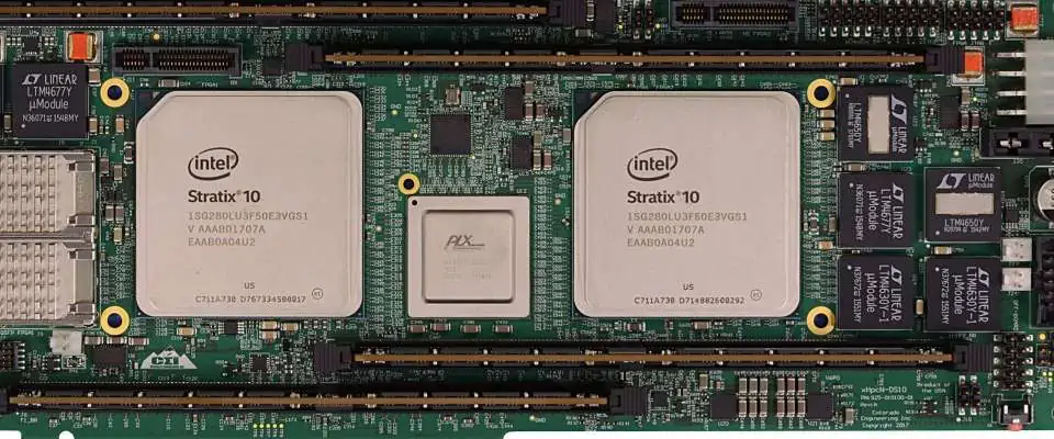
A typical FPGA contains a set of memory and control registers. It can also store and process data. Intel, for example, has an FPGA with a memory interface that supports up to 57.8 Gbps. The Stratix 10 GX FPGA has PCIe Gen3 x16 and a 10/25/100G Ethernet MAC. These devices are useful in high-bandwidth performance applications.

Intel Edge-Centric FPGAs

If you are in the market for an FPGA chip, you may have noticed a new type of device in the market called Edge-Centric FPGAs. This type of chip combines a hardware processor and a software-defined peripheral. Intel Edge-Centric FPGAs are ideal for small form factor, low power applications. These chips provide the flexibility and longevity required for low-power applications with an instant-on capability and on-chip flash memory.

Previously, Intel insisted that its Xeon processor handle nearly every computing task without the help of an FPGA. However, Intel has taken a different approach and created a new platform that incorporates FPGAs with next-generation memory and custom chips. The result is a platform we call AgileX. As a result, edge-Centric FPGAs are capable of delivering high-performance compute to mobile devices.

For applications that require high-bandwidth performance, Intel offers an Edge-Centric FPGA called Cyclone 10 GX. The Cyclone 10 GX FPGA delivers up to 12.5 Gbps of transceivers. In addition, the Cyclone 10 GX FPGA comes with both a soft-core processor and a dual-core ARM A9 hard processor.

The new processors from Intel are targeting the next generation of servers and network equipment. Swan, former Intel’s CEO, had explained that the company is moving from being PC-centric to being data-centric. With the cloud data center becoming increasingly centralized, Intel is focusing on a data-centric product portfolio to combat Moore’s Law slowdown. This is a step in the right direction for Intel, which is trying to position itself as a leading chip provider for 5G networks.

Next-Generation Intel FPGA Video Test Chip

With its 224 Gbps-PAM4-LV transceiver test chip, Intel has taken a significant step forward in the FPGA industry. The new chips offer flexibility, scalability, and outstanding power and performance for bandwidth-intensive applications. Here are some of the key benefits of the new chip:

The 224 Gbps-PAM4-LSR Transceiver features a high-speed I/O and a PAM4 modulation scheme that reduces noise and jitter. These features are key in video applications. In addition, the chips’ low-power designs are in a way to minimize energy consumption. As a result, they are useful for any application where the high-speed video is required.

With a base 10nm design, the new chips feature an ecosystem of chiplets. In addition to enhancing the FPGA’s fabric, Intel offers a range of new features, such as a hardened bfloat16 AI data type, dedicated AI acceleration, and 116G transceivers. They also support PCIe 5.0/CXL and DDR5.

The next generation FPGA is future-proof and uses a chiplet approach. For example, to enable PCIe 5.0, Intel would have to design a new chiplet to support it. And Xilinx would have to develop a monolithic chip to get it. In contrast, Altera’s chiplets will integrate Arm cores and HBM with the FPGA, allowing it to improve time to market and performance.

Another major benefit of these devices is the ability to create highly custom-designed solutions. Using the power and flexibility of FPGAs, Intel is creating an entirely new platform to accelerate the development of advanced applications. Moreover, its software-defined capabilities can leverage its vast ecosystem and partners for a broad range of applications, including high-end video applications.

Design and Development With Intel FPGA

If you want to design and develop circuits for Intel FPGA, you must have an Intel Quartus Prime design software. This software comes in three different versions: Pro Edition, Standard Edition, and Lite Edition. The Pro Edition requires a paid license while the Standard Edition is free. For the Lite Edition, you can download the software for free. In addition, Intel’s Integrated Circuit Design (ICD) software enables you to model digital signal processing algorithms.

The software environment for designing and developing with Intel FPGA has many benefits. For example, designers can generate a high-level design in Simulink and refine it for implementation using FPGA and SoC hardware. During this phase, they can apply optimizations to increase performance and lower FPGA resource usage. Moreover, the hardware cosimulation allows them to verify if their designs actually work on the FPGA.

The Intel FPGA Tutorials describe various design flows. They are meant for laboratories and should be followed accordingly. They also contain version numbers, which correspond to Intel Quartus Prime software versions. With these tutorials, you can design and implement logic circuits for Intel FPGA devices. These tutorials provide a guide on the fundamentals of logic circuits and the design process. They also have sample designs for you to emulate and simulate.

The software and hardware integration of these devices allows for efficient communication between different devices. The MAX 10 FPGAs come with features like analog-to-digital converters and dual-image flash. They also come with SRAM-based configuration cells. They are also capable of supporting the Nios II soft core embedded processor. Despite their small size, they have lots of capabilities. Aside from the software-intensive features, the MAX 10 FPGAs also have GPIO and DSP blocks.

Conclusion

Intel FPGA is one of these innovations that every company would have wanted in their own product development process. It is an innovation that could have a huge impact on the computing world. Intel is one of the top companies that provide machinery for other companies to build on and has a way to implement their technology into other things.

What are the Major Foundational Areas and Challenges of Supply Chain Management in Electronics Industry?

Supply Chain Management

As the manufacturing companies of today face serious global competition, they now seriously seek innovative strategies to help them stand out. This is why supply chain management is important, because it is one of the important strategies. A supply chain system that is properly designed helps in improving product quality, boost efficiency, and enhance customer satisfaction.

What is Supply Chain Management?

The traditional acquisition of commercial innovations in processes and services were first achieved by companies with vertical integration. Later, this global competitive industry took on a vertical integration structure that permitted interaction between manufacturers, suppliers, and clients.

Furthermore, supply chain management has to do with an interconnected network of corporations in either service delivery on product manufacturing. Also, supply chain also serves the distribution logistics and manufacturing chains. Manufacturing logistics chain deals with the business processes that are linked onto production. The distribution logistics chain on the other hand deals with the after-sales and involved operations, which includes the maintenance and repair of products.

As a result of global economies from globalization, there is now more attention on the supply chain. You can refer to manufacturing as an activity offering more value to a specific material. Due to the fact that each step plays an important role in the process, let us consider the main the major foundational areas of supply chain management in electronics manufacturing process.

Major foundational areas of supply chain management

Supply Chain

This supply chain is regarded as an integrated system, which enables members of organizations to help in addressing and collaborating the concerns of material and information flow. This integration model was created to analyze multi-product complexities, check out and address different planning strategies to provide answers to multi-period problems and issues, as well as capture whatever technology has been used. This integration model helps in integrating sourcing decisions, production, and distribution.

Here, information usually flows upstream, in contrast to materials that flow downstream. This means information travels down from customers, to logistics, suppliers, and manufacturers. Later, the supply chain will come into the picture streamlining the communication and also causing its simultaneous flow. This allows electronic manufacturing process activities to achieve coordination both upstream and downstream.

Transportation

How transportation techniques progresses defines the servicesโ€™ efficiency. Management principles that are well-devised help in enhancing operation costs for delivery speed, energy-saving, quality of service, and moving load. Due to nationalism and globalization in the last decades, logistics management has now become critical and important to quick and on-time delivery.

With logistics, you will be able to optimize the existing manufacturing processes as well as distribution when promoting the efficiency and competitiveness of a specific company. The transportation system is one very important element. A robust system is made of a good transport implementation and clear logistics for continuous supply chain operations.

Warehousing

This is a very important aspect in supply chain. As of today, there are obvious changes in supply chain, technology, and environmental sustainability. All these affect warehousing. This is also called distribution centers and warehouses do not really add value to supply chain of products that are bought in bulk or large quantities.

Also, they can be more efficient compared to the other products. This efficiency comes in when the products you have designed to be shipped are consolidated. This cuts transportation costs. It also completes other different value-added tasks, which include branding, packaging, labeling, etc.

Sourcing

The huge competition in the industry as well as how raw materials have fluctuated has led to the increase in the need for better management of suppliers. There is more emphasis on managing suppliers offering materials that are required to satisfy a customer demand.

Teams involved in procurement and sourcing are usually focused on balancing both the external and internal demands of the customers. Also, it considers the role of supply distribution and technological change.

Returns Management

This is a process whereby activities that are linked to reverse logistics, gatekeeping, and returns are managed in the organization. When you implement properly, you allow the administration to take charge of the reverse flow of the product efficiency, as well as reduce or lessen unwanted returns.

Note that failure to consider the reverse flow can lead to some missed opportunities. This means that effective management of returns could affect your financesโ€™ performance positively. It will also assist you in building a stronger relationship with your customers.

Post sales services

These have some strategic relevance with a firm. They have the potential ability to boost customer retention, product development, and profitability. Consumers purchase products when there is a need to find answers to some problems.

 Sadly, majority of managers fail to realize that products that are electronically manufactured and purchased should service the customers or end users. Supply chain management is majorly concerned with the managing reflows. The post-sales service works with different supply chain managers present in operational, relationship management, IT, finance, and forecasting processes.

Collaboration and Partnerships

Collaboration and partnership is the major force involved in supply chain management. Though, all these are not completely leveraged, there is a need for companies to realize that these supply chain partners seek to form a partnership to ensure mutual benefits.

Partnerships and collaboration makes the difference between long โ€“term sustainability and profitability and short-run dissolution. The benefits here have surpassed efficiency and effectiveness to enable companies to help meet customer demands, increase market share, and grow markets.

The seven foundational aspects of supply chain management should assist different companies in handling the realities of the next huge opportunity, coupled with meeting customer needs. The goal has to be to have customer loyalty, maintain quality, and increase efficiency.

What are the Challenges of Electronics Supply Chain Management?

Back in 2019 and before then, the discussion relating to the supply chain usually revolved around counterfeiting, component shortage, and electronic products lifecycles. Due to COVID-19 as well as the second wave sweeping the world, these issues seem easy when compared to widespread shortages, factory closures, as well as all-around uncertainty. Though there has been a shift in attention, the earlier challenges of supply chain will have to be checked after our modern life returns to normal.

Major Challenges in Electronics Supply Chain Management

The landscape for electronics sourcing was in chaos and it is likely to continue like this. Global supply chain was specifically designed for buyers to detect the ideal trade-off between minimum lead time and the lowest price possible. This means that buyers might tolerate higher prices if electronics suppliers can meet the production schedule. Also, this involves electronics manufacturing in higher volume. Therefore, customers might accept a longer lead time.

Buyers have the free will to choose their sources. Therefore, they can take advantage of the logistics system despite tariffs and shortages. There are some challenges in the electronics supply chain management. EMS companies are trying all means to overcome these challenges.  Below are some of the challenges faced in the electronics industry:

  • Shortages are still a major problem for fundamental parts designed with legacy technologies.
  • The electronics industry performed well compared to some industries
  • Electronic buyers now focus on the possibility of new shutdown and restricted activity
  • There was erratic demand in the component industry and this resulted in erratic supply. However, the industry was experiencing growth.
  • OEMs and EMS companies now experience shortages and long component lead time.

All of these challenges will result in three crucial electronics supply chain management problems faced by the electronics industry:

Shorter product lifecycles

Shorter product lifecycles are a result of more rapid development in technology. Also, changes in consumer behavior contributed to this problem. Therefore, these create inventory management problems. Also, companies now need extra inventory to meet the demands of customers. Companies have to turnover inventory more. Therefore, this increases the risks and cost of carrying inventory, especially if a product experience failure.

Also, depending on a centralized manufacturing base makes it hard for companies to get the components they require. This is more difficult when there are global supply chain disruptions.

Lack of diversity

There are several primary and secondary electronics distributors across the world. Some of these distributors have maintained relationships with major component producers. However, they are fewer major electronics manufacturers for components. This lack of production diversity has become obvious due to geopolitical chaos in the form of tariffs.

Also, the just-in-time supply chain model depends on predictability. This model has been so slow to adjust to sudden shocks.

Product complexity and commoditization

This explains the reason behind shorter product lifecycles. Shorter product lifecycles exist because each portion of the design chain and supply chain is now commoditized. Therefore, companies keep introducing more complex and newer electronic devices just to remain competitive. While, this is good for the end customer consumer, it isnโ€™t beneficial to electronics companies. This may drive competition and reduce prices for consumers. Also, it helps consumer to enjoy all the features in the products.

However, this situation has made OEMs to outsource almost everything except the IP. This will only remain that way as long as there are regulations that donโ€™t prevent this. Also, this factor has contributed to Chinaโ€™s rise as a manufacturing center in Asia.

There are several ways to address all these challenges. One of such ways is to minimize the risk and diversify electronics supply chain in Asia. Also, the electronic supply chain industry should focus on other countries in Asia.

More Diversified Supply Chains

Globalization has impacted the world in several ways. It is great for consumers in advanced countries. Also, it has increased wages and improved livelihood in poorer countries. However, we still need to address the ethical questions around environmental damages and working conditions. Also, differences in labor cost in China and other countries are beginning to close.

The current global chaos is now forcing EMS and OEMs companies to have a rethink on the competitive advantage of wage differential. There is an increased risk with lower labor costs. This can be unacceptable for crucial components.

Furthermore, the gradual increase of labor costs made the industry to have a rethink using China as the manufacturing powerhouse in the world. The discussion focused on developing regional production and distribution centers. This will help eliminate China as the only source for several components and cheap assembly services.

However, people might not see this effort as being worth the capital and time investments since no one like to remember Black Swan events. Also, the whole network of distributors is still in Chinese hubs. The failure of just-in-time logistics has created motivation for the regionalization of production and distribution capacity.

 OEMs and system integrators can diversify their supply chain away from Asia and make supply chain closer to home. There will be some benefits if electronics manufacturing services man can achieve this.

Benefits of Diversifying Supply Chains

With chinaโ€™s existing supply of consumer electronics and other electronics products, the supply chain visibility is low. There is a need for new markets. Diversifying supply chains will help to meet more consumer needs.

Traceability

There are fewer opportunities for any form of counterfeiting if components get to fewer hands. Also, this makes raw materials and components much easier to trace in the electronics industry.

Less risk

More sources result in less risk. Spreading production capacity across a broad geographic region will minimize the risk of regional disruptions like tariffs. Also, this offers a competitive advantage for consumer products.

Easier to protect IP

This will reduce any risk of IP theft when different parts of a new productโ€™s assembly are widely spread to various regions. Also, IP theft may be easier to trace if there is more localized supply.

Conclusion

The United States is moving in this direction. Some years back, there was less focus on onshoring. The Trump administration began to push an initiative to onshore industrial supply chains. Therefore, this will reduce the dependence on China.

When high demand results in limited available production capacity for a particular product, it is crucial to create priorities. However, we might likely see how the proposed trace policies by Bidenโ€™s administration will impact dynamic onshoring. Also, the EU is trying to achieve this same goal, especially for the pharmaceutical industry.

This is a complex challenge that is worth undertaking. With the shifting manufacturing capacity and disruptions in the supply chain, there has to be breakthrough. Presently, Southeast Asia still remains the manufacturing Hub. However, with new implementations taken into place, change can take place.

How to Design Your Own Circuit Board

PCB design

The design and board layout can be regarded as a science and an art. To start with a circuit board design from the scratch could be difficult. If this is your first time working with printed circuit board and electronics design, and you still have something to learn regarding custom pcb design, we have compiled some important steps to help you achieve this.

So much is involved in the engineering of a printed circuit board (PCB) design, from the basic type of printed circuits to a non rigid and complex PCB. New electronic devices will begin as block diagrams and some electronic schematics. Immediately you have completed and validated the schematics, then you can follow these steps in creating the PCB layouts of today.

What does a Circuit Board Mean?

Printed circuit boards (PCBs) offer some mechanical support and connect the different electronic components making use of pads, conductive tracks, as well as other features that are etched from the copper sheets, and then laminated to a non-conductive substrate. In addition, printed circuit boards come with copper traces or copper layers that are pre-designed on the conducting sheet.

These predefined tracks help in reducing the wiring, therefore reducing faults that can arise as a result of loose connections. All you need to do is place those surface mount components on the printed circuit board (PCB) and then solder them.

Our article will reveal and teach you how to make your own circuit boards prototype from the comfort of your home. When you do this, you will save yourself a lot of time from double checking and debugging the connections to a breadboard. Furthermore, after this tutorial, you can go ahead and make your Arduino. Therefore, get ready and learn how to do it!

Ways of Making Your Circuit Board

Three main methods are useful when making a PCB. These include

  • Circuit by hand method
  • Iron on Glossy method
  • Laser method

Since the last method โ€“ laser method โ€“ is well-known as the industrial way of PCB manufacturing, we will have to learn more about the other two methods. For the sake of this article, we will be learning how to make circuit boards using Altium designer.

PCB Design is achieved by the conversion of the schematic diagram of your circuit into the PCB layout making use of a pcb design software. A lot of open source softwares is available for PCB design and layout creation. Some of them include PCBWizard and Autodesk Eagle.

Here is a complete list of the steps involved in the PCB board design and PCB layout.

  • Creating the schematic diagram
  • Creating the blank PCB layout
  • Capturing the schematic โ€“ linking it to your printed circuit board
  • Designing the PCB stackup
  • Define the DFM requirements and design rules
  • Place the components
  • Insert the drill holes
  • Route the traces
  • Add identifiers and labels
  • Generate the design files

Now, letโ€™s understand these steps one after the other.

Schematic Capture

If you are generating the pcb design of your printed circuit board from a specific template or you are creating the PCB from scratch, the best thing to start with is the schematic. This is similar to the new deviceโ€™s blueprints. Also, understanding whatever is shown in the schematics is also very important. First of all, the schematics have to include the following:

  • The components used for the printed circuit board design
  • The way these components are linked or connected
  • The relationships formed between these components in the different schematics

This last point is very important. This is because complex designs can make use of hierarchical schematics. Furthermore, you can make sure that there is a serious organization in the new board if you make use of hierarchical approaches into the printed circuit board design and then go ahead to place these circuit boards in the different schematics.

Creating the Blank PCB Layout

After creating the schematic, you will need to use a tool in the Altium designer to help in importuning the components into your blank PCB layout. The first thing to do, is to create a blank document for your PCB which generates a PcbDoc file.

If the layer stackup, dimensions, and shape of the PCB (printed circuit board) has been predetermined, then it is time to set them. Also, if you donโ€™t wish to perform the tasks at that moment, do not fret; the layer stackup, size, and board shape can easily be changed.

The compilation process deals with the verification of the pcb design as well as the generation of different project documents. This allows the inspection and correction of the pcb design before transferring it to the PcbDoc. Also, it is very necessary that you check and update your Project Options. These are useful in the creation of the information for the PcbDoc.

Capturing the Schematic โ€“ Linking it to Your Printed Circuit Board

The tools in the Altium designer usually work in a pcb design environment that is united, whereby the BOM, PCB layout and schematic are interlinked. Also, you can access them simultaneously. There are other programs which aid the manual compilation of the schematic data.

However, this Altium designer helps you achieve this automatically as you engage in your own printed circuit board design creation. To transfer your SchDoc information onto the PcbDoc you just created, click Design and then update PCB. A dialog opens โ€“ Engineering Change Order, which opens and lists all the nets and components from the schematic.

Designing the PCB Stackup

After transferring the schematic information onto the PcbDoc, then the footprints of the components will be revealed. This also includes the specification of the board outline. Before you place the components, make sure the PCB layout is defined. This includes the layer stackup and shape, making use of the Layer Stackup Manager.

If this is your first time doing PCB design, the majority of modern concepts for PCB board design begins with 4 layer boards on FR4, though it is possible to define your specific number of layer on the Altium designer.

If you are dealing with high frequency/high speed circuit board design, then you can make use of the in-built impedance profiler. This is to make sure that there is impedance control in the board.

Define the DFM Requirements and Design Rules

The number of categories for the circuit board design rule is extensive. You may not have to make use of the available rules for all designs. You may deselect/select the individual PCB rules just by tapping and right clicking the rule from the list. The printed circuit board design rules can be categorized into the following:

  • Clearances in-between objects present in the PCB layout like between pads and traces
  • Solder mask or copper traces feature the size limits like solder mask silvers and holes
  • Routing rules, which includes length limitations and trace width, which can be enforced on some nets
  • Signal integrity and high speed limits like overshoot
  • Clearances and limits of board fabrication like board edge clearance

Place the Components

 The Altium designer offers great flexibility. It also allows the quick placing of the components on the circuit board. With this, it is possible to arrange the components automatically or place them in a manual way. Make sure you take advantage of the auto-placement speed to make sure the laying out of the circuit board works with good guidelines for component placement.

Insert the Drill Holes

Before you route the traces, it is advisable to place the drill holes. This includes the vias and mounting. If there is a complication on the circuit board design, then it is necessary to modify some via locations when trace routing is ongoing.

Route the Traces

Immediately the components have been placed as well as other different mechanical elements, then it is time to route the traces. While you route the circuit board, try to come up with a unique strategy that helps in first finishing the important routes properly. Next, fill the gaps using the connections remaining as required.

Some important routes include power nets, noise-sensitive nets such as low-level analog signals, and other impedance-controlled nets. Ensure to make use of good guidelines for routing. Also take advantage of the altium designer tools to help in simplifying the process.

Add Identifiers and Labels

After verifying your circuit board layout, then you are set to add markings, identifiers, logos, labels, as well as other imagery on printed circuit boards. Including the reference designators for the components is a great idea as this goes a long way in the PCB board assembly.

Furthermore, ensure that the pin 1 indicators, polarity indicators are kept visible because they aid PCB testing and PCB assembly.

Generate the PCB Design Files

 Before creating the manufacturer deliverables, it is a great idea to verify the layout of the circuit board by conducting a DRC โ€“ design rule check. This can be done automatically with the Altium designer as you route the circuit board design and its components. However, it isnโ€™t a bad idea when you conduct a manual DRC. Once the printed circuit board has successfully passed the last DRC, then thereโ€™s a need to get the design files.

Conclusion

By now, you should know how to design your own circuit board. If you have any questions, please reach out to us here.

How to Clean Circuit Board Corrosion

Clean Circuit Board Corrosion

Corrosion is a major enemy of printed circuit boards. Circuit boards that are sufficiently corroded cannot work. Furthermore, be sure that the steady advancement of corrosion must happen. However, the question now is why printed circuit boards corrode. You may also be wondering what causes PCB corrosion.

In this article, we will explain what PCB corrosion is, the types, and the ways of getting rid of them, and measures you should take to prevent them. Please read on as we give more explanation concerning the topic.

What Does PCB Corrosion Mean?

Anytime, oxygen forms a bond with any metal surface, oxidation takes place. This could lead to rust and add to flakes of metal surfaces that break away. Due to the fact that pcb pads and pcb traces are manufactured from metals like copper, there is always a risk of corrosion.

Note that different metals corrode at different rates. There are metals that corrode immediately they get some exposure to oxygen, while some others may not even corrode in any way. High corrosion metals include silver, gold, copper-metal alloy, and graphite.

Also, metals that will most likely suffer from serious or severe corrosion include copper, lead, plated nickel, and plated tin.

What Causes PCB Corrosion?

Corrosion could be caused by different things, which includes capacitors, leaking batteries, weather damage and water damage. No matter the quality of corrosion on the circuit board, it could cause it not to function or work properly. Furthermore, it may even cause the components to experience more damage. Over time, corrosion can become worse and in the end can cause or lead to irreversible damage.

What are the Forms and Types of Corrosion?

 corrosion on pcb

With respect to the root of the parts rusting, the different forms of corrosion include

  • General attack corrosion
  • Galvanic corrosion
  • Localized corrosion
  • Intergranular corrosion
  • Electrolytic dendrite corrosion
  • Fretting corrosion
  • De-alloying corrosion
  • High-temperature corrosion
  • Environmental cracking corrosion
  • Flow-accelerated corrosion

The general attack type is the most significant form and it works on bigger surfaces. For localized corrosion, it affects just a small portion. In addition, galvanic corrosion takes place when two metals start corroding as a result of corrosive electrolytes.

The metal present in PCBs (printed circuit boards) can experience corrosion in different ways. These include:

Galvanic

This galvanic corrosion occurs or takes place when different metals come in contact with an electrolyte. When galvanic corrosion occurs, metals that are more resistant will corrode much faster compared to the baser metal that it forms a contact with. Therefore, whenever tin comes in contact with gold, for instance, the gold corrodes faster than expected.

Atmospheric

This corrosion type is known as the most standard. Here, metal gets exposure to moisture containing oxygen. This causes a reaction whereby there is a bond formed between the oxygen atoms and the metal atoms, creating an oxide.

It is very easy and ensures that copper experiences atmospheric corrosion. This isnโ€™t an issue for copper plumbing. This is due to the fact that corroded copper retains or hold on to its mechanical properties. However, it fails to keep its electrical conductivity, thereby making circuit boards have a huge problem.

Fretting

When there is fretting corrosion, when the solder-plated switches close, it creates some wiping action, which helps in the removal of the surface oxide layer. This allows or makes it possible for the layer underneath to oxidize. This then leads to excessive rust building up and preventing the activation of the switch.

Electrolyte

For this metal degradation, the adjacent traces see a dendrite growth anytime the electrical voltage formed between them is infected by contaminated moisture. This creates metal slivers that cause short circuits.

Ways of Cleaning Corrosion from Circuit Boards

If the printed circuit board gets some corrosion as a result of water damage or through a different source, then you may repair it just by cleaning it.

To clean a circuit board, you will need daily household items which any company can afford. The issue here is that only individuals having the necessary knowledge of PCB electronics should make attempts to clean a PCB.

This process deals with the disassembling of the board and making sure that no damage comes to the components. Furthermore, when the PCB is separated from the electronics, keep a distance from the water and then disconnect your device.

To clean a printed circuit board (PCB), you can use a whole lot of different cleaning tools. However, some items function well for getting rid of corrosion. These materials are useful for cleaning or to clean a circuit board corrosion.

What are the Materials Useful for Cleaning Circuit Board Corrosion?

Distilled water

With the use of water for cleaning or to clean a circuit board, ensure that there are no contaminants in it. The ions that are present in the regular water feature conductive properties, which degrade electronics. However, distilled water features no ions or contaminants, which can lead to damage.

Baking Soda

Note that the abrasive and alkalinity qualities of the baking soda ensure it is a perfect choice for all corroded printed circuit boards (PCBs). Baking soda helps in clearing and neutralizing corroded areas preventing damage.

Soft-bristle thin brush

If there is no specialized PCB cleaning tool for your PCB (printed circuit board), you can make use of a paintbrush or toothbrush. This also works. Brushes having soft bristles will prevent a scratch coming to the delicate components of the board.

Household cleaner

Household cleaners that are phosphate free can effectively get rid of corrosion and dirt. Phosphates offer some protection for PCBs (printed circuit boards) from corroding. However, they can cause water pollution.

Compressed Air

Now, compressed air is a method that is non-disruptive in clearing accumulated dust within electronics and on surfaces. This method helps in blowing air into the gadget via the deviceโ€™s open spaces. Furthermore, if there are small spaces, be careful when opening the equipment and then clean the circuit board carefully using the compressed air.

 Oven

Using your usual household oven helps in drying a printed circuit board thoroughly when using indirect heat. Make sure that you switch off the oven first, before you place the circuit board inside it.

Lint-free Towel

Clothes that are manufactured from microfiber as well as other fabrics that are lint-free, aid the speed up of the process of drying without leaving out any particles.

How to Use Baking Soda for Cleaning Printed Circuit Boards (PCBs)

These materials above help in restoring the PCBโ€™s corroded areas. Work with these steps and use baking soda importantly so as to clean corrosion from your circuit boards.

Record the configuration and layout of the PCB. Make sure you capture all the details with pictures or notes. This will help you when reassembling the board after you are done cleaning it.

Remove or disassemble the chips and cables of the PCB. With this step, you will be able to access all the corroded parts of the circuit board.

Clean making use of distilled water and baking soda. Combine a part of the baking soda with about 2-4 parts of water till it turns into a thick paste. Next, make use of the brush in scrubbing the cleaning solution in all the corroded areas. Next, allow the circuit board to dry for about 20 โ€“ 30 minutes. You can then use additional distilled water for rinsing.

Make use of household cleaner to do another pass. Ensure that you use the cleaner to spray all the corroded parts. After this, make use of a clean brush for your scrubbing once again. Lastly, make use of your lint-free towel in patting the circuit board dry.

Use your oven to dry your PCB. Set it at 170 degrees and once it has completed the preheating, turn it off properly. Next, place your circuit board into the oven and allow the heat to dry the remaining moisture.

Get the board reassembled and tested. Place the components together and then check the functions of the PCB once again. Make use of an eraser to remove the leftover corrosion if you discover that the circuit board is still not working.

What are the Effective Methods for Removing PCB Corrosion?

Two ways exist for cleaning corroded circuit boards. These include making use of a solution that has been mixed with baking soda, alcohol, and water. The other is making use of a special cleaning spray for circuit boards.

Below are some other methods.

Always make sure that you first of all remove the power source and batteries of the device. This prevents short circuits. It also prevents possible injuries. Note that when doing this, you may expose some other elements of your device to corrosion. Therefore, make sure that you do this very carefully.

You can easily find corrosion when you see a greenish or white substance looking and feeling crusty. The common places you should check are battery connectors, charging ports, connectors for SIM cards, as well as other mechanisms that will permit the connection of wired accessories onto the device.

Make use of Q-Tips or cotton swaps. You can also use water, baking soda, and isopropyl alcohol to clean up the corrosion. Vinegar is also useful. Apply this mixed solution onto that affected area. You can then wipe it back & forth to ensure that the corrosion disappears. This solution can also be applied onto the corroded part and then allowed to sit for long periods before you wipe it off.

Make use of the soft cloth or cool setting of a hair dryer to dry up the device. Never make use of heat to achieve this. Before you get the device back on or replace the batteries, ensure that you have dried the circuit board completely

 Replace any damaged battery with a new one. Also, ensure you recycle the old one properly. Donโ€™t dispose of them with any trash. This is because it can cause damage to your environment.

Ways of Preventing Corrosion on a PCB

Now, the question is, what ways can you prevent corrosion from coming to the PCB? You cannot avoid corrosion for forever, however delaying it is possible beyond the circuit boardโ€™s expected life. However, what are the steps necessary to achieve this?

The major goal when you are preventing PCB corrosion must be to prevent ionic contamination. When you expose components of circuit board to moisture, the ionic contamination is known as the major cause of corrosion in printed circuit boards. The first ever priority has to be to ensure that the pcbs as well as its components stay dry and clean.

Also, it is very important that this priority is kept in mind during the manufacturing of PCBs. Fabricators have to avoid getting liquids and fingerprinted on the printed circuit board and ensure that the boards are manufactured in a dry and clean environment. Also, designers have to take care and prevent moisture from beading up on the exposed conductors.

Also, when designing printed circuit boards to be used in applications that will most likely expose them to more liquid contaminants like industrial environments, agricultural industry, and automotive industry, you have to take some important steps in protecting your circuit boards from any environmental hazards that will likely happen.

Ensuring that the PCBs are kept dry and clean enough to prevent or ward off corrosion is easy. You only need little attention and care. However, taking any of these preventive steps doesnโ€™t mean that corrosion will come to your PCBs. But the fact is that this reduces the possibility of corrosion happening and it is worth the care and effort.

Conclusion

You can learn more about ways by which you can prevent corrosion from coming to your printed circuit boards. For some reliable information to learn how Rayming PCB & Assembly ensures that their printed circuit boards resists corrosion, or you wish to learn other strict quality assurance methods we adhere to, please contact Rayming PCB today.

The Manufacturing Process of Stencil Electronics

Stencil Electronics

Stencils are important in electronic manufacturing. These days, electronic manufacturers use stencils to print solder paste. The paste creates deposits on the printed circuit board to firmly hold electronic components. It is important to apply the paste in the right volume and position. This precision is very important when applying paste.

Therefore, the use of stencils is crucial in applying solder paste. These stencils help to regulate solder paste printing. Also, stencils make solder paste application easier for surface mount device (SMD). Stencils offer great benefits to electronics manufacturing. In this article, we will discuss the role of stencils in electronics manufacturing.

What is PCB Stencil?

A stencil is a sheet of steel used to apply solder paste on a circuit board for SMT component placement. Also, the PCB stencil features laser-cut openings. This stencil deposits the paste on marked areas on a bare circuit board. Therefore, it keeps components placed on the circuit board firm.

The main function of a PCB stencil is to deposit the appropriate amount of paste on SMT pads.  This enables the solder joint between the component and the pad perfect as regards mechanicals strength and electrical connection. A PCB stencil makes the application of paste easier and faster. Also, it ensures accuracy and precision when applying paste.

PCB stencil manufacturers design stencils by creating holes via lasers on a stainless steel foil. These holes are created at the positions where PCB assemblers need to place surface mount components on the PCB. This allows the PCB assembler to place the stencil on top of the circuit board and align it using position points. These positioning points are also known as fiducial marks.

After proper alignment, the assembler applies the paste using a metal squeegee blade. Therefore, the paste is generously and precisely applied to the bare circuit board. After this, the assembler can place the components on the circuit board.

A PCB stencil manufacturer creates apertures or openings through laser beams on a hard steel-foil based sheet. The stencil is then placed on top of the circuit board. Solder paste stencils, reusable stencil frames are permanently glued. The metal stencil and lead free solder paste. Laser cut stencil are the best option for PCBs. Electroformed stencils offer good quality.

Important Considerations for PCB Stencil Design

Stencil thickness

The thickness of the sheet determines the amount of solder paste released through the opening. With the accurate thickness, the PCB stencil will release the desired amount of solder paste.  The aperture size and the sheet thickness are crucial factors that impact the amount of solder paste deposited on the PCB.

Also, deposition of extra solder can result in solder bridging. Meanwhile, deposition of less solder can cause weak solder joints. Therefore, this can affect the performance of the final printed circuit boards.

Aperture design

Another crucial factor that can affect solder joint is the aperture design. The chances of defects like solder beads and solder bridging depend on the aperture design. The opening of the stencil is usually smaller than the pad size of the circuit board. It is possible for the solder paste to stick to the aperture wall after solder deposition. Therefore, the PCB padโ€™s area should be more than two-thirds of the area inside the aperture wall.

Stencil alignment

Stencil designers add registration marks known as fiducial marks to the stencil and PCB. These marks help to ensure proper alignment between the stencil and PCB.  Also, it helps to achieve a perfect print of solder paste.

Stencil material

The material of the stencil will impact its ability to provide paste from the aperture to the PCB pad. The best material for stencil is stainless steel. This is a major reason why stainless steel stencils are commonly used in the PCB industry. Also, the stencil material determines solder paste release via the apertures.

Types of PCB Stencils

There are different types of PCB stencils.

Framed PCB stencils

These stencils have a casing around them. The stencil frame ensures the stencil sheet is tight enough for the appropriate exactness.  Also, framed stencils are specifically designed for a high degree of screen printing of PCBs. Framed stencils feature smooth aperture walls. Also, these stencils have clean laser-cut apertures. Therefore, it creates permanent non-fading fiducial.

Frameless stencils

Frameless stencils are laser cut solder paste stencils. These stencils work with stencil tensioning systems. Frameless  SMT stencils are less expensive than framed stencils. Also, they deliver great quality and performance despite their low cost.  These stencils donโ€™t feature a fixed casing around then.

Prototype stencils

Prototype stencils are usually made from Gerber or CAD files to match prototype printed circuit boards. Also, these stencils are frameless. Prototype stencils are specially designed for manual printing.

Electroformed stencils

These solder paste stencils are usually nickel-based. An electroformed stencil provides the best release of solder paste.  Also, these stencils are widely used for fine pitch. The nickel in electroformed stencils feature a low coefficient of friction compared to that of stainless steel. Also, electroform foils are much harder than hard stainless steel. This offers a longer stencil life.

How to Manufacture A PCB Stencil

A PCB stencil feature hundreds or thousands of opening created with high precision. Therefore, it is not advisable to manually create these holes. There are three methods for making circuit board stencils. These methods are electroforming, chemical etching, and laser cutting. The laser cut stencils is the most popular PCB stencil.

Here, we will go through the process of PCB stencil manufacturing by using a laser cutter.

Stack the mylar sheet

You need to stack two sheets together. Then, heat the mylar sheets until you detach the first sheet from the stack.  The second sheet will suck the melted pad of the first sheet. Therefore, this allows you to pull the first sheet off.

Export design files from EagleCAD

Export your cream layers via a cam file. Using ExpressPCB, open the file menu and choose the โ€œExport DXF Mechanical Drawing.โ€

Swell pads in viewmate

You will have to compensate for the melting caused by the cutting process. This is because meting enlarges the pad size. Therefore, you will have to cut down the size of the pad. To import the cream layers into ViewMate, you need to choose File>Import>Gerber. After this, select Setup>D codes. Choose all columns and open Operations>Swell. Input the value for the size adjustments based on the laser specifications.

Use Autocad to swell pads

You can use AutoCAD to scale down the DXFโ€™s content. Also, you will need to highlight the drawings in the AutoCAD window. Key in the proper scale figure when the Scale Factor dialog comes up. This will place the drawing in the appropriate scales. After doing this, you can now print out the finished drawing.

Cut the stencils

You will need to adjust the settings on the laser cutter to appropriately cut through the already stacked Mylar sheets. The laserโ€™s heat will melt the first sheet. However, the second sheet will absorb the first sheetโ€™s melted pad. Therefore, this enables you to neatly pull out the first sheet.

How to Ensure Quality Solder Paste Printing

PCB assembly involves solder paste printing. Therefore, precise printing of this paste is crucial for accuracy for a PCB assembly. However, some crucial elements help to ensure quality paste printing.

Stencil installation

Pool alignment of stencil can result in solder bridge. Therefore, it is crucial to ensure there is precise alignment between the circuit board and the stencil.

Blade stroke speed

Blade stroke speed will impact the amount and shape of the paste deposition. Also,this affects the solder paste printing quality. Generally, you should set the stroke speed between 20 to 80mm/s. You must adjust the bladeโ€™s speed relative to the solder pasteโ€™s viscosity.

PCB mounting

Before you start solder paste printing, you need to mount the target PCB to the work table using a vacuum or mechanical clamp. Also, you should secure this circuit board with support pins at the center of the circuit board. This ensures it doesnโ€™t move during printing.

Squeegee pressure

The pressure of the squeegee blade will impact the amount of paste deposited. If the pressure is more, there will be less solder deposition. Also, this is because the pressure squeezes the gap between the circuit board and the stencil.

Squeegee blade set up

After mounting the stencil firmly on the printed circuit board, you will apply the solder paste to the stencil. You will need a squeegee blade to fill paste in the stencil apertures.

Thorough cleaning

Thoroughly cleaning the stencil will get rid of any solder paste. Also, this will get the stencil prepared for the next printing.

The Importance of Stencil in Surface Mount Assembly Process

Stencil is widely used in the surface mount assembly process to achieve an accurate and repeatable deposition of solder paste. High volume screen printing can impact PCB board functionality. Also,the stencil design is crucial to achieving a high-yield assembly process.  Low amounts of solder can cause dry solder joints.

The type of surface mount devices on the PCB determines the optimum foil thickness.  The thickness of the stainless steel foil varies. Also, laser-cut stencils are commonly used for surface mount device.

Conclusion

Stencil printing is an integral aspect of PCB assembly. Also, this process could be very tricky. The slightest error can ruin the whole PCB assembly process. Also, PCB stenciling helps to mount all solder joints in the PCB. This helps to save time and eliminate error in the solder joint. The PCB stencil helps to achieve smooth aperture walls. Printed circuit boards perform better with accurate stencil printing.

FR4 TG: Advance PCB Material Technology

tg130 pcb

As world technology is growing, high FR4 Tg PCBs are in high demand. Because this PCB material is used to resist the electronic components’ higher temperatures. That keeps printed circuit boards in a solid-state.

Sometimes temperature region of a PCB gets more heat than the standard operating temperature. That excessive temperature results in a meltdown of PCBs due to thermal expansion.

Excessive temperature will lead to expansion or contraction between multiple layers of PCB. But the FR4 high Tg PCB is the best alternative to other PCBs to remove all these uncertainties.

If you want to know a better understanding of Tg FR4 PCB material keep reading the article.

What Is FR4?

fr4-tg150
Fr4 tg 150

A composite material class of glass fabric and epoxy resin flame retardant used in printed circuit boards.

The 4th-grade reinforcing material is used in PCB boards to resist a higher glass transition temperature. The importance of this substrate in PCB is important, just like printed circuit boards in electrical machines.

The term “FR” denotes the fire retardant material. Most PCBs manufacturers use FR4 due to its important consistent physical and mechanical properties.

FR-4 laminates are epoxy pigment board material used to enhance circuit board integrity. The Flammability Rating (UL94-V0) makes FR4 PCB suitable in many applications where corrosive environments may be present.

Types Of FR4 PCB

There are three main types of FR-4 PCB depending on low and high temperatures and copper layers. The types are given as follows:

  1. Single-Sided PCB
  2. Double-Sided PCB
  3. Four Or Multilayer PCB

Why Glass Transition Temperature “TG” Is Important?

The term “Tg” refers to the glass transition temperature at which the PCB board will start to turn its body state from solid to flexible.

Manufacturers normally keep the Tg value higher than the operating temperature. For example, if the operating temperature of FR-4 Tg PCB substrate is 110ยบC, then the Tg value should be at least 20ยบC-30ยบC higher.

Does Maximum Temperature Of FR4 TG PCB Matters?

The most impotant thing is maximum temperature of a FR4 PCB because good quality printed circuit boards

PCB materials change their physical properties at a certain temperature when exposed to extreme heat. The highly designates glass transition temperature or Tg value of FR4 PCB is 130 ยบC.

You can call it a transition stage of a glass material into a soft material. When an FR4 printed circuit board exceeds a high temperature of 130 ยบC, it compromises the body’s solid state into a flexible state.

The flexible or liquid state can highly affect the PCB substrate to change its form and cause low working efficiency. The electrical supply of PCB will also disturb the above operating temperature.

What Are High TG PCBs Or TG Value?

fr4 pcb

Glass fabric is the base material used in different layers while manufacturing a high Tg PCB. The Tg value is divided into three different temperature ranges, which are given as follows:

  • Normal Tg PCBs temperature of FR-4 is 130ยบC-140ยบC
  • Medium Tg PCBs temperature of FR-4 is 150ยบC-160ยบC
  • High Tg PCB temperature of FR-4 is more than 170ยบC

Is FR4 Higher PCB TG Better?

So now you have got the Fr-4 Tg temperatures range. The base materials’ glassy state or solid state will eventually change into a rubbery state when the temperatures cross the range given above. The rapid development of thermal expansion in the hot state region causes losing PCB mechanical strength.

The moisture-absorbing ability of high Tg PCBs at a higher temperature shows better reliability and mechanical efficiency than a medium Tg PCB.

The above temperatures conclude that if the FR-4 Tg value is higher, the mechanical and electrical properties would be much better. High Tg PCB substrate is highly compatible with the lead-free processes.

FR4 High TG PCB Properties

High Tg PCB materials usage is getting higher in the electronics industry worldwide. These high Tg PCBs are used in computers, control panels, and communication equipment.

The main difference is high prices because FR-4 high Tg PCBs are much more costly than normal Tg PCBs. FR-4 PCB high Tg materials have several most important properties, which are given as follows:

  • Better Water Absorption And Moisture Resistance
  • Thermal Decomposition while in a hot condition
  • Adhesion
  • Better Mechanical property and strength
  • Stability in dimensions
  • Chemical Resistance
  • Higher heat resistance
  • Better resistance to thermal stress
  • Lower thermal expansion coefficient (CTE) at Z-Axis
  • Longer PCB laminates durability (Materials aging factor)
  • Efficient And Reliable PTH (Plated Through Hole Technology)

Advantages Of FR4 Tg PCB

The FR-4 glass transition temperature advantages are what you might be looking for the most in this article. So let’s kick in to find out what benefits you can get from these types of high Tg PCBs.

  1. Ideal Option For HDI And Multilayer PCBs

FR4 High Tg PCBs have dense and compact circuits. A higher heat dissipation level will observe in HDI and multilayer FR-4 high Tg PCBs components. These properties ensure a reliable and efficient higher Tg PCBs fabrication.

  1. Better Stability

High Tg PCBs have better moisture and heat resistance. Due to congested space, the placement of a normal PCB is dangerous and can cause a meltdown due to higher temperature production.

So you can avoid these extreme conditions by using a high Tg PCB substrate. Better chemical resistance ensures circuit board safety. Depending on the substrate, each PCB material has various Tg values.

The higher the Tg value, the more flexibility, and tensile strength the epoxy has. The lower the Tg value, the fewer welding and coating defects.

  1. Allow High Power Density Designs

If you talk about heat management in high heat-generating devices, then FR4 High Tg PCB is the most recommended option. The heat generation can be lower by using large circuit boards.

Why FR4 High TG PCB Material Is More Preferable?

The world health organization is encouraged to increase pollution-free electronic waste. Similarly, the PCB industries are aiming to manufacture high Tg PCBs.

That is because a higher Tg PCB prototype has a lead-free composition which is the main factor in reducing E-waste pollution. High Tg material allows the components to stay in place without needing extra adhesives.

It makes high Tg PCB ideal for applications with a possibility of de-soldering or where the precise apparatus must be in place with accurate alignment. High Tg PCBs are generally used in sensor, motor, and motion control applications.

Why Are Halogen-Free Base Materials Preferable In PCB?

Halogen-Free Base Materials are preferred in PCB as they have better resistance to water and acids. They are less hygroscopic and therefore do not absorb humidity quickly, increasing electronic components’ life span.

As a flame retardant, Halogen-free materials use Nitrogen, ATH, and Phosphorous. Halogen-free base materials are extremely resistant to high temperatures and have a high-temperature coefficient of resistance (RTH).

Halogen-free base materials have better adhesion and electrical and mechanical properties than their halogenated counterparts.

Applications Of FR4 PCB Material

High Tg PCBs are the best solution where more heat generation expects from a higher power density electronic product. FR4 PCB material has multiple applications, some of which are given as follows:

  1. Engine Control Pannels
  1. Metal Industry
  1. Computer Electronics Industry

Effects Of Excess Heat On PCBs

While PCB production, SMT (surface mount technology) can cause failure if the heat exceeds the glass transition point. The circuit’s creation due to high temperature can cause a higher spacing of BGA pads than it should be.

The circuit board connections and pads face cracks due to heat expansion. These cracks may not visualize after circuit tests of a PCB prototype.

But it can be seen during the final heating process or even worse when the final product is sent to the buyer and faces the PCB electrical properties failure.

But the manufacturers can reduce these defects if they use FR4 High Tg PCB epoxy laminate base material. That PCB board can work even on the highest temperature generation.

Heat Extraction Methods

There are three commonly used methods in heat removal from electronic devices convection, conduction, and radiation. Mostly two methods are used in electronic devices except for radiation. These methods are given as follows:

You can see heat sinks in most desktop PCs and other electronic devices attached to PCB boards. These heat sinks are used to remove heat from the source point directly.

The other and most common method is convection, in which air or liquid cools down the PCB. It helps to keep PCBs in a rigid state despite a high temperature.

There are two main types of convection methods forced and free. The forced method is acquired through fans installed on a PCB board.

A pump also extracts the fluid by moving through the heat source points where the liquid absorbs heat, just like a car engine. The other phenomena are done through a natural process.

Final Thoughts On FR4 Tg PCBs

During the designing stage, the Tg is the main feature to consider while identifying PCBs. It is important to choose the material based on the usage, either the high temperature or low working temperature requirements.

High Tg PCBs are the better option when high temperatures are expected. The substrate that a high Tg PCB material provides has higher temperature resistance and better chemical and mechanical stability on the PCB board.

So it is better to use high Tg PCB where high-temperature applications have more safety reasons.

How the Shelf Life of Electronic Components Impacts Performance in Electronic Devices

Shelf Life of Electronic Components

Electronic components are an integral part of electronic devices. They serve as the building block of electronic devices.  Just like all other products, electronic components have shelf life. You might be wondering what shelf life really means. Understanding the shelf life of an electronic component is very crucial when designing electronic devices.

Some manufacturers store electronic components longer than their recommended shelf lives. In this article, we will discuss the shelf life, handling, and storage conditions of some electronic components.

What is Shelf Life?

Shelf life is a term often used in the electronics industry. It describes the time during which you can store a material. Therefore, the shelf life of an electronic component is the length of time a component can be stored and remain suitable for use. Electronic components can experience damage after a certain period of time. Therefore, after that period of time, these components may not function as expected.

Also, an electronic component that exceeds its shelf life may be unsuitable for use. Shelf life can also mean the time limit of how long you can store an electronic component. However, shelf life may not indicate the safety of a particular product. A product may exceed its shelf life and still remain functional.

Basically, shelf life is the time during which a product remains safe under defined storage conditions. The assessment of electronic component shelf life is a challenge in the electronics industry. However, it is the basic process for electronic companies to maintain their reputation. Also, shelf life is a popular term in the electronics industry. This term is well understood in the industry.

Several factors contribute to the shelf life of a product. Also, these factors include moisture, mechanical stress, and heat. A product stored under good conditions may have a longer shelf life. Therefore, the storage atmosphere of a product contributes to the length of its shelf life.

Also, the manufacture date of a component is very important. For instance, integrated circuits have a good shelf life when stored properly.

Storage of Electronic Components

Long term storage means storing components beyond their guaranteed lifetime while retaining their functional integrity. Also, it is crucial to retain the integrity of components to ensure safe processing when using appropriate assembly. There are several storage methods for electronic components. However, the intended storage period determines the storage method to use.

You can create special storage conditions which reduce aging processes while retaining processing performance. It is impossible to extend the maximum shelf life of some components regardless of any further measures. For instance, no further measures can extend the shelf life of batteries.

Packaging can impact the capabilities of long term storage. Also, long-term packaging may be costlier than standard packaging. Packaging should be carefully selected to ensure items are properly handled.

Furthermore, environmental legislation may cause changes to the processing and production of subassemblies and components. For example, there will be storage-related aging effects if legislation replaces lead-based surface coating with modified coating systems. Old components may not function as expected.

Factors Impacting Storage and Error Patterns

There are several factors and error patterns impacting many subassemblies and components. It is important to address these factors to ensure proper storage.

Corrosion

Corrosion describes how a component reacts with its environment. Most corrosive products have a destructive impact. However, some corrosive products like nickel oxide and tin dioxide are ideal for passivation. Corrosion may result in reduced conductivity of plug-in contacts and switches.

Also, corrosion increases contact resistance. Temperature and humidity are factors that can impact corrosive mechanisms.

Contamination

Gas emissions from materials surrounding a component can result in contamination. Also, the type of material used can result in failures despite complying with the ideal storage conditions.

Embrittlement

Embrittlement occurs when a material losses ductility. Also, brittle materials can make components mechanically damaged during assembly. Gases and  radiation enhance irreversible embrittlement.

Diffusion

Solid-state diffusion occurs where particles form a substance mixes with that from another. Also, the presence of diffusion particles and environmental conditions affect diffusion.  Diffusion can have negative impacts like change in contact layers and change in solderability.

Popcorn effect

Popcorn effect results from improper storage of components. For instance, if you store moisture-sensitive components outside moisture-proof packaging for a longer time, water can accumulate in the potting compound of the housing. Also, the moisture will vaporize when it is inside reflow oven as a result of the rise in temperature. Therefore, this results in a sudden increase in volume. This can thereby cause delamination to the substrate interfaces.

Solderability

Non-wetting, dewetting, and wetting are three major soldering mechanisms. Also, non-wetting describes the inability of molten solder to create a metallic bond. Wetting is the ability of a molten solder to create an intermetallic relationship with the base metal. Dewetting is a defect that occurs after actual wetting.

PCB Aging

FR4 PCBs age with time. Although this substrate can retain moisture over time, it will demand for a pre-bake before soldering. Also, the major concern here is reduced solderability. The surface treatment determines the effect of aging on the usability of circuit boards. Also, common finishes seen for prototype PCBs are lead-free HASL and leaded HASL.

Tin-lead HASL features great shelf life that exceeds 12 months. However, ENIG and lead-free HASL are listed as 12 months. Also, the gold coating in ENIG can be porous. Therefore, this allows oxygen to come in contact with the nickel layer, which results in oxidation. Also, it is quite surprising that tin-lead HASL features a longer shelf life than lead-free HASL. However, this depends on the storage conditions.

Vacuum sealing is the recommended method for long-term PCB storage. Also, you can try this if you have a vacuum sealer in your kitchen. You may not worry about your PCB aging if you are etching it yourself. Component leads and sheet metal require proper storage.

Solderability and Long-term Storage

Components solderability after long-term storage like replacement of parts inventory is a concern for some customers. Also, manufacturers supply electronic parts in moisture-barrier bags (MBB). These bags protect the units from environmental factors. Experts recommend MBB for parts that will go through reflow soldering to prevent delamination.

Minor levels of oxidation from temperature and humidity can affect tin-plated parts. Also, the oxidation accumulated from this exposure doesnโ€™t impact the partsโ€™ solderability quality. Long-term storage doesnโ€™t affect solderability if done at ambient conditions. Therefore, storing parts in a sealed bag is enough.

Handling of Electronic Components

Most electronic components are susceptible to electrostatic discharge. Also, components can get easily damaged due to electrostatic discharge ESD. For instance, ESD can affect capacitors. Some manufacturers ship components in sealed bags. These bags comprise tape-and-reel products.

Also, these shipping materials can be conductive and antistatic depending on the configuration. The customer must implement the electrostatic discharge precautions in JEDEC JESD625. Some of the precautions include the use of ESD protected table surfaces and ESD gloves.

You must remove the cover tape at a rate of 10mm per second when using tape-and-reel packaged devices. Also, you should integrate other environmental precautions. The use of shipping bags to protect the product is ideal. Also, this protection should prevent contaminants like corrosive materials, chemicals, and dust.

Furthermore, it is wrong to handle electronic devices with bare hands. Unmasked personnel should never handle electronic devices. It is crucial to ensure the proper use of finger cots. Also, replace finger cots immediately if contaminated. Gloves can effectively prevent contamination.

Use face masks when handling components. Also, face masks prevent spittle from getting to the surface of the components. Ensure you use gowns or smocks. In addition, use protective footwear as it helps to maintain a clean environment. Personnel should wear protective clothing and footwear from head to foot. This includes full head covering, gloves, and booties.

It is acceptable to wear full suit and face masks in a clean environment. Also, ensure you donโ€™t subject components to unmasked personnel.

Recommended Procedure for Storing Components

These guidelines provide the processing and storage preparations for electronic components. Also, these guidelines offer procedures for long-term storage of components.

Determine the type of storage

When storing components for long-term, ensure you check their form throughout the whole time. It is crucial to consider if the storage of subcomponents, components, or end products offer the best option for maintaining capability. Also, you will need to assess the storage process for any risk. For instance, you can assess the suitability of the packaging for long term storage.

Select suitable packaging

Ensure you pack the packed goods in an MBB, especially if the manufacturer didnโ€™t give any recommendations to extend shelf life. Also, ensure you can clearly see the moisture indicators through the bag. The MBB bag should contain moisture and desiccant indicators for the intended storage period.

Define extended storage conditions

You can define extended storage conditions by determining if the standard storage conditions are sufficient. Also, there are measures you can take to prevent the occurrence of harmful effects. These measures include storing in inert condition and minimizing air humidity.

Plan measures to maintain processing performance and capability

Ensure you inspect the condition of stored goods at regular intervals. This will prevent any negative impacts of long-term storage. Also, you can perform a random inspection if you plan regular production based on the stocks of stored goods. If this inspection isnโ€™t enough, there are additional measures. Also, these measures can help to identify any changes to processing performance and capability.

Implement inspection and action plan

It is important to comply with product-specific conditions when taking off goods from storage. Visual anomalies like damp or warped outer packaging need immediate inspection of the packaged components.

More Information on the Shelf Life of Components

  • Active components like oscillators and semiconductors are acceptable if they are less than 2 years old. However, they must pass a solderability test if they are older than 2 years and less than 5 years old.
  • Passive components like capacitors and resistors have a shelf life of about 5 years if there is no proof of corrosion.
  • Mechanical hardware such as sheet metal have a shelf life of about 5 years if there is no proof of corrosion
  • Aluminum electrolytic capacitors have a shelf life less than a year old. If older than a year, you need to seek recommendations from the component manufacturer.
  • Finish circuit board assemblies have shelf life of about 5 years if there is no proof of corrosion.
  • Miscellaneous like transformers and connectors have a shelf life of about 5 years if there is no corrosion.

Frequently Asked Questions

What is the Shelf Life of Transistors?

Transistors donโ€™t easily wear out.  Due to the diffusion of atoms, there is a slow change. Transistor devices become obsolete in less than 10 years. However, there are certain factors that affect their shelf life. These factors include operating conditions and size. Also, the degradation of the gate dielectric makes the performance of transistors degrade with time.

What is the Shelf Life of a Resistor?

Resistors are widely used in several applications. These components have their shelf life. You can store resistors in the compartment. They may rust overtime, but they wonโ€™t become defective. The resistor will not produce heat if there is no flow of current to it.

What is the Shelf Life of SMD Components?

SMDs can become sensitive to retaining moisture within a packageโ€™s molding compound. Also, during board solder reflow, surface-mount devices can retain moisture. Therefore, delamination can occur between the lead frame and molding compound. The shelf life of SMD is above 5 years for moisture sensitivity level (MSL) 3. However, the shelf life might be limitless for MSL 2 and MSL 1.

Electrolytic capacitors can expire. Once the dielectric compound dries out, it kills the capacitance. Sometimes, the expiration condition of electrolytic capacitors isnโ€™t a date.

Do electronic devices have an expiration date?

Yes, electronic devices have an expiration date. The manufacturer might indicate the expiration date depending upon the device.  Metals in electronic components can corrode. Also, moisture and ESD can damage these components. Therefore, it is important to indicate the shelf life of electronic devices.

Conclusion

Electronic components have shelf life. It is important to raise awareness of storage problems when developing components. The use of the right material can help to extend storage capabilities of components. Also, electronic manufacturers should adhere to guidelines as regards the storage and handling of components.

How to Do Printed Circuit Board Failure Analysis?

pcb Failure Analysis

From smartphones and cheap toys to radar detectors and sophisticated computers, the printed circuit boards (PCBs) form a very important component for the industrial and electronic technology of today.

Almost all electronic devices feature these complex electronic components that include capacitors, resistors, fuses, and diodes. Furthermore, the PCB (printed circuit board) can either cover just one task or many (multiple functions). There are three major types: multilayer, double-sided, and single-sided.

This industry is focused on achieving more miniaturization, with the need for design engineers to manufacture smaller, more complex, and faster, circuit board technology, costing less and having a higher quality improvement.

The printed circuit board needs to offer its support and function for larger electronic devices. Consequently, there must be a system for the PCB manufacturers that can monitor and test each of the components to make sure that it works in line with the different standards and offers maximum performance.

Anytime a component fails, then analysts must make use of different techniques, tools, and processes. With accuracy, these analysts must know the reason for that failure location and take measures on how to avoid and prevent future failures.

These processes below present some challenges for possible electronics failure analysis. These include:

  • Recycling requirements
  • Increased density
  • The importance of tuning PCBs to its precise values
  • Higher lead-free temperature requirements
  • Hazardous material
  • Other changes associated with PCB manufacturing

Analysis of the Root Cause

Fabricating a PCB assembly needs different materials and machines. These include solder paste, conveyors, reflow ovens, pick-and-place systems, conveyors, and automated optical inspection.

There are machines that feature automated features, which perform checks at different points, and the operators deliver visual inspections or appearance inspection immediately after, during, or before a task is completed.

However, majority of printed circuit boards (PCBs) usually fail the last test. When this issue happens, performing a reliable electronics failure analysis so as to get precise and clear detains regarding the problem source, and to make sure that the problem doesnโ€™t arise again.

The technician has to conduct the root cause analysis. This helps in identifying the reason for the failure mechanism. It will also take actions to correct the issue. Also, with this quantitative analysis (failure analysis), designers will get invaluable feedback on ways to improve their product and correct little faults that were not seen during the first and initial design. It helps in improving the product.

Companies producing electronic hardware usually make efforts in achieving zero-defect production. In order to make this objective a reality, manufacturers should have the ability to perform some printed circuit board failure analysis. There are companies that bank on expertise from outside to achieve more complex issues or problems.

For high-reliability systems like implantable devices for the medical field, space satellites, as well as other systems, having pcb failures could be devastating. For consumer products, where there is one failure mode, that could replicate so many times.

Failure analysis offers a step by step process that assists organizations in investigating and understanding the reasons why a specific electronic part has failed. Also, depending on the failureโ€™s nature, a better and effective investigation has the ability of identifying the elements and mechanism.

Types of Failure Analysis Tests

Some tests are suitable for the identification of defects. Anytime these failure analysts comprehend these faults, as well as ways of preventing them, this company helps in improving the entire production process coupled with assemblies that it manufactures.

 Furthermore, the traditional techniques needed for PCB failure analysis focuses on the slice & dice method. The technique makes use of different external techniques like X ray inspection, visual inspection, electrical testing, and cross-sectioning the area.

The PCB tests below feature the highest rate of success. It also provides benefits for different PCB manufacturers.

Solderability Testing

With reference to the IPC-T-50, the base solderability has to do with the ease at which you can wet a metal alloy or metal material surface by molten solder, with minimum conditions. Most times, the process of PCB manufacturing could be a source of problems in the assembly. This includes problems related to misapplications and oxidation of a solder mask.

To help reduce the failureโ€™s probability, a good number of manufacturers test the ability of the PCB pad solder and the component to make sure of the surfaceโ€™s robustness, as well as increase the chance of creating a solder joint that is reliable.

This failure method helps in evaluating the quality and strength of wetting the solder. This is by the reproduction of the contact formed between the material and the solder.

This process of wetting balance helps in measuring the wetting force as well as the contact time to the generation of the wetting force. With solderability testing, you will be able to verify that these components will meet the necessary quality standards and specifications.

This technique also helps in determining the effect of the solder components on the printed circuit boards (PCBs). This also offers a better measure of why this fault might have happened. Also, solderability testing functions for different applications, which includes quality control, benchmarking, flux evaluation, solder evaluation, as well as the evaluation of the PCB coating.

In addition, analysts conducting pcb failure analysis should have the experience necessary to differentiate the different surface conditions. Also, they must comprehend the testing technique requirements that are acceptable. Also, this analyst should have the expertise needed to apply the conditions accurately.

 Micro-sectioning Analysis

This is at times referred to as metallographic preparation or cross-sectioning. This has to do with a PCB testing method that is useful in investigating the following.

  • Shorts or opens
  • Defects in components
  • Evaluations of raw materials
  • Thermo-mechanical failures
  • Processing of failures as a result of solder reflow

Also, the failure analyst gets rid of slice of two dimensions from the sample. This helps in uncovering the features present in the board. This method gives the technician an accurate technique that helps in isolating the right electronic components. It also removes that part from your PCB sample.

Furthermore, the technician places the component in an epoxy resin, as well as another potting medium.  He or she then allows it to solidify after curing. Once the component has cured, the technician now makes use of the abrasion technique in receding and exposing the components. Next, the technician polishes that part till it becomes reflective as well as ready to undergo testing.

In addition, this method needs the analyst to draw a comparison between the sample other functioning components. A benefit of this method of testing is that the sample has the ability of positioning on the flat surface and also invests its parts together.

Optical microscopy and scanning electron microscopy equipment helps in examining plate thickness, layer thickness, as well as failure to the solder joints. Also, the analyst has to highlight the damages and also identify what has caused the destruction. ASTM E3 and PC-MS-810 quality standards also help in governing the micro-sectioning tests.

Optical Microscopy

This could be the most preferred and popular testing method that is useful in detecting problems, defects, and faults that are linked with assembly and soldering. Many customers prefer the use of optical microscopy due to its accuracy and speed.

This process makes use of high-power microscope having visible light. This microscope, which has the ability of reaching 1000X, shows different features in a plane and with a small or little depth field. Board integrity poses a significant concern as well as frequent causes of failure in different electronics.

Microscopy testing helps in verifying improper construction that can result in stresses, which could expose flaws present at different cross sections. At times, PCB failure analysis needs stronger magnification tools. SEMs (scanning electron microscopes) provide a very effective technique for testing for failure analysis of semiconductors.

Even if an issue or defect in the integrated circuit only measures a few nanometers in width, scanning electron microscopes offer the failure analyst some detailed images and at a higher magnification of about 120,000X. Typical magnifications can reach 50,000 โ€“ 100,000X. Feature resolutions can be 25 angstroms. This analyst makes a recording, and then records the findings with respect with the images.

This technology ensures that the fieldโ€™s depth offers the failure analysts with the sampleโ€™s three-dimensional view. With SEM examinations, it also makes it possible to verify the quality, integrity, and metallization of the semiconductor die. Also, with SEM, it provides the evidence of a heat treatment. It also identifies the alloy or metal used. In addition, the majority of analysts pair the SEM with the micro-sectioning testing.

Testing for PCB Contamination

Contamination can result in different issues. These include degradation, metallization, corrosion, and a quick deterioration. Though the processing and assembly of a PCB usually occurs in a very neat environment (environmental factors) that are designed to ensure that the components are free from any contamination. Also, infection usually occurs and it represents a cause of PCB failure.

Reaction products, the byproducts of humans, flux residues, and handling, are the major sources of any contamination. Majority of manufacturers usually make use of chemistry processes when PCB fabrication is on. These include electrolytic solutions, liquid for copper etching, water-soluble soldering, and hot air leveling fluxes.

There is a need for cleaning when using chemicals. This is why the electronics industry brought what we call ionic contamination testing. This measures the stability and efficiency of your cleaning process. It also plays a huge role in measuring the ionic contamination present in the sample. The testing process deals with immersing the sample of the PCB in a solution. This solution then dissolves its ionic contamination that leads to a change in the solutionโ€™s constitution. It will also have a great influence on its readings and values.

This PCB failure analyst or technician also measures or calculates the change occurring in the solution solvent resist. When the reading surpasses the established level, this means that the manufacturer faces an issue concerning the cleaning process. Also, this can lead to detrimental effects including electrochemical migration and corrosion, where parts stay inside the component. The dissolving technique can even detect the smallest parts.

A benefit of contamination analysis is the accuracy and precision that it carries. Contamination analysis has to meet the IPC-TM-650 standard.

X ray Inspection

Many x rays offer users a reliable tool for any failure analysis that is non invasive. Choosing a basic film X ray, 3-dimensional x ray system, and real time x ray, users will be able to employ the necessary tools in detecting the potential or actual defects.

Furthermore, they could inspect components having hidden parts or solder joints located under a chip. Then the analyst makes use of the X ray inspection rather than use visible light equipment in evaluating the printed circuit board (PCB).

Even when using the basic capability for X ray fluoroscopy or inspection, technicians can go ahead to conduct the following examinations for its internal components.

  • Internal wire dress
  • Internal particles
  • Quality of the die attach
  • The integrity of the substrate or PCB trace
  • Poor, excessive, or insufficient solder

This method of testing has a major benefit. It is its ability in detecting internal and surface flaws in a constructive manner. It still keeps the samples in the pre-testing condition.

What are the Common PCB Issues or Challenges?

PCB fabrication comes in many moving parts and steps. The manufacturing process offers many opportunities to bring in defects into the mix, and unintentionally.

Consequently, those engaging in PCB failure analysis face different challenges when searching for manufacturing defects. These include

  • Lead-free assembly process
  • High-speed PCB (printed circuit board)
  • Conductive anodic filament
  • Plated through cracking
  • Accurate surface finish choice

Conclusion

Whatever the case is, PCB manufacturers have to ensure they take care when adhering to the exact specifications and tolerances in order to avoid any failure. Also, there is a need to work with an effective PCB failure analysis to help in the probing and investigation of the systems and components. It will also make the necessary improvements to the quality.

What is Thermal Consideration in PCB Design?

fr4 thermal conductivity

Modern electronics make use of high-power components, such as MOSFETS, high-performance processors, IGBTs, high-power LEDs, etc. There is a trend happening in the electronics industry to ensure that these components are smaller. However, this will lead to thermal hotspots creation. The high temperatures present at the PCB thermal management.

Whenever you are designing an electronic product, one important factor to look into is thermal performance. To fight heating issues, all PCB designers have to integrate techniques, which can reduce heating impact. This means that designers will have to learn those air cooling methods that are useful in different electronic devices. Also, they have to know the techniques that aid the internal reduction of heat dissipation.

What is Thermal Modeling and PCB Thermal Management?

Thermal modeling is an important tool, useful in conducting analysis of thermal failure. Furthermore, it allows designers to understand the different thermal issues that could happen to their circuit design. In addition, it also assists in selecting the right cooling methods as well as accurate techniques for PCB design.

Furthermore, PCB designers will be able to know the best positioning and design of the different components present in the layout, making use of appropriate modeling software. Also, with thermal modeling, the designer will be able to figure out these aspects efficiently. These include design of heat sinks, pattern of heat flow, and the air cooling methods that should serve active devices.

What are the Techniques for PCB Thermal Management in Reducing PCB Heating?

Identification of the high-current traces and thermal hotspots

In order to fabricate a PCB that is thermally stable, then you must study the thermal effects during the PCB design phase. The first-ever step for thermal design is the identification of hotspots. Thermal simulation or thermal modeling techniques are useful in finding hotspots. In addition, there must be current flow analysis with it. This is due to the fact that high current traces can lead to heat generation.

When the geometrical arrangement of high-current traces and components are properly done, then the distribution of heat can happen evenly. There is a need to route away high-current traces from components that are thermally sensitive like Op-amps and sensors.

Width of Traces and Copper Thickness

The width and thickness of the traces or copper pad plays a huge role in any PCB thermal design. Also, copper trace thickness has to be adequate so as to offer a low impedance path for any current that passes through it.

Also, this is due to the resistance of the vias accounts and copper traces for significant heat generation and power loss most especially when the current density they bear is high. This is why an appropriate trace width as well as thickness is highly recommended so as to ensure the reduction of heat generation.

The Pad Design

Pad thickness is just as important has the trace thickness. Here, the dissipation of heat is done directly to the topmost copper layer. This is why the topmost layer of the copper pad has to feature sufficient area and thickness in order to provide sufficient heat spreading.

Also, if your PCB design features heat sinks, they are normally mounted on top of the bottom part of the copper pad. Furthermore, the copper pads at the bottom have to have enough coverage in order to permit the best heat transfer into the heatsink.

With the support from the pads, the soldering of the component pins to the printed circuit board (PCB) happens. There is a direct connection of the component to the pad. This leads to a thermal resistance that is very low to the PCB. Furthermore, a welding pad, known as thermal pad, is also used on that circuit board. The pad can only be connected to the copper pour with the help of thin bridges.

The solder paste utilized in connecting the footprint of the component with your thermal pad has to be minimal. When the solder paste is too much beneath the thermal pads, it could cause the components to float on a molten solder pool during reflow. If this happens, there is a tendency for that component package to move. A good solution to this floating package issue is optimizing the volume of the solder paste.

Placement of the high power components into Printed circuit boards

To ensure more heat dissipation, then you must place high power components like microcontrollers and processors at the PCBโ€™s center. When you mount a component of high power close to the boardโ€™s edge, then heat will be accumulated close to the edge, which then raises the local temperature.

However, if you place the device close to the boardโ€™s center, then heat will end up scattering all over the entire surface and in all possible directions. Therefore the PCBโ€™s surface temperature will become lower and will dissipate easily.

In addition, ensure that your high-power components are placed away from any sensitive device. Also, ensure proper spacing in-between the high-power devices. Also place the components of high power evenly and across the PCB.

Integrated Cooling Methods

The integrated cooling measures or methods are useful in achieving higher coefficients for heat conductivity in contrast to traditional fan setups and external heat sink. The idea or concept here is the blowing of a cooling agent via dedicated vias to the processorsโ€™ bottom or BGAs, or other heating components.

 The designer should determine the number or amount of vias. This depends on the mounted componentโ€™s thermal criteria. One via is first considered, then you can add more on-demand. This depends on the cooling fluidโ€™s velocity, as well as the componentโ€™s surface area.

Other integrated cooling measures exist. For instance, the inboard type, where the heat exchanger is integrated in the board. Since you donโ€™t need a cold plate or heat sink, there is a reduction in the steps for PCB assembly and the final productโ€™s weight. However, the coolers need a high density for the thermal via around these cooling channels.

PCB Design for Thermal Vias

Thermal vias are known as copper barrels that conduct heat, which runs in-between the boardโ€™s top and bottom. These types of vias are great thermal conductors. They help in transferring heat away from electronic components that are critical. Furthermore, these vias are useful in facilitating quick dissipation of heat away from SMDs (surface mount devices).

Imagine the top area of the PCB has no space to house the cooling system, just like an indicator, integrated sensor, or backed boards having numerous components. One easy way of dissipating heat to a cooling system is through thermal vias (heat pipes of heat sink).

Thermal vias are useful for designers for heat transfer in-between the conductive layers. The designers will determine the amount of thermal vias present under the processors or the BGAs considering the surface area and range of heat dissipation. The below are the dimensions of a standard thermal via.

  • Absence of via filling
  • Standard thickness of the copper plating is 1 mil
  • You place a diameter of 0.3 mm or 12 mil on a grid spacing of 0.64 mm or 25 mils

Heat Sink

This is known as a cooling method that helps in transferring dissipated heat from the components of the PCB into a specific cooling medium. The heat sink functions with the conduction principle. This states that the transfer of heat from a high thermal resistance area to a low thermal resistance area. Also, this heat flows from areas of high temperature to one with low temperature. Furthermore, there is a direct proportion of heat flow to the temperature difference.

Heat is drawn away from the printed circuit board with the help of the heat sink. It draws it to the fins, which offers a larger and wider surface area to ensure quicker heat dissipation. The designers will be able to choose a good heat sink for the design as a result of some factors. Take for instance, the materialโ€™s thermal resistivity, thermal interface material, the cooling fluidโ€™s velocity in the sink, the spacing in-between the fins, the number of available fins, the type of mounting technique, etc.

Integration of heat pipe

The heat pipes are known as cooling devices that serve applications of higher temperatures like in avionics, satellites, and rockets. Most times, the heat pipes come in a cylindrical shape, which can convert it to any shape without stress.

Also, any heat that is dissipated from these devices is transferred into the liquid in the heat pipe, which vaporizes that liquid. This liquid then condensates at the condenser. Also, through capillary action, it returns the evaporator via the wick structure. This process makes sure that the heat that has been dissipated flows away from the printed circuit board (PCB).

Make sure that designers work with heat pipes covering the heat source entirely. Also, they should be able to bend with respect to the design requirements. Also, there are different working fluids for heat pipes available. This covers cryogens and liquid metals. The choice of working fluid has to do with the circuitโ€™s temperature range and the chemical compatibility of the fluid with the wick of your heat pipe and the container.

Thicker PCB Boards

For devices that are smaller, cooling methods such as cooling fans, heat pipes, and heat sinks isnโ€™t an option. For cases like this, the only way is increasing the boardโ€™s thermal conductivity and also spreading the heat generated. Also, thick boards having a larger surface area will be able to dissipate heat faster.

 You can determine a PCBโ€™s thermal conductivity based on the materialsโ€™ CTE (coefficient of thermal expansion) as well as its thickness. This is why designers have to be more focused when choosing a material for the layers of the PCB stackup.

Furthermore, when the CTE of different materials present in the layers are mismatched, when there is a continuous thermal cycling, there can be fatigue to aid in reducing the thermal conductivity. Also, copper plating in solder balls and vias are usually more vulnerable to any damage when the thermal cycling is high.

Cooling Fans

In our article, we have explained several methods for cooling including heat pipes, heat sinks, etc. These techniques use conduction to exchange heat which is not enough most times. This cooling fan makes use of the convective method of heat transfer, which provides the designer with a better and efficient method to get rid of heat from the components.

The efficiency of cooling fans has to do with the ability of pushing air from a device as well as how compatible placing the cooling fan is.  There are things that a designer must consider. These include cost, noise, size, power requirement, operation, friction, etc, when choosing the fan.

However, the main purpose of the fan is to push a specific air volume. This means that capacity is a very important factor when it comes to selecting a cooling fan.

Soldering Concentration

A device joint’s soldering thickness must be ambient and even to help in reducing the accumulation of heat on component leads. When soldering close to the vias, there must be extra care. This is because the solder can overfill the hole causing bumps on the board’s bottom and this causes a reduction in the heat sink’s contact area.

The PCB designers can make use of one of these options in avoiding solder reflow. First, is decreasing the via’s diameter below 0.3mm. When the vias are smaller, the liquid solder present in the via has a surface tension that can fight against gravity.

Tenting is the second option. This is the process involving the covering of the via’s pad using a solder mask. This helps in preventing the flowing of the solder to the via.

Thermoelectric Coolers/ Peltier Heat Pump

Thermoelectric cooling makes use of the Peltier effect when cooling. This effect is known as the reverse of thermal steam generation. These devices help in cooling components to a sub-ambient temperature. TECs are useful in a scenario where the temperature of the component should remain at a specific level.

Conclusion

Here comes the end of our article on PCB thermal analysis. Please if you have any questions, contact us.

What are the Various Electronics Manufacturing Standards?

ย Electronic Circuits

If you notice, the color of most printed circuit boards is green. The unfortunate fact is that nothing is green about them. The truth is that, waste from PCB generated decades back will keep harming our environment for years. This pcb waste, which is made of hazardous substances that includes heavy metals like mercury, lead, cadmium and many other chemicals that affects human health and life adversely.

This is why environmental manufacturing is necessary for RoHS compliant PCB assemblies across all consumer electronics. RoHS (Restriction of Hazardous substances) helps in restricting manufacturers from making use of any hazardous material, most especially those found on electronic and electrical components.

Furthermore, in 2002, the European Union instigated this RoHS directive, which is under the directive 2002/95/EC. Regarding the initial directive, there are six substances that are hazardous and have been prohibited from use in packaging electronic circuits and electrical products.

As of today, the RoHS directive has seen two upgrades, which includes the RoHS 3 and RoHS 2. The release of the latter, which is also Directive 2011/65 /EU, was back in 2011. That of Directive (EU) 2015/863 was released back in 2015. Also, under this new directive (EU) 2015/863, there were four more elements added to the initial restricted elements.

What Does it Mean to be RoHS Compliant?

The parliament of the European Union back on 27th Jan 2003 passed two laws or legislations, which had an impact on the electronics industry. First, was the WEEE (Waste Electrical and Electronic Equipment), which makes the manufacturers responsible for disposing of waste of finished goods. Furthermore, the second legislation is much more important. This refers to RoHS (Restriction of Hazardous substances).

With this RoHS directive, it is illegal if you manufacture electronic or electrical equipment containing restricted materials, as well as materials that can harm the environment. This legislation took effect on 1st July, 2006. Also, the focus of this directive is on the smallest possible RoHS material or homogeneous part, which you can separate from an assembly or component mass.

Specifically, the electronic or electrical equipment that enters the European Union market cannot have cadmium, mercury, lead, polybrominated diphenyl ethers, specifically Octa PBDE and Penta PBDE or polybrominated biphenyls, and hexavalent chromium.

Materials that are Restricted Under the RoHS Compliance

Six major materials cannot be used in PCB due to the restriction caused by RoHS compliance. These include Lead, Mercury, polybrominated biphenyls, Hexavalent Chromium, polybrominated diphenyl ethers, and phthalates like DIBP, BBP, DEHP, and BBP.

This compliance specifies the highest levels these materials can be in a PCB as well as other electronics.

  • Mercury < 100 ppm
  • Cadmium <100 ppm
  • Lead <1000 ppm
  • Hexavalent Chromium <1000 ppm
  • Polybrominated Biphenyls <1000 ppm
  • Polybrominated Diphenyl Ethers <1000 ppm
  • Benzyl butyl phthalate <1000 ppm
  • Diisobutyl phthalate <1000 ppm
  • Dibutyl phthalate <1000 ppm
  • Bis (2-Ethylhexyl) phthalate <1000 ppm

What are the Impacts of RoHS Compliant PCBs?

As of 1st July 2006, the new electronic and electrical equipment hoping to enter the SU market, must not have cadmium, mercury, lead, polybrominated diphenyl ethers specifically Octa PBDE and Penta PBDE or polybrominated biphenyls, and hexavalent chromium. Below are other impacts of ROHS compliant PCBs.

Lead-free manufacturing

Though there is no restriction in the use of flame retardants in laminates, this lead-free initiative will also affect the supply chain. This means that manufacturers of lead free PCBs will not be able to make use of RoHS compliant surface finishes. Also, during assembly, lead solder must not be used.

For this reason, lead-free soldering will need a higher temperature before it can solder, while the raw PCB must have the ability to withstand higher temperature. Furthermore, new laminates will require better thermal and mechanical properties to be able to withstand any lead-free manufacturing, with respect to long-term stability and infant mortality.

Material restriction with respect to RoHS directives

The ROHS 3 directive bans the use of some hazardous elements, about ten in number. This is useful in electrical and dedicated service electronic products as well as high performance electronic products. In addition, the chemicals and substances used during PCB assembly and PCB manufacturing must not have these elements even in impurity form.

The quantity permitted in impurity form is determined in the RoHS directives. Take for example, the amount of cadmium you can have is restricted to 0.01% in impurity form.

Implementation Cost

When considering the protection of the environment, as well as our future as humans, cost isnโ€™t a problem. However, we should understand what is involved when implementing RoHS. All lead-free solder will cost a minimum of 20% more compared to lead soldering.

Donโ€™t focus on the cost of the material alone, there will also be an increase in energy cost. Regarding lead-free soldering, there is a need for higher temperatures for reflow soldering. As regards the cost for training the personnel to handle the lead-free environment change, there is a huge cost as well.

Some lead-free materials will include patent licensing costs, whether by the solder manufacturer or end-user. Also, there is a high cost to refine lead-free materials like gallium, indium, bismuth, and silver.

Reliability Concerns

The change of solder and materials so as to accommodate lead removal needs reliability testing. Techniques, models, and criteria for reliability testing must be refined so as to match the properties of lead-free assemblies. Below are some other concerns

Tin whiskers

Whiskers could result in short PCBs. This problem could become very serious because a good number of component manufacturers make use of pure tin as their lead finish to help in minimizing costs.

Solder joint reliability

The reliability of lead-free joints is less in contrast to lead soldering. Majority of researchers have discovered the long-term reliability of the solder joint is less compared to the lead/tin solder paste.

Higher-temperature soldering

An increase in soldering temperature will lead to a reduction in the componentsโ€™ life, multilayer PCB delamination, thermal fatigue, etc.

RoHS standard (IPC-A-610)

This is electronic assembliesโ€™ acceptability. This standard comes with approved and industry-developed programs such as instructional material, certification, and training. Companies providing RoHS compliant PCBs should have IPC trained workmen to offer the right attention to the necessary changes, as well as renewed criteria for inspection.

Solder Flux

The fact is some solder flux utilized for tin or lead cannot resist high temperatures. For this scenario, if we are making use of that same flux utilized for the lead, then it must evaporate, oxide, or decompose before the fluxing can happen. Therefore, this lead-free solder flux has to be designed in order to withstand any higher temperature.

Why is RoHS Compliant PCB Necessary?

The major concern starts with the electronic waste piles which are usually seen in junk yards that are open across the globe. This electronic waste is usually made of hazardous substances like heavy metals, as well as other chemical materials having no chemical control.

This problem further persists as this acidic rainwater will dissolve the lead as well as other negative and harmful substances. The contaminated rainwater is then added to the bodies of water. Therefore, this can cause severe harm to humans and aquatic life.

Also, heavy metals such as mercury and lead affect the human organs adversely. This could even disturb the whole central nervous system. Also, the metals affect how the reproductive system and the kidneys function. Taking high amounts of lead through a contaminated water source will surely reduce the time of reaction to the body organs like ankles, wrists, and fingers.

With the RoHS initiative, we all get some relief. Complying with the RoHS directives will ensure the fight against global warming and climate change.

RoHS Compliant Printed Circuit Boards

RoHS Compliant Printed Circuit Boards lack hazardous substances and chemicals. Also, RoHS compliant printed circuit boards are now in high demand as a result of the increasing preference towards circuit boards that are environmentally friendly.

This rise in demand for manufacturers adhering to RoHS compliance requirements for their printed circuit boards is as a result of the strict government policies and customer demands. We are beginning to witness a shift with respect to environmentally-responsible manufacturing all through the globe. In addition, RoHS compliant manufacturing helps in reducing the ill-effects that could come to workers when manufacturing is on.

What are IPC Standards?

These IPC standards are different from the RoHS standards. IPC is an association that produces standards related to printed circuit boards. This association was initially referred to as the Institute for Printed Circuits and this is where the IPC acronym came from. Even though it retained this acronym, it is now called Association Connecting Electronics Industries.

IPC is an association for the international industry that consists of over 4000 companies that makes, uses, specifies, and designs printed circuit boards (PCBs) and other assemblies including:

Furthermore, these IPC standards are standards adopted in the electronics industry for electronic assembly, PCB manufacturing, and design. For all steps of the design, the production, and the assembly or printed circuit boards, there is always an IPC standard.

Conclusion

Here comes the end of our article on the different standards used in the electronics manufacturing industry. Any questions, please ask us immediately.