IPC-2221 vs. IPC-2221B vs. IPC-2221C: Key Changes in PCB Design Standards

IPC-2221 Standard

Introduction

The printed circuit board (PCB) design is constantly evolving, and staying up-to-date with the latest standards is crucial for engineers and manufacturers alike. One of the most important sets of guidelines in this field is the IPC-2221 standard. This comprehensive guide will delve into the evolution of IPC-2221, comparing the original version with its subsequent revisions, IPC-2221B and IPC-2221C. We’ll explore the key changes, their implications for PCB design, and how these updates reflect the advancing technology in the electronics industry.

What is IPC-2221?

Before we dive into the specifics of each revision, let’s establish a solid understanding of what IPC-2221 is and why it’s so important in the world of PCB design.

Definition and Purpose

IPC-2221 is a standard published by the Association Connecting Electronics Industries (IPC). It provides generic requirements for the design of printed boards and other forms of component mounting or interconnecting structures. This standard serves as the foundation for other, more specific standards in the IPC-2220 series.

Scope of the Standard

The IPC-2221 standard covers a wide range of topics related to PCB design, including:

  1. Material selection
  2. Physical board properties
  3. Electrical considerations
  4. Thermal management
  5. Documentation requirements
  6. Testing and qualification procedures

Importance in the Industry

IPC-2221 is widely recognized and adopted in the electronics industry. It provides a common language and set of expectations for PCB designers, manufacturers, and customers, ensuring consistency and reliability in PCB production across different companies and regions.

Powered By EmbedPress

Evolution of IPC-2221: A Brief Timeline

To appreciate the changes in each revision, it’s helpful to understand the timeline of IPC-2221’s evolution:

  1. 1998: Original IPC-2221 released
  2. 2003: IPC-2221A published (minor update)
  3. 2012: IPC-2221B released
  4. 2019: IPC-2221C, the latest revision, published

Each revision builds upon the previous one, incorporating new technologies, addressing industry feedback, and refining existing guidelines.

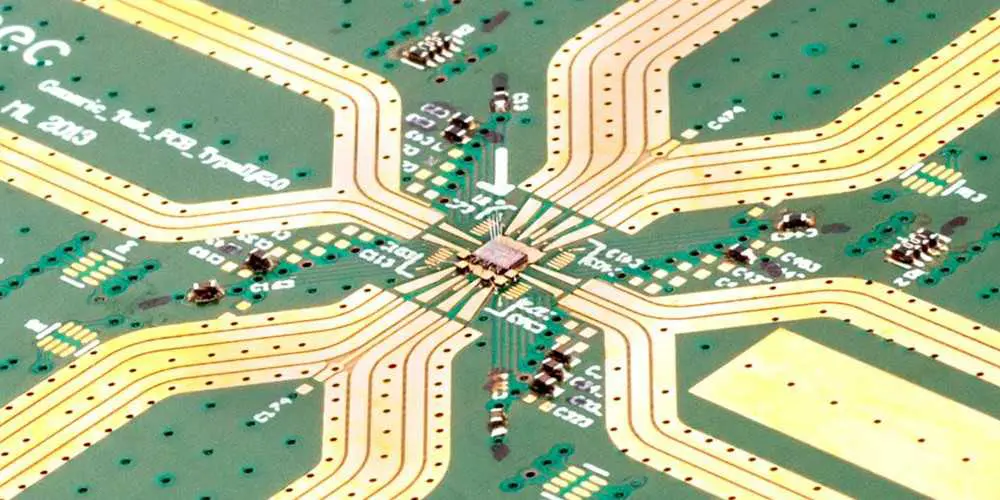
IPC-2221 (Original Version)

The original IPC-2221, released in 1998, set the foundation for modern PCB design standards. Let’s examine its key features and limitations.

Key Features of the Original IPC-2221

  1. Comprehensive coverage of PCB design aspects
  2. Detailed guidelines for material selection
  3. Electrical and mechanical design considerations
  4. Basic thermal management principles
  5. Documentation and testing requirements

Limitations and Areas for Improvement

While groundbreaking at the time, the original IPC-2221 had some limitations:

  1. Limited guidance on high-speed design
  2. Minimal coverage of advanced materials
  3. Lack of specifics on emerging technologies
  4. Outdated manufacturing process guidelines

Read more about:

IPC-2221B: Major Updates and Changes

IPC-2221B, released in 2012, brought significant updates to the standard. Let’s explore the key changes and their implications for PCB design.

Enhanced High-Speed Design Guidelines

One of the most significant improvements in IPC-2221B was the expanded coverage of high-speed design considerations. This update included:

  1. More detailed impedance control guidelines
  2. Enhanced recommendations for signal integrity
  3. Updated crosstalk mitigation techniques
  4. Improved guidance on power distribution network design

Advanced Materials and Technologies

IPC-2221B incorporated guidelines for newer materials and technologies that had become more prevalent in the industry:

  1. Expanded coverage of flex and rigid-flex PCBs
  2. Updated information on embedded passive and active components
  3. Guidelines for using advanced laminate materials
  4. Considerations for high-density interconnect (HDI) designs

Refined Manufacturing Process Guidelines

The B revision also updated manufacturing process guidelines to reflect advancements in PCB fabrication:

  1. Updated recommendations for via structures and formation
  2. Refined guidelines for surface finishes
  3. Improved guidance on board stackup design
  4. Enhanced specifications for conductor width and spacing

Environmental Considerations

IPC-2221B introduced more comprehensive guidelines for environmental factors:

  1. Expanded guidance on designing for harsh environments
  2. Updated information on thermal management techniques
  3. Enhanced recommendations for conformal coating usage

IPC-2221C: The Latest Standard

Released in 2019, IPC-2221C represents the most up-to-date set of guidelines for PCB design. Let’s examine the key updates and how they address the evolving needs of the electronics industry.

Integration of Internet of Things (IoT) Considerations

With the rapid growth of IoT devices, IPC-2221C introduced guidelines specific to this emerging field:

  1. Design considerations for low-power IoT devices
  2. Guidelines for integrating wireless communication modules
  3. Recommendations for enhancing security in IoT PCB designs
  4. Considerations for battery-powered and energy harvesting designs

Enhanced High-Frequency and High-Speed Design Guidelines

Building upon the improvements in IPC-2221B, the C revision further refined guidelines for high-frequency and high-speed designs:

  1. Updated recommendations for designs operating above 1 GHz
  2. Improved guidance on managing electromagnetic interference (EMI)
  3. Enhanced signal integrity considerations for ultra-high-speed interfaces
  4. Refined guidelines for impedance control in complex stackups

Advanced Manufacturing Techniques

IPC-2221C incorporates guidelines for cutting-edge manufacturing processes:

  1. Recommendations for 3D printed electronics
  2. Updated guidelines for additive manufacturing processes
  3. Considerations for ultra-thin and ultra-dense PCB designs
  4. Improved guidance on advanced via structures (e.g., blind and buried vias)

Sustainability and Environmental Impact

Reflecting the growing emphasis on sustainability in electronics, IPC-2221C introduced:

  1. Guidelines for designing recyclable PCBs
  2. Recommendations for using eco-friendly materials
  3. Considerations for energy-efficient PCB designs
  4. Updated guidelines for RoHS and REACH compliance

Artificial Intelligence and Machine Learning Integration

Recognizing the increasing role of AI and ML in electronics, IPC-2221C added:

  1. Design considerations for integrating AI/ML processors
  2. Guidelines for high-performance computing in PCB designs
  3. Recommendations for thermal management in AI-intensive applications
  4. Considerations for power delivery in ML-accelerated systems

Comparison Table: IPC-2221 vs. IPC-2221B vs. IPC-2221C

To provide a clear overview of the changes across versions, here’s a comparison table highlighting key aspects:

AspectIPC-2221 (Original)IPC-2221BIPC-2221C
High-Speed DesignBasic guidelinesExpanded coverageFurther refined
Advanced MaterialsLimited coverageImproved guidelinesComprehensive coverage
Manufacturing ProcessesBasic recommendationsUpdated guidelinesCutting-edge processes
Environmental ConsiderationsMinimal coverageExpanded guidelinesSustainability focus
IoT ConsiderationsNot coveredLimited coverageComprehensive guidance
AI/ML IntegrationNot coveredNot coveredInitial guidelines
High-Frequency DesignBasic guidelinesImproved coverageComprehensive guidance
Thermal ManagementBasic principlesEnhanced guidelinesAdvanced techniques
Security ConsiderationsMinimal coverageBasic guidelinesEnhanced focus

Implications for PCB Designers and Manufacturers

The evolution of IPC-2221 has significant implications for both PCB designers and manufacturers. Let’s explore how these changes affect different aspects of the industry.

For PCB Designers

  1. Expanded design possibilities: New guidelines allow for more innovative and complex designs.
  2. Increased focus on performance: Enhanced high-speed and high-frequency guidelines enable better-performing PCBs.
  3. Greater environmental responsibility: Sustainability guidelines encourage eco-friendly designs.
  4. IoT and AI readiness: New sections prepare designers for emerging technologies.

For PCB Manufacturers

  1. Advanced process adoption: Guidelines for cutting-edge manufacturing techniques encourage process upgrades.
  2. Quality improvements: Refined specifications lead to higher-quality PCB production.
  3. Expanded capabilities: Coverage of new materials and technologies opens new market opportunities.
  4. Environmental compliance: Updated guidelines help manufacturers meet evolving environmental regulations.

Challenges in Adopting the Latest Standards

While the updates in IPC-2221B and IPC-2221C bring numerous benefits, adopting these new standards can present challenges:

  1. Learning curve: Designers and manufacturers need to familiarize themselves with new guidelines and techniques.
  2. Equipment upgrades: Some advanced manufacturing processes may require new equipment investments.
  3. Software updates: Design software may need updates to incorporate new guidelines and checks.
  4. Cost considerations: Implementing new standards may initially increase design and manufacturing costs.

Future Outlook: What’s Next for IPC-2221?

As technology continues to advance, we can expect future revisions of IPC-2221 to address emerging trends and challenges in the electronics industry:

  1. Quantum computing considerations
  2. Guidelines for flexible and stretchable electronics
  3. Integration of biological and electronic systems (bio-electronics)
  4. Advanced materials like graphene and carbon nanotubes
  5. Guidelines for extreme miniaturization and 3D chip stacking

Conclusion

The evolution of IPC-2221 from its original version through IPC-2221B to the current IPC-2221C reflects the rapid advancements in PCB design and manufacturing technologies. Each revision has brought significant improvements, addressing the changing needs of the electronics industry and incorporating guidelines for emerging technologies.

For PCB designers and manufacturers, staying up-to-date with these standards is crucial for producing high-quality, reliable, and innovative electronic products. While adopting the latest standards may present some challenges, the benefits in terms of improved performance, reliability, and future-readiness make it a worthwhile endeavor.

As we look to the future, we can expect IPC-2221 to continue evolving, addressing new technologies and challenges in the ever-changing landscape of electronics design and manufacturing. By embracing these standards and the innovations they enable, the industry can continue to push the boundaries of what’s possible in electronic design.

FAQs

  1. Q: How often is IPC-2221 updated? A: While there’s no fixed schedule, major updates have occurred approximately every 7-10 years, with minor revisions in between.
  2. Q: Is it necessary to always use the latest version of IPC-2221? A: While using the latest version is recommended for access to the most up-to-date guidelines, many companies may continue using older versions depending on their specific needs and capabilities.
  3. Q: How do I get access to the IPC-2221 standard? A: The standard can be purchased directly from the IPC website or through authorized distributors.
  4. Q: Are there any free resources to learn about IPC-2221 changes? A: While the full standard is not free, IPC often provides summaries of major changes, and many industry publications offer overviews of updates.
  5. Q: How does IPC-2221 relate to other IPC standards? A: IPC-2221 serves as a foundational standard, with other standards in the IPC-2220 series building upon it for specific applications or technologies.

The Impact of Millimeter Wave PCB in High Frequency Radar Detectors Applications

Millimeter wave PCB

As technology keeps advancing, there has been a rising demand for faster network services. Telecom carriers now demand more for much faster network services. Also, consumer electronics and telecommunication devices require high-frequency circuits to perform well. Therefore, the manufacturer of these devices integrate millimeter wave PCB.

Millimeter wave PCB has contributed to the advancements in some electronic devices like computers, phones, and more. This PCB ensures faster data connection and network services in these devices.

What is a Millimeter wave PCB?

A millimeter wave PCB comprises a high-frequency circuit and a control circuit in a unit. This PCB enhances wiring freedom for high-frequency boards. Millimeter wave frequencies are crucial for communications and other applications. This is because these frequencies offer broad bandwidths.

However, it is challenging to find PCB materials that offer high performance levels for good prices at these frequencies. Millimeter wave PCBs are commonly used in automotive radars and now 5G wireless networks. However, before these frequencies can be popular, there must be low-loss circuits at frequencies like 60 and 77 GHz. Therefore, fabricating these circuits will demand for ideal circuit materials.

Choosing circuit materials at these frequencies will rely on determining the material parameters. The material parameters have a huge impact on performance. Millimeter wave is an electromagnetic spectrum ideal for use in a wide array of products such as broadband access. The millimeter wave PCB is ideal for use in various service on wireless networks. These PCBs allow higher data rates

Applications of Millimeter Wave PCB

mmwave pcb materials

Millimeter wave PCBs are widely used in several applications in the modern world. These applications include security, telecommunications, and automotive radars.

Automotive

In the technology world, autonomous driving is becoming popular. Also, it requires detecting passengers and obstruction in real time. Correct detection is crucial and decisions need to be made in a short time frame. Therefore, millimeter waves PCBs are the perfect option for detection radar.

Also, millimeter waves are available in various automotive applications like automatic lane keeping and pedestrian detection. Millimeter waves also help to communicate with other vehicles. Therefore, it improves safety.

Radar

The radar technology is one of the applications that integrates millimeter microwave. This technology integrates a property of millimeter waves known as beamwidth. Compact sized radar use sophisticated semiconductor technology. Millimeter waves PCBs are suitable for use in radar applications due to their high resolution and short range. Also, millimeter waves can easily detect objects and any changes in the environment. Therefore, this makes them a great option in surveillance and security systems.

Medical applications

According to researchers, millimeter wave technology is crucial in medical applications like acute pain treatment. Also, millimeter wave therapy utilizes frequency ranging from 40 GHz and 70 GHz. Millimeter waves serves different purposes in medicine. These include tissue regeneration and cancer treatment.

Satellite communication

Millimeter wave PCBs are a perfect option for satellite communication. These PCBs operate well with low latency at higher altitudes. Millimeter wave PCB features a much higher frequency than radio wave PCBs. Therefore, this indicates that they have the ability to carry more data.

Also, millimeter waves travel in a straight line. This makes them suitable for satellite communication. Millimeter wave PCBs have really contributed to the high performance of satellite communication in our world today.

Other Applications of Millimeter Wave PCB

  • Weather mapping device
  • Nanometer
  • Radio astronomy
  • Medical treatments
  • Snow gauge
  • Tensiometers
  • Hygrometers

Benefits of Millimeter Wave PCB

Millimeter wave PCB is widely integrated among electronic device manufacturers. Some devices deliver high throughput data.

Bandwidth and scalable capacity

The frequency of millimeter wave ranges from 26.5 to 300 GHz. This bandwidth can be as high as 273.5 GHz. Millimeter wave PCBs offer faster speed. Millimeter wave transmit signals in very focused beams and this enables several deployments in tight proximity. Also, this enables a density of about 15 times more.

Communication applications need wide bandwidths. This means the ability to handle simultaneous communication channels for a particular data rate. Due to the high data rates and wide bandwidths of these PCBs, they are ideal for use in satellite communication.

Increased resolution

Increased bandwidth and higher frequency of millimeter wave signals help to support more accurate velocity measurement. This is very crucial in radar systems and other applications.

Low latency

One of the greatest benefits of integrating millimeter wave PCBs in devices is its low latency. In terms of one-way communication, latency refers to the time a source sends a data to the time the destination receives the data packet. Millimeter waves offer higher frequencies.

 Therefore, this indicates the transmission of more data in a shorter time. A high-frequency system will feature a lower latency.  Also, low-latency is very crucial for several time-sensitive applications such as wireless augmented and automated driving systems.

Limited range and reflection

The limited range and reflections provided by millimeter wave PCBs is beneficial to telecommunications. These benefits allow the placement of several small cells near each other without any interference. Also, this allows higher bandwidth consumers in an area.

Disadvantages of Millimeter Wave PCBs

Regardless of the benefits of millimeter waves, they have their limitations. Moisture and gasses in the atmosphere absorb millimeter waves. Therefore, this minimizes the strength and range of the waves. Also, humidity and rain can minimize their propagation distance and signal strength.

A millimeter wave usually travels by line of sight and physical objects like buildings and trees can block them. Also, closeness to animals and humans affect their propagation due to the content of water. Millimeter waves have negative impacts on the brain due to their penetrating effects. Therefore, they generate EEG changes and some neurological changes in the body.

The absorption of millimeter waves in the body is a major concern. The major concern here is the heating of the skin and eyes.

Conclusion

Millimeter wave PCBs offer some benefits to some applications like telecommunication and medicine. Also, these boards feature exceptional electrical and mechanical properties that make them suitable for use in advanced circuit boards. However, these boards could be dangerous to human lives. Human bodies are reflective and as such, donโ€™t absorb much radiation from millimeter waves.

How can 5G MMWAVE PCB Benefit High Frequency Applications?

5g mm wave pcb

Millimeter wave refers to the band of spectrum having wavelengths between 30 GHz (10 millimeters) and 300 GHz (1 millimeter).  Although 5G is in the early stage, industries are currently focusing on integrating this technology and work out how to support it. Technology has advanced and the way we use web. The features we could only get in a desktop computer are now available in our palms with more advanced features.

Our mobile phones are not only the devices that utilize networks. There are other devices that share the same networks with our tablets and smartphones. These devices include internet-connected vehicles, smartwatches, and smart appliances like thermostats and refrigerators.

Millimeter Waves in 5G

Millimeter waves ensure the workability of 5G networks that offer improved reliability and speed. Also, 5G networks integrating MM wave would create opportunities to various data-heavy applications. Furthermore, it can offer enough bandwidth for the development of internet-connected devices. It can also create opportunities for other applications like traffic management, autonomous vehicles, and education.

5G is the most recent cellular network. It is the fifth generation cellular network. Also, it is the newest wireless standard that will be available for a few years. MM wave is very crucial for the future of 5G. It is laying the foundation for 5G performance. Millimeter wave helps to realize the maximum potential of 5G. Furthermore 5G mmWave reveals the capacity and fast throughput that enhances cost-efficient unlimited data plans.

MM waves in 5G can only cover indoor and outdoor environments sue to the limitations. However, it wonโ€™t cover both environments together. This means that an antenna transmitting MM waves put outdoors wonโ€™t penetrate buildings and homes to offer 5G connectivity to users inside. Also, this is the same for people who are connected to an antenna indoor.

MMWave is a crucial element and a building block of 5G system. The 5G MM Wave can offer differentiated services. Therefore, it makes it an ideal investment all mobile operators should integrate in their 5G network deployment. Also, millimeter wave is a technology integrated by 5G. It is what completes 5G. Also, the deployment of millimeter wave in 5G helps to discover immediate user experience and enjoy the benefits of network efficiency.

What is 5G MM PCB?

5g mmwave frequency pcb

5G MM PCB is a type of circuit board that integrates 5G millimeter wave. Presently, 5G is the new manufacturing and design challenges for high-frequency boards. Therefore, the 5G mm wave PCB is suitable for high-frequency applications. The PCB industry requires metrology and new imaging techniques to fabricate 5G mm PCB.

There are several manufacturing technologies poised to offer inspection and imaging capabilities required for more complex and higher quality boards for 5G. Also, mmWave refers to electromagnetic waves whose wavelengths are short. Shorter wavelengths produce higher frequency. Therefore, mmWaves signals produce high frequencies.

A 5G MM PCB provides higher frequencies in applications. In telecommunication, the 5G MM PCB plays a crucial role. Also, this offers higher frequencies and signal integrity when used in devices. Also, higher frequency signals can carry more data. This indicates more bandwidth and much faster network speeds.

Due to 5G MM PCB capabilities, devices that integrate this board can provide maximum speeds of about 4-5Gbps. However, consumer speeds can be lower.  Also, mmWaves are much faster than some wired fiber broadband connections. 5G mm PCBs are widely used across applications that require faster data connection and higher frequencies.

ย Furthermore, the integration of mmWave technology in this PCB allows faster speed data transmission. Therefore, the main highlight of this PCB is 5G mmWave. Also, this PCB provides bigger capability for users.

Benefits of 5G MM PCB

FULL PCB MANUFACTURING Quote

5G MM PCB offers higher network speed rate. Asides this benefit, 5G mmWave offers a lot of advanced benefits when used in applications.

High bandwidth

5G mmWave frequency band can deliver higher bandwidth. Also, speed rate will be higher when the bandwidth is wider. Data transfer is similar to the transportation of goods between two places. Letโ€™s say the goods transported represent the data. The distance between the starting point and the receiving point represents the electromagnetic wave.

Therefore, quick delivery of goods to the receiving point will require increasing the lanes so that more trucks can travel at one time. More lanes mean more trucks can transport goods in a unit time. Also, this is similar to the way bandwidths transmit more data. Therefore, higher bandwidth results in faster data transmission.

Higher return on investment

This is one of the benefits of 5G mmWave businesses and consumers enjoy. 5G mmWaves offers better satisfaction and user experiences for consumers and business. Also, this results in critical monetization possibilities and opportunities for operators.

Rich resources

The electromagnetic waveโ€™s frequency used becomes higher as wireless communication develops from one generation to another. 5G MM PCB must integrate more frequency resources to have a higher network speed.

Low latency

5G MM PCB offers low latency. This benefit will improve video streaming and surveillance. Also, this benefit will enable new opportunities now and in the future.

Applications and Use Cases of 5G MM PCB

5g mm wave
5g mm wave

5G MM PCBs are ideal for use in advanced manufacturing technologies. Many applications that utilize advanced mobile broadband will benefit from high network.  In addition, 5G mmWaves circuit boards are ideal for application that demand increased data capacity. Also, this circuit is ideal for mission-critical applications.

5G MM PCB is widely used in security scanners, telecommunication systems, and more. The high bandwidth provided by this PCB makes it the perfect choice for short-distance wireless transmissions. 5G MM PCBs are also crucial in the medical industry. Also, communication devices used in subway stations, factories, and offices need 5G MM PCB.  You will find 5G MM PCB in applications like:

Conclusion

You must have heard some news about 5G, maybe not for good reasons. This is because several people and companies are concerned about the effect of its bandwidth on human health. However, 5G will continue to contribute to technology evolution now and in the future. Also, the short transmission distances and high bandwidth provided by this PCB makes it ideal for use in several applications.

DipTrace Vs Geda PCB Design Software

PCB design

There are several software packages for designing circuit boards in todayโ€™s world. As the electronic world advances, so is PCB design. More advanced boards are needed for manufacturing compact and powerful electronics. The process of PCB manufacturing usually begins with PCB design.

Some PCB design software packages are very popular among PCB manufacturers. These software include Eagle, OrCad, and Altium Designer. However, there are other software packages that offer great results.  Also, it is advisable that hardware entrepreneurs and starters start with a less popular PCB design package like Geda and DipTrace.

Although these two software packages arenโ€™t as popular as some other software, they offer great features. Altium is expensive and as such, few engineers opt for this software. Most PCB developers like freelance designers, entrepreneurs, and hackers usually canโ€™t afford this software. Therefore, there are other power, yet cheaper alternatives like DipTrace and Geda. In this article, we will consider DipTrace Vs Geda PCB.

What is DipTrace?

diptrace
diptrace

DipTrace is affordable, powerful, and easy to use PCB design software. It is suitable for hobbyists. Also, DipTrace provides advanced features that help to create complex or simple multilayer PCBs from schematic to manufacturing files.

Also, this software features four different modules. One of the modules is for PCB layout while another is for schematic entry. Another module is for creating new components and the last module is for creating new landing patterns. Also, these modules are schematic capture, PCB layout, component editor, and pattern editor.

Schematic capture

The schematic capture is a PCB design tool that offers support to multi-level and multi-sheet  hierarchical schematics. Also, this tool allows you to convert circuits to a PCB. Spice export and verification enable full project analysis.

PCB layout

The PCB layout module features shape-based autorouting, 3D previewing, smart manual routing, and advanced verification. Class-to-class rules and net classes can define design rules. Also, DipTrace offers a design process which produces reports of errors on the fly before making them. You can preview the board in 3D and export for any mechanical CAD modeling.

Also, this module ensures great quality of final design by comparing source schematic and verifying net connectivity.

Component editor

The component editor module designs schematic symbols for components that are not in the library of components. Also, this module features pad numbering and bulk pin naming features that enable a designer to create multi-part complex components with several pins.

Pattern editor

The pattern editor creates PCB landing patterns for components that are new. Also, this module features 3D modeling. 3D modeling enables designers to preview the boards with attached components at any design stage.

Benefits of DipTrace

FULL PCB MANUFACTURING Quote

DipTrace is the first intuitive CAD software that offers advanced features like:

  • Smart manual routing tools
  • Multi-sheet and hierarchical schematics
  • High-speed signaling
  • Manufacturing output
  • Advanced verification and real-time DRC
  • Shape-based autorouter
  • Wide export/import capabilities
  • Real-time 3D PCB preview and STEP export
  • Good support and tutorials

Disadvantages of Using DipTrace

DipTrace has got its own drawbacks despite the benefits it offers. Also, the main drawback of this PCB design software is that it is not as standard as Eagle or Altium. For instance, you may want someone to design your PCB layout. This is quite challenging when using DipTrace.

When outsourcing a PCB layout in DipTrace, you will need to export the schematic to a PCF file. After that, you will redraw the new software package manually. Although DipTrace can import PCB layouts and schematics from Orcad or Eagle, it canโ€™t export to these formats. This is because most PCB design software packages make export to another package difficult since they donโ€™t want you to opt for another package.

What is gEDA?

gEDA is a PCB design software package used for electronic design. Also, it is an EDA (electronic design automation) application suite. gEDA is commonly used in printed circuit board design. gEDA applications is collectively known as gEDA suite.

gEDA is a great tool for schematic capture, PCB prototyping, electrical circuit design, and PCB production. Also,the gEDA project provides free software applications for electronics design. This PCB software design is highly preferred among PCB manufacturers.

gEDA is an open-source software package that feature several tools. The centerpiece of gEDA is gschem. Gschem is a schematic designer. Also, this PCB design software allows you to draw electronic schematic with the gschem tool. The electronic schematics describe the structure of a circuit.

Furthermore, these schematics comprise symbols. Symbols represent different components of the circuit and are usually obtained from a library. Also, networks represent the connection between components. gEDA features gattrib. Gattrib is a program for editing the attributes of a component. Furthermore, this PCB design software features a library of functions known as libgeda to manipulate schema and symbols.

The netlist in this software offers a flexible and sensitive utility that help to analyze the schemas to produce some results. Also, gEDA can produce BOMs and DRC reports for our schemes. There is a gsch2pcb that helps to streamline workflow.

Components of gEDA

gEDA as a design suite features the following tools:

gaf

gaf means gscheme and friends. It is the authentic gEDA project tool the team created. Also, gaf is a subset of different crucial tools. The gEDA development team maintains these tools. These tools include:

  • gschem is the primary circuit schematic capture program of gEDA. Also, gscheme features a compact user interface with several functionalities. You can draw schematics on the workspace. The different quick access buttons on the user interface allow easy use of the tool. Furthermore, the tool captures all connections and components drawn.
  • gEDA suite helps to store the schematicsโ€™ netlists for more operations.
  • Gnetlist is a program that generates netlists of different connections and components utilized in the schematic creation tool. Also, gnettlist supports over 20 netlist formats.
  • Libgeda is a library collection for gnetlist, gsymcheck, and gschem
  • Gsch2-pcb forwards annotations to the layout tool.

PCB

This is the major PCB layout program of gEDA. PCB as a component of gEDA is suitable for use across all major platforms like Windows, Unix, Mac, and Linux. Also, the tool offers several features like check design rules, trace optimizer, and schematic/netlist import.

Gerbv

This is the gEDAโ€™s gerber file viewer. Also, gerber is the major data format for circuit board design operations.

NgSPICE

NgSPICE is a PCB stimulator ideal for digital mixed-signal circuits. This tool is easy to use and understand and as well as compact.

Icarus Verilog

Icarus Verilog is a simulation and compilation tool written in Verilog data. It is a tool for source codes. Linux is the main target platform. However, it is compatible with some similar operating systems.

DipTrace vs gEDA PCB – Comparing the Difference

layout
layout

DipTrace and gEDA are both PCB design software packages. However, there are some differences between these software packages. DipTrace comes in different prices for various packages. The cheapest version is the DipTrace Sarter is available for 75 dollars. DipTrace Full provides unlimited signal layers and unlimited pins for $895.

DipTrace versions all feature humongous parts library. Also, gEDA offers huge libraries of components. gEDA is more expensive than DipTrace. DipTrace is budget friendly and as such, it is ideal for hobbyists and freelance engineers. The user interface of gEDA is more intuitive than DipTrace.

DipTrace feature four important modules for PCB design. gEDA features several components like Gerbv, gaf, and NgSPICE. These components are all crucial in ensuring good PCB design.

Some Crucial Criteria for PCB Design Software

There are diverse PCB design software packages available. Some packages donโ€™t offer the feature you need. Therefore, you need to consider some crucial factors when choosing PCB design software.

Ease of use

This is a critical feature when choosing PCB design software. DipTrace is a great software package in terms of ease of use. Integrating this software for your PCB design will help a lot. With DipTrace, you can start designing your PCB as soon as possible with a minimal learning curve. You donโ€™t need to waste time learning how to use the software. Also, Geda is a good choice too. Geda features a nice interface for both beginners and experts.

Cost

DipTrace is one of the most affordable PCB design software packages you will ever come across. This software is just half the price of Eagle or one-eight of Altiumโ€™s price. Geda is a good option when considering budget-friendly software. DipTrace offers a low or no barrier to entry since you can start with its Starter version.

Libraries

Both Geda and DipTrace feature huge libraries of components. Also, a large library is crucial since designing new components can lead to errors that any verification tool wonโ€™t capture. However, you will need to design some custom components regardless of the package. Although Eagle and Altium offer huge libraries, DipTrace and Geda feature extensive libraries.

Conclusion

The gEDA and DipTrace PCB design software packages are very efficient and make PCB design easier. When it comes to DipTrace vs gEDA PCB design software, both software packages are ideal for use. This is because they offer a good user interface which makes it easy for beginners to understand how the software works.

Thin Film Circuit Board: A Detailed and Comprehensive Guide on Thin Films

Arlon 45NK PCB

In this present scenario, the thin film circuit boards have evolved as one of the most important aspects of human life. Almost every field comes with the involvement of thin films in it; it is a solid fact that canโ€™t be denied under any given situation. In the year 1912, the first use of thin films was witnessed.

Thin-film technology uses microsystem technology processes and semiconductors in order to pave the way for circuit boards on organic or ceramic materials. The metal disposition method of this particular technology, followed by its top-notch flexibility, sets it apart from printed circuit board technology.  

The substrates or interconnection carriers in thin-film technology allow connection densities, high-precision geometrics of insulators and conductors material, and excellent thermal conductivity. As a result, these excellent technologies bless individuals with maximum reliability in no time.

Since the substrates in thin film technology are potent enough to deliver appropriate technical solutions, they generally entail higher costs when compared to thick-film substrates and printed circuit boards.

Keep reading this article to grab valuable insights about its wide range of applications, types, and uses. Stay tuned till the very end.

What Is the Morphology and Structure of Thin Films?

Thin film properties and microstructures solely depend on deposition parameters, growth mechanisms, and various techniques that are employed during the manufacturing procedure. Check out the three types of microstructures stated below in this article:

  • Polycrystalline: It forms micro or nano crystallites that come in varying sizes
  • Amorphous: It forms crystalline lattice in a perfect manner
  • Epitaxial thin films: It tends to form a solid crystalline film that, too, with latticework

The thin-film applications solely rely on the thin-film morphology, which in turn, depends on a broad range of factors. Some of them include the following:

  • Atom absorption
  • Deposition parameters
  • A flux of vapor and atoms
  • Type of material
  • Film thickness
  • Growth structure

What Are Some of the Benefits of Thin Film Technology?

Go through the unparalleled benefits of thin film technology mentioned below in this write-up:

โ— It Comes with a Low Cost

When compared to the thick film circuit, these thin film circuits come with lower costs. According to research, it is quite evident that the overall cost of thin film circuits is as less as 10% to 20% than thick ones.

โ— It Comes with Low Power Consumption

It is one of the major reasons why these thin films are preferred over thick film technologies.

What Are the Different Types of Thin Films?

FULL PCB MANUFACTURING Quote

Given below are some of the types of thin films; check out all of them at a quick glance right away:

Optical Thin Films

Optical thin films are used for creating:

  • Anti-reflective or reflective coatings
  • Displays
  • Solar cells
  • Photodetector arrays
  • Waveguides
  • Memory discs

Electronic or Electrical Thin Films

These are used to manufacture the following:

Magnetic Thin Films

The magnetic thin films are used in memory discs.

Thermal Thin Films

Thermal thin films are used to create heat sinks and barrier layers.

Mechanical Thin Films

  • The mechanical thin films are nothing but a tribological coating that is used to prevent wear and tear.
  • It imparts micro-adhesion and hardness.
  • It takes pure advantage of micromechanical properties

What Are Some of the Thin Film Circuits?

Take a look at the types stated below:

What Are the Different Uses of Thin Films in Everyday Life?

Letโ€™s dig deeper to uncover some of the common uses of thin films in your everyday life. Take a quick look at the pointers mentioned below:

โ— Use of Thin Film in a Semiconductor

The discrete semiconductor devices, along with integrated circuits, are manufactured from a bunch of thin films of semiconductor, conductive and insulating materials. This exclusive technology has boosted the possibility of miniaturization of a plethora of semiconductor devices such as diodes, BJTs, MOSFETs, and FETs.

โ— Use of Thin Film in Optoelectronics

Optoelectronics is yet another crucial field where thin film technology has paved its way in the best possible manner. Several individuals have used this thin film technology with an approach to produce batteries that are inserted into the chips.  

โ— Use of Zinc Oxide-Based Thin-Film Applications

ZnO or zinc oxide thin film applications are used in various industries such as optical, thermal, electrical, and magnetic. But, semiconductor coating and devices involve the major use of ZnO thin films. Some of the other applications include:

  • LED
  • OLED
  • Displays
  • Gas sensors
  • Solar cells
  • Photodetectors
  • Biosensors
  • Lasers

ZnO is a popular option since it is readily available, chemically and physically stable, comes with incredible conductivity, and is inexpensive in nature.

โ— Uses of Thin Film in Combating Wearing and Corrosion

Thin films tend to contribute a lot in protecting the metallic parts, thus combating their corrosion in the best possible manner. Several possessions such as wrist watches, jewelry, and knives are safeguarded with proper coating in order to deal with corrosion.

What Are Some of the Best Thin Film Coatings?

Translucent PCB

Check out the different kinds of thin film coatings stated below in this article:

TCO Coatings

TCO, or Transparent Conductive Oxide, is a type of thin film that is used in the field of electronics. You can mainly find them in display space and optoelectronics. Check out some of the common applications of TCO coatings:

  • Plasma screens
  • LCDs or Liquid crystal displays
  • Organic LEDs
  • LEDs
  • Photovoltaics or Solar Cells
  • Touch Screens
  • Strain gauges
  • Mirrors and heated windscreens
  • Sensor coatings

Biocompatible Hard Coatings

Biocompatible hard coatings are typically used in the medical field. Their core aim is to boost health outcomes and safeguard implanted devices in this highly sensitive market. Some of the examples of biocompatible coatings are:

  • Titanium aluminum nitride
  • Titanium nitride
  • Titanium carbo-nitride
  • Chrome nitride

DLC Coatings

Diamond-like carbon coatings or DLC are popular for their top-notch properties. Its lubricity, hardness, and scratch and chemical resistance properties are beyond remarkable. Some of the common uses of DLC coatings are:

The Bottom Line

These thin film circuit boards can be fitted easily in various areas. Both the fields of industrial applications and consumer electronics enjoy great benefits while using these thin-film technologies.

How to Connect and Configure the Arduino IOT Cloud

Arduino IOT

IoT, which is also called internet of things can be described as a network of some physical things, which connects to the internet. This thing can also be referred to as IoT device.

 These IoT devices help in sending and receiving data to and from the internet. Furthermore, these IoT devices will be able to exchange the data with themselves through the internet.

How can you connect the Arduino to your Internet?

One significant task when you are making IoT devices is making use of Arduino to help connect Arduino to your internet. The common ways include

  • Lora โ€“ here, you will need Lora gateway
  • GPRS/5G/4G/3G
  • ZigBee โ€“ Here, you will need a ZigBee gateway
  • BLE or Bluetooth โ€“ this requires a Bluetooth gateway
  • Ethernet
  • WiFi

Of all the methods highlighted above, the most frequently used is the Ethernet and WiFi. They are also the most secure, simple, and popular. They also involve third parties for functional and analytical purposes. Majority of those smart home products we use are making use of WiFi. Also, a good number of industrial IoT devices also make use of Ethernet.

Furthermore, for the bluetooth, you can utilize the smartphone to serve as your bluetooth gateway. An example is a bluetooth tracking device called TrackR bravo. It makes use of the smartphone to serve as a Bluetooth gateway for the โ€œcrowd locateโ€.

What are the Applications of the Arduino IoT?

arduino iot projects

Generally, during IoT application, your Arduino helps in collecting data from the devices and sensors and then sends it to the internet. Also, it receives data from your internet and websites tohelp in controlling the actuators and motors. Furthermore, it will show you personalised advertisement. IoT applications can be grouped in these types:

  • Monitoring Arduino through PC or smartphone
  • Controlling Arduino through PC or smartphone
  • Arduino helps in collecting the sensorโ€™s data as well as send it onto the database
  • Also, Arduino collects the data of the sensor and also send onto the IoT cloud
  • Arduino helps in detecting the event. It also sends notification through phone call, SMS, Email, and push notification.
  • Also, Arduino interacts and deal with some smart speakers such as Google Home, Amazon Echo Dot.
  • Arduino helps in interacting automatically with some other devices making use of some protocol like Modbus TCP.
  • Also, Arduino functions as the gateway. This forms a bridge in-between the other devices, as well as the internet.

Getting Started with the Arduino IoT Cloud

This is an online platform, which makes it very easy for the creation, deployment, and monitoring of the IoT projects. The connected devices globally are increasing in billions yearly. This is a platform, which permits anyone to help in creating the IoT projects, having a unique user-friendly interface. It also serves as a complete solution for writing code, configuration, visualization, and uploading.

Here, we will consider some of the components of Arduino IoT cloud. Also, weโ€™ll consider a usual and general overview. However, if you really wish to get started as well as explore it by yourself, this is very fine. You may always visit this tutorial to get more information.

The IoT Cloud Documentation

Furthermore, the Arduino Cloud also offers different documentation pages available. Here, you will find some important and popular pages:

  • You will be able to find all the articles and tutorials by visiting their documentation page
  • Also, for the list of features, technical overview, as well as the API guide, then check the cheat Sheet of the Arduino IoT Cloud.
  • For the SDK and API documentation, check the Arduino IoT Cloud API developer reference

What are the Features of the Arduino IoT Cloud?

Here are the different features of the Arduino IoT cloud

Data Monitoring: This helps you learn ways to monitor the sensor values of the Arduino easily via a dashboard.

Scheduler: This helps in scheduling jobs to go either on or off for some specific time period. This could be hours, minutes, and hours.

Variable Synchronization: This allows users to be able to sync the variable across the devices. This enables communication between these devices with very minimal coding.

Webhooks: This incorporates your project with a different service like IFTTT

Over the air uploads: Helps in uploading the code onto the devices that are not connected onto your computer.

Dashboard Sharing: This helps in sharing your data with different people all over the world.

Amazon Alexa Support: This makes the voice of your project controlled via the integration of the Amazon Alexa.

What are the Compatible Hardware with the Arduino IoT Cloud?

To make use of the Arduino IoT Cloud, there is a need to have a board that is cloud compatible. Also, you will choose between making use of the official Arduino board, as well as a board that is based on the ESP8266 / ESP32 microcontroller. This Arduino IoT Cloud presently supports you to connect through WiFi, mobile networks, and LoRaWAN (through the things network).

All the Arduino boards that are cloud compatible includes some hardware secure elements like ECC508 cryptochip. Here, you will be able to store your personal security keys. Also, the Arduino boards can only support a frequency band of 2.4 GHz for the transmission of data.

The boards below help to connect the Arduino IoT Cloud through WiFi. These include:MKR WiFi 1010, MKR 1000 WiFi, Nano 33 IoT, Nano RP2040 Connect, Nicla Vision, Portenta H7 Lite, and Portenta H7.

In addition, connection through WiFi is the easy option, and you can enter your credentials safely during a projectโ€™s configuration. This connection type is best for the low-range projects. Here, you will connect the board to the Arduino IoT cloud through your school, work, and home router.

LoRaWAN

These boards help to connect the Arduino IoT Cloud through the Things Stack. This is a Network Server that help to connect to thousands of gateways. Furthermore, connection through LoRaWAN is necessary for the low-power projects in the urban and remote areas whereby the WiFi as well as other well-known types of connectivity are not present.

Also, the MKR WAN boards are also equipped using the LoRa radio module. Furthermore, it has an antenna slot. With the best low-power configuration, it becomes possible for the board to send the data onto the cloud for some months on just one battery.

NB-IoT / GSM Boards

Also, the MKR NB 1500 ad the MKR GSM 1400 needs a SIM card to help connect into the cloud. This helps in communicating over the different mobile networks.

Also, you can consider the connection via mobile networks in the remote areas where there is no WiFi, neither are there in mobile projects like cargo tracking.

ESP8266 and ESP32

Arduino IoT Cloud backs and supports different third party boards. This is based on the ESP8266 and ESP32 microcontrollers having support for the WiFi. In order to set them all up, just choose the 3rd party option present in your device setup.

Support for the Arduino IoT

If the user has any issues while working with the Arduino IoT cloud, then you can check some troubleshooting issues and then get some information on the different features using their Arduino Help Center. Anyway, if you wonโ€™t be able to get the answer youโ€™re searching for, you can always ask us with any question.

Configuration Process of the Arduino IoT Cloud

Industrial-IoT-Devices

The setting up of the Arduino IoT Cloud, and accessing the features available deals with some steps. Letโ€™s consider them.

Create your Arduino Account

In order to start making use of the Arduino IoT Cloud, the first thing you need to do is to sign up. If you have already done so, all you need to do is to log in.

Go to your Arduino IoT Cloud

Once you are done signing up, you can visit the Arduino.cc page and gain access into the Arduino IoT Cloud. This is possible by clicking the four dots present on the topmost right corner of the menu.

Configure the Device

You can add devices easily and link it to a Thing. This Arduino cloud needs you to install the Arduino agent. This process of configuration is easy and quick and you can achieve this by searching on the Thing overview and then tapping on โ€œselect device.โ€

Creation of Variables

The created variables will be generated automatically into a specific sketch file. You can choose from different files like char, long, Boolean, float, and int. You will also find variables like luminance, velocity, and temperature.

Connect to a Specific Network

You must connect. When you connect to your internet network, tap โ€œconfigureโ€. Put in your credentials and then click on โ€œsaveโ€. You can also generate this information in the sketch file.

Editing your sketch

Now, there are configured variables, network settings and devices. Now, we can start with the programming of the devices as well as editing of the sketch

Creation of a Dashboard

Once you are done configuring the device and the network, created the variables, finished the sketch and uploaded your code, then you can continue. This is creating dashboards.

Conclusion

The Arduino IoT cloud is very useful in different applications. This is why it is necessary to learn its features and how to configure it from this tutorial.

PCB Design Course: Learn The Art Of PCB Design

Altium PCB design process

Students struggle with PCB design courses. PCB design is daunting and confusing for many new PCB designers. PCB design is highly technical and requires a lot of knowledge, research, trial-and and-error. It also demands hard work that can be discouraging especially for beginners.

There are a number of sites who provide training courses on PCB design to become a PCB designer. You can choose any site for PCB design courses as per your needs. But this short and free-of-cost course help students to easily understand insight working process and how it applies to practice.

With this free course, learn everything you need to know about PCB design in a fraction of the time. The course offers step-by-step instructions on PCB design from basic knowledge, schematic diagram to the final PCB output. Sounds great? Read on to find out!

What Is PCB Design Course?

layout
layout

Here comes introduction of PCB design/ electronic circuits course. It taught students about fundamentals and the basics of printed circuit board design. This PCB design resources teach students how to use CAD software and how to create a PCB layout using it.

This class enhance the knowledge skills of newbies to grow up in the electronics industry.

PCB Design Course Applications

PCBs provide physical protection and act as the connecting platform for different electronic components. They create a lot of opportunities that have a reasonably good growth status worldwide.

  • Experienced engineers who need a system-level view of product design.
  • Radio frequency design engineering
  • PCB design/ electrical engineer
  • Electromagnetic compatibility engineering
  • Electronics communication engineers

Step by Step Process Of PCB Layout Design

Down below you will get in detail insights on PCB desgin. Lets Dig in deeper!

Introduction to PCB Design Softwares

You have access to different PCB design tools/software such as Ansys, EasyEDA, and EAGLE. You can use any of these software/ tools to design PCB as per your expertise. But one software/ tool that is popular in designing PCB is Altium.

Altium Designer is a cutting-edge PCB design tool. Altium is the product of Altium Limited. You can use Altium Designer on both old/ new computers and it’s clear that this tool is covering all of the bases.

Altium includes HDL design capture, signal integrity analysis, circuit simulation, FPGA based embedded system design and development. You can access the Altium tools to support 3D modeling and track length tuning.

Beyond all this, PCB designers can also customize the Altium Designer environment to fit your needs in other ways. Now we examine how to create a schematic diagram and generate files for a PCB design using Altium Designer.

Design Process In Altium Designer

ยท Scheme Design

Before creating the actual design of a product, you need to do the following manually. This include Preparation of scheme design, the diagram of circuit, and circuit plan basic module. PCB designer will apply a simple design as an example to indicate the PCB design process.

ยท Schematic Design Of Circuit

With a detailed schematic and fine PCB design, it can finally come to use! A schematic diagram is the foundation of PCB design, It correlates with the fact that any mistakes made in the schematic diagram could still show up on printed circuit boards. It’s always the first step to figuring out the accuracy of PCB design.

ยท Establishment Of Schematic Diagram

1. Open AND Run Altium Designer Through User Interface.

The first step in Altium designer is to click File and then click New, followed by Project. Before you can get started by giving this file a name and designating its engineering classes. Engineering file establishment is convenient because it allows PCB designer to administer a number of files in one location.

It includes PCB design files (.PCB), schematic diagram symbol files (.schlib), schematic diagram files (.SCH), and PCB packaging files (.pcblib). Once you’ve translated and made edits to your schematic diagram, a netlist will be created in PCB that is associated with the original schematic.

2. Establishing symbols for Schematic diagram

To create a layout in an engineering file, first, click File, then New. Pick Libraries, then Schematic Library; a list of schematics will appear. It is important to set up the required schematic symbols.

Throughout this circuit in Altium Designer, the LED, switch, and socket resides, and the symbols for these components have been maintained. If you want to manufacture a design that meets all your requirements, it’s best to build your own design library.

In reality, most engineers utilize the built-in library. When building a library, PCB designers have to find specifications of material that correspond to the design. Your design can enforce pin names and symbols like the anode and cathode on an LED, or a transistorโ€™s three terminals.

3. Establishment Of Printed Circuit Board Packaging.

Click File, select New, and then Libraries. Select PCB libraries in the .pcblib format. Well-established PCB packaging is an important part of manufacturing PCBs. It is important to be mindful of the difference between the anode and cathode, as well as to recognize their individual symbols.

Apart from this, there are other important details that you should take into consideration. As an example, a lot of attention has to be placed on the QFP package because a back view is generally provided with specifications.

So, it’ll make things quicker when establishing the PC board package. On the other side, the established library is the opposite. The padding for this component and the size of the via is also according to the principle’s techniques.

In Altium, component via size is determined by the diameter of the pins while hole pad size is determined by the size of its via.

Let’s take the package of LED as an example. Assuming the LED has a diameter of 3mm, pin spacing of 2.54mm, and the thickness of the pins at 0.6mm. In printed circuit board Libraries’ interface:

a. Placement Of Pad

โ‘ . Pad Via diameters = pin diameter + 0.9mm + 0.3mm;

โ‘ก. A circle is perfect for a pad. Its diameter is equal to diameter of pad via 0,9mm + 1.2mm = 2.1mm (typically one sideboard + 1.2mm while two sideboard + 1.0mm);

โ‘ข. If PCB designer use SMT, they can place Pad at the top layer;

โ‘ฃ. Coordinate placement: X (-1.27mm) and Y (0);

โ‘ค. 1 pin explained as a pad ( 1 is as a Designator);

โ‘ฅ. The second pad is placed in the same way, with a different coordinate placement than: X=1.27mm and Y=0. You can design a second pad by 2 pins with a designator of 2.

To create a convenient solution for manufacturing, you have to set the original point located in the center of the component. This is why coordinates 1.27 and -1.27 are respectively mentioned in the text above.

b. After Placing Pad The Silkscreen Is Drawn

c. Save And Name The File

4. Set up a connection between printed Circuit board pACKAGE AND SCHEMATIC SYMBOLS

pcb design tips

You can connect the PCB package with the corresponding schematic symbols from the component attribute list. After setting up the PCB package libraries and schematic symbol libraries. you have to translate and edit the corresponding libraries too.

Altium Designer can automatically check the component information and detect any possible errors. If it finds any, it will prompt you with an error message.

5. Schematic Capture Or Drawing

To create a schematic drawing, you need to Click File>>New, then select the schematic inside the drop-down list. In the schematic interface, you can choose a range of formats for standard drawing like A4 drawing: depending on your project.

Once you’ve found the schematic symbols, simply insert them into the schematic interface. At last, ensure that pins are connected with electric power distribution lines to retain signal integrity. Once the schematics for a design have been completed, it can be checked for errors automatically.

On the schematic in Altium designer, right-click in the area with the completed diagram and put your cursor over compiled document ***.Schdocโ€ in the popup bar.

ยท Establishment Of PCB Design Files

In Altium, Go to your services file, then click File, New, and select PCB. After that input a filename and save it.

  1. You can adjust the size of the sheet frame for PCB to meet the needs of your system structure. Mechanical 1 is used for creating a frame for PCB, the size of the PCB in the example is 62x55mm.
  2. Lead component info. The component information or data you see in the netlist and schematic capture is stored in PCB. Click Design, then Update your PCB designs Document.

a) Once students make changes here, they will be validated and saved automatically.

b) If you want to manually you can do so by clicking Validate Changes and then Execute Changes.

  • Setting Of Design Rules. In this section, you will make adjustments to the distances between lines and their widths.
  • A good layout is half of the job. Students should remember layout rules that include:

a) One possible solution is to fix the location holes.

b) Avoid moving components until they are ready to place in the final configuration. This will help prevent them from being moved by other components and ruining their final location.

c) It is often best to layout from larger components to smaller ones.

  • Routing. Routing is where you’ll connect your lines, vias, and components together on a PC board.

a) Interactive Routing: Click place and then interactive routing with a cursor that looks like a cross, which can be used to follow the route.

b) Auto Routing: Ensure that “Click Auto Route” is selected and then all of your routes will be automatically calculated.

  • Add Copper And Teardrop Coating. If you’re looking to build more strength between your lead and pad or between your through-hole vias, adding a copper and teardrop coating is an excellent way of achieving this.

a) Generally, the coating should be applied to the PCB designs after routing.

b) Ordinarily, the copper coating is usually applied to ground lines to meet the increasing need for stable power and signal transmission due to their low impedance levels.

  • Design Rule Check. Firstly tap Tools then Design Rule Check. Check the error log in your design report to see the types of errors you need to fix. Students can then modify their PCB design process accordingly, and run DRC until no more errors are found on the report.

Output Of Printed Circuit Board Files:

PCB design training courses present such output:

  • Gerber file: It is provided to PCB manufacturers.
  • Assembly diagram: You can use it as an instruction manual.
  • Component coordinates: It allows the workshop to just mount the components automatically on the machine.
  • BOM: It is offered to the supplier and production department.
  • If necessary, other files in other types of formats can be created.

Conclusion

These days PCB design/fabrication require student and instructor to keep up pace through developing innovative design for future endeavors. The lessons taught on PCB design course will surely be helpful. Now you need to test yourself through practice.

We have discussed in detail process on PCB design. After this course you are able to design your PCB board with the least amount of error. In case if you have any queries or interested in learning more about PCB desgin feel free to reach out or comment below. We would love to help you.

Quick Turn PCB Manufacturing: 24-Hour Prototyping & Production Services

Get your PCBs manufactured in as little as 24 hours without compromising quality. RayMing delivers rapid PCB prototyping and small-volume production services with over 20 years of manufacturing excellence, helping engineers accelerate their time-to-market while maintaining the highest quality standards.

Whether you need emergency prototypes, pre-production testing, or full-scale manufacturing with tight deadlines, our quick turn PCB services provide the speed and reliability your projects demand. Experience the perfect balance of rapid turnaround, superior quality, and competitive pricing that has made RayMing a trusted partner for thousands of engineers worldwide.

What is Quick Turn PCB Manufacturing?

Quick turn PCB manufacturing is a specialized fabrication process that delivers printed circuit boards in dramatically reduced timeframesโ€”typically 24 to 72 hoursโ€”compared to standard manufacturing cycles that can take weeks. This accelerated approach revolutionizes product development by enabling rapid prototyping, faster design iterations, and emergency production runs without sacrificing quality or reliability.

Quick Turn vs Standard PCB Fabrication

Standard PCB Manufacturing:

  • Lead times: 2-4 weeks
  • Optimized for large volume production
  • Lower per-unit costs for high quantities
  • Less flexibility for design changes

Quick Turn PCB Services:

  • Lead times: 24-72 hours
  • Optimized for prototypes and urgent orders
  • Premium pricing for expedited service
  • High flexibility for rapid iterations
  • Same quality standards as standard production

The key difference lies in manufacturing prioritization and streamlined processes. Quick turn PCB manufacturers like RayMing maintain dedicated production lines, pre-stocked materials, and optimized workflows specifically designed for rapid fabrication without compromising on quality control measures.

Industries That Benefit from Fast PCB Services

Consumer Electronics: Smartphone manufacturers, wearable device companies, and IoT developers rely on quick turn PCB services for rapid prototyping and market testing of new products.

Medical Devices: Medical equipment manufacturers require fast PCB prototyping for life-critical devices where rapid development cycles can bring life-saving technologies to market sooner.

Automotive & Aerospace: These industries use quick turn services for testing advanced driver assistance systems (ADAS), electric vehicle components, and avionics prototypes.

Telecommunications: 5G infrastructure development, network equipment prototyping, and communication device testing demand rapid PCB fabrication capabilities.

Quick Turn PCB Capabilities & Specifications

Turnaround Time Options

24-Hour Express Service:

  • Simple 1-2 layer boards
  • Standard FR-4 materials
  • HASL or ENIG surface finish
  • Prototype quantities (1-50 pieces)

48-Hour Fast Track:

  • Up to 6-layer boards
  • Multiple material options
  • Various surface finishes
  • Small production runs (1-200 pieces)

72-Hour Standard Quick Turn:

  • Complex multilayer boards (up to 16 layers)
  • Specialized materials (Rogers, Polyimide)
  • Advanced surface finishes
  • Medium production volumes (1-500 pieces)

Layer Count & Complexity Handling

Layer CountQuick Turn CapabilityTypical Applications
1-2 Layers24-48 hoursSimple prototypes, LED boards
4-6 Layers48-72 hoursConsumer electronics, IoT devices
8-12 Layers72 hours – 5 daysTelecommunications, computing
14-16 Layers5-7 daysHigh-speed digital, servers

Material Options for Rapid Fabrication

Standard Materials (24-48 hour capability):

  • FR-4 Standard and High-Tg
  • CEM-1 and CEM-3
  • Aluminum-backed boards
  • Standard prepreg options

Specialized Materials (48-72 hour capability):

  • Rogers RT/duroid series
  • Polyimide flexible materials
  • PTFE-based substrates
  • High-frequency materials

Technical Specifications:

  • Minimum trace width: 0.1mm (4 mil)
  • Minimum via size: 0.2mm (8 mil)
  • Layer count: 1-16 layers
  • Board thickness: 0.4mm – 3.2mm
  • Maximum board size: 610mm x 1220mm

Quick Turn PCB Manufacturing Process

Design File Submission & DFM Review

The quick turn PCB process begins when you submit your design files through our secure online portal. Our engineering team performs a comprehensive Design for Manufacturability (DFM) review within 2 hours of file submission, ensuring your design meets all technical requirements for rapid fabrication.

Required Files:

  • Gerber files (RS-274X format)
  • Excellon drill files
  • Pick and place files (for assembly)
  • Bill of Materials (BOM)
  • Assembly drawings and specifications

Our automated DFM software instantly checks for potential manufacturing issues while our experienced engineers verify design intent, material compatibility, and manufacturability constraints. Any concerns are immediately communicated to prevent delays in the production process.

Rapid Prototyping Stage

Quick turn PCB prototyping serves as the critical first step in validating your design before committing to larger production runs. During this stage, we manufacture small quantities (typically 5-50 pieces) that exactly represent your final product specifications.

Prototype Validation Benefits:

  • Early detection of design flaws
  • Functional testing capabilities
  • Component fit verification
  • Signal integrity validation
  • Thermal performance assessment

Our prototype PCBs undergo the same rigorous quality control procedures as production boards, including automated optical inspection (AOI), electrical testing, and dimensional verification. This ensures that prototype results accurately predict production performance.

Pre-Production Testing & Validation

The pre-production phase involves manufacturing larger quantities (100-1000 pieces) to validate manufacturing processes and identify any potential issues before full-scale production. This critical stage helps optimize manufacturing parameters and ensures consistent quality across production volumes.

Key Pre-Production Activities:

  • Manufacturing process optimization
  • Yield analysis and improvement
  • Quality system validation
  • Supply chain verification
  • Cost optimization strategies

During pre-production, we conduct comprehensive electrical testing, including flying probe testing for prototype quantities and bed-of-nails testing for larger volumes. This thorough testing approach ensures that every board meets your specifications before moving to full production.

Full Production & Quality Control

Full production quick turn PCB manufacturing maintains the same accelerated timeline while scaling to meet your volume requirements. Our production facilities operate 24/7 to ensure rapid delivery of high-volume orders without compromising quality standards.

Production Quality Controls:

  • 100% AOI inspection
  • Statistical process control monitoring
  • IPC-A-600 compliance verification
  • Final electrical testing
  • Packaging and shipping verification

Advanced Technologies for Quick Turn Assembly

Surface Mount Technology (SMT) for Fast Assembly

Our state-of-the-art SMT lines feature high-speed pick-and-place machines capable of placing over 50,000 components per hour with placement accuracy of ยฑ25 microns. This advanced equipment enables rapid assembly of complex PCBs while maintaining exceptional quality standards.

SMT Capabilities:

  • Component sizes: 01005 to large BGAs
  • Fine-pitch components: 0.3mm pitch and smaller
  • High-speed placement: Up to 50,000 CPH
  • Placement accuracy: ยฑ25 microns
  • Component types: Resistors, capacitors, ICs, connectors

Our quick turn SMT assembly process includes automated solder paste printing, component placement, reflow soldering, and comprehensive quality inspectionโ€”all optimized for rapid turnaround without sacrificing reliability.

Through-Hole Assembly Capabilities

For components requiring through-hole assembly, our selective soldering systems and wave soldering equipment provide precise, reliable connections for quick turn projects. Our skilled technicians also perform hand soldering for prototype quantities and specialized components.

Through-Hole Services:

  • Automated selective soldering
  • Wave soldering for high volumes
  • Hand soldering for prototypes
  • Mixed technology assembly
  • Component lead forming and preparation

Mixed Technology PCB Assembly

Many modern PCBs require both surface mount and through-hole components. Our mixed technology assembly capabilities seamlessly integrate both mounting methods in a single, streamlined process optimized for quick turn production.

Mixed Assembly Advantages:

  • Single-pass manufacturing process
  • Reduced handling and potential damage
  • Optimized thermal profiles
  • Comprehensive testing procedures
  • Faster overall assembly times

Quality Assurance in Quick Turn Manufacturing

IPC Standards Compliance

All quick turn PCB manufacturing at RayMing strictly adheres to IPC standards, ensuring that accelerated production timelines never compromise quality or reliability. Our quality management system maintains compliance with IPC-A-600 (acceptability standards) and IPC-6012 (qualification standards).

Key IPC Standards:

  • IPC-A-600: PCB acceptability standards
  • IPC-6012: Qualification and performance specifications
  • IPC-2221: Generic standard for PCB design
  • IPC-A-610: Electronic assemblies acceptability
  • J-STD-001: Soldering requirements

Our quality engineers continuously monitor compliance through statistical process control, ensuring that every quick turn PCB meets or exceeds industry standards regardless of production timeline.

AOI and Electrical Testing Procedures

Automated Optical Inspection (AOI) systems provide 100% inspection coverage for all quick turn PCBs, detecting manufacturing defects that could affect performance or reliability. Our advanced AOI systems use high-resolution cameras and sophisticated algorithms to identify issues invisible to manual inspection.

Testing Procedures:

  • Pre-etch AOI for substrate quality
  • Post-etch AOI for trace integrity
  • Solder mask inspection
  • Silkscreen verification
  • Final dimensional inspection

Electrical Testing:

  • Flying probe testing for prototypes
  • Bed-of-nails testing for production
  • In-circuit testing (ICT) when required
  • Boundary scan testing capabilities
  • Functional testing for assemblies

Materials Certification & Traceability

Every quick turn PCB project includes complete materials certification and traceability documentation. We maintain detailed records of all materials used, including substrate certifications, solder certifications, and component traceability for aerospace and medical applications.

Certification Documentation:

  • Material test certificates (MTCs)
  • RoHS compliance certificates
  • UL recognition documentation
  • IPC test coupons and reports
  • Statistical process control data

Quick Turn PCB Pricing & Cost Factors

24 layer pcb

Factors Affecting Quick Turn Costs

Quick turn PCB pricing reflects the premium value of accelerated manufacturing while remaining competitive within the rapid fabrication market. Several key factors influence pricing for expedited orders:

Primary Cost Factors:

  • Turnaround time requirements (24hr premium vs 72hr)
  • Board complexity and layer count
  • Panel utilization efficiency
  • Material requirements and availability
  • Surface finish specifications
  • Testing and inspection requirements

Volume-Based Pricing:

  • Prototype quantities (1-50): Premium pricing
  • Small production (51-250): Moderate premium
  • Medium volumes (251-1000): Reduced premium
  • Higher volumes: Near-standard pricing

Cost Comparison: Quick Turn vs Standard

Service TypeLead TimeCost MultiplierBest For
24-Hour Express1 day3.0-4.0xEmergency prototypes
48-Hour Fast2 days2.0-2.5xUrgent testing needs
72-Hour Quick3 days1.5-2.0xAccelerated development
Standard Production2-3 weeks1.0xHigh-volume production

Volume Pricing for Rapid Orders

Our transparent pricing structure ensures competitive costs even for expedited orders. Volume discounts apply to quick turn services, making rapid fabrication economical even for larger prototype runs.

Price Match Guarantee: If you find a lower price for equivalent quick turn PCB services, we’ll match or beat that price while maintaining our superior quality standards and reliable delivery performance.

Industries & Applications for Quick Turn PCBs

Consumer Electronics Prototyping

The consumer electronics industry drives significant demand for quick turn PCB services, particularly for smartphone accessories, wearable devices, and smart home products. Rapid prototyping enables faster product development cycles and quicker market entry.

Typical Applications:

  • Smartphone and tablet prototypes
  • Wearable device PCBs
  • IoT sensor boards
  • Consumer audio equipment
  • Gaming peripherals and accessories

Medical Device Development

Medical device manufacturers rely on quick turn PCB services for life-critical applications where rapid development can accelerate the delivery of life-saving technologies to market. Our medical-grade quality standards ensure reliability for healthcare applications.

Medical Applications:

  • Patient monitoring equipment
  • Diagnostic instrument PCBs
  • Implantable device prototypes
  • Surgical equipment controllers
  • Telemedicine device boards

Medical Certifications:

  • ISO 13485 quality management
  • FDA-compliant documentation
  • Biocompatibility testing support
  • IPC-6012 Class 3 manufacturing

Automotive & Aerospace Applications

Automotive and aerospace industries utilize quick turn PCB services for advanced driver assistance systems (ADAS), electric vehicle components, and avionics prototypes. These applications demand the highest reliability standards and comprehensive testing.

Automotive Applications:

  • ADAS sensor boards
  • Electric vehicle charging systems
  • Infotainment system prototypes
  • Engine control modules
  • Battery management systems

Aerospace Applications:

  • Avionics prototypes
  • Satellite communication boards
  • Navigation system PCBs
  • Flight control electronics
  • Ground support equipment

IoT and Communications Equipment

The explosive growth of IoT devices and 5G infrastructure creates substantial demand for quick turn PCB manufacturing. These applications often require rapid prototyping to test new communication protocols and device functionality.

Communication Applications:

  • 5G infrastructure equipment
  • Wireless sensor networks
  • Bluetooth and WiFi modules
  • Cellular communication boards
  • Network switching equipment

Choosing a Quick Turn PCB Manufacturer

Key Capabilities to Evaluate

When selecting a quick turn PCB manufacturer, several critical capabilities determine whether a supplier can meet your rapid development needs while maintaining quality standards.

Essential Capabilities:

  • Proven track record of on-time delivery
  • Advanced manufacturing equipment and automation
  • Comprehensive quality control systems
  • Technical support and design assistance
  • Flexible capacity for varying order sizes
  • Global shipping and logistics capabilities

Technical Considerations:

  • Maximum layer count capabilities
  • Minimum feature sizes and tolerances
  • Material options and availability
  • Surface finish capabilities
  • Testing and inspection equipment

Certifications & Quality Standards

Industry certifications provide confidence that your quick turn PCB manufacturer maintains consistent quality standards and can meet the requirements of regulated industries.

Critical Certifications:

  • ISO 9001:2015 quality management
  • IPC-A-600 and IPC-6012 compliance
  • UL recognition for safety standards
  • RoHS and REACH compliance
  • ITAR registration for defense applications

Industry-Specific Standards:

  • AS9100 for aerospace applications
  • ISO 13485 for medical devices
  • TS 16949 for automotive applications
  • IPC-6013 for flexible circuits

Customer Support & Communication

Effective communication becomes even more critical in quick turn manufacturing where timelines are compressed and there’s little margin for error. Choose manufacturers that provide dedicated support throughout the entire process.

Support Features:

  • 24/7 customer service availability
  • Dedicated project management
  • Real-time order status updates
  • Technical design support
  • Rapid quote turnaround
  • Proactive issue communication

RayMing’s Quick Turn PCB Services

24-Hour Express PCB Fabrication

RayMing’s 24-hour express service represents the pinnacle of rapid PCB manufacturing, delivering prototype and small production quantities in just one day after design approval. This industry-leading capability enables emergency prototyping and critical project rescue scenarios.

Express Service Features:

  • Guaranteed 24-hour delivery for qualified designs
  • Real-time production status updates
  • Priority queue positioning
  • Expedited shipping options
  • Emergency customer support hotline

Design Qualifications for 24-Hour Service:

  • 1-4 layer boards
  • Standard FR-4 materials
  • HASL or ENIG surface finish
  • Standard via sizes (โ‰ฅ0.2mm)
  • Minimum trace width โ‰ฅ0.1mm

Advanced Manufacturing Equipment

Our state-of-the-art manufacturing facility features the latest PCB fabrication equipment specifically configured for rapid production without compromising quality. Advanced automation and process optimization enable consistent delivery of quick turn orders.

Key Equipment:

  • Laser Direct Imaging (LDI) systems for precise patterning
  • High-speed drilling equipment with micro-via capabilities
  • Advanced plating lines with precise thickness control
  • Automated optical inspection (AOI) systems
  • Flying probe and bed-of-nails testing equipment

Quality Control Technology:

  • Statistical process control monitoring
  • Real-time defect detection systems
  • Automated thickness measurement
  • Impedance testing and verification
  • Environmental stress testing capabilities

Customer Success Stories & Testimonials

Automotive Tier 1 Supplier: “RayMing’s 48-hour quick turn service saved our ADAS project timeline when we discovered a critical design issue just days before the customer delivery deadline. Their engineering team worked with us through the weekend to optimize the design and deliver perfect boards on Monday morning.”

Medical Device Startup: “The 24-hour PCB service was crucial for our FDA submission timeline. RayMing delivered prototype boards that passed all our testing requirements, enabling us to meet our regulatory milestones and secure additional funding.”

IoT Technology Company: “We’ve used RayMing’s quick turn services for over 50 prototype iterations. Their consistent quality and reliable delivery have accelerated our product development by at least 6 months compared to traditional PCB suppliers.”

Telecommunications Equipment Manufacturer: “RayMing’s quick turn assembly services enabled us to rapidly test multiple antenna configurations for our 5G equipment. Their technical expertise and rapid turnaround were instrumental in optimizing our design performance.”

Frequently Asked Questions (FAQ)

Q: What’s the fastest turnaround time available for PCB fabrication? A: RayMing offers 24-hour express fabrication for qualified designs, including simple 1-4 layer boards with standard materials and finishes. More complex designs typically require 48-72 hours.

Q: Do quick turn PCBs maintain the same quality as standard production boards? A: Yes, all quick turn PCBs undergo the same rigorous quality control procedures as standard production, including AOI inspection, electrical testing, and IPC compliance verification.

Q: What file formats do you accept for quick turn orders? A: We accept standard Gerber files (RS-274X), Excellon drill files, and native CAD files from major design software packages. Our engineering team can also work with PDF drawings for simple designs.

Q: Can you source components for quick turn assembly projects? A: Yes, we maintain inventory of common components and have established relationships with distributors for rapid component procurement. For optimal speed, customer-supplied components are recommended.

Q: What payment terms are available for quick turn orders? A: We accept major credit cards for immediate processing, wire transfers, and offer net payment terms for qualified customers. Express orders typically require advance payment or credit card authorization.

Q: Do you provide design support for quick turn projects? A: Our engineering team offers comprehensive design support including DFM analysis, impedance calculations, stack-up recommendations, and design optimization for rapid manufacturing.


Get Your Quick Turn PCB Quote Today

Ready to accelerate your product development with industry-leading quick turn PCB manufacturing? Contact RayMing today for an instant quote and experience the perfect combination of speed, quality, and competitive pricing.

Start Your Quick Turn Project:

  • Email: sales@raypcb.com
  • Phone: Contact our express hotline for urgent projects
  • Online Quote: Upload your files for instant pricing
  • 24/7 Support: Emergency project assistance available

Transform your development timeline with RayMing’s proven quick turn PCB capabilities. Join thousands of satisfied customers who trust us for their most critical rapid manufacturing needs.

Applications, Benefits, and Thermal Management Process of IMS PCB

IMS PCB

The type of material used in fabricating a printed circuit board determines its performance and quality. In some cases, PCBs are usually subjected to large mechanical loads or extreme temperatures. Therefore, these boards require the use of materials that withstand these parameters. Dissipation of heat, component failure, and more are major concerns in PCB manufacturing.

The utilization of IMS PCB in circuits offers a special and effective method of heat dissipation for components. Also, this circuit board easily spreads heat produced by components like transistors and LEDs. IMS PCBs feature several benefits and properties. Keep reading this article if you want to know more about IMS PCBs.

What is an IMS PCB?

IMS refers to insulated metal substrate. Therefore, IMS PCB are circuit boards that integrate metallic material as the inner layer or a thick base to enhance the mechanical and thermal properties. Also, they are popularly referred to as metal core circuit board or aluminum clad. A metal core PCB is a great alternative to standard PCBs.

It is ideal when circuits require high dimensional stability or when high temperatures need to be conducted away from LEDs or power components. IMS PCB features aluminum core which offers excellent thermal conductivity. Therefore, IMS PCBs enable more stable operating parameters, minimized failure rate, and higher packing density.

Furthermore, the use of the cooling unit in this metal core PCB results in space savings. Therefore, this circuit board is widely used in high current application. An IMS PCB features a metallic support plate. A dielectric layer from circuitโ€™s copper conductors separate this metallic plate. Also, this layer ensures heat transfer from the circuit to the metal substrate.

Furthermore, the metal substrate serves as a heat and offers structural support for the circuit board. The material of the dielectric layer features great heat dissipation properties and excellent dielectric strength. IMS PCBs are available in compact circuits that have high heat generation. Also, the life span of this PCB lasts for a longer period due to its exceptional mechanical durability.

The most common materials used for IMS PCBs are aluminum and copper due to their low cost and lightweight feature. However, copper is more ideal for high-density applications and it features a lower CTE.  The IMS PCB design layout involves sandwiching a single electric layer between a prepreg layer and a metallic substrate. These boards are typically used for simple circuit boards.

What Does IMS PCB Offer?

insulated metal substrate

IMS PCB is widely used in high power applications since they help in dissipating heat in surface mount components. Also, the dimensional stability of these circuit boards enables them to function without experiencing any crack in temperatures that range from 1400C to 1500C. In addition, the thickness of an IMS PCB doesnโ€™t increase as temperature increases. Therefore, IMS PCBs can tolerate high temperatures.  Metal core PCBs is usually more expensive than FR4 circuit boards.

You will find IMS PCBs in flammable, high temperature, and high power environments. Also, they act as ground layers to shield sensitive components and absorb heat generated by SMD components. These circuit boards are widely used in the field of power electronics and LEDs. However, they offer additional benefits.

For heat management purposes, IMS PCBs features a copper based layer. Also, this layer comprises copper based alloy and its thickness is either 1.6mm or 1.0mm. A double sided IMS circuit features an aluminum layer on the outside of the board. In some cases, thermal vias are counterproductive since you have to drill through large parts of conducting aluminum. Also, thermal insulation may be insufficient in cases like this.

In this regard, it is better to go for IMS PCBs that donโ€™t have thermal vias. This is because the aluminum transfers the heat within the carrier. One of the greatest benefits of a metal core PCB is its thermal management properties. Industrial IMS PCBs are ideal for use in applications that require thermal resistance.

 For instance, a thermally conductive base metal is a great thermal conductor as it minimizes the amount of heat transferred. Also, the PCB manufacturer will design and produce the PCB according to these guidelines. Also, integrating a standard copper thickness can reduce cost.

Benefits of IMS PCBs

IMS PCBs offer several benefits in todayโ€™s modern technology. As a result, the use of IMS PCBs in several applications is increasing every day.

Excellent Dissipation of heat

The buildup of heat is one of the major concerns for PCB manufacturers. IMS PCB offers the best solution to this problem. Also, this circuit transfers heat to another layer of the board. Therefore, IMS PCB transfers the heat without damaging the device. Also, metal core circuit boards feature heat transferring vias that enable transfer of heat from the top of the components to the substrateโ€™s bottom side.

Excellent electrical properties

One of the greatest advantages of using an IMS PCB is its electrical properties. For instance, the dielectric constant measures the electrical characteristics of a metal core board. IMS PCB offers great dielectric constant.

Great thermal properties

IMS PCB features dielectric polymer layers that help to ensure low thermal resistivity and superior thermal conductivity. Also, the dimensional stability of this board is suitable.  It is much better than other PCBs. Also, this board can function for about 1400C to 1500C. Also, the dimension of the PCB is almost stable. It only increases by almost 3% at a minimum. IMS PCBโ€™s thermal conductivity ranges from 0.8 to 3.0 W/c.K.

Lower weight and better recyclability

Insulated metal substrate IMS PCBs are usually lighter and offers more conductivity than traditional boards made from epoxy materials. Also, these boards are more environmentally friendly since metal act as the core material for their base layer. Aluminum is easily recyclable. Also, aluminum is less expensive since it is easy to mine and refine.

Durability

IMS PCBs are more durable and stronger than PCBs made from epoxy materials. Aluminum and copper are robust metals that can minimize the risk of any accidental breakage.

Types of IMS PCB

FULL PCB MANUFACTURING Quote

There are three various types of IMS PCBs. Also, the classification is according to the board location and trace layers.

Single-sided IMS PCB

A single sided IMS PCB features trace prints on one side of the board. Also, this board structure features a metal base a dielectric layer, a copper circuit layer, and a non-conducting solder mask. The metal base comprises copper alloy or aluminum.

Double sided IMS PCB

A double sided IMS board offers high functionality. Also, this circuit board comprises trace prints on the two sides of the board. A double sided IMS PCB uses copper, aluminum, or iron alloy as its base material.  In a double sided IMS PCB, there are two solder mask layers. Components populate these layers.

Multilayer IMS PCB

This type of IMS PCB has multiple layers. For some evident reasons, this PCB feature more functionality. Also, this PCB has more components, signal layers, and ground layers. Your application requirement will determine the choice of your base material. The material used for the base layer includes copper, aluminum, and iron alloy.

Furthermore, this IMS PCB has the most complex arrangement. It features copper layers that are usually sandwiched on the bottom and top sides of the metal core. These copper layers are crucial for the performance of these boards.  Also, these boards to more complex designs like single board. Metal core serves as a heat conductor to spread the heat.

Applications of IMS PCBs

Insulated metal substrate PCBs are widely used in several applications. The increased thermal conductivity of these boards enables higher packing densities and longer operating times. Therefore, they are highly preferred for high power applications.

Automotive industry

IMS PCBs are widely used in manufacturing parts of vehicles. For example, you will find then in power steering, LED headlights, and engine control. Due to the increased thermal conductivity of IMS PCBs, they are great for automotive parts.

LED technology

IMS PCBs offer better dissipation of heat. With IMS PCBs, the heat generated by LEDs can easily spread. Also, the heat conductance value of the insulating layers is much higher than that of FR4. Therefore, an IMS PCB is ideal for use in LED technology. This board is available in energy-saving lamps, LED lamps, and more.

Computing devices

An IMS PCB is ideal for use in computing devices such as power supply devices in computer and CPU motherboards. They play a significant role in ensuring the proper functionality of computing devices.

Solid state relays

Solid state relay, also known as SSR, is equivalent to mechanical relays. Also, these mechanical relays feature a power switching device and optocoupler driver circuit. These components are densely populated in a small casing. This small casing also functions as the heat sink. Therefore, solid state relay use IMS boards to absorb heat from all components and dissipate the heat to the enclosure.

Power electronics

Power electronic circuits feature switching devices. These switching devices generate excessive heat. Also, IMS PCBs spread heat efficiently. Therefore, this gives room for compact designs.

What is the Difference Between IMS PCBs and FR4 PCBs?

The mechanical and thermal properties of IMS circuit boards are better than that of FR4 PCBs. There are differences between IMS PCBs and FR4 PCBs as regards performance, applications, and the benefits they offer.  The differences between these boards are outlined below:

  • The manufacturing of insulated metal substrate PCB involves the use of diamond-coated saw blades. These blades cut the substrate material. On the other hand, FR4 makes use of regular machining tools.
  • IMS PCBs feature higher thermal conductivity. Therefore, these boards are ideal for use in high power applications. The thermal conductivity of this PCB is between the range of 0.8 t0 3.0 W/c.K for copper and aluminum. On the other hand, FR4 boards donโ€™t feature high thermal conductivity as IMS PCB does.
  • Metal core PCBs offer much faster heat transmission than FR4 PCBs. Therefore, IMS boards are quick to eliminate heat. Also, IMS PCB makes the components that produce heat cooler.
  • While FR4 boards support several copper layers, most IMS circuit boards feature one layer. This is why it is rare to see IMS circuit boards that feature several layers. Multiple layer IMS PCBs involves complex manufacturing process.
  • While IMS boards usually feature white solder masks FR4 usually come in black, green, or amber solder masks.
  • FR4 boardsโ€™ thickness has no limit because they offer support to several layers. However, the thickness of insulated metal substrate PCB has a limit. If this board goes beyond its thickness limit, its benefits will not be valid.

Thermal Management Process in IMS Circuit Boards

Due to the thermal conductivity of IMS PCBs, these boards offer great thermal resistance. Also, IMS PCBs are popularly known for their thermal management properties. These PCBs use metal as its base layer. Metal is a great heat conductor, and as such, it is responsible for the thermal resistance of IMS PCBs.

We can use C-Therm TCi thermal conductivity to get a precise measurement. Also, analyzing the thermal conductivity of the component will help to determine the thermal management of these boards. Furthermore, the manufacture must place the appropriate materials in the right place to eliminate heat.

The thermal conductivity of IMS boards contributes to its thermal management. For thermal resistance, you may go for more efficient materials. Also, better materials can minimize heat in the board if suitable after determining the thermal conductivity of the component. For exceptional thermal resistance, it is important to choose the right material for the base layer.

Thermal conductivity is responsible for thermal resistance in IMS PCBs.  Also, other PCBs like FR4 might feature low thermal conductivity. However, the thermal conductivity of IMS PCBs contributes to its performance when used in high performance applications.

Thermal resistance is a great property for circuit boards. Also, thermal resistance measures the temperature difference of how a material resists the flow of heat.  One of the advantages boards with great thermal resistance is that they function well in extreme conditions.

Some boards work under extreme and harsh conditions. Therefore, great thermal resistance and thermal conductivity are benefits of IMS PCBs. Basically, the thermal conductivity of a PCB material contributes a lot in PCB functionality.

Conclusion

Weโ€™ve explained the application, benefits, and thermal management process of the IMS PCB. You may contact us immediately if you need answers to any of your questions.

How Car Building Robots Have Revolutionized the Automotive Industry

ย Car Building Robots

The car manufacturing industry has been utilizing industrial bots for over fifty years. The first robot to be in usage in this industry was known as UNIMATE, and it was adopted by the company General Motors back in the 1960s. However, after seeing how effective the robot was in producing high-quality products at lower costs, other automotive companies started to join the venture. Over time the number of bots utilized in the car building industry has massively grown. Moreover, the technology has not been left behind, too, with more flexible, low-cost collaborative systems replacing and supplementing the inflexible and cumbersome traditional robots.

Utilizing robots allows automotive components and car makers to reduce production time and cost while at the same time producing high-quality products. What’s more, robots are good for material handling and to undertake tasks that could cause harm to human beings leaving humans to do other tasks that could help them scale up the company’s ladder.

The invention of cobots or collaborative robots has brought new possibilities to the Car manufacturing industry. That is because you can deploy this robot to work side by side with human employees, optimizing the car assembly line process. Moreover, cobots allow car manufacturers to free human employees from dangerous, dirty, dull, and monotonous tasks, and they can also work at a high speed 24/7 without needing any rest. What’s more, by equipping this bots with a laser and camera array, they can be able to perform more tasks autonomously. However, these examples are just the tip of the iceberg regarding how robots have transformed the automotive industry.

Where do we utilize the industrial robots?

car manufacturing robots

Many industries benefit from the automation that comes with industrial robots, and the automotive industry stands at the top of the list. Since General Motors adopted the very first industrial robot in the car production process, countless other companies and warehouses also began to utilize the technology.

Now robots are applicable in many different industries, including the pharmaceutical industry, the medical industry, general manufacturing and the agricultural industry.

Universal bots are versatile, flexible and programmable to undertake countless tasks in varying environments. They reduce labor costs while simultaneously producing increased quality products at a fast rate.

When it comes to utilizing robots, the only limitation is safety compliance, the payload, and your imagination.

What does an Industrial Robot do?

Industrial bots utilized in the automotive manufacturing sector can handle many tasks that include inspecting finished products, pick and place tasks, packaging, palletizing, et cetera. Robots are specially designed to undertake highly monotonous tasks that could cause physical and psychological stress to human beings. Moreover, some industrial machines undertake strenuous physical tasks that could otherwise be challenging to humans.

Robot manufacturers can equip machines with artificial intelligence, machine vision systems and force sensing technology to help them respond to varying situations. With this system in place, manufacturers can gain real-time feedback from the robot regarding the manufacturing process.

Robots in the Automotive Manufacturing Industry

The most common problems faced by car manufacturers include:

  • Slow production time
  • Injuries occurring during the production process
  • Producing low-quality products

However, we can solve all these issues using a robot.

For instance, Ford uses the UR10 robot Ford to fill car engines with oil, grease camshafts, and undertake quality inspections. Using this robot, Ford has been able to produce more cars in a short period. What’s more, employees in this company have been relieved from highly repetitive tasks.

Machines can undertake most physical tasks involved in the car production process. Moreover, they are also essential in carrying out decision-making tasks, for example, undertaking fail/pass quality inspections to ensure that the goods produced are of high quality.

Ways that Automotive Manufacturers utilize Robots in the Car Production Process

FULL PCB MANUFACTURING Quote

Robots have six primary applications in the automotive industry. These applications are undertaking quality inspection, material polishing and removal, machine tending, welding, painting, and assembly.

Before the invention of cobots, car manufacturers needed different robots to undertake each of the tasks mentioned above. However, now manufacturers only need one cobot to undertake all these tasks.

Automotive Assembly

Cobots undertake crucial tasks in the car manufacturing process, which include assembling the actual vehicles. Cobots can tackle monotonous tasks such as windshield installation and door handles installation with ease, relieving human workers from these tasks to help them focus on higher-value tasks.

Large industrial Robots that bear a higher payload, for example, the UR16 robot that has a payload of 35.3lb or 16kgs, can handle bulkier items, such as engine hoods, hatches, and wheels. On the other hand, the smaller robots known as UR5 cobot are lightweight and flexible and they are hence utilized by other companies to assemble car seats. The UR5 cobot bears a small footprint; this enables it to function well in tight spaces spaces where it can perform tasks such as:

–          Assembling car seats

–          Assembling rest frames

The UR5 can complete 8,500 screw driving actions in one day hence highly optimizing the production process of vehicles.

Painting

Painting bots have become pretty popular in the automotive manufacturing industry. That is because this robot offers impeccable performance round the clock and its painting performance is pretty consistent. Furthermore, since the paint utilized in the automotive industry is pretty toxic to humans, it poses a great issue that is solved using robots.

Challenging tasks, for example, applying even coats of paint on large car surfaces, are best undertaken by robots due to their precise work and consistency.

The performance and precision offered by industrial robots utilized to undertake painting tasks lowers production costs immensely. That is because these robots waste less paint, and they also eliminate human errors that cost a lot of money to fix.

Welding

Welding is a time-consuming, dangerous and monotonous task that industrial robots can perform better. Robots can tackle spot welding, plasma, ultrasonic, MIG, laser, TIG, and Arc welding with a lot of ease. What’s more, these robots can also undertake brazing and soldering.

UR and fanuc robots are pretty popular bots to undertake car welding tasks. These robots are pretty affordable and flexible. You will mostly find them in small car manufacturing companies.

Machine Tending

Machine tending is a task that is dull, dirty, and repetitive. Hence, the task is ideally good for robots as they perform repetitive tasks well. Recent research has shown that most automotive companies have now adopted machine tending robots in their automotive manufacturing process.

Bajaj auto motors, an automotive company located in India, heavily utilizes cobots in their car production process. The company was actually the first company in India to utilize cobots in its production process. Since then, the company has deployed over a hundred cobots and robotic arms which have helped optimize its assembly lines. Their cobots tackle challenging and repetitive tasks like machine tending.

Bajaj automotive company now seeks to improve their standard two-wheeler cars and boost their production speed with the help of cobots and robotic arms.

Polishing and Material removal Robots

Polishing automotive parts and material removal are two tasks processes that are pretty crucial in the car production process. These processes involve cleaning up automotive parts along the way via trimming flash metal. They also involve polishing up molds for smoother finishes.

However, this task, just like multiple other tasks in the Car manufacturing industry, tends to be highly monotonous and sometimes even dangerous. Thus, collaborative robots are better placed to execute them.

Material removal tasks typically include Routing, Drilling, Sanding, Milling, Deburring and Grinding.

Robotiq, a robot-making company, has designed a series of finishing kits utilized by different automotive factories to optimize their production process. These finishing kits undertake highly repetitive tasks, such as sanding, surface finishing, and external tools finishing excellently.

The finishing kit includes Copilot software, a software specially designed by the company to help manufacturers program their robots to undertake finishing tasks. The software is user-friendly, and users can easily utilize it to program their bots regardless of their robotics expertise.

UR and fanuc robots, on the other hand, are designed to work in a flexible manner alongside human workers. Hence, they are in heavy usage in the car production process to undertake polishing and material removal tasks. Moreover, since these robots are tiny, they become applicable in small spaces.

Quality Control Bots

Quality inspection brings out the difference between a successful production and a labor-intensive, expensive failure. Since this process is pretty crucial in the car production process, most manufacturers opt to utilize cobots to minimize human errors and optimize the process.

UR bots come with a variety of software and hardware designed to help manufacturers automate the quality inspection process. These robots can perform tasks such as Metrology and Optical inspection.

Different companies worldwide utilize these robots for machine tending and quality inspection. The use of these robots helps reduce customer rejections while at the same time boosting the production process immensely. Most companies that opt to utilize bots in their assembly lines report zero defects encountered during their production process and even an increase in terms of production.

Pros of Robotic Applications in the Automotive Industry

arm-Robots-

Boosting Production Quality

Robots utilized in the automotive industry dramatically boost the quality of a product. That is because these bots perform multiple monotonous tasks with great precision. Moreover, these bots maintain consistency throughout the production process, ensuring high-quality products each time.

Increase throughput

Bots utilized in the automotive industry boost car production since they can work 24/7 without needing a break. Moreover, these robots maintain their precision throughout, helping manufacturers achieve throughputs that are hard to attain when working with human workers alone. Companies working with industrial robots report an increase in production almost instantly.

Boosting workplace safety

Robots utilized in the automotive industry boost workplace safety immensely. That is because they are useful in handling tasks that could cause harm to humans, for example, painting cars. They also handle highly monotonous tasks that leave humans to handle other tasks, for example generating new ideas to help the world.

Savings

Industrial robots in the automotive sector do not require a salary at the end of the month or insurance and healthcare, even though they can work 24/7. What’s more, robots boost the product quality of vehicles produced, which in turn leads to customer satisfaction. Manufacturers utilize this advantage to maintain customers, reduce costs and stay in business.

Reduced Injuries

Automotive companies utilize robots to undertake tedious, dirty, and risky tasks. In doing so, these companies experience fewer injury cases which in turn saves them money in terms of sick time and downtime.

Cons of Robotic Applications in the Automotive Industry

Initial Investment

Even though large industrial robots help car manufacturers save a lot of money over time via cutting labor costs and boosting production, they cost a lot of money to purchase. Therefore, most small-scale companies avoid purchasing them as it might mess with their budget.

If you are looking to purchase an industrial robot, be sure to include the bots purchase on the company’s budget. Doing so will help you make appropriate decisions about incorporating bots in your company.

No Result Guaranteed

Just purchasing a robot and incorporating it into your company does not guarantee that your production rate will automatically skyrocket. Therefore, before purchasing a robot to incorporate into your automotive company, devise a plan first. The plan will help you know the right bots to purchase to optimize your production process. Failure to have a plan prior to purchasing your robot could have a negative effect on you automotive company.

Need for Expertise

Industrial robots require a lot of expertise. Therefore, after purchasing an industrial robot, manufacturers then need to train their employees to utilize the bots effectively. Training takes time and requires the utilization of resources. Some car manufacturing plants even opt to bring in new employees who have experience in dealing with industrial robots. In doing so, they increase the number of employees waiting for a pay cheque at the end of the month.

Maintenance

Industrial robots must undergo maintenance every once to maximize efficiency. Besides, as new technology keeps on emerging every single day, sometimes these bots should undergo upgrades for manufacturers to cope with the market competition. All this action require the utilization of resources, and time.

Conclusion

Robots have countless applications in the automotive world. When utilized properly, they increase the quality of goods produced while at the same time reducing production time and cost. What’s more, robots help automotive manufacturers reduce workplace injuries by utilizing robots to tackle dangerous tasks.

Cobots or collaborative robots are pretty popular in the automotive industry due to their adaptability and flexibility. We can utilize collaborative bots on the factory floor, close to your employees. Moreover, these bots can fit in tiny spaces since they are pretty flexible and small. With these robots, car manufacturers have been able to optimize the production of their vehicles immensely hence transforming the automotive supply chain.